technology computer aided design (tcad) laboratoryrudan/materiale_didattico/... · g. betti...
TRANSCRIPT
1 G. Betti Beneventi
Technology Computer Aided
Design (TCAD) Laboratory
Lecture 5,
integrated diode
Giovanni Betti Beneventi
E-mail: [email protected] ; [email protected]
Office: Engineering faculty, ARCES lab. (Ex. 3.2 room), viale del Risorgimento 2, Bologna
Phone: +39-051-209-3773
Advanced Research Center on Electronic Systems (ARCES)
University of Bologna, Italy
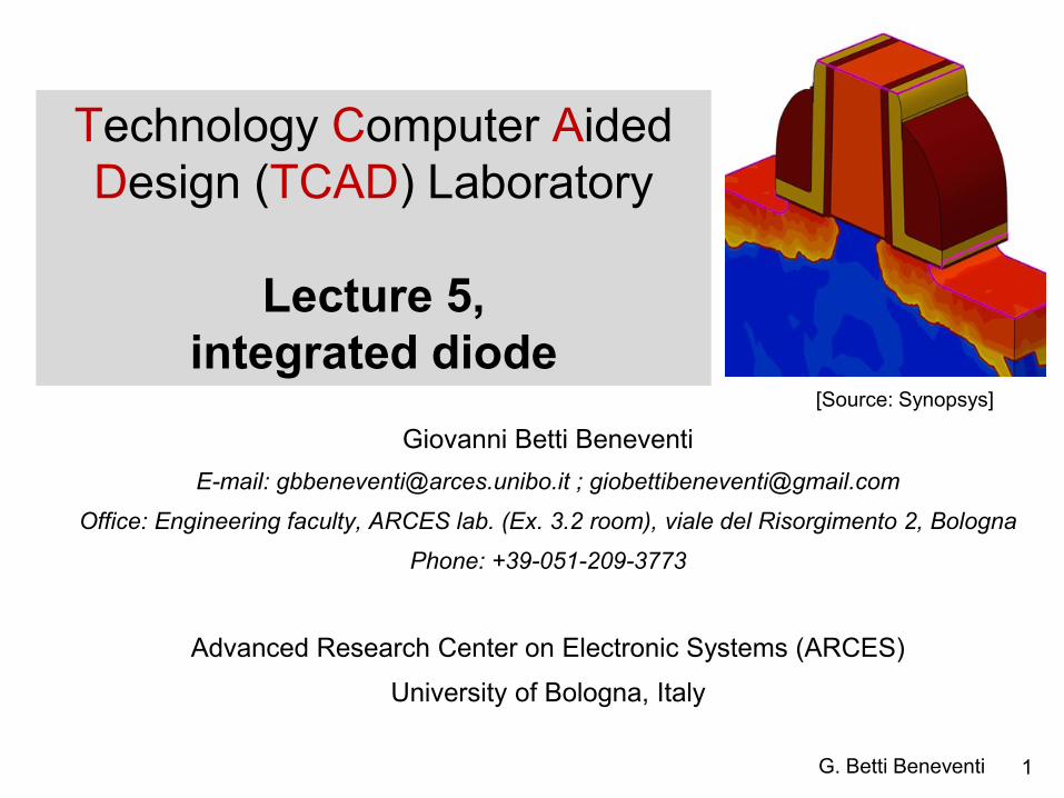
[Source: Synopsys]

2 G. Betti Beneventi
Outline
• Introduction
• Implementation of Input files
– Sentaurus Structure Editor (SDE) command file
– Sentaurus Device (SDevice)
• command file
• parameter file
• Run the simulation
• Post-processing of results

3 G. Betti Beneventi
Introduction
• In this lesson we will implement a more realistic version
of the pn-junction diode.
• The goal is to build a prototype device which could be
similar to actual integrated diodes.
• The more realistic diode has features such as finite
doping abruptness which makes it more suitable to
simulate the reverse bias region including effects such
as the band-to-band tunneling (i.e. Zener effect) or
avalanche generation (i.e. Impact Ionization).
• The reason why these phenomena must be simulated
with finite doping abruptness is that they depend
exponentially on the applied field, and steep fields at the
abrupt junctions could lead to convergence issues.

4 G. Betti Beneventi
Qualitative understanding of band-to-band tunneling (1)
• Band-to-band tunneling is a carrier generation phenomenon.
energy bands under high electric field
in reverse bias region
(assumed linear for simplicity)
EC EV
EG=material bandgap=barrier height
L= length of tunneling path
EG
L
According to quantum mechanics,
if L is short enough and if EG is
small enough there is a not-
negligible probability of an electron
to tunnel from the valence band of
the p-region to the conduction
band of the n-region. In this way,
an electron is injected in the
conduction band and a hole is
freed at the valence band, and can
contribute to current conduction.
This carrier-generation process is
shown to increase exponentially
with the increase of the module of
the reverse electric field. This
phenomenon is also called “Zener
breakdown”.
p-region n-region
5 G. Betti Beneventi
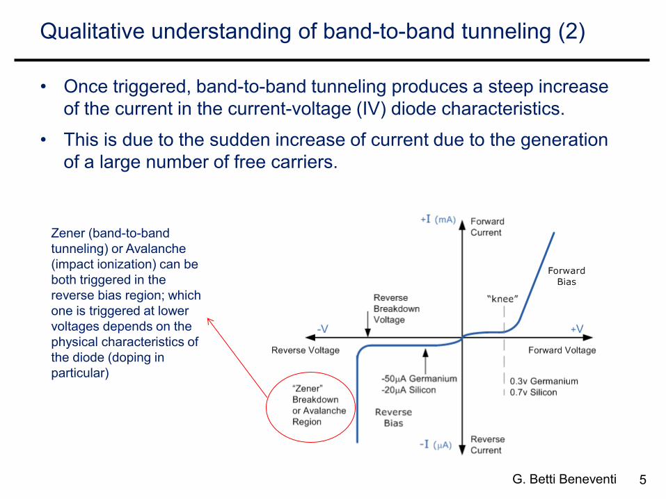
Qualitative understanding of band-to-band tunneling (2)
• Once triggered, band-to-band tunneling produces a steep increase
of the current in the current-voltage (IV) diode characteristics.
• This is due to the sudden increase of current due to the generation
of a large number of free carriers.
Zener (band-to-band
tunneling) or Avalanche
(impact ionization) can be
both triggered in the
reverse bias region; which
one is triggered at lower
voltages depends on the
physical characteristics of
the diode (doping in
particular)

6 G. Betti Beneventi
Band-to-band tunneling & impact ionization
For relatively
high doping
concentrations,
Zener tunneling
occurs at lower
voltages than
Avalanche

7 G. Betti Beneventi
The structure
• We want to create a structure like this one:
p-region contact n-region contact
oxide oxide oxide
p-well
n-well
lightly-doped substrate
junctions
p+ n+
8 G. Betti Beneventi
SWB
OPEN SWB FROM THE LINUX COMMAND LINE
swb &
STARTING (AND SAVING) A NEW SWB PROJECT
Project New New Project
Project Save as Project pn_reale
ADD TOOLS
left click on No tools right click Add Name, scroll for SDE select Batch Ok
left click on SDE right click Add Name scroll for Sdevice Ok
ADD PARAMETERS (WITH THEIR DEFAULT VALUES):
Click above SDE tool image and press Insert Parameter pwell_doping_concentration
default value 5e18
Right click on pwell_doping_concentration Add Parameter
nwell_doping_concentration default value 5e17
Right click in the box just below Sdevice tool image and press Insert Parameter VR
default value -6
Right click on VR Add Parameter VD default value 1
Experiment Add New Experiment pwell_doping_concentration 5e19
nwell_doping_concentration 5e18

9 G. Betti Beneventi
Geometrical definitions / integrated diode
x
y
substrate_length
(0,0)
substrate_
thickness
pwell_
thickness
p_contact_dx
p_contact
_length
nwell_
thickness
n_contact_dx
n_contact_length
p_well_x1 p_well_x2
n_well_x1 n_well_x2
oxide_
thickness
p_well_dx p_well_dx
pwell_doping_concentration nwell_doping_concentration
10 G. Betti Beneventi
SDE command file (1)
Select SDE image tool Right Click Edit input Commands
then write in the text file the following commands:
; clear structure
(sde:clear)
; New-replace-old option (default)
(sdegeo:set-default-boolean "ABA")
; define minimum displacement
(define eps 0.001)
; SEMICONDUCTOR MATERIAL
(define semiconductor_material "Silicon")
; SUBSTRATE PARAMETERS
(define substrate_length 1.400)
(define substrate_thickness 0.800)
; PWELL PARAMETERS
(define pwell_thickness 0.200)
; x coordinate of pwell
(define p_contact_dx 0.400)
(define p_contact_length 0.150)

11 G. Betti Beneventi
SDE command file (2)
; NWELL PARAMETERS
(define nwell_thickness 0.350)
; x coordinate of nwell
(define n_contact_dx 1.000)
(define n_contact_length 0.200)
; extra space at contacts
(define pwell_dx 0.100)
(define pwell_x1 (- p_contact_dx pwell_dx))
(define pwell_x2 (+ pwell_dx (+ p_contact_length p_contact_dx)))
(define nwell_x1 0.150)
(define nwell_x2 (- substrate_length 0.150))
; DOPING PARAMETERS
(define substrate_doping_concentration 1e12)
(define nwell_doping_concentration @nwell_doping_concentration@)
(define pwell_doping_concentration @pwell_doping_concentration@)

12 G. Betti Beneventi
SDE command file (3)
(define nwell_value_at_depth substrate_doping_concentration)
(define nwell_depth 0.050)
(define pwell_value_at_depth substrate_doping_concentration)
(define pwell_depth 0.100)
; OXIDE
(define oxide_material "Oxide")
(define oxide_thickness 0.050)
; MESH PARAMETERS
(define substrate_xmax 0.056)
(define substrate_ymax 0.056)
(define substrate_xmin 0.028)
(define substrate_ymin 0.028)
(define wells_xmax 0.21)
(define wells_ymax 0.21)
(define wells_xmin 0.0056)
(define wells_ymin 0.0056)
parameter
for
Gaussian
smoothing
of doping
(see next)
13 G. Betti Beneventi
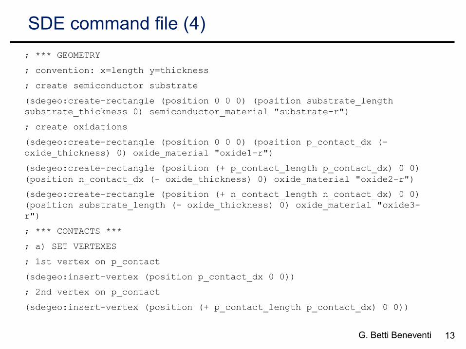
SDE command file (4)
; *** GEOMETRY
; convention: x=length y=thickness
; create semiconductor substrate
(sdegeo:create-rectangle (position 0 0 0) (position substrate_length
substrate_thickness 0) semiconductor_material "substrate-r")
; create oxidations
(sdegeo:create-rectangle (position 0 0 0) (position p_contact_dx (-
oxide_thickness) 0) oxide_material "oxide1-r")
(sdegeo:create-rectangle (position (+ p_contact_length p_contact_dx) 0 0)
(position n_contact_dx (- oxide_thickness) 0) oxide_material "oxide2-r")
(sdegeo:create-rectangle (position (+ n_contact_length n_contact_dx) 0 0)
(position substrate_length (- oxide_thickness) 0) oxide_material "oxide3-
r")
; *** CONTACTS ***
; a) SET VERTEXES
; 1st vertex on p_contact
(sdegeo:insert-vertex (position p_contact_dx 0 0))
; 2nd vertex on p_contact
(sdegeo:insert-vertex (position (+ p_contact_length p_contact_dx) 0 0))

14 G. Betti Beneventi
SDE command file (5)
; 1st vertex on n_contact
(sdegeo:insert-vertex (position n_contact_dx 0 0))
; 2nd vertex on n_contact
(sdegeo:insert-vertex (position (+ n_contact_dx n_contact_length) 0 0))
; b) SET EDGE (DEFINITION AND ACTIVATION)
; p_contact
(sdegeo:define-contact-set "p_contact" 4 (color:rgb 1 0 0) "##")
(sdegeo:set-current-contact-set "p_contact")
(sdegeo:define-2d-contact (find-edge-id (position (+ eps p_contact_dx) 0 0))
"p_contact")
; n_contact
(sdegeo:define-contact-set "n_contact" 4 (color:rgb 1 0 0) "##")
(sdegeo:set-current-contact-set "n_contact")
(sdegeo:define-2d-contact (find-edge-id (position (+ eps n_contact_dx) 0 0))
"n_contact")
15 G. Betti Beneventi
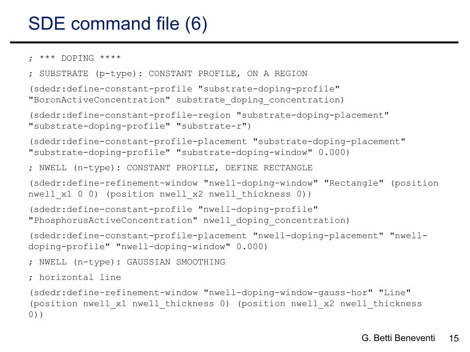
SDE command file (6)
; *** DOPING ****
; SUBSTRATE (p-type): CONSTANT PROFILE, ON A REGION
(sdedr:define-constant-profile "substrate-doping-profile"
"BoronActiveConcentration" substrate_doping_concentration)
(sdedr:define-constant-profile-region "substrate-doping-placement"
"substrate-doping-profile" "substrate-r")
(sdedr:define-constant-profile-placement "substrate-doping-placement"
"substrate-doping-profile" "substrate-doping-window" 0.000)
; NWELL (n-type): CONSTANT PROFILE, DEFINE RECTANGLE
(sdedr:define-refinement-window "nwell-doping-window" "Rectangle" (position
nwell_x1 0 0) (position nwell_x2 nwell_thickness 0))
(sdedr:define-constant-profile "nwell-doping-profile"
"PhosphorusActiveConcentration" nwell_doping_concentration)
(sdedr:define-constant-profile-placement "nwell-doping-placement" "nwell-
doping-profile" "nwell-doping-window" 0.000)
; NWELL (n-type): GAUSSIAN SMOOTHING
; horizontal line
(sdedr:define-refinement-window "nwell-doping-window-gauss-hor" "Line"
(position nwell_x1 nwell_thickness 0) (position nwell_x2 nwell_thickness
0))
16 G. Betti Beneventi
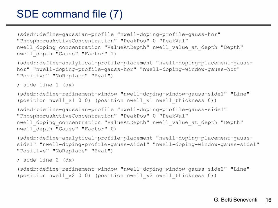
SDE command file (7)
(sdedr:define-gaussian-profile "nwell-doping-profile-gauss-hor"
"PhosphorusActiveConcentration" "PeakPos" 0 "PeakVal"
nwell_doping_concentration "ValueAtDepth" nwell_value_at_depth "Depth"
nwell_depth "Gauss" "Factor" 1)
(sdedr:define-analytical-profile-placement "nwell-doping-placement-gauss-
hor" "nwell-doping-profile-gauss-hor" "nwell-doping-window-gauss-hor"
"Positive" "NoReplace" "Eval")
; side line 1 (sx)
(sdedr:define-refinement-window "nwell-doping-window-gauss-side1" "Line"
(position nwell_x1 0 0) (position nwell_x1 nwell_thickness 0))
(sdedr:define-gaussian-profile "nwell-doping-profile-gauss-side1"
"PhosphorusActiveConcentration" "PeakPos" 0 "PeakVal"
nwell_doping_concentration "ValueAtDepth" nwell_value_at_depth "Depth"
nwell_depth "Gauss" "Factor" 0)
(sdedr:define-analytical-profile-placement "nwell-doping-placement-gauss-
side1" "nwell-doping-profile-gauss-side1" "nwell-doping-window-gauss-side1"
"Positive" "NoReplace" "Eval")
; side line 2 (dx)
(sdedr:define-refinement-window "nwell-doping-window-gauss-side2" "Line"
(position nwell_x2 0 0) (position nwell_x2 nwell_thickness 0))

17 G. Betti Beneventi
SDE command file (8)
(sdedr:define-gaussian-profile "nwell-doping-profile-gauss-side2"
"PhosphorusActiveConcentration" "PeakPos" 0 "PeakVal"
nwell_doping_concentration "ValueAtDepth" nwell_value_at_depth "Depth"
nwell_depth "Gauss" "Factor" 0)
(sdedr:define-analytical-profile-placement "nwell-doping-placement-gauss-
side2" "nwell-doping-profile-gauss-side2" "nwell-doping-window-gauss-side2"
"Negative" "NoReplace" "Eval")
; NWELL OHMIC CONTACT
(sdedr:define-refinement-window "nwell-doping-window-ohmic" "Rectangle"
(position n_contact_dx 0 0) (position (+ n_contact_dx n_contact_length) (*
0.25 nwell_thickness) 0))
(sdedr:define-constant-profile "nwell-doping-profile-ohmic"
"PhosphorusActiveConcentration" 1e20)
(sdedr:define-constant-profile-placement "nwell-doping-placement-ohmic"
"nwell-doping-profile-ohmic" "nwell-doping-window-ohmic" 0.000)
; PWELL (p-type): CONSTANT PROFILE
(sdedr:define-refinement-window "pwell-doping-window" "Rectangle" (position
pwell_x1 0 0) (position pwell_x2 pwell_thickness 0))
(sdedr:define-constant-profile "pwell-doping-profile"
"BoronActiveConcentration" pwell_doping_concentration)
(sdedr:define-constant-profile-placement "pwell-doping-placement" "pwell-
doping-profile" "pwell-doping-window" 0.000)
18 G. Betti Beneventi
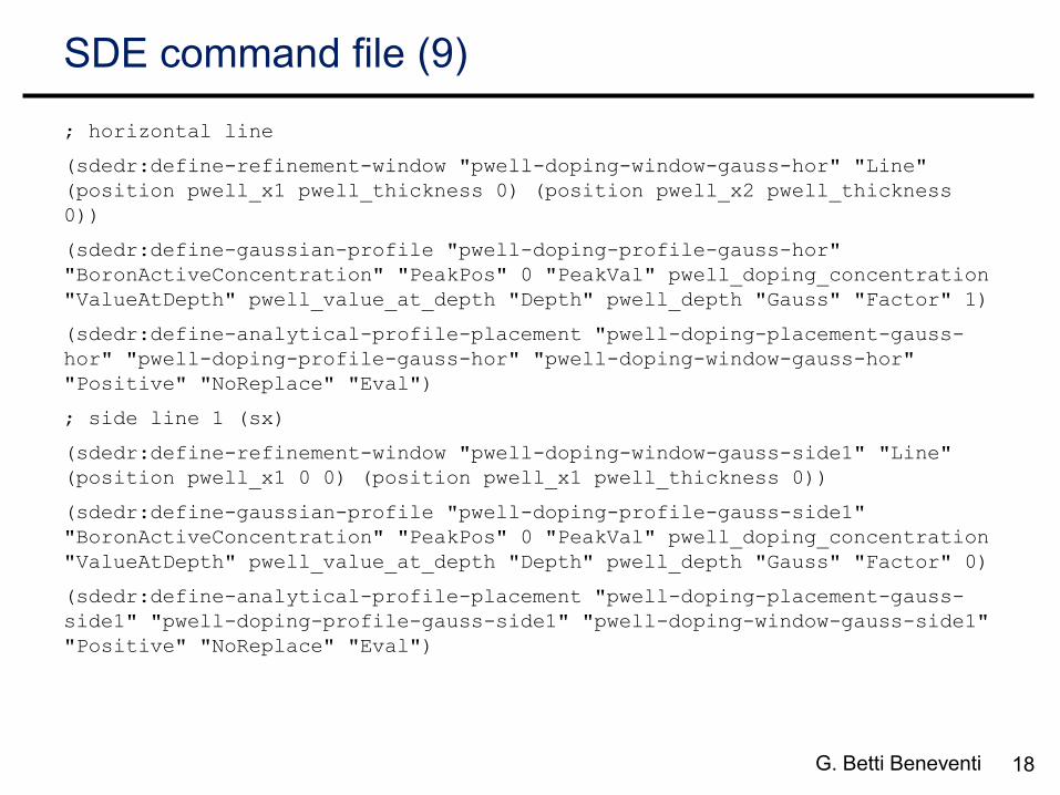
SDE command file (9)
; horizontal line
(sdedr:define-refinement-window "pwell-doping-window-gauss-hor" "Line"
(position pwell_x1 pwell_thickness 0) (position pwell_x2 pwell_thickness
0))
(sdedr:define-gaussian-profile "pwell-doping-profile-gauss-hor"
"BoronActiveConcentration" "PeakPos" 0 "PeakVal" pwell_doping_concentration
"ValueAtDepth" pwell_value_at_depth "Depth" pwell_depth "Gauss" "Factor" 1)
(sdedr:define-analytical-profile-placement "pwell-doping-placement-gauss-
hor" "pwell-doping-profile-gauss-hor" "pwell-doping-window-gauss-hor"
"Positive" "NoReplace" "Eval")
; side line 1 (sx)
(sdedr:define-refinement-window "pwell-doping-window-gauss-side1" "Line"
(position pwell_x1 0 0) (position pwell_x1 pwell_thickness 0))
(sdedr:define-gaussian-profile "pwell-doping-profile-gauss-side1"
"BoronActiveConcentration" "PeakPos" 0 "PeakVal" pwell_doping_concentration
"ValueAtDepth" pwell_value_at_depth "Depth" pwell_depth "Gauss" "Factor" 0)
(sdedr:define-analytical-profile-placement "pwell-doping-placement-gauss-
side1" "pwell-doping-profile-gauss-side1" "pwell-doping-window-gauss-side1"
"Positive" "NoReplace" "Eval")
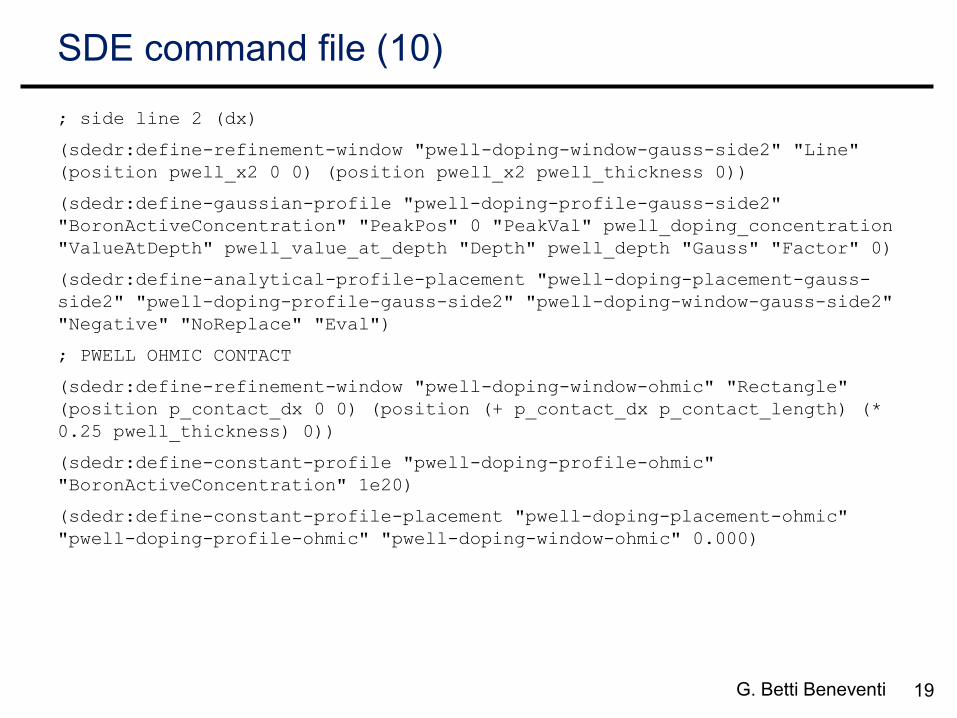
19 G. Betti Beneventi
SDE command file (10)
; side line 2 (dx)
(sdedr:define-refinement-window "pwell-doping-window-gauss-side2" "Line"
(position pwell_x2 0 0) (position pwell_x2 pwell_thickness 0))
(sdedr:define-gaussian-profile "pwell-doping-profile-gauss-side2"
"BoronActiveConcentration" "PeakPos" 0 "PeakVal" pwell_doping_concentration
"ValueAtDepth" pwell_value_at_depth "Depth" pwell_depth "Gauss" "Factor" 0)
(sdedr:define-analytical-profile-placement "pwell-doping-placement-gauss-
side2" "pwell-doping-profile-gauss-side2" "pwell-doping-window-gauss-side2"
"Negative" "NoReplace" "Eval")
; PWELL OHMIC CONTACT
(sdedr:define-refinement-window "pwell-doping-window-ohmic" "Rectangle"
(position p_contact_dx 0 0) (position (+ p_contact_dx p_contact_length) (*
0.25 pwell_thickness) 0))
(sdedr:define-constant-profile "pwell-doping-profile-ohmic"
"BoronActiveConcentration" 1e20)
(sdedr:define-constant-profile-placement "pwell-doping-placement-ohmic"
"pwell-doping-profile-ohmic" "pwell-doping-window-ohmic" 0.000)
20 G. Betti Beneventi
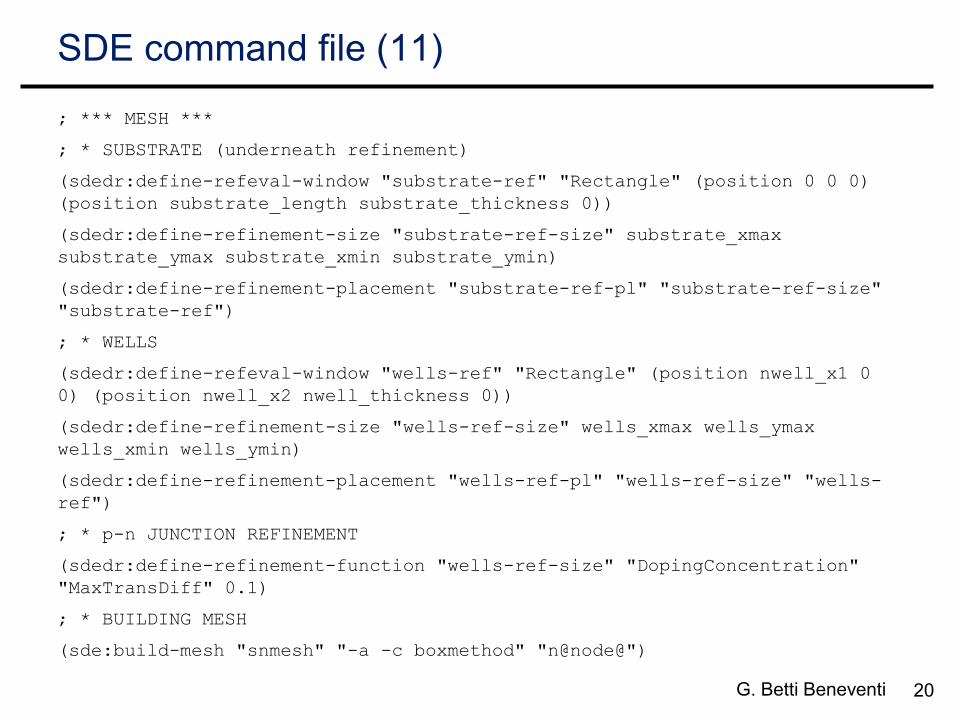
SDE command file (11)
; *** MESH ***
; * SUBSTRATE (underneath refinement)
(sdedr:define-refeval-window "substrate-ref" "Rectangle" (position 0 0 0)
(position substrate_length substrate_thickness 0))
(sdedr:define-refinement-size "substrate-ref-size" substrate_xmax
substrate_ymax substrate_xmin substrate_ymin)
(sdedr:define-refinement-placement "substrate-ref-pl" "substrate-ref-size"
"substrate-ref")
; * WELLS
(sdedr:define-refeval-window "wells-ref" "Rectangle" (position nwell_x1 0
0) (position nwell_x2 nwell_thickness 0))
(sdedr:define-refinement-size "wells-ref-size" wells_xmax wells_ymax
wells_xmin wells_ymin)
(sdedr:define-refinement-placement "wells-ref-pl" "wells-ref-size" "wells-
ref")
; * p-n JUNCTION REFINEMENT
(sdedr:define-refinement-function "wells-ref-size" "DopingConcentration"
"MaxTransDiff" 0.1)
; * BUILDING MESH
(sde:build-mesh "snmesh" "-a -c boxmethod" "n@node@")

21 G. Betti Beneventi
SDE command file (12)
• Save Quit
DONE SDE PART.
point 1
point 2 baseline
"Negative"
Gaussian
shoulder
N.B how to handle "Positive" and "Negative" in the Gaussian doping profile:
"Positive"
Gaussian
shoulder
22 G. Betti Beneventi
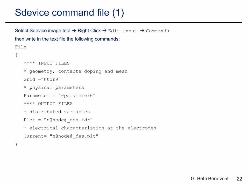
Sdevice command file (1)
Select Sdevice image tool Right Click Edit input Commands
then write in the text file the following commands:
File
{
**** INPUT FILES
* geometry, contacts doping and mesh
Grid ="@tdr@"
* physical parameters
Parameter = "@parameter@"
**** OUTPUT FILES
* distributed variables
Plot = "n@node@_des.tdr"
* electrical characteristics at the electrodes
Current= "n@node@_des.plt"
}

23 G. Betti Beneventi
Sdevice command file (2)
Electrode
{
* defines which contacts have to be treated as electrodes; initial bias
& boundary conditions
* obviously, electrode names must match the contact names of the dvs.cmd
file
{ name="p_contact" voltage=0.0 }
{ name="n_contact" voltage=0.0 }
Physics
{
Mobility (
DopingDependence
)
Recombination (
SRH (DopingDependence)
SRH (TemperatureDependence)
advanced SRH models

24 G. Betti Beneventi
Sdevice command file (3)
Band2BandTunneling
)
}
Plot
{
* On mesh variables to be saved in the .tdr output file
*- Doping Profiles
Doping DonorConcentration AcceptorConcentration
*- Charge, field, potential and potential energy
SpaceCharge
ElectricField/Vector Potential
BandGap EffectiveBandGap BandGapNarrowing ElectronAffinity
ConductionBandEnergy ValenceBandEnergy
*- Carrier Densities:
EffectiveIntrinsicDensity IntrinsicDensity
eDensity hDensity
eQuasiFermiEnergy hQuasiFermiEnergy
Band-to-band tunneling default model

25 G. Betti Beneventi
Sdevice command file (4)
*- Currents and current components:
eGradQuasiFermi/Vector hGradQuasiFermi/Vector
eMobility hMobility eVelocity hVelocity
Current/Vector eCurrent/Vector hCurrent/Vector
eDriftVelocity/Vector hDriftVelocity/Vector
*- SRH & interfacial traps
SRHrecombination
tSRHrecombination
*- Band2Band Tunneling
eBand2BandGeneration hBand2BandGeneration Band2BandGeneration
eAvalanche hAvalanche
}
Math
{
* use previous two solutions (if any) to extrapolate next
Extrapolate

26 G. Betti Beneventi
Sdevice command file (5)
* use full derivatives in Newton method
Derivatives
* control on relative errors
RelErrControl
* relative error= 10^(-Digits)
Digits=7
* absolute error
Error(electron)=1e8
Error(hole)=1e8
* numerical parameter for space-charge regions
eDrForceRefDens=1e10
hDrForceRefDens=1e10
* maximum number of iteration at each step
Iterations=20
Method=ParDiSo
7 rather than 5 to
increase convergence robustness

27 G. Betti Beneventi
Sdevice command file (6)
* display simulation time in 'human' units
Wallclock
* display max.error information
CNormPrint
* to avoid convergence problem when simulating defect-assisted tunneling
NoSRHperPotential
}
Solve
{
coupled {poisson}
coupled {poisson electron hole}
** TURN-ON
* decreasing p_contact to goal
quasistationary (InitialStep = 1e-3 MaxStep = 1e-3 MinStep=1e-6
Goal {name= "p_contact" voltage = @VR@}
plot { range=(0, 1) intervals=1 }
)
{coupled {poisson electron hole} }
compute also current continuity +
transport equations at equilibrium
increase convergence robustness
(provide better first guess to n and p
for non zero current)
28 G. Betti Beneventi
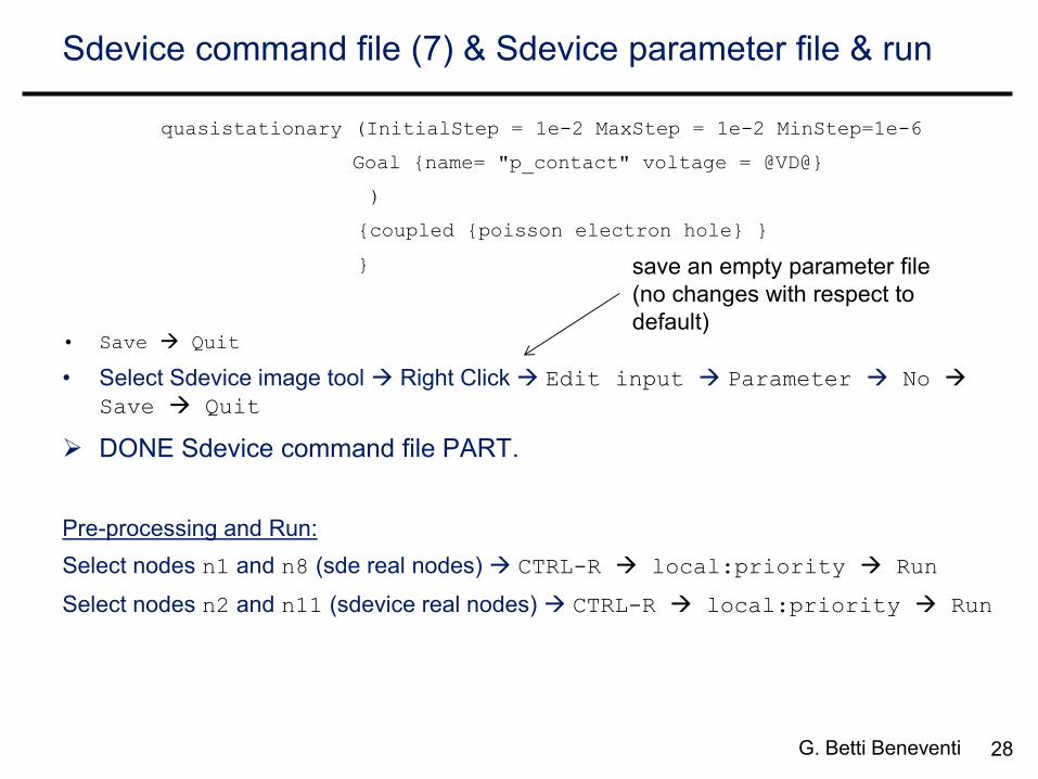
Sdevice command file (7) & Sdevice parameter file & run
quasistationary (InitialStep = 1e-2 MaxStep = 1e-2 MinStep=1e-6
Goal {name= "p_contact" voltage = @VD@}
)
{coupled {poisson electron hole} }
}
• Save Quit
• Select Sdevice image tool Right Click Edit input Parameter No
Save Quit
DONE Sdevice command file PART.
Pre-processing and Run:
Select nodes n1 and n8 (sde real nodes) CTRL-R local:priority Run
Select nodes n2 and n11 (sdevice real nodes) CTRL-R local:priority Run
save an empty parameter file
(no changes with respect to
default)
29 G. Betti Beneventi
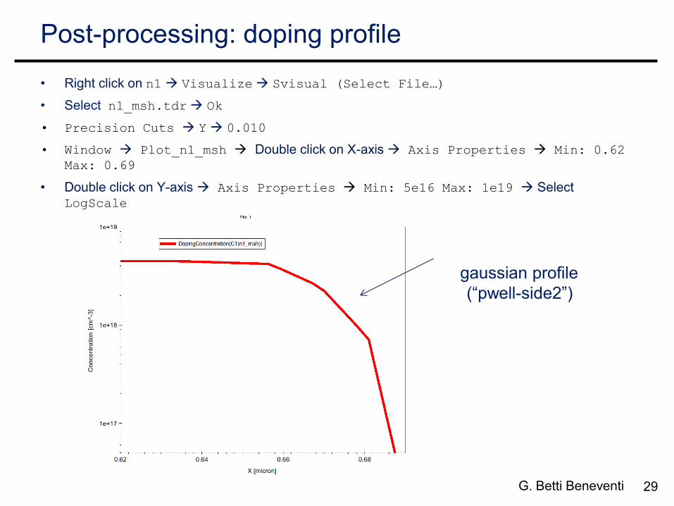
Post-processing: doping profile
• Right click on n1 Visualize Svisual (Select File…)
• Select n1_msh.tdr Ok
• Precision Cuts Y 0.010
• Window Plot_n1_msh Double click on X-axis Axis Properties Min: 0.62
Max: 0.69
• Double click on Y-axis Axis Properties Min: 5e16 Max: 1e19 Select LogScale
gaussian profile
(“pwell-side2”)

30 G. Betti Beneventi
Post-processing: IV curve
• Right click on n2 and n11 Visualize Inspect (All Files)
• Select n2 and n11 on the Datasets part p_contact OuterVoltage To X-Axis
TotalCurrent To Left-Y-Axis
• Select logY on the upper toolbar
logY
onsets of breakdown decreases for increasing doping

31 G. Betti Beneventi
Post-processing: reverse bias bands
• Right click on n11 Visualize Svisual (Select File…)
• Select n11_000001_des Ok
• Precision Cuts Y 0.05 Plot Band Diagram
• Double click on the x-axis of the band diagram Axis Properties Min. 0.60 Max.
0.75
• Window Plot n11_000001_des
EV=EC
available
window for
direct band-
to-band
tunneling

32 G. Betti Beneventi
Post-processing: band-to-band generation rates
• Window Plot n11_000001_des Window Plot1
• Scalars Band2BandGeneration zoom at the junction
pwell
33 G. Betti Beneventi
Bibliography
• S.Sze, Physics of Semiconductors Devices, 2nd edition, 1981.
• Sentaurus Synopys User’s guides