technical document for: umodem ( usb modem )
TRANSCRIPT
Research & Development
Technical Document for:
uModem ( USB Modem )
Revision Issue Date Engineer/Comments 1.0 November 22, 2002 YLYang/Pre-release
Copyright by 3JTech. Co., Ltd. All rights reserved.
Page 1 of 1Revision 1.0 2003/6 From 3JTech

Research & Development
3JTech 56K USB modem solution _ uModem Single chip ZD1051 integrates DSP, controller and USB interface Power management chip ZD1056 supports USB bus-powered design Features ● Data mode - ITU-T V.90 / V.34 (33.6K) / V.32b / V.32 / V.22b / V.22 / V.23 / V.21
- Bell 212A/ Bell 103 - Error correction: ITU-T V.42 and MNP3,4 - Data compression: ITU-T V.42b and MNP5 - Industry standard AT command sets - Caller ID
● FAX mode - ITU-T V.17/ V.29/ V27ter up to 14.4K bps - TIA class1/ 2/ 2.0 fax command sets ● USB features
- USB specification 1.1 compliant - power management: bus-powered, suspend mode supported - full speed 12 Mbps
● System compatibility - Microsoft Windows 98 and Windows 2000 - Macintosh MacOS.9.0
● Voice features - Voice compression : 4-bit ADPCM
- TIA IS-101 voice command set - TAM function ● World wide homologation - FCC Part 68/ CTR21 versions
- Programmable PTT parameters ● Electrical characteristics - ZD1051 Package: 128-pin TQFP, 3.3V/1.8V dual power mode, 3.3V for I/O pad and 1.8V for core operation
General Description The highly-integrated ZD1051 56K USB modem chip uses only one DSP core, embedded in the ZD1051, to handle both the signal and protocol processing. No controller is needed for modem protocol handling. This kind of integration not only shrinks the modem chipset into a single chip but also improves hardware reliability and reduces the power consumption. An extremely small 128-pin TQFP package, 16x16 mm square, is easily fitted to any critical PCB design. The power dissipation of ZD1051 is less than 220 mW, ZD1051 is suitable for power-sensitive portable applications. This solution also adopts the latest silicon DAA technology with programmable characteristics; this makes it possible to meet the world wide PTT certifications using a single hardware. ZyDAS USB modem solution is the best choice for designing a 56K USB external modem. Applications ●USB external modem for Internet access ●USB external modem for Internet games (PS2) Solutions ● ZyDAS ZD1051 USB 56K modem data pump ● ZyDAS ZD10591 USB 56K modem ROM code (optional) ● Silicon Lab Si3034/Si3035 silicon DAA
EEPROM2K bits
Telephone Line
USB Bus
SRAM64Kx16
ROM256Kx16
(FEPROM/MROM)
Silicon DAASi3034 /Si3035
ZyDAS 56KModem Data Pump
ZD1051128-Pin TQFP
Figure 1. 3JTech USB modem simplified diagram
Page 2 of 2Revision 1.0 2003/6 From 3JTech
Research & Development
FUNCTION DESCRIPTIONS ZyDAS USB modem uses a hardware-based DSP core to handle both the modem signal processing and modem protocol processing in a single chip. and an embedded USB logic to process host USB traffic in a single chip. This chip supports to run a data/fax modem implementation and voice compression algorithm processing for Telephone Answering Machine (TAM) application. The major functions of ZyDAS USB modem are described below. USB functions ● CDC 1.1 compliant for different platforms: CDC, communication device class for USB devices, is an interface between USB hosts and USB devices. The purpose of CDC is to support all kinds of communication services on the USB. ZyDAS USB USB modem meets the CDC version 1.1 specifications and can talk to hosts supporting CDC driver. No special USB drivers are needed in such kind of hosts. Currently, the Win 98 SE, Win 98 ME, Win 2000 and MacOS.9.0 are all CDC ready. ZyDAS also provides the USB CDC drivers for the first edition of Win98 system. ● Power management - suspend and resume: USB hosts can supply power to USB devices directly connected to the bus. USB hosts may also have the power management capability to suspend or resume the USB bus-powered devices in any power-sensitive portable applications such as NB or PDA. ZyDAS 56K USB modem solution includes a power management chip - ZD1056, which can allow the USB host to order the modem to enter into suspend mode to save power consumption. ZyDAS 56K USB modem will resume from suspend state when ordered by the host. In addition to this, the modem can also resume and trigger a remote-wake-up signal to the host when there is an incoming call. Data/Fax mode ● Data and fax mode auto discrimination: Data or fax incoming calls can be automatically recognized as a data or fax connection without the user intervention. ● Multi-auto mode V.90 modem: In ITU-T V.90 data mode, ZyDAS USB modem can receive data at speeds up to 56K bps while connecting to a digitally connected central modem. Due to the PSTN network's digitization, only the client modem to central office local loop is not digital. This V.90 data pump is very suitable for remote access applications such as Internet access, remote on-line service and corporate data base access.
ZyDAS 56K USB modem conforms to ITU-T V.34 standard, operates in two-wire full duplex asynchronous mode at line speeds up to 33.6Kbps. Based on ZyDAS's own DSP algorithm, this modem can maintain high quality connections at high speeds especially under adverse line conditions. It will automatically fall back to lower speeds when communicating with slower modems or when line condition degrades. ITU-T T.30 fax protocol describes the G3 fax handshake signals and procedures. ZyDAS USB modem takes full control of this protocol, initiates and terminates fax calls, manages the communication session and transports the image data, provides the highest fax speed of up to 14.4 Kbps using the fax transmission standard V.17. This modem supports TIA Class 1, Class 2 and Class 2.0 command sets. Voice mode Voice mode of ZyDAS USB modem stands for the ability to digitize incoming voice messages such that the computer can store and forward them. It also playbacks the recorded digitized voice on line for a message announcement. This modem uses 9.6 KHz/ 8KHz sampling rates and chooses a high voice quality 4-bit ADPCM algorithm to reduce the speech data rate. IS-101 voice command set and DTMF detection are supported. World wide homologation ZyDAS USB modem uses the programmable silicon DAA Si3034/ Si3035 as the analog front end. The Si3034 DAA which is the international version meets most of the world wide PTT specifications and Si3035, the FCC version, meets the FCC PTT specification. ZyDAS provides a tool to change the parameters used for call progress monitoring, dialing, and ring detection. Modem designer can use this tool to change the PTT parameters to precede the new PTT type approvals. The parameters for CTR21 and FCC Part 68 compliance are provided. Reference design A reference USB bus modem design with data/fax/TAM function is ready for evaluation. This design can pass the pretest of EMC, safety and PTT certifications. The schematic, BOM, board layout of this design are all available. Designer can use this as a reference to shorten the design cycle and finish the prototype rapidly.
Page 3 of 3Revision 1.0 2003/6 From 3JTech

Research & Development
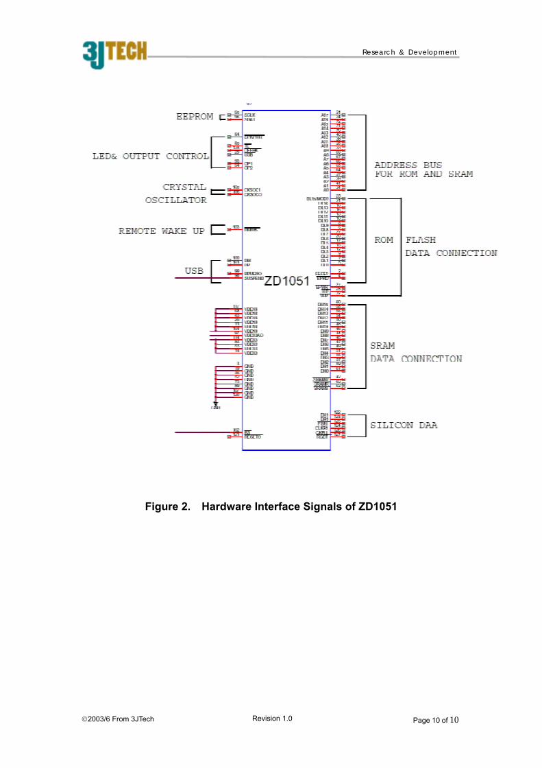
HARDWARE DESCRIPTIONS ZyDAS 56K USB modem solution includes the modem data pump ZD1051 and Silicon Lab's Si3034/ Si3035 silicon DAA. ZyDAS also provides an optional ROM code ZD10591 to replace the FEPROM used in this modem. The hardware function of ZD1051 is described herein. Please refer to the hardware interface signals of ZD1051 in Figure 2 for the usage of ZD1051. ZD1051 Modem Data Pump The ZD1051 modem data pump consists of a high performance / low power consumption DSP core, a high speed data bus for data memory, a low speed data bus for program memory, a USB transfer, a serial interface for silicon DAA and a serial EEPROM interface for modem profiles. ZD1051 gets the transmit data from the USB transfer. This data bit stream is converted to an voice band signal by the ZD1051's DSP core and sent to the telephone line via the silicon DAA to the remote modem. The analog waveform on the telephone line coming from the remote modem is digitized by the silicon DAA. This digitized signal is demodulated as received data bit stream by the DSP core and then transferred to host through the USB transfer. The access time of the SRAM connected to the high speed data bus of ZD1051 must be at least 12 nsec. The access time of FEPROM or ROM connected to the low speed data bus of ZD1051 should be faster than 120 nsec. The functions of ZD1051 from the view point of hardware signals are described as follows. Power signals (19 pins) The ZD1051 uses two power supply voltages, 3.3V and 1.8V. 1.8V is used for the operation of DSP core and logic circuits. 3.3V is used solely for the I/O pads interfacing to 3.3V peripheral chips. ● VDD33: The 3.3V power source. ● VDD18: The 1.8V power source. Reset signals (2 pins) ● RS#: power on reset input pin. A RC network
can be directly connected to the RS# input pin to generate the desired reset signal when turning on the system power. (3.3V input, active low)
● RESETO#: This reset output is used to reset peripheral circuits, such as FEPROM and
Silicon Lab's DAA circuit. It is active low when pin RS# is active. (3.3V output, active low)
Clock signals (2 pins) The clock input frequency is 12 MHz, either an external clock source or a parallel-mode crystal circuit can be used as the clock input of ZD1051. ● CKSOCI: Crystal oscillator input or the input
from an external clock source. (1.8V input) ● CKSOCO: Crystal oscillator output. Leave this
pin open when an external clock source is connected to CKSOCI. (1.8V output)
USB interfaces (4 pins) This interface complies with the USB specification revision 1.1, supporting 12M bps full speed and power management requirement. ● DP: USB data signal Data Plus (D+) connects to USB. (Bi-directional I/O) ● DM: USB data signal Data Minus (D-) connects to USB. (Bi-directional I/O) ● SUSPEND: This USB suspend output signal is used to shut off the power of modem when USB is in suspending state. Connect to the SHDN input of ZD1056 to save the power. (3.3V output, active high) ● RPUENO: Use for USB connects or disconnect control. When reset signal RS# input is low, this pin is tractate. (3.3V output) Remote wakeup (1 pin) When the bus-powered USB modem is in the suspend state, all the modem circuits, including ZD1051 and silicon DAA, are powered off except the always powered circuit in ZD1051. A ring detection circuit not depending on the switched power acts as the wakeup signal. This wakeup signal will be passed to the USB block of ZD151 which will then initiate the resume operation. The first action of the resume operation is turning off the SUSPEND output and power will be resupplied to the modem circuit. Two ring detection circuits are needed for a USB bus-powered modem. One must work in the suspend mode and act to wake up the USB function. The other ring detection circuit is built-in in the Si3034/Si3035 silicon DAA. It is the normal ring detection circuit and can not work in the suspend mode because power to the Si3034/Si3035 is shut off. ● RMWK#: Remote wakeup input for wakeup from USB suspend state. Connect to the output of an up to ring detector. If the remote wakeup function is not used, leave this pin open (3.3V input, active low)
Page 4 of 4Revision 1.0 2003/6 From 3JTech
Research & Development
NVRAM EEPROM interface (2 pins) 24C02 type 2K bits serial EEPROM is used to store the modem configuration profiles and telephone numbers. One user defined profile and four telephone numbers can be saved in this EEPROM. Two pins are used to interface with 24C02. One pin is used as serial clock output pin; the other pin has an open drain output with pullup resistor used for both serial data in and out. ● SCLK: Serial clock output for 24C02 type
EEPROM. Connect this pin to the EEPROM's SCL pin. (3.3V output)
● SDAT: Bi-directional data signal for 24C02 type EEPROM. Connect this pin to the EEPROM's SDA pin. (3.3V bi-directional I/O)
Program memory interface The program memory needed for ZyDAS USB modem solution is 4M bits. This memory device can be flash EPROM, EPROM or ROM. It is connected to the 16-bit low speed data bus of ZD1051. The access time is 120 nsec. The program memory interface is: ● A[17:0]: Address bus lines. (3.3V output) ● DL[15:0]: The low speed data bus lines. (3.3V
I/O) ● FECE1#: Chip select (enable) signal output for
connection to external FEPROM/ EPROM/ ROM device's CE# pin. (3.3V output, active low)
● EPRD#: Read strobe (output enable) signal output for external FEPROM/ EPROM/ ROM device. Connect it to the external device's OE#. (3.3V output, active low)
Note: ZyDAS modem code supports on-chip FEPROM programming capability. Most of the bottom-boot FEPROM can be used. Currently Intel 28F400/28F800 and AMD 29F400/29F800 are supported. The additional FEPROM interface for 28F400 is: ● EPWR#: Write strobe signal output for
FEPROM device. Connect it to the FEPROM's WE# pin (3.3V output, active low)
● WP#: Write protect signal for FEPROM device. Connect it to the FEPROM's WP# pin. (3.3V output, active low)
● VPP#: Control the supply power for FEPROM program and erase operation. (3.3V output, active low)
The additional FEPROM interface signal needed for programming and erasing AMD 29F400 is only EPWR#.
Data memory interface The data memory interface is used to interface high speed SRAM. ZyDAS USB modem needs a 1M bits 12 nsec SRAM. This SRAM is connected to the high speed data bus of ZD1051. ● A [17:0]: Address bus lines are the same as
program memory address bus A[17:0]. (3.3V output)
● DH[15:0]: The high speed data bus lines (3.3V I/O)
● SRAMS#: SRAM chip select signal output for external high speed SRAM. Connect to an SRAM's CE# pin. (3.3V output, active low)
● SRAMR#: SRAM output enable signal output for external high speed SRAM. Connect to an SRAM's OE# pin. (3.3V output, active low)
● SRAMW#: SRAM write strobe signal output for external high speed SRAM. Connect to an SRAM's WE# pin. (3.3V output, active low)
Serial device interface (6 pins) This serial interface is used to connect external silicon DAA. Silicon Lab Si3034/Si3035 silicon DAA can be connected to the ZD1051 through this serial interface. ● CKPLL: 6.144 MHz master clock output to the
front end chip. To be connected to the Si3034/ Si3035's MCLK pin. (3.3V output)
● CLKR1: DSP serial data clock input pin. Connects to the SCLK pin of Si3034/ Si3035. (3.3V input)
● FSR1#: Frame sync input pin for DSP serial port. Connects to the FSYNC# pin of Si3034/ Si3035. (3.3V input)
● DR1: Data input pin for DSP serial port. Connects to the SDO pin of Si3034/ Si3035. (3.3V input)
● DX1: Data output pin for DSP serial port. Connects to the SDI pin of Si3034/ Si3035. (3.3V output)
● RGDT#: The ring detection input, it is connected to pin RGDT# of Silicon DAA Si3034/ Si3035. (3.3V input, active low)
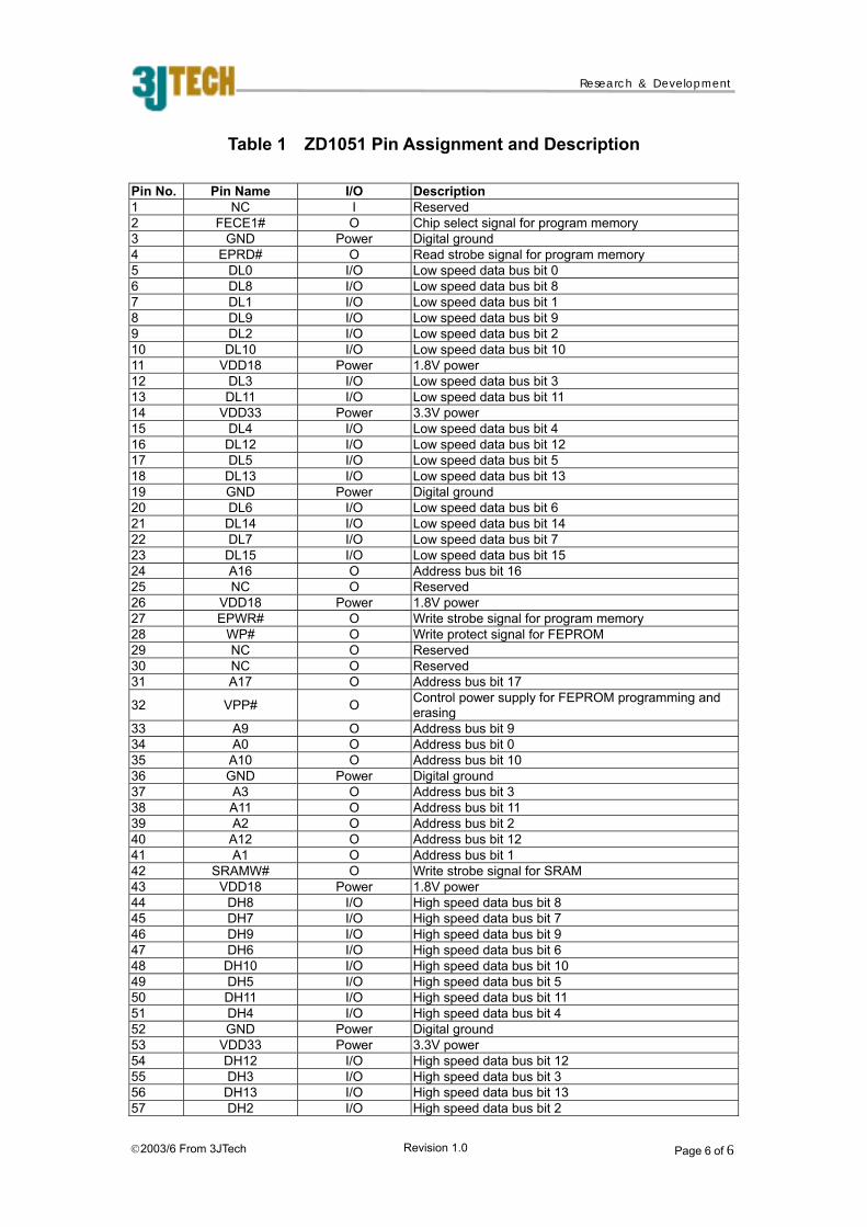
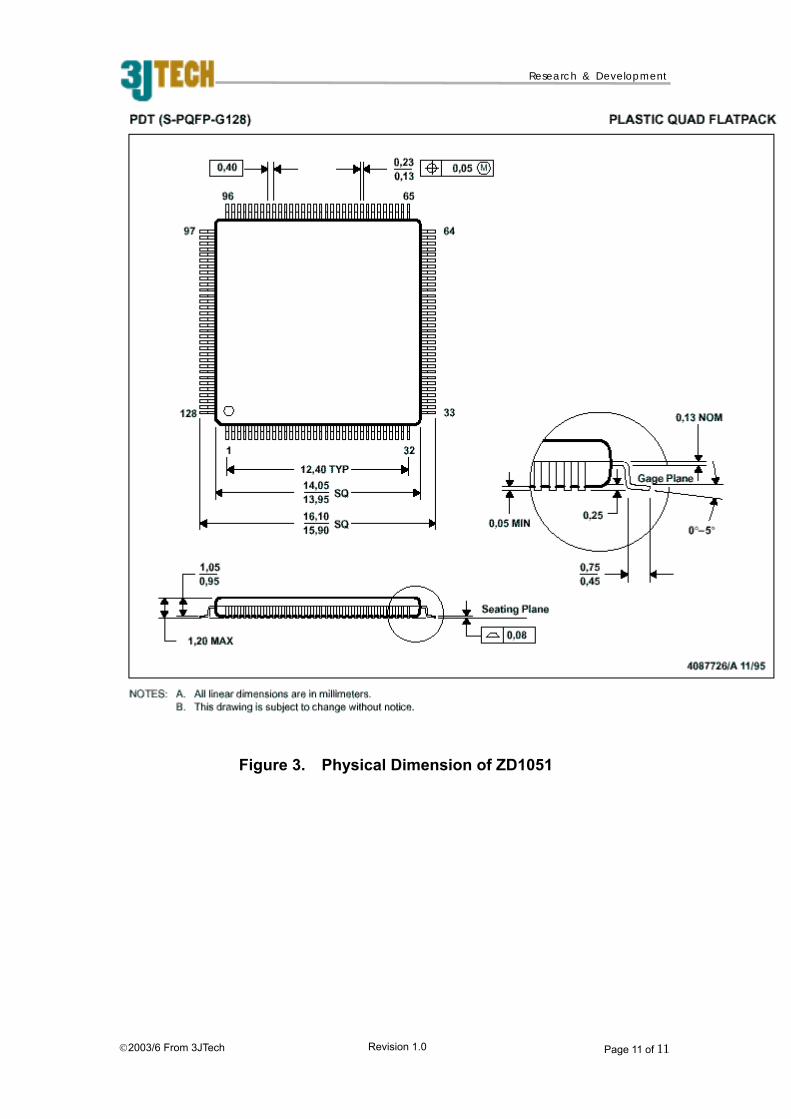
Package and pin assignments ZD1051 is in a 128-pin TQFP package. Please refer to Figure 3 for the physical dimension description. The pin assignments are shown in Table 1. Electrical characteristic Please refer to Table 2.
Page 5 of 5Revision 1.0 2003/6 From 3JTech
Research & Development
Table 1 ZD1051 Pin Assignment and Description
Pin No. Pin Name I/O Description 1 NC I Reserved 2 FECE1# O Chip select signal for program memory 3 GND Power Digital ground 4 EPRD# O Read strobe signal for program memory 5 DL0 I/O Low speed data bus bit 0 6 DL8 I/O Low speed data bus bit 8 7 DL1 I/O Low speed data bus bit 1 8 DL9 I/O Low speed data bus bit 9 9 DL2 I/O Low speed data bus bit 2 10 DL10 I/O Low speed data bus bit 10 11 VDD18 Power 1.8V power 12 DL3 I/O Low speed data bus bit 3 13 DL11 I/O Low speed data bus bit 11 14 VDD33 Power 3.3V power 15 DL4 I/O Low speed data bus bit 4 16 DL12 I/O Low speed data bus bit 12 17 DL5 I/O Low speed data bus bit 5 18 DL13 I/O Low speed data bus bit 13 19 GND Power Digital ground 20 DL6 I/O Low speed data bus bit 6 21 DL14 I/O Low speed data bus bit 14 22 DL7 I/O Low speed data bus bit 7 23 DL15 I/O Low speed data bus bit 15 24 A16 O Address bus bit 16 25 NC O Reserved 26 VDD18 Power 1.8V power 27 EPWR# O Write strobe signal for program memory 28 WP# O Write protect signal for FEPROM 29 NC O Reserved 30 NC O Reserved 31 A17 O Address bus bit 17
32 VPP# O Control power supply for FEPROM programming and erasing
33 A9 O Address bus bit 9 34 A0 O Address bus bit 0 35 A10 O Address bus bit 10 36 GND Power Digital ground 37 A3 O Address bus bit 3 38 A11 O Address bus bit 11 39 A2 O Address bus bit 2 40 A12 O Address bus bit 12 41 A1 O Address bus bit 1 42 SRAMW# O Write strobe signal for SRAM 43 VDD18 Power 1.8V power 44 DH8 I/O High speed data bus bit 8 45 DH7 I/O High speed data bus bit 7 46 DH9 I/O High speed data bus bit 9 47 DH6 I/O High speed data bus bit 6 48 DH10 I/O High speed data bus bit 10 49 DH5 I/O High speed data bus bit 5 50 DH11 I/O High speed data bus bit 11 51 DH4 I/O High speed data bus bit 4 52 GND Power Digital ground 53 VDD33 Power 3.3V power 54 DH12 I/O High speed data bus bit 12 55 DH3 I/O High speed data bus bit 3 56 DH13 I/O High speed data bus bit 13 57 DH2 I/O High speed data bus bit 2
Page 6 of 6Revision 1.0 2003/6 From 3JTech

Research & Development
58 DH14 I/O High speed data bus bit 14 59 DH1 I/O High speed data bus bit 1 60 DH15 I/O High speed data bus bit 15 61 DH0 I/O High speed data bus bit 0 62 SRAMS# O Chip select signal for SRAM 63 SRAMR# O Output enable signal for SRAM 64 A4 O Address bus bit 4 65 A5 O Address bus bit 5 66 A6 O Address bus bit 6 67 A7 O Address bus bit 7 68 VDD18 Power 1.8V power 69 A8 O Address bus bit 8 70 A13 O Address bus bit 13 71 A14 O Address bus bit 14 72 A15 O Address bus bit 15 73 NC O Reserved 74 NC I Reserved 75 GND Power Digital ground 76 NC O Reserved 77 NC I Reserved 78 NC I Reserved 79 NC O Reserved 80 NC O Reserved 81 NC O Reserved 82 NC I Reserved 83 VDD33 Power 3.3V power 84 NC O Reserved
85 TE# O Control the optional relay to switch off the attached telephone set
86 NC O Reserved
87 HS# O Indicate modem in a V.90 connection or, when flashing, in handshaking procedure
88 NC I Reserved 89 GND Power Digital ground
90 AA# O Indicate modem in auto answer mode or, when flashing, detects an incoming ring signal
91 NC I Reserved 92 NC I Reserved 93 OP1 O General purpose output pin 94 OP2 O General purpose output pin 95 SCLK O Serial clock output for EEPROM 96 SDAT IO Serial bi-directional data signal for EEPROM 97 VDD33 Power 3.3V power 98 SUSPEND O USB suspend signal output 99 RPUENO O USB connect or disconnect control 100 DM I/O USB data signal DM(D-) 101 DP I/O USB data signal DP(D+) 102 RS# I Reset signal input (active low) 103 RMWK# I Reserved 104 VDD18 Power 1.8V power 105 CKSOCI I, 1.8V Crystal oscillator input 106 CKSOCO O, 1.8V Crystal oscillator output 107 GND Power Digital ground 108 NC I Reserved 109 NC I Reserved 110 NC O Reserved 111 NC I Reserved 112 NC I Reserved 113 NC I/O Reserved 114 VDD33 Power 3.3V power 115 NC I/O Reserved 116 NC O Reserved 117 VDD18 Power 1.8V power 118 TEST I, Pull low Reserved
Page 7 of 7Revision 1.0 2003/6 From 3JTech

Research & Development
119 NC O Reserved 120 GND Power Digital ground 121 RESETO# O Reset signal output (active low) 122 DX1 O DSP serial port data output 123 DR1 I DSP serial port data input 124 CLKR1 I DSP serial port clock input 125 FSR1# I DSP frame sync input 126 CKPLL O 6.144 MHz master clock output 127 RGDT# I Ring detection input 128 OFFHK# O Hook control signal output Note: ● NC: Please leave those pins whose pin name marked as "NC" to be no connection. ● All I/O pins are 3.3V I/O pad, except for pin 11, 26, 43, 68, 104, 105, 106 and 117, which are 1.8V I/O pad. ● Pin 118 must be pulled low with a pull low resister (e.g.: 20K ohm)
Page 8 of 8Revision 1.0 2003/6 From 3JTech

Research & Development
Table 2 ZD1051 Electrical Characteristic Absolute maximum ratings PARAMETER LIMITS UNIT Supply Voltage VDD 3.3V 4 V Supply Voltage VDD 1.8V 2 V Operating Temperature Range 0 ~ 70 ℃ Storage Temperature Range -65 ~ 150 ℃
Electrical characteristics PARAMETER MIN TYP MAX UNIT Power Consumption Operating mode 3.3V 1.8V 40
45 mA mA
DC Characteristics Supply Voltage VDD 3.3V 3.0 3.6 V Supply Voltage VDD 1.8V 1.65 1.95 V Input Low Voltage 3.3V 0 0.3VDD V Input High Voltage 3.3V 0.6VDD VDD V Output Low Voltage 3.3V 0 0.2VDD V Output High Voltage 3.3V 0.8VDD VDD V AC Characteristics ROM access time 120 ns SRAM access time 12 ns
Page 9 of 9Revision 1.0 2003/6 From 3JTech
Research & Development
Figure 2. Hardware Interface Signals of ZD1051
Page 10 of 10Revision 1.0 2003/6 From 3JTech
Research & Development
Figure 3. Physical Dimension of ZD1051
Page 11 of 11Revision 1.0 2003/6 From 3JTech

Research & Development
APPENDIX_A DESIGN CONSIDERATION How to enhance the over-current/over-voltage protection and RF noise immunity The use of silicon DAA makes it possible to design the analog front end of a modem without an isolation transformer, relays and hybrid. This solution also adopts the latest silicon DAA technology which is a software-programmable DAA, enabling the designers to have a single worldwide solution for various PTT certifications. ZyDAS USB modem solution takes advantage of Si3034, Silicon Lab’s silicon DAA, as the default design. However, ZyDAS also provides two reference circuit designs based on Si3034 to enhance the over-current / over-voltage protection and RF noise immunity. Please note that the inductors L1, L2, L3 and L4 must be located beside the sidactor RV1 shown below. The rating current of L1, L2, L3 and L4 must be 200 mA. The rating voltage of C1 and C3 must be 3 KV. The rating voltage of C2 is 300 V.
P1B
RJ11/6P4C
B1B2B3B4B5B6
123456
L2 470uH 200mA
P1B
RJ11/6P4C
B1B2B3B4B5B6
123456
C2
15nF300V
C1
1000PF3KV 10%
RV2
TVB270SC
RV3
TVB270SC
L1 470uH 200mA
L1 470uH 200mA
RV1
TVB270SC
C3
1000PF3KV 10%
L4 470uH 200mA
C3
1000PF3KV 10%
RV1
TVB270SC
L3 470uH 200mA
L2 470uH 200mA
C1
1000PF3KV 10%
LINE
LINE
Page 12 of 12Revision 1.0 2003/6 From 3JTech

Research & Development
APPENDIX_B 3JTech uModem Mechanism
Page 13 of 13Revision 1.0 2003/6 From 3JTech

Research & Development
APPENDIX_C uModem AT Command Reference Manual
1. Special Key
Command Options Function & Description Ref. A/ Re-execute the last command once. A> Re-execute the last command once or
repeat the last call up to 9 times. (See also S8)
<any key> Terminate current connection attempt when entered in handshaking state.
+++ Escape sequence code, entered in data state, wait for modem to return to on line command mode.
2. Basic AT Command Sets
All the Following Commands Require an “AT” Prefix:
Command Options Function & Description Ref. A Go on-line in answer mode. (See also
S39.2, S43.6)
Bn Handshake option. S28.7 B0 * Select CCITT V.22 for 1200 bps B1 Select Bell 212A for 1200 bps
communication.
Ds Dial s (numbers and options) that follow (see also S38.0, S35.4). The options of s are listed as follows:
0-9, A, B, C,D #, *
Digits for dialing
P Pulse dialing S23.1 T Tone dialing S23.1 , Pause for a time specified in S8.
Remaining digits will be dialed as in-band DTMF.
; Return to command state after dialing ! Hook flash @ Wait for a 5 second silence before
proceeding , otherwise return NO ANSWER
R Reverse handshake (go on-line in Answer mode)
S17.5
W Wait for the second dial tone. Remaining digits will be dialed as in-band DTMF
DL Dials the last-dialed number DSn n=0-3 Dial the number stored in non-volatile
RAM at location 'n' S44.3
En Command mode local echo of keyboard commands
S23.0
Page 14 of 14Revision 1.0 2003/6 From 3JTech
Research & Development
Command Options Function & Description Ref. E0 Echo off E1 * Echo on Hn On/off hook control S56 H0 * Hang up (on-hook) the modem or ISDN,
same as 'ATH'
H1 Off hook the modem In Display inquired information I0 Display numerical product code, same as
'ATI'
I1 Display product information and ROM checksum
I2 Display modem link status report I12 Display physical layer status I13 Display channel response for V.34 Ln n=0-7
4 * Speaker volume control. The higher the value, the higher the volume
S24.4-6
Mn Speaker control S21.1-2 M0 Speaker is always OFF M1 * Speaker is ON until carrier detected M2 Speaker is always ON M3 Speaker is ON after the last digit is dialed
out Tone dialing is not heard.
O Return to on-line state O1 Force modem to request a retrain Qn Result code displayed S23.7 Q0 * Modem returns result code Q1 Modem does not return result code Q2 Modem returns result code but quiet after
answering on a RING (see also S42.2) S40.1
Sr.b=n Set bit 'b' of S-register 'r' to value 'n'. 'n' is a binary digit '0' or '1'
Sr.b? Display value of bit 'b' of S-register 'r' Sr=n Set S-register 'r' to value 'n'. 'n' must be a
decimal number between 0 and 255
Sr? Display value stored in S-register 'r' T Tone dial S23.1 UPX Download firmware to the Flash EPROM by
using Xmodem protocol
Vn Sets display type for Result Codes S23.6 V0 Display result code in numeric form. (See
also S35.7 and the result code table of 'ATXn')
V1 * Display result code in verbose form. Xn n=0-7
5 * Result code options, see the Options Table S23.3-5
Zn n=0-2 Reset modem and set power-on profile. S15.5-7 Zn Reset modem and load user profile n (0-1). Z2 Reset modem and load factory settings. +++ Escape sequence code , entered in data
state , wait for modem to return to command state
Page 15 of 15Revision 1.0 2003/6 From 3JTech

Research & Development
3. Extended AT& Command Sets
Command Options Function & Description Ref. &Bn Data rate, terminal-to-modem. (DTE/DCE) S28.6 &B0 DTE rate follows connection rate. (See also
S44.6)
&B1 * DTE/DCE rate fixed at DTE setting (See also S18, S20, and S44.6)
&Cn Carrier Detect (CD) options S21.4 &C0 CD always ON (See also S42.7) &C1 * CD tracks presence of carrier (See also
S38.3, S42.7)
&Dn Data Terminal Ready (DTR) options. (See also S25)
S21.6-7
&D0 Ignore DTR signal, assume DTR is always ON.
&D1 108.1, DTR OFF-ON transition causes dial of the default number. (See also 'AT*Dn' and S48.4)
&D2 * 108.2, Data Terminal Ready, DTR OFF causes the modem to hang up.
&D3 Same as &D2 but DTR OFF causes the modem to hang up and reset from profile 0.
&F Load factory settings to RAM as active configuration.
&Gn Guard tone options S28.4-5 &G0 * No guard tone (within USA, Canada). &G2 1800 Hz guard tone. &Hn Data flow control, DTE/DCE. S27.3-5 &H0 Flow control disabled. &H3 * Hardware (CTS/RTS) flow control &H4 Software (XON/XOFF) flow control. &Kn Modem error control and data
compression. S27.0-2
&K0 No error control.(Same as AT&K) &K1 MNP4 (See also S41.0).(include MNP3) &K2 MNP4+MNP5 (See also S38.5, S41.0). &K3 V.42+MNP4. &K4 * V.42+V.42bis, compatible with &K2 (See
also S38.5).
&Nn Modem link mode options (DCE/DCE). (See also S43.7, S48.1)
S19
&N0 * Multi-Auto, auto negotiate highest possible link rate: V.90,V.34, V.32bis, V.32, V.22bis, V.22 and Bell 212A, G3 Fax V.17/V.29/V.27ter.
&N3 V.32 9600T/9600/7200T/4800 &N4 V.32 9600/7200/4800 &N5 V.32 4800 &N12 V.23 1200/75 &N13 V.23 600/75 &N14 V.22bis 2400/1200 &N15 V.22 1200 &N16 V.21 300 &N17 V.32bis 14400/12000/9600/7200/4800 &N18 V.32bis 12000/9600/7200/4800 &N19 V.32bis 7200/4800
Page 16 of 16Revision 1.0 2003/6 From 3JTech

Research & Development
Command Options Function & Description Ref. &N24 BELL 212A 1200 &N25 BELL 103 300 &N60 V.34 33600 &N61 V.34 31200 &N62 V.34 28800 &N63 V.34 26400 &N64 V.34 24000 &N65 V.34 21600 &N66 V.34 19200 &N67 V.34 16800 &N68 V.34 14400 &N69 V.34 12000 &N70 V.34 9600 &N71 V.34 7200 &N72 V.34 4800 &N73 V.34 2400 &N99 V.90 28000 &N98 V.90 29333 &N97 V.90 30666 &N96 V.90 32000 &N95 V.90 33333 &N94 V.90 34666 &N93 V.90 36000 &N92 V.90 37333 &N91 V.90 38666 &N90 V.90 40000 &N89 V.90 41333 &N88 V.90 42666 &N87 V.90 44000 &N86 V.90 45333 &N85 V.90 46666 &N84 V.90 48000 &N83 V.90 49333 &N82 V.90 50666 &N81 V.90 52000 &N80 V.90 53333 &N79 V.90 54666 &N78 V.90 56000 &Pn Pulse dial make/break ratio S23.2 &P0 * make / break=39% / 61% &P1 make / break=33% / 67% &Rn RTS (Request To Send) function selection S21.5 &R0 CTS tracks RTS, response delay is set in
S26
&R1 * Ignore RTS, assumes RTS always ON &Sn Data Set Ready (DSR) function selection. S21.3 &S0 * DSR has overridden, DSR always ON. &S1 DSR according to CCITT (ITU-TSS). (See
also S41.5, S44.4)
&Tn Modem testing. S16 &T0 Terminate test in progress. &T1 Initiate Analog Loop-back (ALB) test. &T3 Initiate Local Digital Loop-back (LDL) test &T4 Grant Remote Digital Loop-back request
from remote modem S14.1
&T5 Deny Remote Digital Loop-back request from remote modem
S14.1
&T6 Initiate Remote Digital Loop-back (RDL) test
&T7 Initiate Remote Digital Loop-back with self test (RDL+ST)
&T8 Initiate Analog Loop-back with self test.
Page 17 of 17Revision 1.0 2003/6 From 3JTech
Research & Development
Command Options Function & Description Ref. (ALB+ST)
&Vn View profile settings. &V0 View current active settings. &Vn View the (n-1) user profile settings (n=1-2) &V3 View factory default settings. &Wn n=0-1 Save current settings to user profile n in
non-volatile RAM. (See also S35.6)
&Yn Break handling. Destructive Break clears the buffer. Expedited Break is sent immediately to the remote system.
S28.2-3
&Y0 Destructive, expedited. &Y1 * Nondestructive, expedited. &Y2 Nondestructive, unexpedited. &Z? Display all the phone numbers stored in
non-volatile RAM.
&Zn=s n=0-3 Store phone number/s to NVRAM at location n (n=0-3) use AT*Dn or ATS29=n to set the default dial pointer.
4. Extended AT* Command Sets
Command Options Function & Description Ref. *Cn Character length, including start, stop and
parity bit. S15.3-4
*C0 * 10-bit character length. *C1 11-bit character length. *C2 9-bit character length. *C3 8-bit character length. *Dn n=0-3 Set default dial pointer at telephone
directory location n. S29
*D0 * (See also S35.4 and S38.0) *En Modem error control negotiation. S21.0 *E0 * if error control negotiation fails, keep the
non-error control connection.
*E1 If error control negotiation fails, disconnect the call (hang-up).
*Pn n=0-15 *P9 *
Set transmission power level; ranges from -8 dBm to -15 dBm (default: -11 dBm)
S17.1-4
*Qn Action taken when line quality changes. S27.6-7 *Q0 No action to poor signal quality. *Q1 Retrain action taken if signal quality is poor.
(See also S41.2)
*Q2 * Adaptive rate, automatic fall-back or forward.
*Q3 Disconnect if signal quality is poor. *T Recall the last CND (Caller ID) information. S40.2
5. Extended AT# Command Sets
Command Options Function & Description Ref. #En Modem status in escape state #E0 Disable the report of modem status in
escape state
#E1 Enable the report of modem status in escape state
Page 18 of 18Revision 1.0 2003/6 From 3JTech
Research & Development
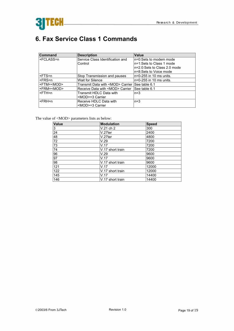
6. Fax Service Class 1 Commands
Command Description Value +FCLASS=n Service Class Identification and
Control n=0:Sets to modem mode n=1:Sets to Class 1 mode n=2.0:Sets to Class 2.0 mode n=8:Sets to Voice mode
+FTS=n Stop Transmission and pauses n=0-255 in 10 ms units. +FRS=n Wait for Silence n=0-255 in 10 ms units. +FTM=<MOD> Transmit Data with <MOD> Carrier See table 6.1 +FRM=<MOD> Receive Data with <MOD> Carrier See table 6.1 +FTH=n Transmit HDLC Data with
<MOD>=3 Carrier n=3
+FRH=n Receive HDLC Data with <MOD>=3 Carrier
n=3
The value of <MOD> parameters lists as below: Value Modulation Speed 3 V.21 ch 2 300 24 V.27ter 2400 48 V.27ter 4800 72 V.29 7200 73 V.17 7200 74 V.17 short train 7200 96 V.29 9600 97 V.17 9600 98 V.17 short train 9600 121 V.17 12000 122 V.17 short train 12000 145 V.17 14400 146 V.17 short train 14400
Page 19 of 19Revision 1.0 2003/6 From 3JTech
Research & Development
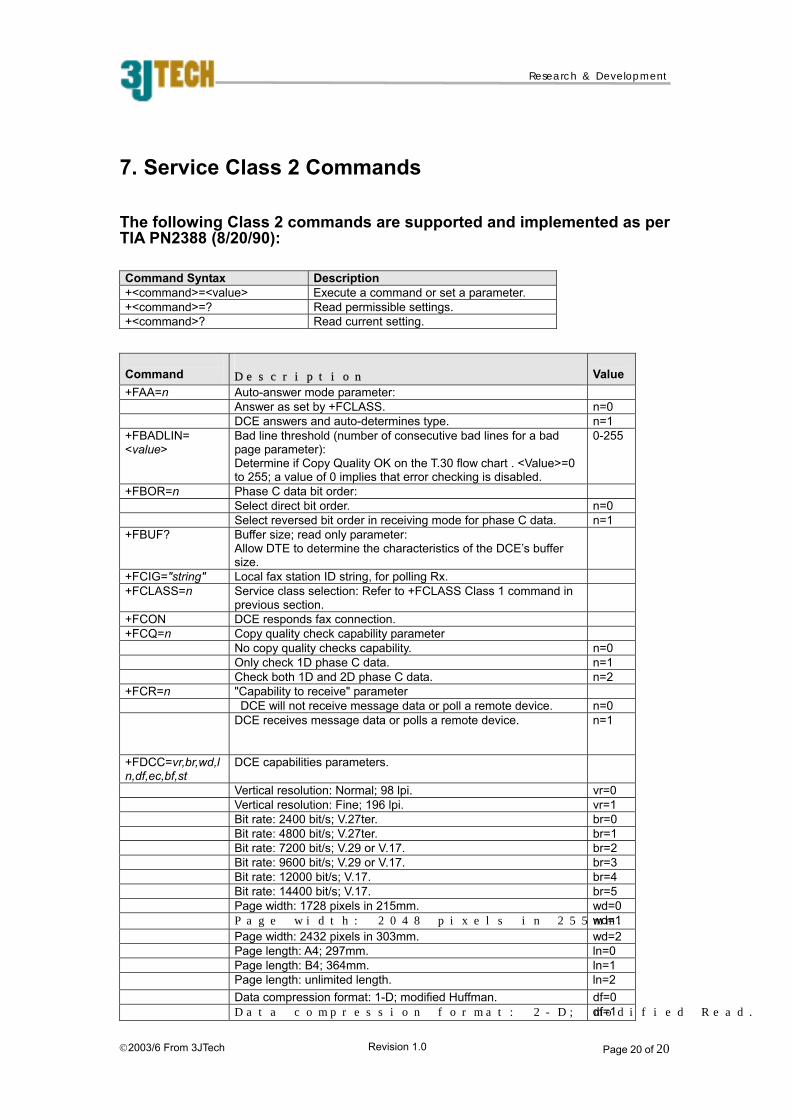
7. Service Class 2 Commands
The following Class 2 commands are supported and implemented as per TIA PN2388 (8/20/90): Command Syntax Description +<command>=<value> Execute a command or set a parameter. +<command>=? Read permissible settings. +<command>? Read current setting.
Command
Description
Value
+FAA=n Auto-answer mode parameter: Answer as set by +FCLASS. n=0 DCE answers and auto-determines type. n=1 +FBADLIN= <value>
Bad line threshold (number of consecutive bad lines for a bad page parameter): Determine if Copy Quality OK on the T.30 flow chart . <Value>=0 to 255; a value of 0 implies that error checking is disabled.
0-255
+FBOR=n Phase C data bit order: Select direct bit order. n=0 Select reversed bit order in receiving mode for phase C data. n=1 +FBUF? Buffer size; read only parameter:
Allow DTE to determine the characteristics of the DCE’s buffer size.
+FCIG="string" Local fax station ID string, for polling Rx. +FCLASS=n Service class selection: Refer to +FCLASS Class 1 command in
previous section.
+FCON DCE responds fax connection. +FCQ=n Copy quality check capability parameter No copy quality checks capability. n=0 Only check 1D phase C data. n=1 Check both 1D and 2D phase C data. n=2 +FCR=n "Capability to receive" parameter DCE will not receive message data or poll a remote device. n=0 DCE receives message data or polls a remote device.
n=1
+FDCC=vr,br,wd,ln,df,ec,bf,st
DCE capabilities parameters.
Vertical resolution: Normal; 98 lpi. vr=0 Vertical resolution: Fine; 196 lpi. vr=1 Bit rate: 2400 bit/s; V.27ter. br=0 Bit rate: 4800 bit/s; V.27ter. br=1 Bit rate: 7200 bit/s; V.29 or V.17. br=2 Bit rate: 9600 bit/s; V.29 or V.17. br=3 Bit rate: 12000 bit/s; V.17. br=4 Bit rate: 14400 bit/s; V.17. br=5 Page width: 1728 pixels in 215mm. wd=0 Page width: 2048 pixels in 255mm. wd=1 Page width: 2432 pixels in 303mm. wd=2 Page length: A4; 297mm. ln=0 Page length: B4; 364mm. ln=1 Page length: unlimited length. ln=2 Data compression format: 1-D; modified Huffman. df=0 Data compression format: 2-D; modified Read. df=1
Page 20 of 20Revision 1.0 2003/6 From 3JTech
Research & Development
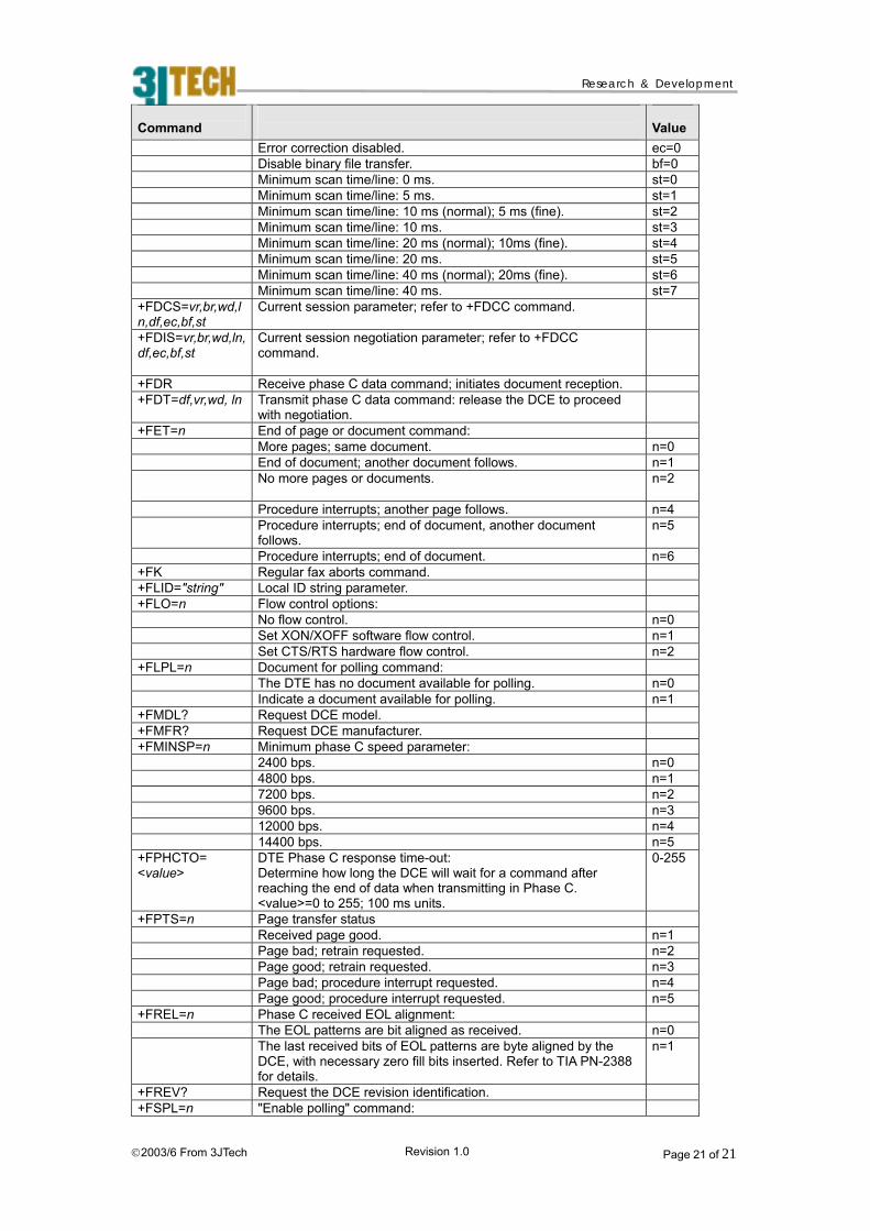
Command
Description
Value
Error correction disabled. ec=0 Disable binary file transfer. bf=0 Minimum scan time/line: 0 ms. st=0 Minimum scan time/line: 5 ms. st=1 Minimum scan time/line: 10 ms (normal); 5 ms (fine). st=2 Minimum scan time/line: 10 ms. st=3 Minimum scan time/line: 20 ms (normal); 10ms (fine). st=4 Minimum scan time/line: 20 ms. st=5 Minimum scan time/line: 40 ms (normal); 20ms (fine). st=6 Minimum scan time/line: 40 ms. st=7 +FDCS=vr,br,wd,ln,df,ec,bf,st
Current session parameter; refer to +FDCC command.
+FDIS=vr,br,wd,ln,df,ec,bf,st
Current session negotiation parameter; refer to +FDCC command.
+FDR Receive phase C data command; initiates document reception. +FDT=df,vr,wd, ln Transmit phase C data command: release the DCE to proceed
with negotiation.
+FET=n End of page or document command: More pages; same document. n=0 End of document; another document follows. n=1 No more pages or documents. n=2
Procedure interrupts; another page follows. n=4 Procedure interrupts; end of document, another document
follows. n=5
Procedure interrupts; end of document. n=6 +FK Regular fax aborts command. +FLID="string" Local ID string parameter. +FLO=n Flow control options: No flow control. n=0 Set XON/XOFF software flow control. n=1 Set CTS/RTS hardware flow control. n=2 +FLPL=n Document for polling command: The DTE has no document available for polling. n=0 Indicate a document available for polling. n=1 +FMDL? Request DCE model. +FMFR? Request DCE manufacturer. +FMINSP=n Minimum phase C speed parameter: 2400 bps. n=0 4800 bps. n=1 7200 bps. n=2 9600 bps. n=3 12000 bps. n=4 14400 bps. n=5 +FPHCTO= <value>
DTE Phase C response time-out: Determine how long the DCE will wait for a command after reaching the end of data when transmitting in Phase C. <value>=0 to 255; 100 ms units.
0-255
+FPTS=n Page transfer status Received page good. n=1 Page bad; retrain requested. n=2 Page good; retrain requested. n=3 Page bad; procedure interrupt requested. n=4 Page good; procedure interrupt requested. n=5 +FREL=n Phase C received EOL alignment: The EOL patterns are bit aligned as received. n=0 The last received bits of EOL patterns are byte aligned by the
DCE, with necessary zero fill bits inserted. Refer to TIA PN-2388 for details.
n=1
+FREV? Request the DCE revision identification. +FSPL=n "Enable polling" command:
Page 21 of 21Revision 1.0 2003/6 From 3JTech

Research & Development
Command
Description
Value
Disable polling. n=0 Enable polling. n=1
All other +F commands are not supported, but the modem will respond OK. In many cases this means "don't care." Response Value Function and Description +FCFR Confirmation. +FCIG:"string" Report remote ID response CIG. +FCON Facsimile connection response. +FCSI:"string" Report remote ID response CSI. +FDCS:vr,br,wd,ln,df,ec,bf,st
Report session parameters response; refer to +FDCC=.... command.
+FDIS:vr,br,wd,ln,df,ec,bf,st
Report session negotiation parameters response; refer to +FDCC=.... command.
+FDTC:vr,br,wd,ln,df,ec,bf,st
Report remote capabilities response; refer to +FDCC=.... command.
+FET:n Post page message response; refer to the +FET=n command.
Call termination status response. n=00 Normal and proper end of connection. n=10 Transmit error on phase A hang up code. n=20 Transmit error on phase B hang up code. n=40 Transmit error on phase C hang up code. n=50 Transmit error on phase D hang up code. n=70 Receive error on phase B hang up code. n=90 Receive error on phase C hang up code.
+FHNG:n
n=100 Receive error on phase D hang up code. +FNSC:"HEX string" Report the non-standard facilities command
frame. +FNSF:"HEX string" Report the non-standard facilities frame
response. +FNSS:"HEX string" Report the non-standard setup frame
response. +FPOLL Remote polling indication. +FPTS:n Receive page transfer status response; refer to
+FPTS=n command. +FTSI:"string" Report remote ID response TSI. +FVOICE Transition to Voice response.
Table 1. Class 2 Command Responses
Class 2 Flow Control
Flow control is necessary to match the DTE-DCE data rate to the line-signaling rate while transmitting or receiving Group 3 (T.4) data. In Class 2 fax mode, both hardware (RTS/CTS) and software (XON/XOFF) flow control are enabled.
Page 22 of 22Revision 1.0 2003/6 From 3JTech
Research & Development
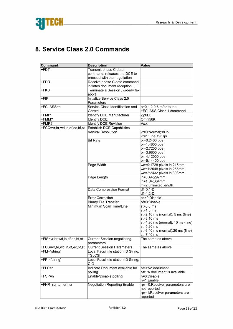
8. Service Class 2.0 Commands
Command Description Value +FDT Transmit phase C data
command: releases the DCE to proceed with the negotiation
+FDR Receive phase C data command: initiates document reception
+FKS Terminate a Session , orderly fax abort
+FIP Initialize Service Class 2.0 Parameters
+FCLASS=n Service Class Identification and Control
n=0,1,2.0,8;refer to the +FCLASS Class 1 command
+FMI? Identify DCE Manufacturer ZyXEL +FMM? Identify DCE Omni56K +FMR? Identify DCE Revision Vx.x
Establish DCE Capabilities Vertical Resolution vr=0:Normal;98 lpi
vr=1:Fine;196 lpi Bit Rate br=0:2400 bps
br=1:4800 bps br=2:7200 bps br=3:9600 bps br=4:12000 bps br=5:14400 bps
Page Width wd=0:1728 pixels in 215mm wd=1:2048 pixels in 255mm wd=2:2432 pixels in 303mm
Page Length ln=0:A4;297mm ln=1:B4;364mm ln=2:unlimited length
Data Compression Format df=0:1-D df=1:2-D
Error Correction ec=0:Disable
+FCC=vr,br,wd,ln,df,ec,bf,st
Binary File Transfer bf=0:Disable Minimum Scan Time/Line st=0:0 ms
st=1:5 ms st=2:10 ms (normal); 5 ms (fine) st=3:10 ms st=4:20 ms (normal); 10 ms (fine) st=5:20 ms st=6:40 ms (normal);20 ms (fine) st=7:40 ms
+FIS=vr,br,wd,ln,df,ec,bf,st Current Session negotiating parameters
The same as above
+FCS=vr,br,wd,ln,df,ec,bf,st Current Session Parameters The same as above +FLI=”string” Local Facsimile station ID String,
TSI/CSI
+FPI=”string” Local Facsimile station ID String, CIG
+FLP=n Indicate Document available for polling
n=0:No document n=1:A document is available
+FSP=n Enable/Disable polling n=0:Disable n=1:Enable
+FNR=rpr,tpr,idr,nsr Negotiation Reporting Enable rpr= 0:Receiver parameters are not reported rpr=1:Receiver parameters are reported
Page 23 of 23Revision 1.0 2003/6 From 3JTech

Research & Development
tpr= 0:Transmitter parameters are not reported tpr=1:Transmitter parameters are reported idr= 0: ID Strings are not reported idr=1: ID Strings are reported nsr= 0:Non-standard frames are not reported nsr= 1:Non-standard frames are reported
+FIE=n Procedure Interrupt parameter n=0:Disable n=1:Enable
+FPS=n Page Transfer Status n=1:Received page is good n=2:Page is bad; retrain is requested n=3:Page is good; retrain is requested n=4:Page is bad; procedure interrupt is requested n=5:Page is good; procedure interrupt is requested
+FLO=n Flow Control Select n=0:No flow control n=1:Sets XON/ XOFF software flow control n=2:Sets CTS/RTS hardware flow control
+FPR=n Serial Port Rate Control n=0:Automatic DTE rate detection by the DCE n>0:Serial rate is fixed at the value multiplied by 2400 bps
+FBO=n Phase C Data Bit Order n=0:Selects direct bit order n=1:Selects reversed bit order
+FEA=n Phase C Received EOL alignment
n=0:EOL patterns are as received
+FCR=n Capability to Receive n=0:Not receive message data or poll a remote device n=1: Receives message data or poll a remote device
+FCQ=<rq>,<tq> Copy Quality disable/enable rq= 0:Receive copy quality check is disable rq=1:Receive copy quality check is enable tq= 0:Transmit copy quality check is disable tq=1:Transmit copy quality check is enable
+FRQ=pql,cbl Receive Quality Thresholds pgl= 0-64h:Specifies the percentage of good lines cbl= 0-ffh:Specifies the maximum tolerable number of consecutive bad lines
+FAA=n Adaptive Answer Mode n=0:Answers as set by +FCLASS n=1:Answers and auto-determines the call type
+FCT=n Phase C Timeout n=0-ffh,1 sec units +FMS=n Minimum Phase C Speed n=0:2400 bps
n=1:4800 bps n=2:7200 bps n=3:9600 bps n=4:12000 bps n=5:14400 bps
+FBS? Buffer Size 512,256
Page 24 of 24Revision 1.0 2003/6 From 3JTech
Research & Development
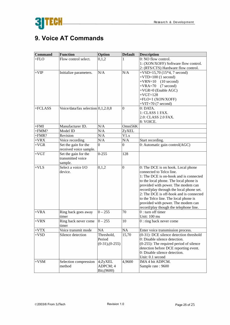
9. Voice AT Commands
Command Function Option Default Description +FLO Flow control select. 0,1,2 1 0: NO flow control.
1: (XON/XOFF) Software flow control. 2: (RTS/CTS) Hardware flow control.
+VIP Initialize parameters. N/A N/A +VSD=15,70 (15*4, 7 second) +VTD=100 (1 second) +VRN=10 (10 second) +VRA=70 (7 second) +VGR=0 (Enable AGC) +VGT=128 +FLO=1 (XON/XOFF) +VIT=70 (7 second)
+FCLASS Voice/data/fax selection 0,1,2.0,8 0 0: DATA. 1: CLASS 1 FAX. 2.0: CLASS 2.0 FAX. 8: VOICE.
+FMI Manufacturer ID. N/A Omni56K +FMM? Model ID N/A ZyXEL +FMR? Revision N/A V1.x +VRX Voice recording N/A N/A Start recording. +VGR Set the gain for the
received voice sample.0 0 0: Automatic gain control(AGC)
+VGT Set the gain for the
transmitted voice sample.
0-255 128
+VLS Select a voice I/O device.
0,1,2 0 0: The DCE is on hook. Local phone connected to Telco line. 1: The DCE is on-hook and is connected to the local phone. The local phone is provided with power. The modem can record/play through the local phone set. 2: The DCE is off-hook and is connected to the Telco line. The local phone is provided with power. The modem can record/play though the telephone line.
+VRA Ring back goes away timer
0 – 255 70 0 : turn off timer Unit: 100 ms
+VRN Ring back never come timer
0 – 255 10 0 : ring back never come
+VTX Voice transmit mode NA NA Enter voice transmission process. +VSD Silence detection Threshold,
Period (0-31),(0-255)
15,70 (0-31): DCE silence detection threshold 0: Disable silence detection. (0-255): The required period of silence detection before DCE reporting event. 0: Disable silence detection. Unit: 0.1 second
+VSM Selection compression method
4;ZyXEL ADPCM; 4 Bit;(9600)
4,9600 IMA 4 bit ADPCM. Sample rate : 9600
Page 25 of 25Revision 1.0 2003/6 From 3JTech

Research & Development
+VTS= [x,y,x]
Dual Tone generation [[x,y,z]: x: 0-3000 Hzy: 0-3000 Hzz: 0- 1000 (in 10ms)
NA [x,y,z]: x: first frequency y: second frequency z: duration in 10ms.
+VTS = {x,z}
DTMF tone generation {x,y} x:0-9,A-D,*,#y:0-1000
NA {x,y} x: DTMF y: duration in 0.1 sec.
+VTS = x
DTMF tone generation {x} x:0-9,A-D,*,#
NA x: Default duration: +VTD setting.
+VTD Default DTMF tone generation duration.
0-255 50 Unit: 0.01 second.
+VIT Inactivity timer. 0-255 70 Unit: 0.1 second.
Note1: The voice function can be determined by WinFax Pro 9.0 except speaker phone function. Note2: Above voice command set is the subset of G2 voice command set except the following command: AT+VLH=? Inquire hook status. AT+VNH=<hook> Enable/disable automatic hang-up function. AT+VDD=<dds>,<ddi> Set DTMF detection threshold and required period. AT+VSY=<timer> Set recording resync timer. Note3: The d evice selection command “+VLS” is different from IS101 and “#” voice command set. This problem is associated with speaker phone function.
Response Code Description
<DLE>0 - <DLE>9
<DLE>*,<DLE>#
<DLE>A-<DLE>D
DTMF
<DLE>a Answer Tone
<DLE>b Busy
<DLE>c Calling Tone
<DLE>d Dial tone
<DLE>e European Data Modem Calling Tone
<DLE>f Bell Answer Tone
<DLE>h Hang Hand set
<DLE>o Overrun
<DLE>q Quiet , silence detected with voice received before,
<DLE>s Silence, silence detected with never received voice.
<DLE>t Handset off-Hook
<DLE>u Under run
<DLE>T Timing Mark
<DLE><ETX> End of stream
Page 26 of 26Revision 1.0 2003/6 From 3JTech

Research & Development
10. S-Register Description
In most bit-mapped S-registers, the default bit value is 0. Non-0 default values are followed by an asterisk. In some cases, default values are shown in the reference column preceded by +. Some bits are reserved for factory use and should not be changed.
10.1 Basic S-Registers "ATSn=x"
Command Function & Description +Ref. S0= Set the number of rings on which the modem will answer. 0 value
disable auto-answer +000
S1= Counts and stores number of rings from an incoming call +000 S2= Define escape code character, default ‘+’ (43 dec.). A value of 128-255
disables the escape code +043
S3= Define ASCII Carriage Return +013 S4= Define ASCII Line Feed +010 S5= Define ASCII Backspace. A value of 128-255 disables the Backspace
key’s delete function +008
S6= Set the number of seconds the modem waits before dialing if ‘X0’ or ‘X1’ is selected. If a setting of ‘X2’ to ‘X7’ is selected, the modem will dial as soon as it detects a dial tone. This register also sets the time-out interval for the “W” dial modifier to wait for the dial tone. (See also S41b4)
+003
S7= Set duration, in number of seconds modem waits for a carrier +060 S8= Set duration, in seconds, for pause (,) option in Dial command and
pause between command re-executions for Repeat (>) command +002
S9= Set duration, in tenths of a second of remote carrier signal before recognition (Ignored if in non-FSK or half-duplex operation)
+006
S10= Set duration, in tenths of a second, modem waits after loss of carrier before hanging up
+007
S11= Set duration and spacing, in milliseconds, of dialed Touch-Tones +070
10.2 Extended S-Registers "ATSn=x"
Command bit dec hex Function and description Ref. S13= bit dec hex Bit-mapped register +000 1 2 2 Capture modem manufacturer information during
V.42 handshake, can be displayed at ATI2 <Last Speed/Protocol> line if available (‘Flash’ or ‘ ZyXEL’ stands for ZyXEL connection)
S14= bit dec hex Bit-mapped register: +002 1 0 0 Grant Remote Digital Loop-back test request &T4 2 2 Deny Remote Digital Loop-back test &T5 S15= bit dec hex Bit-mapped register +066 0,1 0 0 Even parity
Page 27 of 27Revision 1.0 2003/6 From 3JTech
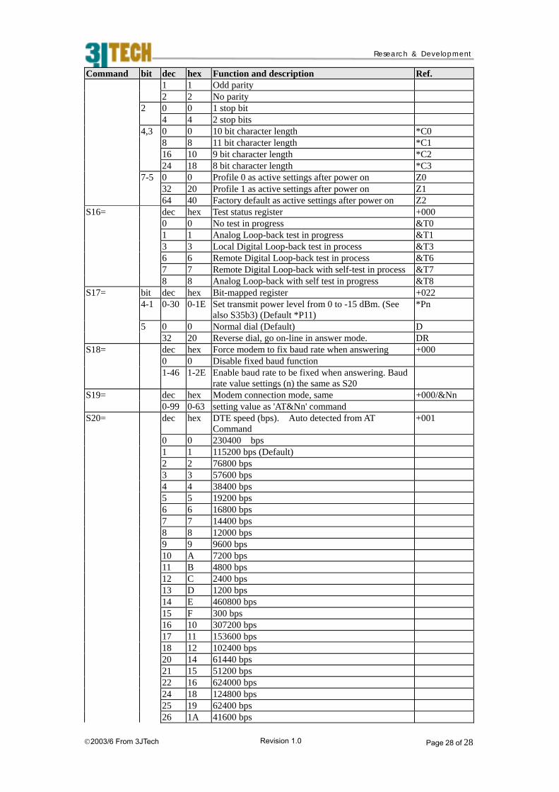
Research & Development
Command bit dec hex Function and description Ref. 1 1 Odd parity 2 2 No parity 2 0 0 1 stop bit 4 4 2 stop bits 4,3 0 0 10 bit character length *C0 8 8 11 bit character length *C1 16 10 9 bit character length *C2 24 18 8 bit character length *C3 7-5 0 0 Profile 0 as active settings after power on Z0 32 20 Profile 1 as active settings after power on Z1 64 40 Factory default as active settings after power on Z2 S16= dec hex Test status register +000 0 0 No test in progress &T0 1 1 Analog Loop-back test in progress &T1 3 3 Local Digital Loop-back test in process &T3 6 6 Remote Digital Loop-back test in process &T6 7 7 Remote Digital Loop-back with self-test in process &T7 8 8 Analog Loop-back with self test in progress &T8 S17= bit dec hex Bit-mapped register +022 4-1 0-30 0-1E Set transmit power level from 0 to -15 dBm. (See
also S35b3) (Default *P11) *Pn
5 0 0 Normal dial (Default) D 32 20 Reverse dial, go on-line in answer mode. DR S18= dec hex Force modem to fix baud rate when answering +000 0 0 Disable fixed baud function 1-46 1-2E Enable baud rate to be fixed when answering. Baud
rate value settings (n) the same as S20
S19= dec hex Modem connection mode, same +000/&Nn 0-99 0-63 setting value as 'AT&Nn' command S20= dec hex DTE speed (bps). Auto detected from AT
Command +001
0 0 230400 bps 1 1 115200 bps (Default) 2 2 76800 bps 3 3 57600 bps 4 4 38400 bps 5 5 19200 bps 6 6 16800 bps 7 7 14400 bps 8 8 12000 bps 9 9 9600 bps 10 A 7200 bps 11 B 4800 bps 12 C 2400 bps 13 D 1200 bps 14 E 460800 bps 15 F 300 bps 16 10 307200 bps 17 11 153600 bps 18 12 102400 bps 20 14 61440 bps 21 15 51200 bps 22 16 624000 bps 24 18 124800 bps 25 19 62400 bps 26 1A 41600 bps
Page 28 of 28Revision 1.0 2003/6 From 3JTech

Research & Development
Command bit dec hex Function and description Ref. 27 1B 31200 bps 28 1C 24960 bps 29 1D 20800 bps 46 2E 921600 bps Note: Only the speeds up to S20=15 are supported by auto speed detection. S21= bit dec hex Bit mapped register +178 0 0 0 Maintain non-error control connection when modem
error control handshake fails *E0
1 1 Drop connection when modem error control handshake fails (default)
*E1
1-2 0 0 Speaker is always OFF M0 2 2 Speaker is ON until carrier is detected (default) M1* 4 4 Speaker is always ON M2 6 6 Speaker is ON after last digit is dialed out until
carrier detected M3
3 0 0 DSR is always ON (default) &S0 8 8 According to CCITT (see also S44.4, S41.5) &S1 4 0 0 CD is always ON &C0 16 10 CD tracks presence of data carrier (see also S38.3)
(default) &C1
5 0 0 CTS Follows RTS in synchronous mode. Response delay set in S26
&R0
32 20 Ignore RTS (CTS always ON) in synchronous mode. (Default)
&R1
6-7 0 0 Assume DTR always On &D0 64 40 108.1, DTR OFF-ON transition causes dial of the
default number &D1
128 80 108.2 Data Terminal Ready, DTR OFF causes the modem to hang up and return to command state (default)
&D2
192 C0 108.2, DTR OFF causes the modem to hang up and reset the modem to profile 0 after DTR dropped
&D3
S23= bit dec hex Bit mapped register +105 0 0 0 Command echo disabled E0 1 1 Command echo enabled (default) E1 1 0 0 Tone dial. (Default) T 2 2 Pulse dial. P 2 0 0 Pulse dial make/break ratio = 39% / 61% (default) &P0 4 4 Pulse dial make/break ratio = 33% / 67% &P1 3-5 0 0 ATX0 (See result code table) X0 8 8 ATX1 X1 16 10 ATX2 X2 24 18 ATX3 X3 32 20 ATX4 X4 40 28 ATX5, error control result code is enabled (Default) X5 48 30 ATX6, error control result code is enabled X6 56 38 ATX7, error control result code is enabled X7 6 0 0 Display result code in numeric format (see S35.7) V0 64 40 Display result code in verbose format V1 7 0 0 Modem returns result code Q0 128 80 Modem does not return result code (see also S40.1) Q1 S24= bit dec hex Bit mapped register +067 6-4 16-11
2 10-70 Speaker volume control, increments of 16 in decimal
value L0-7
S25= 0-255 0-FF Specify the time delay that DTR signal needs to be OFF before it will be recognized, in 10 ms units. If
+000
Page 29 of 29Revision 1.0 2003/6 From 3JTech
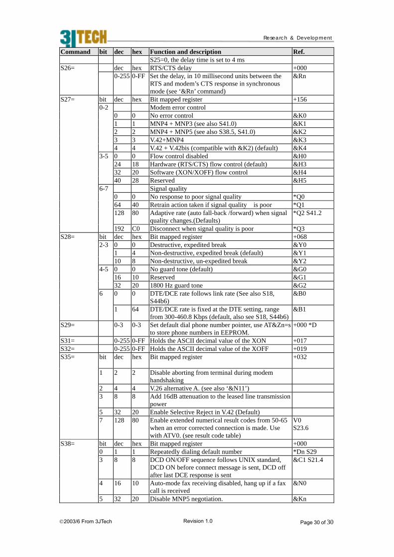
Research & Development
Command bit dec hex Function and description Ref. S25=0, the delay time is set to 4 ms
S26= dec hex RTS/CTS delay +000 0-255 0-FF Set the delay, in 10 millisecond units between the
RTS and modem’s CTS response in synchronous mode (see ‘&Rn’ command)
&Rn
S27= bit dec hex Bit mapped register +156 0-2 Modem error control 0 0 No error control &K0 1 1 MNP4 + MNP3 (see also S41.0) &K1 2 2 MNP4 + MNP5 (see also S38.5, S41.0) &K2 3 3 V.42+MNP4 &K3 4 4 V.42 + V.42bis (compatible with &K2) (default) &K4 3-5 0 0 Flow control disabled &H0 24 18 Hardware (RTS/CTS) flow control (default) &H3 32 20 Software (XON/XOFF) flow control &H4 40 28 Reserved &H5 6-7 Signal quality 0 0 No response to poor signal quality *Q0 64 40 Retrain action taken if signal quality is poor *Q1 128 80 Adaptive rate (auto fall-back /forward) when signal
quality changes.(Defaults) *Q2 S41.2
192 C0 Disconnect when signal quality is poor *Q3 S28= bit dec hex Bit mapped register +068 2-3 0 0 Destructive, expedited break &Y0 1 4 Non-destructive, expedited break (default) &Y1 10 8 Non-destructive, un-expedited break &Y2 4-5 0 0 No guard tone (default) &G0 16 10 Reserved &G1 32 20 1800 Hz guard tone &G2 6 0 0 DTE/DCE rate follows link rate (See also S18,
S44b6) &B0
1 64 DTE/DCE rate is fixed at the DTE setting, range from 300-460.8 Kbps (default, also see S18, S44b6)
&B1
S29= 0-3 0-3 Set default dial phone number pointer, use AT&Zn=s to store phone numbers in EEPROM.
+000 *D
S31= 0-255 0-FF Holds the ASCII decimal value of the XON +017 S32= 0-255 0-FF Holds the ASCII decimal value of the XOFF +019 S35= bit dec hex Bit mapped register +032
1 2 2 Disable aborting from terminal during modem
handshaking
2 4 4 V.26 alternative A. (see also ‘&N11’) 3 8 8 Add 16dB attenuation to the leased line transmission
power
5 32 20 Enable Selective Reject in V.42 (Default) 7 128 80 Enable extended numerical result codes from 50-65
when an error corrected connection is made. Use with ATV0. (see result code table)
V0 S23.6
S38= bit dec hex Bit mapped register +000 0 1 1 Repeatedly dialing default number *Dn S29 3 8 8 DCD ON/OFF sequence follows UNIX standard,
DCD ON before connect message is sent, DCD off after last DCE response is sent
&C1 S21.4
4 16 10 Auto-mode fax receiving disabled, hang up if a fax call is received
&N0
5 32 20 Disable MNP5 negotiation. &Kn
Page 30 of 30Revision 1.0 2003/6 From 3JTech
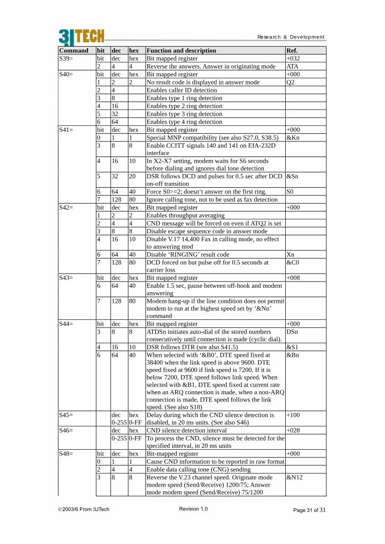
Research & Development
Command bit dec hex Function and description Ref. S39= bit dec hex Bit mapped register 2 4 Reverse the answers. Answer in originating mode ATA S40= dec hex Bit mapped register +000 1 2 2 Q2 2 Enables caller ID detection
3 8 Enables type 1 ring detection 4 16 Enables type 2 ring detection 32 Enables type 3 ring detection 6 64 S41= bit hex Bit mapped register +000
0 1 1 Special MNP compatibility (see also S27.0, S38.5) 3 8 Enable CCITT signals 140 and 141 on EIA-232D
interface
16 10 In X2-X7 setting, modem waits for S6 seconds before dialing and ignores dial tone detection
5 32 20 &Sn
6 40 Force S0>=2; doesn‘t answer on the first ring. S0 7 128 80 Ignore calling tone, not to be used as fax detection
S42= bit dec Bit mapped register +000 2 2 Enables throughput averaging 2 4 4 3 8 Disable escape sequence code in answer mode
4 16 10 Disable V.17 14,400 Fax in calling mode, no effect to answering mod
6 64 Disable ‘RINGING’ result code Xn 128 80 DCD forced on but pulse off for 0.5 seconds at
carrier loss &C0
S43= bit dec hex +008 6 40 Enable 1.5 sec, pause between off-hook and modem
answering
7 128 80 Modem hang-up if the line condition does not permit modem to run at the highest speed set by ‘&Nn’ command
S44= bit dec Bit mapped register +000 8 8 ATDSn initiates auto-dial of the stored numbers
consecutively until connection is made (cyclic dial). DSn
4 16 10 &S1 6 40 When selected with ‘&B0’, DTE speed fixed at
38400 when the link speed is above 9600. DTE speed fixed at 9600 if link speed is 7200. If it is below 7200, DTE speed follows link speed. When selected with &B1, DTE speed fixed at current rate when an ARQ connection is made, when a non-ARQ connection is made, DTE speed follows the link speed. (See also S18)
&Bn
dec 0-255
hex Delay during which the CND silence detection is disabled, in 20 ms units. (See also S46)
+100
S46= dec hex CND silence detection interval +028 0-255 0-FF
S48= bit hex Bit-mapped register +000 0 1 1 Cause CND information to be reported in raw format
2 4 Enable data calling tone (CNG) sending 8 8 Reverse the V.23 channel speed. Originate mode
modem speed (Send/Receive) 1200/75; Answer mode modem speed (Send/Receive) 75/1200
&N12
+032 4
bit No result code is displayed in answer mode
4
5
Enables type 4 ring detection dec
&Kn 8
4
DSR follows DCD and pulses for 0.5 sec after DCD on-off transition
64
hex 1
CND message will be forced on even if ATQ2 is set 8
40 7
Bit mapped register 64
hex 3
DSR follows DTR (see also S41.5) 64
S45= 0-FF
To process the CND, silence must be detected for the specified interval, in 20 ms units
dec
4 3
Page 31 of 31Revision 1.0 2003/6 From 3JTech
Research & Development
Command bit dec hex Function and description Ref. 4 16 10
S52= bit hex Bit-mapped register +000 7 0 0 Select ‘Mark’ as the first signal of the V.23
handshaking sequence (Default) 128 Select ‘Space’ as the first signal of the V.23
handshaking sequence &N12
S56= dec hex +000 0-255 0-FF
(Work with &D1 command) DTR ON will have the modem dial the default number and DTR OFF will have the modem hang-up and reset to profile 0. When the modem is idle (waiting for command), it will not dial any number when DTR changes from ON to OFF
dec &N12
80
Hook flash detect time, in units of 10ms, country specific
S57= bit dec hex Bit-mapped register +016 16 10 Enables the reporting of Class 1 capability in the
response to +FCLASS=?
S59= bit dec hex 0 0 Not display
4 16 10 Display the expected values automatically when using the interrupt mechanism.
5 32 Will put 3 chars
S-register bit number, 'b', used in 'ATSr.b=n' and 'ATSr.b=?' dec Decimal value, 'x', used in 'ATSn=x' hex Equivalent Hexadecimal value.
+nnn Note: 'AT' is omitted when an AT command is referred to in the 'Reference'
column..
4
Display the expected values 0
20
Bit
Factory default when listed in 'Reference' column.
Page 32 of 32Revision 1.0 2003/6 From 3JTech

Research & Development
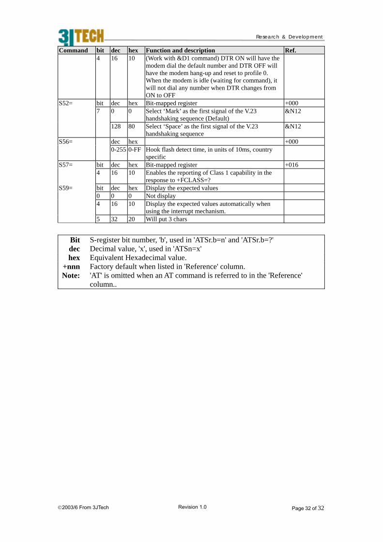
11. Current Detect Specification AT Commands
Revise: - Change all the naming of modem interrupt-related commands AT#I<n> -> AT%I<n> AT#S<n> -> AT%X<n>
- The modem interrupts coming from "Line status change" and "Carrier loss " may be identified by AT%I3 - The voltage setting and current setting sync with the table with
Modulation: V90/V.34/V.32bis/V.32/V.22bis/V.23/V.21/Bell212A Link layer: MNP3/4/5, V42/V42bis
11.2 Receive Sensitivity
11.3 Transmit Level
Command: AT*P<n> Parameter: <n>: 8 to 25, set the transmit power from -8 dBm to –25 dBm
ERROR (i.e. Invalid value) Default value: -11 dBm
11.4 Return Loss
- Allow the host to change the polling time via AT%X2
11.1 Protocols
-24 +/- 2 dBm
Response: OK (i.e. Success)
300 – 3400 Hz: > 10 dB
Page 33 of 33Revision 1.0 2003/6 From 3JTech
Research & Development
11.5 Dialing Type
AT&P0: Pulse dial Make/break ratio - 39/61 AT&P1: Pulse dial Make/break ratio - 33/67 Pulses per second: 10
11.6 Calling Progress Monitors
Dial tone: - ATD command will detect the dial tone then dial the number. - If the dial tone is not detected in the time defined by the S6 register (default 3 seconds), then respond “NO DIALTONE”
Busy tone: - If the busy tone is detected, then respond “BUSY”. Ring back tone: - If the ring back tone is detected, then respond “RINGING”
11.7 DTMF Tone Level
High-frequency group: -8 +/- 2 dBm Low-frequency group: -10 +/- 2 dBm
The character format is N81, and supports the hardware flow control.
11.9 Modem Interrupt
Provide the following customization commands to define the thresholds used to issue an interrupt to the host CPU when the line voltage / current is changed. And also provide some commands to query the line status.
11.8 UART Interface
Page 34 of 50Revision 1.0 2003/6 From 3JTech
Research & Development
11.9.1 Detection mode setting
Description: Set the different detection mode used to issue an interrupt when the line voltage/current is changed. Command: AT%X0=<On Hook Detection Mode>, <Off Hook Detection mode>
Parameter :< On Hook Detection mode>: 0: Issue an interrupt when the line voltage difference exceeds the
defined threshold (ref to 9.2). 1: Issue an interrupt when the line voltage absolute value exceeds
the defined threshold (ref to 9.2). 2: Disable the line voltage detection.
<Off Hook Detection mode>: 0: Issue an interrupt when the line current difference exceeds the
defined threshold (ref to 9.2).
2: Disable the line current detection. ? : Query the current setting Response:
(2) <On Hook Detection mode>,<Off Hook Detection mode> OK : Response for query setting. (3) ERROR: Error Setting
11.9.2 Threshold setting
Command: AT%X1=<On hook voltage thresh.>, < Off hook current thresh.> AT%X1=?
From 0 to 31, this applies to both of the differential and absolute voltage threshold. Please refer to Table 9.1.for the scale transformation. < Off hook current thresh.>
From 0 to 31, this applies to both of the differential and absolute
AT%X0=?
1: Issue an interrupt when the line current absolute value exceeds the defined threshold (ref to 9.2).
(1) OK : Setting Successfully.
Default: 1,1
Parameter: <On hook voltage thresh.>
Page 35 of 50Revision 1.0 2003/6 From 3JTech

Research & Development
current threshold. Please refer to Table 9.2.for the scale transformation.
Response: (1) OK : Setting Successfully (2) <On hook voltage thresh.>, <Off hook current thresh.> OK : Response for query setting.
Default: 5, 2 - For the differential mode 12, 10 - For the absolute mode
?: Query the current setting
(2) ERROR: Error setting
Table 11.9.1: Voltage translate Table
Command
Value 0 1 2 4 5 6 8 9 10 12 13 14 16 17 18 20 21 22 24 25 26 28 29 30
Voltage
(Volt) 03 05 08 12 15 17 21 23 25 30 32 34 39 41 44
3 7 11 15 19 23 27 31
00 10 19 27 36 46 48 51 53 55 57 60 62 64 66 68
Command
Value 0
70
Table 11.9.2: Current translate Table (FCC) 1 2 3 4 5 6 7 8 9 10 11 12 14 15 16 18 19 20 22 23 24 26 27 28 30 31
(mA) 00 12 18 21 24 30 33 36 42 45 48 54 57 60 66 69 72 78 81 84 90 93 96 99
Command
Value 0 1 3 4 5 7 8 9 10 11 13 14 15 17 18 19 21 22 23 25 26 27 29 30 31
Voltage
(mA) 00 15 18 21 27 30 33 39 40 42 45 46 48 51 52 54 57 58 60 60 60 60 60 60
11.9.3 Polling time setting
Description: Set the polling time used to detect the status change on the line. Command: AT%X2=<POLL_TIME>
Parameter: <POLL_TIME>: Polling interval in 10 ms unit. ? : Query the current setting
13 17 21 25 29
15 27 39 51 63 75 87 99Voltage
Table 11.9.3: Current translate Table (CTR21) 2 6 12 16 20 24 28
12 24 36 43 49 55 60 60
AT%X2=?
Page 36 of 50Revision 1.0 2003/6 From 3JTech

Research & Development
Response: (1) OK : Setting Successfully. (2) <POLL_TIME> OK : Response for query setting. (3) ERROR : Error setting.
11.9.4 Line status query
Description: Query the line status Command: AT%I0
Response: <Event> 0 – Line de-attached, Nothing happens. 1 - Line voltage difference / absolute value are below the threshold
defined in 9.2.
3 - Line current difference / absolute value are below the threshold defined in 9.2 (Note: when set S59=32, Modem will put 3 chars 47 47 47 to alert extra. Otherwise you can disable it by set S59 = 0)
4 - Line current difference / absolute value is over the threshold defined in 9.2
OK
Description: Query the RJ11 status Command: AT%I1 Parameter: None
0 - No phone line is attached. 1 – A phone line is attached. OK
Description: Query the voltage/current value, and the value type, absolute or
Default: 100 (1 second)
Parameter: None
2 - Line voltage difference / absolute value are over the threshold defined in 9.2.
11.9.5 RJ11 status query
Response: <Line status>
11.9.6 Voltage/Current value query
Page 37 of 50Revision 1.0 2003/6 From 3JTech

Research & Development
differential, depends on the detection mode you set. Command: AT%I2 Parameter: None
/ Table 9.2 for this value. OK
11.9.7 Event status query
Command: AT%I3 Parameter: None Response: <Interrupt Status>: The interrupt reasons are as follows. The status is automatically cleared after read.
1: The modem interrupt is caused by the “Line status change”, And the detailed reason can be read from AT%I0. 2: The modem interrupt is caused by the “Carrier Loss”.
11.10 Reset Signal Pin
Allow active signal pin indicating the modem module to reset.
11.11 Escape Signal Pin
A signal high on the pin “ESC” forces the modem enter the command mode. Then the modem will respond an “OK” string and enter the escape state. “ATO” command will let the modem return to the data state.
12.1 Power on self test A test for basic components whenever power on.
Response: <Value>. This value is an unsigned value, and please refers to Table 9.1
Description: Query the event status.
0: Nothing happens or be cleared.
OK
11.12 Diagnostics
Page 38 of 50Revision 1.0 2003/6 From 3JTech

Research & Development
12.2 Analog loop back test AT&T1, a modem connect test via an analog loop back path.
AT&T8, an analog loop back test with a test pattern sent/received by the modem itself.
11.13 Configurable Parameters
Value range Unit Description
%1 Reserved Reserved
%2 Reserved Reserved
%3 Reserved Reserved
%4 Reserved Reserved
<10 - 255> 10 ms Dial-tone detection time
%6 Reserve Reserve
%7 <0 – 255> Factory default for S6
%8 1 sec Factory default for S7
<0 – 255> 1 ms Factory default for S11
%10 <0 – 255> 1 sec
%11 <0 – 255> Redial interval for the last time, RDT2
%12 NA Number of redial using T1 (RDN1), RDN1 =
RDN2 – 1
<0 – 15> NA Maximum number of redial, RDN2
%14 <0 – 15> 1 dB
%15 <0 – 15> DTMF low-group power, -11 dBm+(-8 to 7) dB
%16 NA Pulse per second for pulse dial
0: 10 PPS, 1: 16 PPS, 2: 20 PPS, 3: Disable.
%17 <0 – 1> 0: 39/61 Factory default Make / Break ratio
%18 On / Off Detect busy tone before dial.
Reserve Reserve
%20 <0 – 3> Dial pulse inter-digit delay, from 700 ms to 1000
ms
%21 0: (Digit)
pulses
Pulses of each digit
12.3 Analog loop back with self test
PTT ID
Reserved
Reserved
Reserved
Reserved
%5
Reserve
1 sec
<0 – 255>
%9
Redial interval for the first several times, RDT1
1 sec
<0 – 15>
%13
DTMF high-group power, -9dBm+(-8 to 7 )dB
1 dB
<0 – 3>
1: 33/67
<1 / 0>
%19 Reserve
700 ms to
1000 ms
step: 100 ms
<0 – 1>
Page 39 of 50Revision 1.0 2003/6 From 3JTech
Research & Development
1: (Digit+1)
%22 ms Flash time. 0: 500 ms, 1: 300 ms, 2: 100 ms,
3:120 ms
%23 <1 / 0> On / Off
%24 <1 / 0> DAA setting for CTR21
%25 50 ms to
800 ms
step: 50 ms
Delay time to OFF_Hook.
%26 <1 / 0> On / Off
%27 <0 – 127> DAA configuration
%28 NA Country code for CPM initialization
<1 / 0> On / Off DAA setting for DTMF CID detection
%30 Reserved Reserved
pulses
<0 – 3>
Calling tone enable.
Yes / No
<0 – 15>
Enable dial-up line transmit power adjustment.
NA
<0 – 255>
%29
Reserved
%31 <1 / 0> On / Off Enable "RING" reporting at the rising edge of ring
<1 / 0> On / Off Use the half-wave rectifier for Si3034 setting
%33 <1 / 0> On / Off
%34 Reserved Reserved
%35 Reserved Reserved
Reserved Reserved Reserved
%32
CID Polarity setting.
Reserved
Reserved
%36
Page 40 of 50Revision 1.0 2003/6 From 3JTech

Research & Development
12. The Specification with Si3044
12.1 UModem Specification:
However, Si3044 cannot detect the parallel phone directly. It can only measure the line voltage when the line is on-hook. And measure the loop current when the line is off-hook. It will judge the parallel phone is off-hook according to some of pre-set threshold. Refer to section 0 for details.
The main specification is that when bit2 of S63 is enabling, the modem is allowed to use line when the parallel phone is not in use. (Flow chart is as the following figure).
Oldfunction
Modem standby
Modem start dial
Check parallelphone
Ask to connect
Current state
Modem On-hookSend errormessage
Parallel phoneoff-hook
Parallel phoneon-hook
Parallel phoneoff-hook
Use parallelphone
Parallel phoneoff-hook
Use modem
Parallel phoneon-hook
Modem on-hook
S63.2
Enable bit=1
Disable bit=0
Page 41 of 50Revision 1.0 2003/6 From 3JTech
Research & Development
12.2 Additional command set.
Provide the following customization commands to define the thresholds used to determine the parallel line is off-hook or not. And also provide some commands to query the line status.
12.2.1 Detection mode setting
Description: Set the different detection mode used to detect the parallel phone is off-hook or not. Command: AT%X0=<On Hook Detection Mode>, <Off Hook Detection mode> AT%X0=? Parameter: <On Hook Detection mode>:
0: Assume parallel phone is off-hook when the line voltage difference exceeds the defined threshold (ref to0).
1: Assume parallel phone is off-hook when the line voltage exceedsthe defined threshold (ref to0).
2: Disable the line voltage detection. <Off Hook Detection mode>:
0: Assume parallel phone is off-hook when the line current difference exceeds the defined threshold (ref to 0).
1: Assume parallel phone is off-hook when the line current exceeds the defined threshold (ref to 0).
2: Disable the line current detection. ? Query the current setting
Response: (1) OK : Setting Successfully. (2) <On Hook Detection mode>,<Off Hook Detection mode>
OK Response for query setting. (3) ERROR : Error Setting
Default: 1,1
12.2.2 Threshold setting
Command: AT%X1=<On hook voltage thresh. >, < Off hook current thresh. > AT%X1=? Parameter: <On hook voltage thresh. >
0 to 31, which applies to both of the differential and absolute voltage threshold. Please refer to Table 12.2.1.for the scale transformation.
< Off hook current thresh. >
Page 42 of 50Revision 1.0 2003/6 From 3JTech

Research & Development
0 to 31, which applies to both of the differential and absolute current threshold. Please refer to Table 12.2.2.for the scale transformation.
? Query the current setting
Response: (1) OK : Setting Successfully (2) <On hook voltage thresh. >, <Off hook current thresh. >
OK : Response for query setting. (3) ERROR : Error setting
Default: 5, 2 - For the differential mode 12,10 - For the absolute mode
Table 12.2.1: Voltage translates Table Command
Value 0 1 2 3 4 5 6 7 8 9 10 11 12 13 14 15 16 17 18 19 20 21 22 23 24 25 26 27 28 29 30 31Voltage (Volt) 00 03 05 08 10 12 15 17 19 21 23 25 27 30 32 34 36 39 41 44 46 48 51 53 55 57 60 62 64 66 68 70
Table 12.2.2.1: Current translates Table (FCC)
Command Value 0 1 2 3 4 5 6 7 8 9 10 11 12 13 14 15 16 17 18 19 20 21 22 23 24 25 26 27 28 29 30 31
Voltage (mA) 00 12 15 18 21 24 27 30 33 36 39 42 45 48 51 54 57 60 63 66 69 72 75 78 81 84 87 90 93 96 99 99
Table 12.2.2.2: Current translates Table (CTR21)
Command Value 0 1 2 3 4 5 6 7 8 9 10 11 12 13 14 15 16 17 18 19 20 21 22 23 24 25 26 27 28 29 30 31
Voltage (mA) 00 12 15 18 21 24 27 30 33 36 39 40 42 43 45 46 48 49 51 52 54 55 57 58 60 60 60 60 60 60 60 60
12.2.3 Polling time setting
Description: Set the polling time used to detect the status change on the line. Command: AT%X2=<POLL_TIME>
AT%X2=? Parameter: <POLL_TIME>: Polling interval in 10 ms unit.
? Query the current setting
Response: (1) OK : Setting Successfully. (2) <POLL_TIME>
OK : Response for query setting. (3) ERROR : Error setting.
Page 43 of 50Revision 1.0 2003/6 From 3JTech
Research & Development
Default: 100 (1 second)
12.2.4 Line status query
Description: Query the line status Command: AT%I0 Parameter: None Response: <Event>
0 – Line de-attached, nothing happens. 1 - Line voltage difference / absolute value is below the threshold defined in
F-2.2. 2 - Line voltage difference / absolute value is over the threshold defined in 2.2. 3 - Line current difference / absolute value is below the threshold defined in 2.2
(Note: when set S59=32, Modem will put 3 chars 47 47 47 to alert extra. otherwise you can disable it by set S59 = 0)
4 - Line current difference / absolute value is over the threshold defined in 2.2 OK
12.2.5 RJ11 status query
Description: Query the RJ11 status Command: AT%I1 Parameter: None Response: <Line status>
0 - No phone line is attached. 1 – A phone line is attached.
OK
12.2.6 Voltage/Current value query
Description: Query the voltage/current value, and the value type, absolute or differential, depends on the detection mode you set.
Command: AT%I2 Parameter: None Response: <Value>.
This value is an unsigned value, and please refers to Table12.2.1 / Table12.2.2 for this value.
OK
Page 44 of 50Revision 1.0 2003/6 From 3JTech
Research & Development
12.2.7 Event status query
Description: Query the event status. Command: AT%I3 Parameter: None Response: <Interrupt Status>: The interrupt reasons are as follows. The status is automatically cleared after read.
0: Nothing happens or is cleared. 1: The modem interrupt is caused by the “Line status change”, and the detailed
reason can be read from AT%I0. 2: The “Carrier Loss” causes the modem interrupt.
OK
Page 45 of 50Revision 1.0 2003/6 From 3JTech
Research & Development
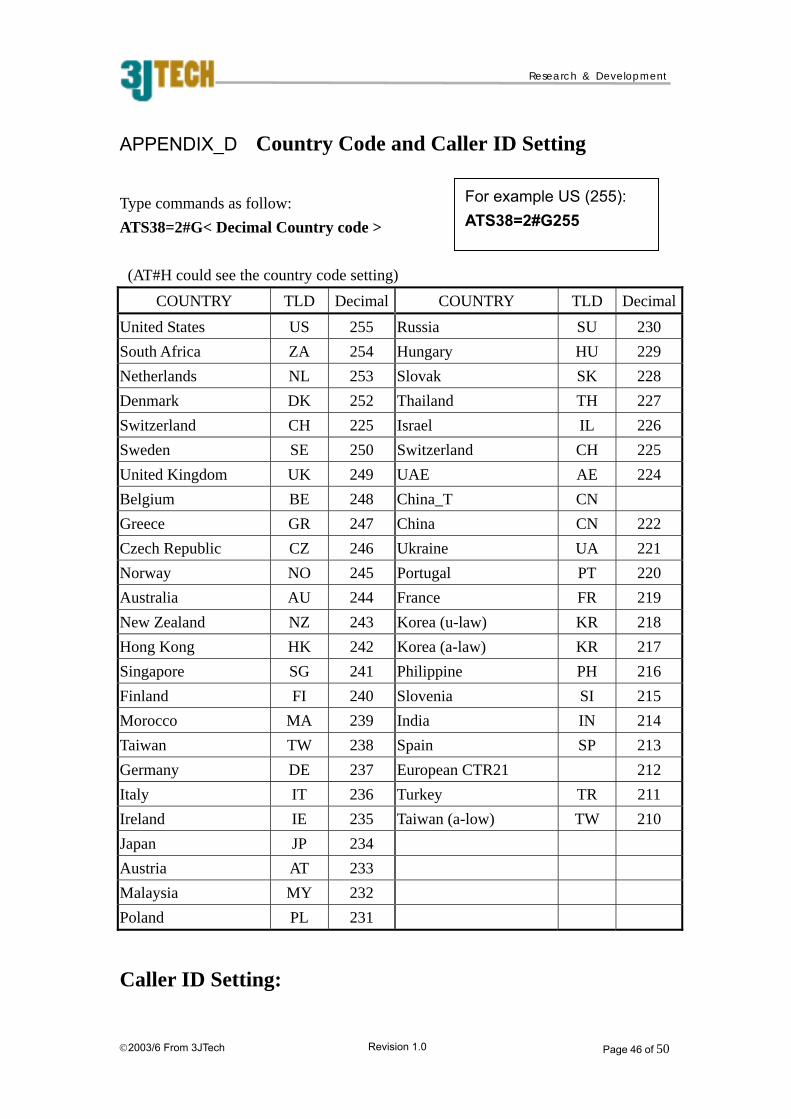
APPENDIX_D Country Code and Caller ID Setting
Type commands as follow: ATS38=2#G< Decimal Country code > (AT#H could see the country code setting)
COUNTRY TLD Decimal COUnited States US 255 Russia South Africa ZA 254 Hungary Netherlands NL 253 Slovak Denmark DK 252 Thailand Switzerland CH 225 Israel Sweden SE 250 SwitzerlaUnited Kingdom UK 249 UAE Belgium BE 248 China_T Greece GR 247 China Czech Republic CZ 246 Ukraine Norway NO 245 Portugal Australia AU 244 France New Zealand NZ 243 Korea (u-Hong Kong HK 242 Korea (a-Singapore SG 241 PhilippineFinland FI 240 Slovenia Morocco MA 239 India Taiwan TW 238 Spain Germany DE 237 EuropeanItaly IT 236 Turkey Ireland IE 235 Taiwan (aJapan JP 234 Austria AT 233 Malaysia MY 232 Poland PL 231
Caller ID Setting:
Revision 1.0 2003/6 From 3JTech
For example US (255):ATS38=2#G255
UNTRY TLD DecimalSU 230 HU 229 SK 228 TH 227 IL 226
nd CH 225 AE 224 CN CN 222 UA 221 PT 220 FR 219
law) KR 218 law) KR 217 PH 216
SI 215 IN 214 SP 213
CTR21 212 TR 211
-low) TW 210
Page 46 of 50

Research & Development
Enable Caller ID function (example for Taiwan): 1. Set country code to 238 (Taiwan). (“ATS38=2#G238“). 2. Set “ATS40.2=1” to enable CND function. The Caller ID function will be shown when detected. Use “AT*T” will show last caller ID message.
Page 47 of 50Revision 1.0 2003/6 From 3JTech

Research & Development
APPENDIX_E Firmware Upgrade
If you want to upgrade firmware online, you should make sure the modem chip is "ZD1051A" and the ROM is "Intel Flash TE28F800".
If uModem ROM code driver have been well installed, hyper terminal should have a new USB com port. Open this com port. Issue AT can get response then driver has been well installed.
Update procedure: a. For ZD1051A ROM code mode:
Issue “ATF”: select “4” for “Intel flash”. Issue “ATUPX”: select "Y". After "$" has appeared, use XModem to send file
(3JU*****.HEX) with kernel. b. At flash modem code mode: b.1 Update modem file only:
Issue “ATUPX”: select "Y". After "$" has appeared, use XModem to send file (3JU*****.FSH) without kernel.
b.2 Update modem with kernel changed:
Issue “ATBZYX”. Issue “ATUPXK”: select "Y". After "$" has appeared, use XModem to
send file (3JU*****.HEX) with kernel.
Page 48 of 50Revision 1.0 2003/6 From 3JTech
Research & Development
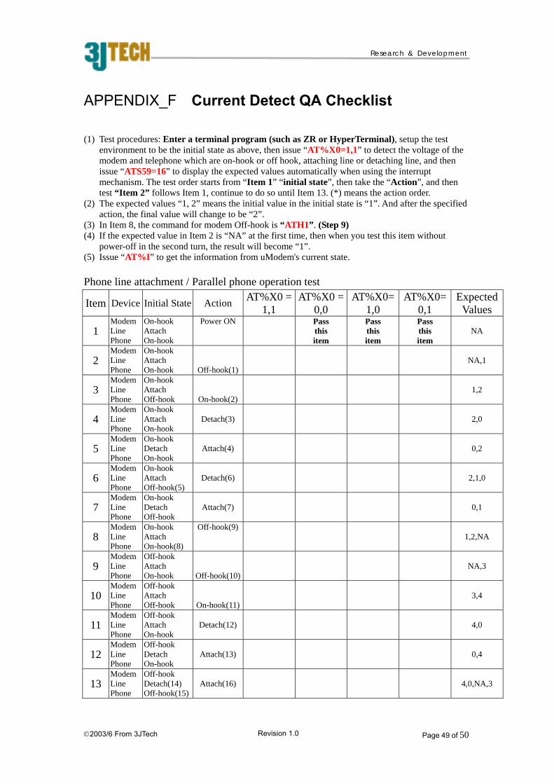
APPENDIX_F Current Detect QA Checklist
(1) Test procedures: Enter a terminal program (such as ZR or HyperTerminal), setup the test environment to be the initial state as above, then issue “AT%X0=1,1” to detect the voltage of the modem and telephone which are on-hook or off hook, attaching line or detaching line, and then issue “ATS59=16” to display the expected values automatically when using the interrupt mechanism. The test order starts from “Item 1” “initial state”, then take the “Action”, and then test “Item 2” follows Item 1, continue to do so until Item 13. (*) means the action order.
(2) The expected values “1, 2” means the initial value in the initial state is “1”. And after the specified action, the final value will change to be “2”.
(3) In Item 8, the command for modem Off-hook is “ATH1”. (Step 9) (4) If the expected value in Item 2 is “NA” at the first time, then when you test this item without
power-off in the second turn, the result will become “1”. (5) Issue “AT%I” to get the information from uModem's current state. Phone line attachment / Parallel phone operation test
Item Device Initial State Action AT%X0 =1,1
AT%X0 = 0,0
AT%X0= 1,0
AT%X0= 0,1
Expected Values
1 Modem Line Phone
On-hook Attach On-hook
Power ON Pass this item
Pass this item
Pass this item
NA
2 Modem Line Phone
On-hook Attach On-hook
Off-hook(1)
NA,1
3 Modem Line Phone
On-hook Attach Off-hook
On-hook(2)
1,2
4 Modem Line Phone
On-hook Attach On-hook
Detach(3)
2,0
5 Modem Line Phone
On-hook Detach On-hook
Attach(4)
0,2
6 Modem Line Phone
On-hook Attach Off-hook(5)
Detach(6)
2,1,0
7 Modem Line Phone
On-hook Detach Off-hook
Attach(7)
0,1
8 Modem Line Phone
On-hook Attach On-hook(8)
Off-hook(9) 1,2,NA
9 Modem Line Phone
Off-hook Attach On-hook
Off-hook(10)
NA,3
10 Modem Line Phone
Off-hook Attach Off-hook
On-hook(11)
3,4
11 Modem Line Phone
Off-hook Attach On-hook
Detach(12)
4,0
12 Modem Line Phone
Off-hook Detach On-hook
Attach(13)
0,4
13 Modem Line Phone
Off-hook Detach(14) Off-hook(15)
Attach(16)
4,0,NA,3
Page 49 of 50Revision 1.0 2003/6 From 3JTech
Research & Development
APPENDIX_G Advanced AT Commands (For Debug)
Command Function & Description ATREEP Display EEPROM ATREEP10000,256 Clear all EEPROM value to FF AT&T8 Modem send ASCII codes to PC continuous AT&T1 +++ AT#E1 AT#E0
Hardware noise testing
Page 50 of 50Revision 1.0 2003/6 From 3JTech