tcad technology cad process simulation dr. lynn … page 1 rochester institute of technology...
TRANSCRIPT

© March 10, 2008, Dr. Lynn Fuller, Professor
Rochester Institute of TechnologyMicroelectronic Engineering
TCAD
Page 1
ROCHESTER INSTITUTE OF TECHNOLOGYMICROELECTRONIC ENGINEERING
TCAD Technology CAD Process Simulation
Dr. Lynn Fuller Webpage: http://people.rit.edu/lffeee Microelectronic Engineering
Rochester Institute of Technology 82 Lomb Memorial Drive Rochester, NY 14623-5604 Tel (585) 475-2035 Fax (585) 475-5041
Email: [email protected] Department webpage: http://www.microe.rit.edu
3-10-2008 lec_tcad.ppt
© March 10, 2008, Dr. Lynn Fuller, Professor
Rochester Institute of TechnologyMicroelectronic Engineering
TCAD
Page 2
OUTLINE
IntroductionWhy SimulateProcess SimulationDevice SimulationCircuit SimulationHistorical Perspective of SimulatorsEvolution of the Complexity of Process SimulatorsOxidation SimulationImplant SimulationDiffusion Simulation2-d and 3-d SimulationSummaryReferencesHomework

© March 10, 2008, Dr. Lynn Fuller, Professor
Rochester Institute of TechnologyMicroelectronic Engineering
TCAD
Page 3
HIERARCHY OF SIMULATION TOOLS FOR IC DEVELOPMENT
© March 10, 2008, Dr. Lynn Fuller, Professor
Rochester Institute of TechnologyMicroelectronic Engineering
TCAD
Page 4
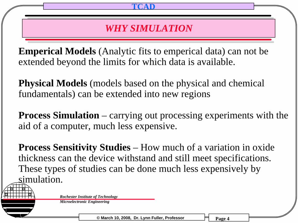
WHY SIMULATION
Emperical Models (Analytic fits to emperical data) can not be extended beyond the limits for which data is available.
Physical Models (models based on the physical and chemical fundamentals) can be extended into new regions
Process Simulation – carrying out processing experiments with the aid of a computer, much less expensive.
Process Sensitivity Studies – How much of a variation in oxide thickness can the device withstand and still meet specifications. These types of studies can be done much less expensively by simulation.

© March 10, 2008, Dr. Lynn Fuller, Professor
Rochester Institute of TechnologyMicroelectronic Engineering
TCAD
Page 5
PROCESS APPLICATIONS OF SIMULATION
Process Information Obtained by SimulationDoping profiles in silicon substrateDoping profiles in SiO2, Polysilicon and Silicide layersJunction depthsThickness of Material LayersTopographyLithography: resist profiles after developDevice cross-sections from layout

© March 10, 2008, Dr. Lynn Fuller, Professor
Rochester Institute of TechnologyMicroelectronic Engineering
TCAD
Page 6
PROCESS SIMULATION

© March 10, 2008, Dr. Lynn Fuller, Professor
Rochester Institute of TechnologyMicroelectronic Engineering
TCAD
Page 7
EXAMPLE DOPING PROFILES
1-D Doping Profile
2-D Doping Profile
© March 10, 2008, Dr. Lynn Fuller, Professor
Rochester Institute of TechnologyMicroelectronic Engineering
TCAD
Page 8
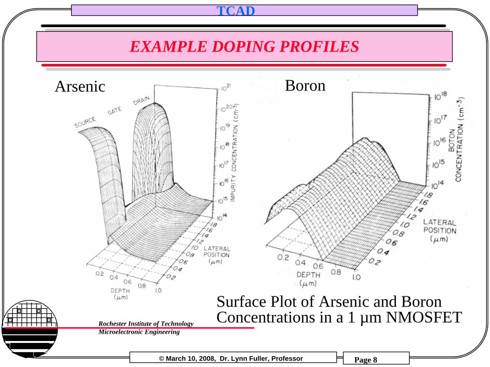
EXAMPLE DOPING PROFILES
Surface Plot of Arsenic and Boron Concentrations in a 1 µm NMOSFET
Arsenic Boron

© March 10, 2008, Dr. Lynn Fuller, Professor
Rochester Institute of TechnologyMicroelectronic Engineering
TCAD
Page 9
EXAMPLE DOPING PROFILES
Lateral Diffusion Of Impurities During FieldOxide Growth
BeforeOxidation
AfterOxidation

© March 10, 2008, Dr. Lynn Fuller, Professor
Rochester Institute of TechnologyMicroelectronic Engineering
TCAD
Page 10
DEPICT LITHOGRAPHY AND ETCH SIMULATOR
Resist Develop
Poly Etch
Oxide Etch
DEPICT

© March 10, 2008, Dr. Lynn Fuller, Professor
Rochester Institute of TechnologyMicroelectronic Engineering
TCAD
Page 11
DEVICE APPLICATIONS OF SIMULATION
Device Characteristics Obtained by SimulationPotential and Electric Field StrengthCarrier ConcentrationsSpace Charge RegionsCurrent Flow PathsFilm Sheet ResistanceThreshold VoltageSubthreshlod CurrentsDevice Isolation CharacteristicsLatch-up Effects in CMOSPunchthroughHot-carrier effects

© March 10, 2008, Dr. Lynn Fuller, Professor
Rochester Institute of TechnologyMicroelectronic Engineering
TCAD
Page 12
EXAMPLE OF BJT SIMULATION
CollectorCurrent
BaseCurrent
© March 10, 2008, Dr. Lynn Fuller, Professor
Rochester Institute of TechnologyMicroelectronic Engineering
TCAD
Page 13
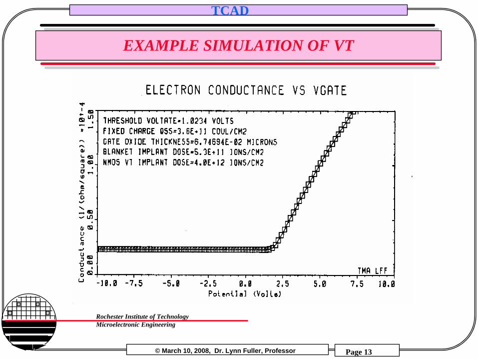
EXAMPLE SIMULATION OF VT

© March 10, 2008, Dr. Lynn Fuller, Professor
Rochester Institute of TechnologyMicroelectronic Engineering
TCAD
Page 14
EXAMPLE OF SIMULATION OF SPACE CHARGE REGION

© March 10, 2008, Dr. Lynn Fuller, Professor
Rochester Institute of TechnologyMicroelectronic Engineering
TCAD
Page 15
EXAMPLE DEVICE POTENTIAL AND ELECTRIC FIELD

© March 10, 2008, Dr. Lynn Fuller, Professor
Rochester Institute of TechnologyMicroelectronic Engineering
TCAD
Page 16
EXAMPLE OF SUB VT SLOPE SIMULATION
© March 10, 2008, Dr. Lynn Fuller, Professor
Rochester Institute of TechnologyMicroelectronic Engineering
TCAD
Page 17
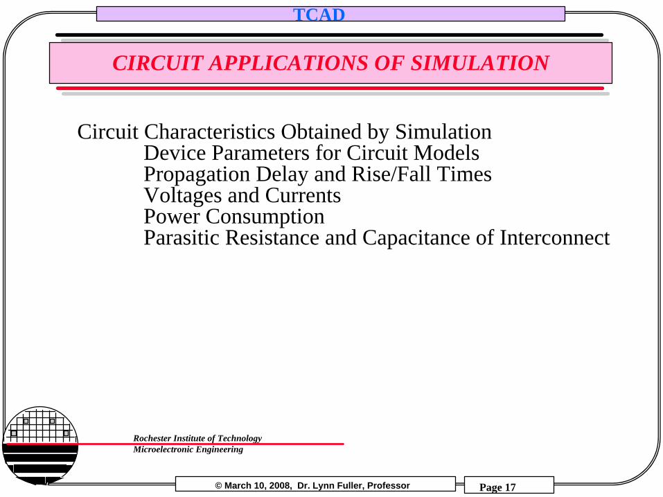
CIRCUIT APPLICATIONS OF SIMULATION
Circuit Characteristics Obtained by SimulationDevice Parameters for Circuit ModelsPropagation Delay and Rise/Fall TimesVoltages and CurrentsPower ConsumptionParasitic Resistance and Capacitance of Interconnect

© March 10, 2008, Dr. Lynn Fuller, Professor
Rochester Institute of TechnologyMicroelectronic Engineering
TCAD
Page 18
EXAMPLE OF CIRCUIT SIMULATION
Portout
Input A
XOR
Input BPort in
Port in
Vcc
Exclusive OR Circuit drawn by Jane Doe 10-3-97
XOR = A’B+AB’
A’
B
B’
A
A’B
AB’
00 0 0 0
0
0
00
0
1 1 1 1
1
1
1
0 100ns 200ns 300ns 400ns
/A input
/B input
/XORoutput
1 0
repeats
Verificationof the XOR circuit time
nanoseconds
Mentor GraphicsQuickSim (DigitalCircuit Simulation)

© March 10, 2008, Dr. Lynn Fuller, Professor
Rochester Institute of TechnologyMicroelectronic Engineering
TCAD
Page 19
EXAMPLE OF CIRCUIT SIMULATION
© March 10, 2008, Dr. Lynn Fuller, Professor
Rochester Institute of TechnologyMicroelectronic Engineering
TCAD
Page 20
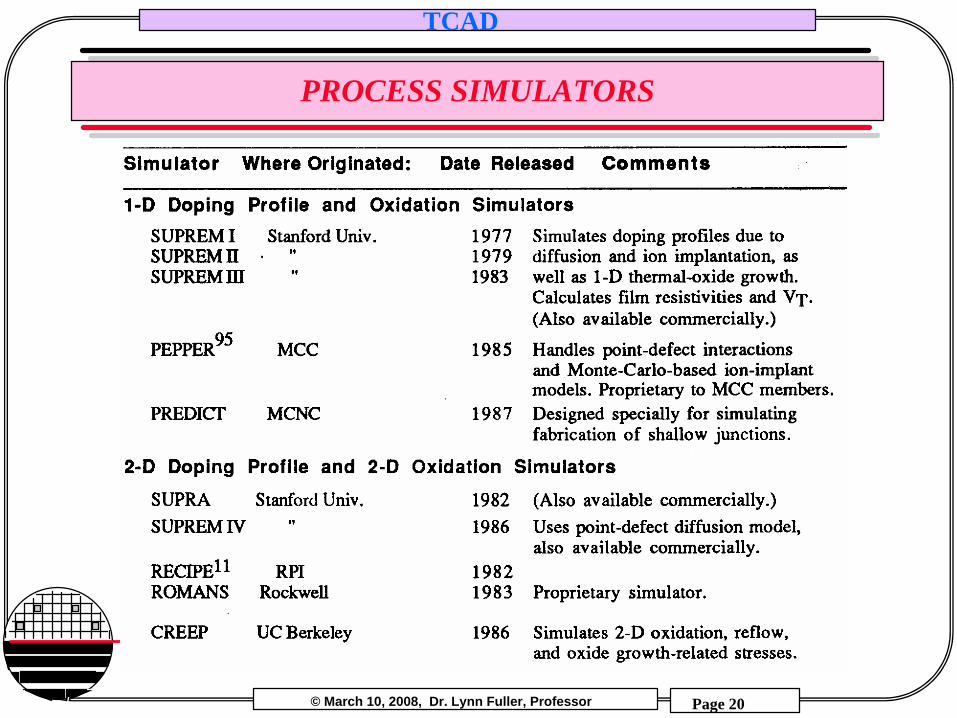
PROCESS SIMULATORS

© March 10, 2008, Dr. Lynn Fuller, Professor
Rochester Institute of TechnologyMicroelectronic Engineering
TCAD
Page 21
PROCESS SIMULATORS
© March 10, 2008, Dr. Lynn Fuller, Professor
Rochester Institute of TechnologyMicroelectronic Engineering
TCAD
Page 22
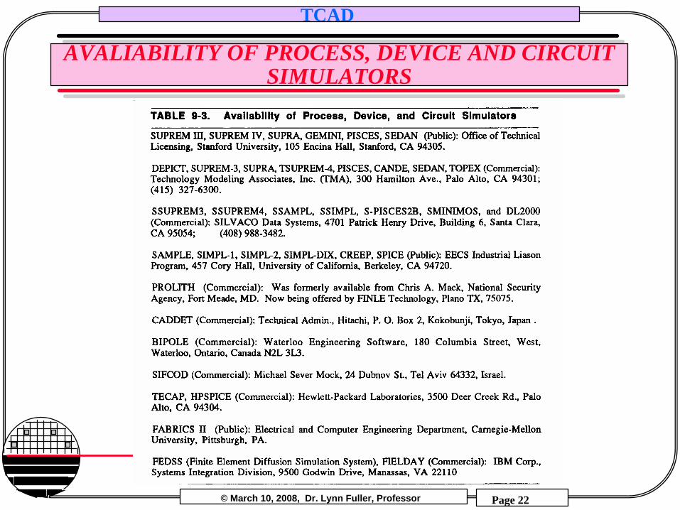
AVALIABILITY OF PROCESS, DEVICE AND CIRCUIT SIMULATORS
© March 10, 2008, Dr. Lynn Fuller, Professor
Rochester Institute of TechnologyMicroelectronic Engineering
TCAD
Page 23
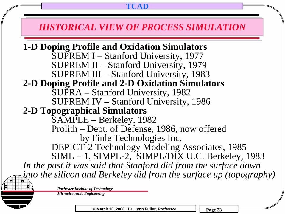
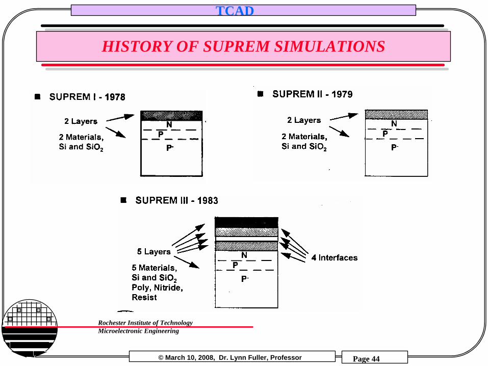
HISTORICAL VIEW OF PROCESS SIMULATION
1-D Doping Profile and Oxidation SimulatorsSUPREM I – Stanford University, 1977SUPREM II – Stanford University, 1979SUPREM III – Stanford University, 1983
2-D Doping Profile and 2-D Oxidation SimulatorsSUPRA – Stanford University, 1982SUPREM IV – Stanford University, 1986
2-D Topographical SimulatorsSAMPLE – Berkeley, 1982Prolith – Dept. of Defense, 1986, now offered
by Finle Technologies Inc.DEPICT-2 Technology Modeling Associates, 1985SIML – 1, SIMPL-2, SIMPL/DIX U.C. Berkeley, 1983
In the past it was said that Stanford did from the surface down into the silicon and Berkeley did from the surface up (topography)
© March 10, 2008, Dr. Lynn Fuller, Professor
Rochester Institute of TechnologyMicroelectronic Engineering
TCAD
Page 24
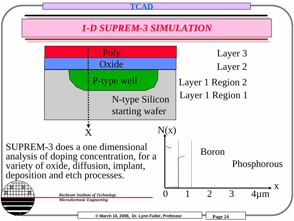
1-D SUPREM-3 SIMULATION
N-type Silicon starting wafer
P-type well
OxidePoly
Layer 2Layer 3
Layer 1 Region 2Layer 1 Region 1
X
x
N(x)
BoronPhosphorous
0 1 2 3 4µm
SUPREM-3 does a one dimensionalanalysis of doping concentration, for a variety of oxide, diffusion, implant, deposition and etch processes.

© March 10, 2008, Dr. Lynn Fuller, Professor
Rochester Institute of TechnologyMicroelectronic Engineering
TCAD
Page 25
SUPREM-3 INPUT FILE DETAILS
1… TITLE SIMULATION FOR NMOS TRANSISTOR IN THE PWELL3… Com Date: 5/3/994… Com edited by L.Fuller for EMCR 7325… Com Location pwellcmos1.in 635dept emcr650.suprem6… Com7… Initialize silicon (100) P=7E14 thickness=8 dx=0.028… Com9… Com Ramp Rate is taken as 16 C/min up and –8 C/min down10… Com All furnace steps push at 12 in/min at 900 C then11… Com Ramp up to soak temp ant then soak for the given time followed12… Com by ramp down to 1000 C and pull at 12 in/min13… Com Step1 ID01 Scribe Wafers14… Com Step2 DE01 Four Point Probe15… Com Step3 CL01 RCA Cleaned16… Com Step4 Alignment Oxide Growth18… Diffusion Time=12.5 Temp=900 WetO2 T.Rate=1219… Diffusion Time=35 Temp=1100 WetO220… Diffusion Time=12.5 Temp=1100 WetO2 T.Rate=-8
© March 10, 2008, Dr. Lynn Fuller, Professor
Rochester Institute of TechnologyMicroelectronic Engineering
TCAD
Page 26
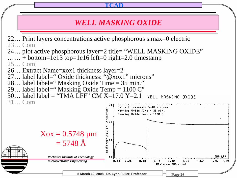
WELL MASKING OXIDE
22… Print layers concentrations active phosphorous s.max=0 electric23… Com24… plot active phosphorous layer=2 title= “WELL MASKING OXIDE”…… + bottom=1e13 top=1e16 left=0 right=2.0 timestamp25… Com26… Extract Name=xox1 thickness layer=227… label label=“ Oxide thickness: “@xox1” microns”28… label label=“ Masking Oxide Time = 35 min.”29… label label=“ Masking Oxide Temp = 1100 C”30… label label = “TMA LFF” CM X=17.0 Y=2.131… Com
Xox = 0.5748 µm= 5748 Å

© March 10, 2008, Dr. Lynn Fuller, Professor
Rochester Institute of TechnologyMicroelectronic Engineering
TCAD
Page 27
WELL IMPLANT AND DRIVE
32… Com Step5 Ph03 Photo level 1 Well Region33… Com Step6 ET06 Oxide Etch34… Etch Oxide35… Com Step7 IM01 Implant Well36… Assign name=dwell n.value=4E1237… Assign name=ewell N.value=5038… Implant Boron Dose = dwell Energy = ewell39… Com Step 8 ET07 Strip photoresist40… Com Step9 Cl01 RCA Clean41… Com Step10 OX06 Well Drive41… Diffusion Temperature = 900 t.Final = 1125 Dryo2 Time=1442… Diffusion Time=240 Temperature= 1125 Dryo243… Diffusion Time=960 Temperature=1125 Nitrogen45… Diffusion Temperature=1125 T.Final=1000 Nitrogen Time=15.646… print layers concentrations_active_phosphorous boron combine layer=1
+ x.max=0 electric48… Extract Name=xox3 thickness layer=249… Extract Name=xjw net active x.extract y=050… Electrical steps = 151… Bias layer=1 V=052… End53… Extract Name=Rsw h.resistance layer=1 min.region=255… Plot net active title=“IMPURITY PROFILE AFTER WELL DRIVE”
… +

© March 10, 2008, Dr. Lynn Fuller, Professor
Rochester Institute of TechnologyMicroelectronic Engineering
TCAD
Page 28
AFTER WELL DRIVE
© March 10, 2008, Dr. Lynn Fuller, Professor
Rochester Institute of TechnologyMicroelectronic Engineering
TCAD
Page 29
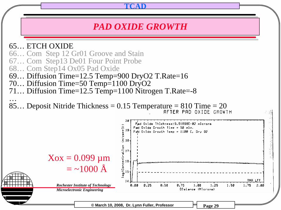
PAD OXIDE GROWTH
65… ETCH OXIDE66… Com Step 12 Gr01 Groove and Stain67… Com Step13 De01 Four Point Probe68… Com Step14 Ox05 Pad Oxide69… Diffusion Time=12.5 Temp=900 DryO2 T.Rate=1670… Diffusion Time=50 Temp=1100 DryO271… Diffusion Time=12.5 Temp=1100 Nitrogen T.Rate=-8…85… Deposit Nitride Thickness = 0.15 Temperature = 810 Time = 20
Xox = 0.099 µm= ~1000 Å

© March 10, 2008, Dr. Lynn Fuller, Professor
Rochester Institute of TechnologyMicroelectronic Engineering
TCAD
Page 30
AFTER FIELD OXIDE GROWTH
Xox = ~ 1000 ÅBecause nitride protects area over the well
97… Com Step24 Ox05 Field Oxide98… Diffusion Time=12.5 Temp=900 WetO2 T.Rate=1699… Diffusion Time=210 Temp=1100 WetO2100… Diffusion Time=12.5 Temp=1100 Nitrogen T.Rate=-8…115… Etch Oxide116… Etch Nitride117… Etch Oxide

© March 10, 2008, Dr. Lynn Fuller, Professor
Rochester Institute of TechnologyMicroelectronic Engineering
TCAD
Page 31
KOOI OXIDE GROWTH
120… Com Step29 Ox04 Kooi Oxide Growth121… Diffusion Time=45 Temp=900 WetO2

© March 10, 2008, Dr. Lynn Fuller, Professor
Rochester Institute of TechnologyMicroelectronic Engineering
TCAD
Page 32
NMOS THRESHOLD ADJUST IMPLANT & ANNEAL
135… Com Step30 Im01 PMOS Vt Adjust Ion Implant (blanket Implant)136… Assign Name=DPVT N.Value=5.3E11137… Assign Name=EPVT N.Value=60138… Implant Boron Dose= DPVT Energy=EPVT139… Com Step31 Ph03 Photo Level 4 NMOS Vt Adjust140… Com Step32 Im01 NMOS VT Adjust Ion Implant (masked Implant)141… Assign Name=DNVT N.Value=4E12142… Assign Name=ENVT N.Value=60138… Implant Boron Dose= DNVT Energy=ENVT
© March 10, 2008, Dr. Lynn Fuller, Professor
Rochester Institute of TechnologyMicroelectronic Engineering
TCAD
Page 33
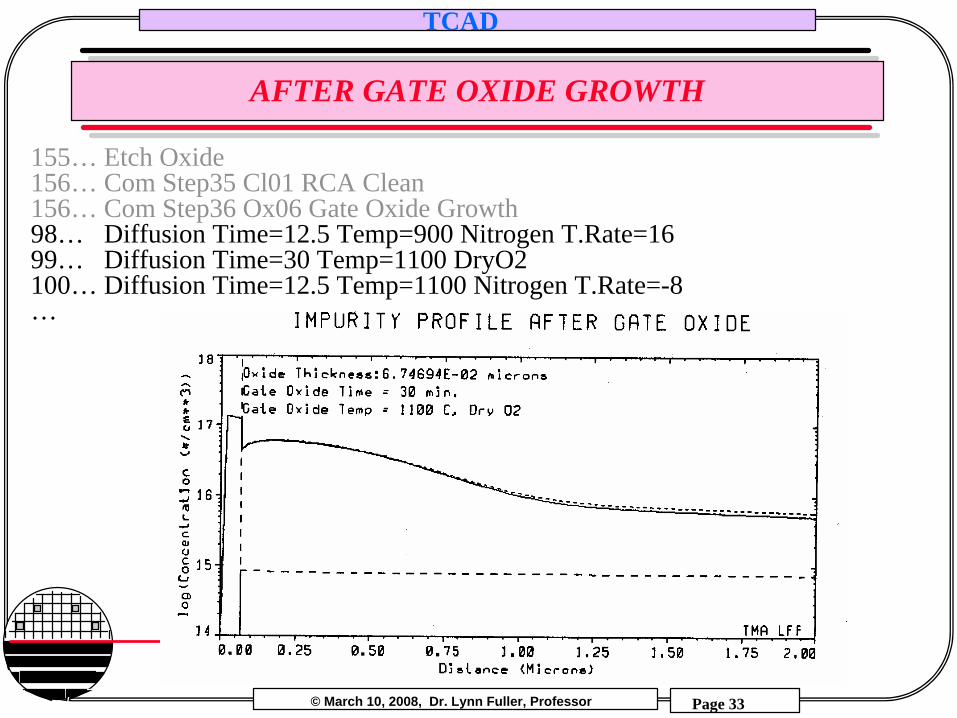
AFTER GATE OXIDE GROWTH
155… Etch Oxide156… Com Step35 Cl01 RCA Clean156… Com Step36 Ox06 Gate Oxide Growth98… Diffusion Time=12.5 Temp=900 Nitrogen T.Rate=1699… Diffusion Time=30 Temp=1100 DryO2100… Diffusion Time=12.5 Temp=1100 Nitrogen T.Rate=-8…
© March 10, 2008, Dr. Lynn Fuller, Professor
Rochester Institute of TechnologyMicroelectronic Engineering
TCAD
Page 34
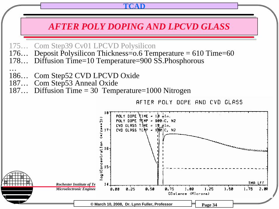
AFTER POLY DOPING AND LPCVD GLASS
175… Com Step39 Cv01 LPCVD Polysilicon176… Deposit Polysilicon Thickness=o.6 Temperature = 610 Time=60178… Diffusion Time=10 Temperature=900 SS.Phosphorous…186… Com Step52 CVD LPCVD Oxide187… Com Step53 Anneal Oxide187… Diffusion Time = 30 Temperature=1000 Nitrogen
© March 10, 2008, Dr. Lynn Fuller, Professor
Rochester Institute of TechnologyMicroelectronic Engineering
TCAD
Page 35
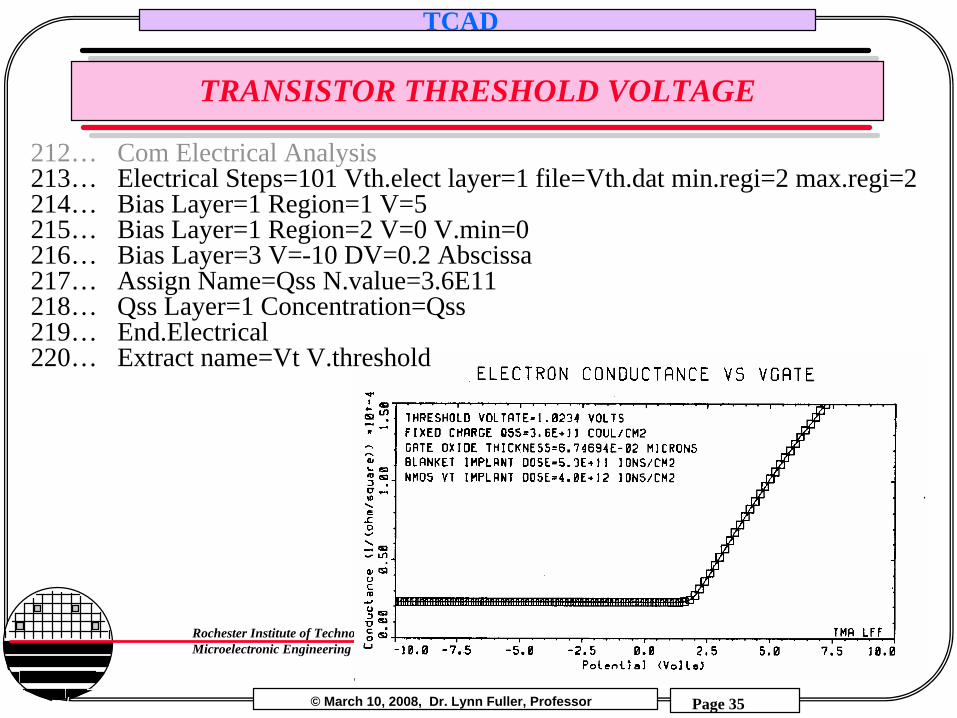
TRANSISTOR THRESHOLD VOLTAGE
212… Com Electrical Analysis213… Electrical Steps=101 Vth.elect layer=1 file=Vth.dat min.regi=2 max.regi=2214… Bias Layer=1 Region=1 V=5215… Bias Layer=1 Region=2 V=0 V.min=0216… Bias Layer=3 V=-10 DV=0.2 Abscissa217… Assign Name=Qss N.value=3.6E11218… Qss Layer=1 Concentration=Qss219… End.Electrical220… Extract name=Vt V.threshold
© March 10, 2008, Dr. Lynn Fuller, Professor
Rochester Institute of TechnologyMicroelectronic Engineering
TCAD
Page 36
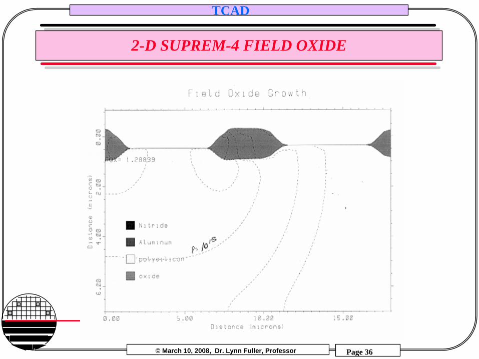
2-D SUPREM-4 FIELD OXIDE

© March 10, 2008, Dr. Lynn Fuller, Professor
Rochester Institute of TechnologyMicroelectronic Engineering
TCAD
Page 37
2-D SUPREM-4 P-WELL CMOS

© March 10, 2008, Dr. Lynn Fuller, Professor
Rochester Institute of TechnologyMicroelectronic Engineering
TCAD
Page 38
2-D SUPREM-4 CHANNEL STOP IMPLANT
© March 10, 2008, Dr. Lynn Fuller, Professor
Rochester Institute of TechnologyMicroelectronic Engineering
TCAD
Page 39
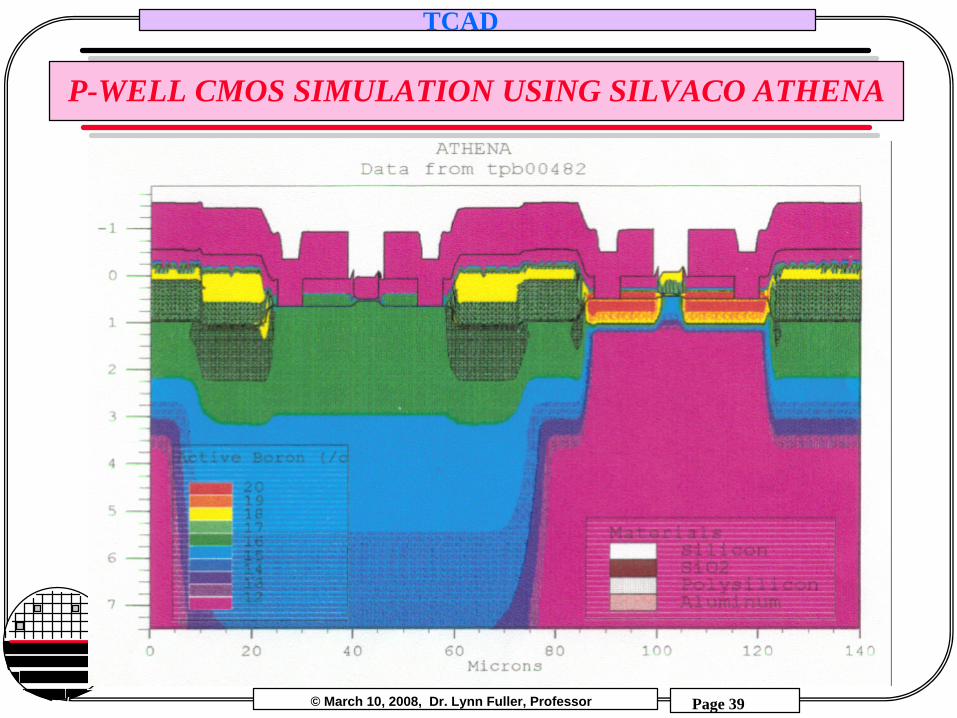
P-WELL CMOS SIMULATION USING SILVACO ATHENA

© March 10, 2008, Dr. Lynn Fuller, Professor
Rochester Institute of TechnologyMicroelectronic Engineering
TCAD
Page 40
2-D SUPREM-4 ANALYSIS OF BIRDS BEAK

© March 10, 2008, Dr. Lynn Fuller, Professor
Rochester Institute of TechnologyMicroelectronic Engineering
TCAD
Page 41
DEFECTS CAUSED BY STRESS IN LOCOS PROCESS
The stress can be large enough to cause damage in the silicon at the edge of the LOCOS. The D/S junctions are also located at the edge of the LOCOS. The result is that the junctions are leaky.
Stress increases with increased nitride thickness, increased field oxide thickness and decreased pad oxide thickness. In the RIT Pwell CMOS process pad oxide is 500 Å, nitride is 1500 Å and field oxide is 11,000 Å. We may get more reliable results by decreasing the nitride to 1000 Å and decreasing the field oxide to 8000 Å

© March 10, 2008, Dr. Lynn Fuller, Professor
Rochester Institute of TechnologyMicroelectronic Engineering
TCAD
Page 42
HISTORY OF SILICON OXIDE SIMULATION
All oxide simulations are based on the work of Deal and Grove done in the early 1960’s

© March 10, 2008, Dr. Lynn Fuller, Professor
Rochester Institute of TechnologyMicroelectronic Engineering
TCAD
Page 43
HISTORY OF SILICON OXIDE SIMULATION
© March 10, 2008, Dr. Lynn Fuller, Professor
Rochester Institute of TechnologyMicroelectronic Engineering
TCAD
Page 44
HISTORY OF SUPREM SIMULATIONS

© March 10, 2008, Dr. Lynn Fuller, Professor
Rochester Institute of TechnologyMicroelectronic Engineering
TCAD
Page 45
SYSTEM OF EQUATIONS TO BE SOLVED

© March 10, 2008, Dr. Lynn Fuller, Professor
Rochester Institute of TechnologyMicroelectronic Engineering
TCAD
Page 46
SUMMARY
SUPREM analysis allows for the calculation of resultant impurityconcentrations for processes such as oxidation, diffusion, implantation and deposition for temperatures above 800 C.

© March 10, 2008, Dr. Lynn Fuller, Professor
Rochester Institute of TechnologyMicroelectronic Engineering
TCAD
Page 47
REFERENCES
1. Silicon Processing for the VLSI Era, Vol.2., Stanly Wolf, 1990.2. The Science and Engineering of Microelectronic Processing,
Stephen Campbell.3. Technology Modeling Associates, TMA-SUPREM-4, Instruction
Manual.4. Silvaco Modeling, Inc.5. MicroTec-3.03 release note of March 27, 1998 floppy-disk
contains a complete set of MicroTec-3.03 programs for 2D semiconductor process and device simulation and the Manual in Adobe Acrobat format. http://www.siborg.ca
6. Silicon Processing for the VLSI Era, Vol.3., Ch.9., StanlyWolf7. VLSI Technology, 2nd Ed. By S.M.Sze, McGraw Hill, Ch.10.,
1988.
© March 10, 2008, Dr. Lynn Fuller, Professor
Rochester Institute of TechnologyMicroelectronic Engineering
TCAD
Page 48
HOMEWORK - TCAD
1.