taiwan is silicon island - oc oerlikon industry sourcebook 1999 progress of flip chip technology...
TRANSCRIPT
Semiconductor Industry Sourcebook1999
Progress of Flip Chip Technology
Taiwan is Silicon Island
Metallization, FRAMs, MRAMs
All about SiGe Technology
High-performance Failure Analysis
Progress of Flip Chip Technology
Taiwan is Silicon Island
Metallization, FRAMs, MRAMs
All about SiGe Technology
High-performance Failure Analysis

Since the fourth quarter of 1998
forecasts for 1999 have slowly but surely
been readjusted upwards. What was once
termed as a year of damage control now
looks a bit more sympathetic. Dataquest
predicts modest overall growth of 5-10%
for the industry (see chart) and other
industry analysts are now quoting
increases of up to 18%. Both numbers are
a sizeable improvement over the past three
downturn years, including last year’s
decrease of 8.4% in business.
is expected to shrink by 1-2% during this
year - after a 23.3% decrease in 1998 and
over $35 billion in new fab cancellations
in the last 18 months. The equipment
market will remain slow until the fourth
quarter, when many industry analysts
forecast a noticeable upturn in orders.
BPS on track
Despite differing reports, for the
market segments serviced by BPS, the
Asia-Pacific region will show clear gains
this year. Taiwan’s rate of investment has
held up during the financial crisis, but
overall spending will decrease during
1999. Korea may be the surprise turn-
around, as we have already booked new
equipment orders there and look for
perhaps a 20% jump in growth! Japan
shows no major spending rate changes for
this year, with liquidity and local
economic issues dominating the country’s
industry. Europe also shows signs of
consistent growth for the year, a good sign
for BPS. Our markets in North America
were strong in 1998 and overall
investment spending for 1999 started slow
but prospects for the rest of the year look
excellent.
Fortunately, last year’s overall market
trends were not reflected by the results at
BPS. Across all our segments – packaging,
front end, telecom, and failure analysis –
we managed to increase business volume
by 25% over the whole year. Our current
programs maintain a strong R&D focus to
help us hold profitability levels and
strengthen our market positions. All our
new equipment and process development
programs for 1999 are set to launch on
time.
SiGe and other new members
There is usually a “technology-bias” to
equipment orders that precede the volume
orders signaling an industry-wide recovery.
Right now, we have a lot of customer
interest in our new production
technologies and are set to introduce
numerous innovations in 1999.
Another reason for an optimistic
future at BPS is the integration of the new
silicon-germanium activities, formerly at
BP
S t
od
ay
...
BP
S t
od
ay
...
BP
S t
od
ay
...
BP
S t
od
ay
...
BP
S t
od
ay
...
BP
S t
od
ay
...
BP
S t
od
ay
...
Chip
Semiconductor Industry Sourcebook
3
Small Steps LEAD TO
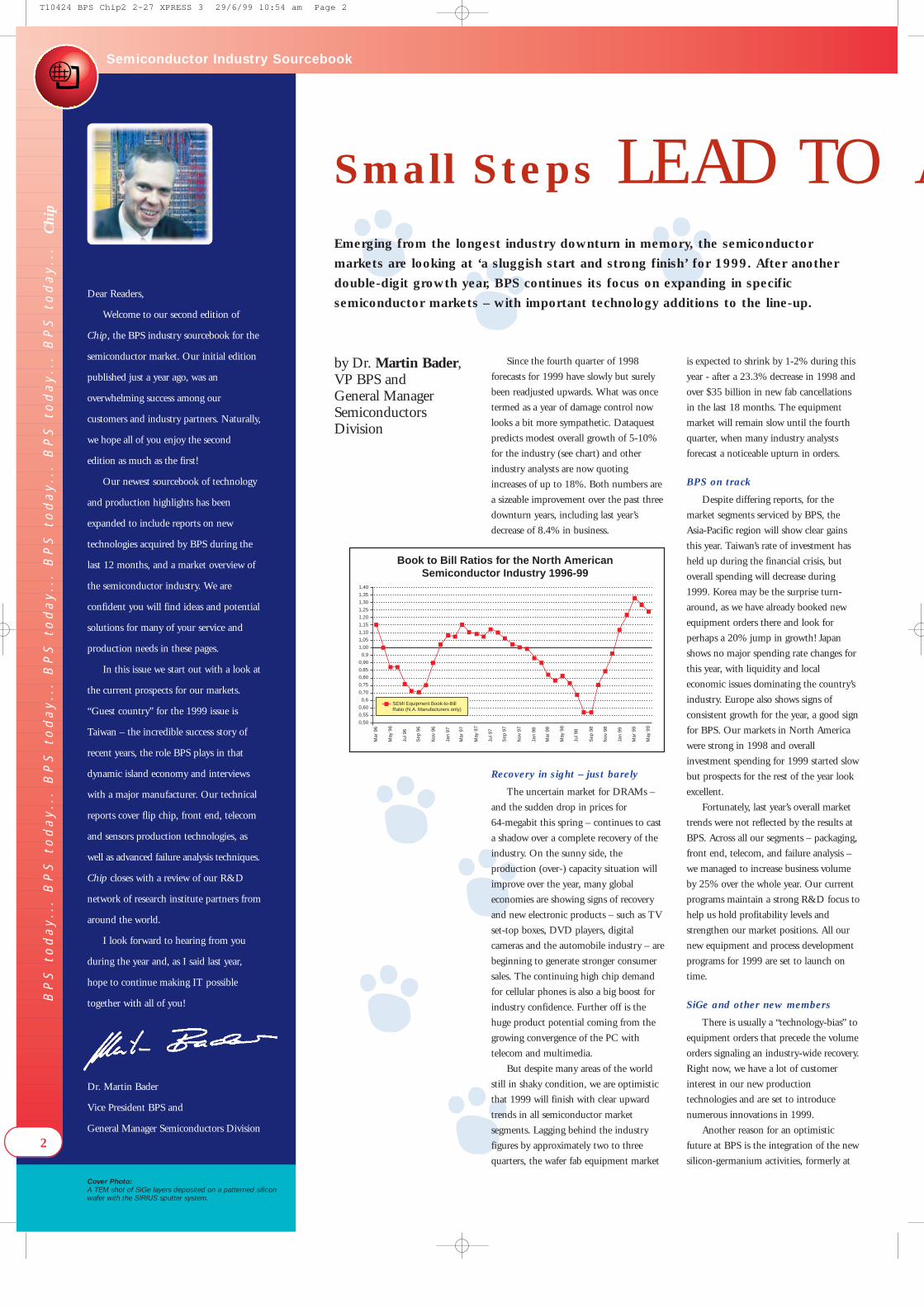
by Dr. Martin Bader,VP BPS and General ManagerSemiconductorsDivision
Emerging from the longest industry downturn in memory, the semiconductor
markets are looking at ‘a sluggish start and strong finish’ for 1999. After another
double-digit growth year, BPS continues its focus on expanding in specific
semiconductor markets – with important technology additions to the line-up.Dear Readers,
Welcome to our second edition of
Chip, the BPS industry sourcebook for the
semiconductor market. Our initial edition
published just a year ago, was an
overwhelming success among our
customers and industry partners. Naturally,
we hope all of you enjoy the second
edition as much as the first!
Our newest sourcebook of technology
and production highlights has been
expanded to include reports on new
technologies acquired by BPS during the
last 12 months, and a market overview of
the semiconductor industry. We are
confident you will find ideas and potential
solutions for many of your service and
production needs in these pages.
In this issue we start out with a look at
the current prospects for our markets.
“Guest country” for the 1999 issue is
Taiwan – the incredible success story of
recent years, the role BPS plays in that
dynamic island economy and interviews
with a major manufacturer. Our technical
reports cover flip chip, front end, telecom
and sensors production technologies, as
well as advanced failure analysis techniques.
Chip closes with a review of our R&D
network of research institute partners from
around the world.
I look forward to hearing from you
during the year and, as I said last year,
hope to continue making IT possible
together with all of you!
Dr. Martin Bader
Vice President BPS and
General Manager Semiconductors Division
Mar
96
1,40
1,35
1,30
1,25
1,20
1,15
1,10
1,05
1,00
0,9
0,90
0,85
0,80
0,75
0,70
0,6
0,60
0,55
0,50
May
96
Jul 9
6
Sep
96
Nov
96
Jan
97
Mar
97
May
97
Jul 9
7
Sep
97
Nov
97
Jan
98
Mar
98
May
98
Jul 9
8
Sep
98
Nov
98
Jan
99
Mar
99
May
99
SEMI Equipment Book-to-BillRatio (N.A. Manufacturers only)
Book to Bill Ratios for the North AmericanSemiconductor Industry 1996-99
Recovery in sight – just barely
The uncertain market for DRAMs –
and the sudden drop in prices for
64-megabit this spring – continues to cast
a shadow over a complete recovery of the
industry. On the sunny side, the
production (over-) capacity situation will
improve over the year, many global
economies are showing signs of recovery
and new electronic products – such as TV
set-top boxes, DVD players, digital
cameras and the automobile industry – are
beginning to generate stronger consumer
sales. The continuing high chip demand
for cellular phones is also a big boost for
industry confidence. Further off is the
huge product potential coming from the
growing convergence of the PC with
telecom and multimedia.
But despite many areas of the world
still in shaky condition, we are optimistic
that 1999 will finish with clear upward
trends in all semiconductor market
segments. Lagging behind the industry
figures by approximately two to three
quarters, the wafer fab equipment market
Cover Photo:A TEM shot of SiGe layers deposited on a patterned siliconwafer with the SIRIUS sputter system.
Since the fourth quarter of 1998
forecasts for 1999 have slowly but surely
been readjusted upwards. What was once
termed as a year of damage control now
looks a bit more sympathetic. Dataquest
predicts modest overall growth of 5-10%
for the industry (see chart) and other
industry analysts are now quoting
increases of up to 18%. Both numbers are
a sizeable improvement over the past three
downturn years, including last year’s
decrease of 8.4% in business.
is expected to shrink by 1-2% during this
year - after a 23.3% decrease in 1998 and
over $35 billion in new fab cancellations
in the last 18 months. The equipment
market will remain slow until the fourth
quarter, when many industry analysts
forecast a noticeable upturn in orders.
BPS on track
Despite differing reports, for the
market segments serviced by BPS, the
Asia-Pacific region will show clear gains
this year. Taiwan’s rate of investment has
held up during the financial crisis, but
overall spending will decrease during
1999. Korea may be the surprise turn-
around, as we have already booked new
equipment orders there and look for
perhaps a 20% jump in growth! Japan
shows no major spending rate changes for
this year, with liquidity and local
economic issues dominating the country’s
industry. Europe also shows signs of
consistent growth for the year, a good sign
for BPS. Our markets in North America
were strong in 1998 and overall
investment spending for 1999 started slow
but prospects for the rest of the year look
excellent.
Fortunately, last year’s overall market
trends were not reflected by the results at
BPS. Across all our segments – packaging,
front end, telecom, and failure analysis –
we managed to increase business volume
by 25% over the whole year. Our current
programs maintain a strong R&D focus to
help us hold profitability levels and
strengthen our market positions. All our
new equipment and process development
programs for 1999 are set to launch on
time.
SiGe and other new members
There is usually a “technology-bias” to
equipment orders that precede the volume
orders signaling an industry-wide recovery.
Right now, we have a lot of customer
interest in our new production
technologies and are set to introduce
numerous innovations in 1999.
Another reason for an optimistic
future at BPS is the integration of the new
silicon-germanium activities, formerly at
BP
S t
od
ay
...
BP
S t
od
ay
...
BP
S t
od
ay
...
BP
S t
od
ay
...
BP
S t
od
ay
...
BP
S t
od
ay
...
BP
S t
od
ay
...
Chip
Semiconductor Industry Sourcebook
2
Small Steps LEAD TO A
by Dr. Martin Bader,VP BPS and General ManagerSemiconductorsDivision
Emerging from the longest industry downturn in memory, the semiconductor
markets are looking at ‘a sluggish start and strong finish’ for 1999. After another
double-digit growth year, BPS continues its focus on expanding in specific
semiconductor markets – with important technology additions to the line-up.Dear Readers,
Welcome to our second edition of
Chip, the BPS industry sourcebook for the
semiconductor market. Our initial edition
published just a year ago, was an
overwhelming success among our
customers and industry partners. Naturally,
we hope all of you enjoy the second
edition as much as the first!
Our newest sourcebook of technology
and production highlights has been
expanded to include reports on new
technologies acquired by BPS during the
last 12 months, and a market overview of
the semiconductor industry. We are
confident you will find ideas and potential
solutions for many of your service and
production needs in these pages.
In this issue we start out with a look at
the current prospects for our markets.
“Guest country” for the 1999 issue is
Taiwan – the incredible success story of
recent years, the role BPS plays in that
dynamic island economy and interviews
with a major manufacturer. Our technical
reports cover flip chip, front end, telecom
and sensors production technologies, as
well as advanced failure analysis techniques.
Chip closes with a review of our R&D
network of research institute partners from
around the world.
I look forward to hearing from you
during the year and, as I said last year,
hope to continue making IT possible
together with all of you!
Dr. Martin Bader
Vice President BPS and
General Manager Semiconductors Division
Mar
96
1,40
1,35
1,30
1,25
1,20
1,15
1,10
1,05
1,00
0,9
0,90
0,85
0,80
0,75
0,70
0,6
0,60
0,55
0,50
May
96
Jul 9
6
Sep
96
Nov
96
Jan
97
Mar
97
May
97
Jul 9
7
Sep
97
Nov
97
Jan
98
Mar
98
May
98
Jul 9
8
Sep
98
Nov
98
Jan
99
Mar
99
May
99
SEMI Equipment Book-to-BillRatio (N.A. Manufacturers only)
Book to Bill Ratios for the North AmericanSemiconductor Industry 1996-99
Recovery in sight – just barely
The uncertain market for DRAMs –
and the sudden drop in prices for
64-megabit this spring – continues to cast
a shadow over a complete recovery of the
industry. On the sunny side, the
production (over-) capacity situation will
improve over the year, many global
economies are showing signs of recovery
and new electronic products – such as TV
set-top boxes, DVD players, digital
cameras and the automobile industry – are
beginning to generate stronger consumer
sales. The continuing high chip demand
for cellular phones is also a big boost for
industry confidence. Further off is the
huge product potential coming from the
growing convergence of the PC with
telecom and multimedia.
But despite many areas of the world
still in shaky condition, we are optimistic
that 1999 will finish with clear upward
trends in all semiconductor market
segments. Lagging behind the industry
figures by approximately two to three
quarters, the wafer fab equipment market
Cover Photo:A TEM shot of SiGe layers deposited on a patterned siliconwafer with the SIRIUS sputter system.
T10424 BPS Chip2 2-27 XPRESS 3 29/6/99 10:54 am Page 2

Leybold Systems. This move unites all
semiconductor production applications
under BPS. This technology transfer
includes the SiGe development team,
established industry partnership programs
and the proven SIRIUS tool (see our
detailed report on page 30). Further
projects in the telecom and packaging
market segments round out our new
product developments.
Cluster tool as a bridge tool
The ongoing optimization of new
processes and hardware for our cluster tool
platform continues to bear fruit: after the
launch of an RTP process module, we
have just announced a dedicated tooling
set for thin wafer processing; both for
150 mm and 200mm applications. The
ongoing expansion and optimization of
applications for the cluster tool is one of
BPS’ major priorities, which points to
continuing development efforts for our
300mm system.
In the question of “300mm or not”,
current economic conditions have
postponed the introduction of 300mm
projects by at least one year. While the
biggest and costliest investment effort in
the history of the industry lags, 8-10 pilot
production lines are forecast to be on-line
by 2001. Until then, the larger cluster tool
platforms can be used for continued R&D
with 200mm wafers.
Our offer is a bridge tool option that
easily adapts the 300mm cluster tool to
the smaller 200mm format. This option
simplifies ramp-up to 300mm wafers by
simply exchanging the tooling kit and
minimizes the risk involved with a switch
to a larger wafer format.
Editor in Chief: Dr. Martin Bader
Managing Editor: Juerg Steinmann
Editorial: Peter Kraus, REMCOM
Design/Layout: OTM Design, London
Published by: Balzers Process Systems, P.O. Box 1000, 9496 Balzers, Liechtenstein
Photography: Alberto Venzago
Printed in England on recycled paper.
Please feel free to contact us:Fax: +423 388 6539E-mail: [email protected]
Chip – the Semiconductor Sourcebook is also available onlineat our Web site
Chip editorial 2
Small Steps Lead to a Better Future 2
BPS around the semiconductor globe 4
Silicon Island 6
Growing with our Customers 8
Thinking Locally, Acting Globally 9
Chip Packagers 10
Progress in Flip Chip Packaging Technology 12
Volume Production Solutions for UBM 14
Flip Chip Matrix 17
Moving Up with Backside Metallization 18
Software Issues with Cluster Tools forIC Manufacturing 19
Multi-Level Metallization for IC Inter Connects 20
A Stand-Alone Solution for RTP 21
MRAM – A New Memory Technologyon the Horizon 22
The Complexity of Manufacturing FRAMS 23
Front End Matrix 25
The Breakthrough for SiGe Was Yesterday! 26
The Promise of SiGe: Technologyand Markets 28
A Proven UHV-CVD Solution for SiGe 30
Using LEPECVD for SiGe 32
Enhanced SAW Processing 34
SAWs Made in Europe 35
Staying Up-To-Date on Bulk AcousticWave Devices 36
Improving InP Reactive Ion Etching 38
Telecoms and Sensors Matrix 39
HIgh Performance Tool for FailureAnalysis 40
The Pearl of Failure Analysis 42
Failure and Low Yield Analysis Matrix 43
High-Tech Source in the Rhine Valley 44
TThe Institute for Reliability and Microintegration at the Fraunhofer Institute in Berlin 46
The Silicon Heterostructures Group at theFederal Institute of Technology in Zürich 46
The Ceramic Laboratory at the Federal Institute of Technology in Lausanne 47
The Microelectronics Centre at theNanyang Technological University in Singapore 47
www.bps -IT.com
BP
S t
od
ay
...
BP
S t
od
ay
...
BP
S t
od
ay
...
BP
S t
od
ay
...
BP
S t
od
ay
...
BP
S t
od
ay
...
BP
S t
od
ay
...
Chip
Semiconductor Industry Sourcebook
3
29%
24%27%
5%3%
26%
46%
-17%
24% 24%
39%
7%
2%
8%10%
29%32%
42%
-9%
4%
-8%
11%
23%
31%
Annual sales neverget close to averageindustry growth rate
Average chipindustry growthrate is 15%
Source: IC Insights, WSTS
78
29% change
79 80 81 82 83 84 85 86 87 88 89 90 91 92 93 94 95 96 97 98 99F 00F 01F
24 27 5 3 26 46 -17 24 24 39 7 2 8 10 29 32 42 -9 4 -8 11 23 31
Global Semiconductor Industry Growth Rate 1978-2001
O A BETTER FUTURE
Service grows up
Together with faster innovation and
product life cycles, the growing complexity of
production equipment and processes conspire
to make improved customer support
increasingly important. Maximizing the benefits
of every tool, regardless of the location of the
production line, means downtime is a critical
production cost factor. We have continued to
expand and deepen the size and skills of our
service teams, further underlining our steady
growth expectations for the current year.
Where service teams once followed a
checklist of regular system maintenance visits
and a full inventory of spare
parts, today the BPS
customer
support teams
are tied closely
to the success
of each
installation at
the customer site.
More than a network of
hot-lines and remote
diagnostic reports, our mandate
is to provide clearly the
quickest possible ramp-
up to full production as
well as maintenance and
support contracts that are
tailored to fit customer
needs. Ultimately, this is
the surest way to
maximize the bottom
line – and that’s a
big step towards
a healthier
industry.
Four-legged entertainment: Sony’s ‘Aibo’ illustrates the amazing future ofsemiconductors. This toy plays with a ball, manoeuvers around furniture andresponds to voice commands and petting.
T10424 BPS Chip2 2-27 XPRESS 3 29/6/99 10:54 am Page 3
4
BPS around the semi c
Our experienced teams of R&D, sales and
systems support specialists are there where
you need us – close to your production site
– around the world.
NORTHAMERICAAlicia BianchiStrategic Marketing Manager [email protected]
Gerry BogleEastern Region, Customer Support Manager [email protected]
Tom ChaputLead Engineer forSemiconductor [email protected]
Henry GabathulerNational Sales ManagerSemiconductor and Display Systems [email protected]
Michael HelmesSales Engineer,Semiconductor Systems,West Coast [email protected]
Hermann ObermoserSouth Western CustomerSupport Manager [email protected]
Anthony Pino Customer Support Engineer [email protected]
Bruno WalserNational, Strategic CustomerSupport Manager [email protected]
Mark WohlwendLead Engineer forSemiconductor Applications [email protected]
BP
S t
od
ay
...
BP
S t
od
ay
...
BP
S t
od
ay
...
BP
S t
od
ay
...
BP
S t
od
ay
...
BP
S t
od
ay
...
BP
S t
od
ay
...
Chip
Semiconductor Industry Sourcebook
4
EUROPE North
Tom BeensSales Manager Europe [email protected]
Alan JaunzensSales Manager United [email protected]
Huub de KleinManager Europe [email protected]
WORLDWIDE
Hans van AgtmaalGeneral Manager Sales and [email protected]
Sacha HiemstraGlobal Management Assistant [email protected]
EUROPE Central
Ralf EichertKey Account and Service ManagerEurope [email protected]
Günther EllerManager Europe Middle [email protected]
Gotthard KudlekSales Manager Europe [email protected]
Klaus PetersenSales Manager Europe [email protected]
EUROPE South
Thierry AbahriIII-V Systems [email protected]
René BuehlerMarketing Manager Europe South rené[email protected]
Fiorenzo SlavieroSales Manager [email protected]
Bernard StämpfliDirector Marketing and Sales BPS-Nextralb.stä[email protected]
Jean-Claude Le VelySales Manager [email protected]
T10424 BPS Chip2 2-27 XPRESS 3 29/6/99 10:55 am Page 4

5
CHINA & HONG KONGWingo LüCustomer Support Engineerfor Semiconductor [email protected]
Jodie SoRegional Administrative Sales Support [email protected]
Maggie TseCustomer Support – Spare Parts Specialist [email protected]
JAPANToshihide HarukiSales Section, Semiconductorand Magnetic Storage [email protected]
Shinsuke KitagawaSemiconductor and MagneticStorage Division [email protected]
Masatoshi NakamuraDeputy Manager, ServiceSection, Semiconductor andMagnetic Storage [email protected]
TAIWANDr. Hong-Ji ChenSenior Customer [email protected]
Kevin ChenAccount Manager forSemiconductor [email protected]
Dr. Chung-Ping [email protected]
Christy LiuSales DivisionSpecial [email protected]
Dr. Gordon ShyuNational Sales Manager [email protected]
KOREAI. C. CheonExecutive Director forSales and [email protected]
Kang-Hoon LeeCustomer Support Engineer forSemiconconductor [email protected]
Onno LootsmaCustomer Support [email protected]
Jason ParkSales Engineer forSemiconductor [email protected]
Terri YuAdministrative Assistant forSales and Customer Support(spare parts)[email protected]
SINGAPORECharles ChiaRegional ManagerSales and [email protected]
Han Chih HengSales [email protected]
Julianah KamariSales Coordinator Sales and Service [email protected]
i conductor globe
BP
S t
od
ay
...
BP
S t
od
ay
...
BP
S t
od
ay
...
BP
S t
od
ay
...
BP
S t
od
ay
...
BP
S t
od
ay
...
BP
S t
od
ay
...
Chip
Semiconductor Industry Sourcebook
5
Mike [email protected]
John ZhangService Manager [email protected]
William ZhuProject Manager [email protected]
T10424 BPS Chip2 2-27 XPRESS 3 29/6/99 10:56 am Page 5

By 2000, Taiwan expects to account
for 5% of global IC production, up from
only 3% in 1997. Looking further ahead,
the country's high-tech planners foresee
Taiwan capturing as much as 20% of the
world’s DRAM manufacturing market by
2002.
Willing to invest
The key to achieving both these goals
will be further investment in
semiconductor manufacturing capacity. So
far, Taiwan’s fabs have shown a willingness
to invest while others in Asia – notably
Korea and Japan – have been hesitant in
light of the industry downturn. “Taiwan’s
timing seems right; investing now for the
upturn in the future,” says Jim Handy,
DRAM analyst for market research group
Dataquest.
In fact, last year was the first one that
Taiwan overtook Korea in terms of
semiconductor capital investment, with
US$6 billion being spent vs. Korea’s
US$2.5 billion, according to Dataquest.
Korea’s cut back has been dramatic: in
1996 it invested US$7 billion in chip
making equipment.
Partnering with Japan
Taiwan surpassed Korea in 1998
because of its huge expenditure in
foundries. Going forward, foundries will
not be the only focus for Taiwan. With
the help of continued technology transfers
from Japan, Taiwan chipmakers will try to
capture more of the memory market from
Korea. “DRAMs will be more important
to Taiwan in the future,” says Daniel
Heyler, principal analyst with Dataquest’s
Asia/Pacific Semiconductor Group.
Several technology licensing
partnerships already exist between
Taiwanese and Japanese chip makers,
including Winbond Electronics with
Toshiba, Powerchip Semiconductor Corp
with Mitsubishi Electric, and Acer
Semiconductor Manufacturing with
Fujitsu. With Japan’s device makers keen
to get out of commodity DRAMs, the
Taiwan fabs are effectively becoming
“memory foundries” for Japanese
producers.
Foundries will shine
Still, for the next couple of years the
star performers in Taiwan’s IC industry
will be the pure-play foundries that are
benefiting from the industry shift to wafer
fabrication outsourcing. While foundries
were operating at around 70% capacity
last year, their utilization rates in recent
months have been near or at full capacity.
The improved market conditions
prompted Taiwan’s foundry leaders to
revise upwards their 1999 capital
expenditure budgets. Taiwan
Semiconductor Manufacturing Co Ltd
(TSMC) increased its planned spending
from US$500 million to US$800 million
earlier this year, while rival United
Microelectronics Corp (UMC) also raised
BP
S i
n T
aiw
an
...
BP
S i
n T
aiw
an
...
BP
S i
n T
aiw
an
...
BP
S i
n T
aiw
an
...
BP
S i
n T
aiw
an
...
BP
S i
n T
aiw
an
...
Chip
Semiconductor Industry Sourcebook
6
By Craig Addison*
With 1999 being a recovery year for the world’s
semiconductor industry, all eyes are on Taiwan.
Already the epicenter of the silicon foundry
industry and the world’s No. 3 spender on IC
capital equipment investment, this “Silicon Island”
has even loftier goals in mind.
Silicon Island T
HSINCHU
TAINAN
T10424 BPS Chip2 2-27 XPRESS 3 29/6/99 10:56 am Page 6

Taiwan Invests in the Future
BP
S i
n T
aiw
an
...
BP
S i
n T
aiw
an
...
BP
S i
n T
aiw
an
...
BP
S i
n T
aiw
an
...
BP
S i
n T
aiw
an
...
BP
S i
n T
aiw
an
...
Chip
Semiconductor Industry Sourcebook
7
1996 1997 1998
9
8
7
6
5
4
3
2
1
0
Billions of U.S. Dollars
Korea
Taiwan
ChinaUK
S’poreMalay
Capital Spending
1996 1997 1998
14
12
10
8
6
4
2
0
Billions of U.S. Dollars
Korea
Taiwan
ChinaUK
S’poreMalay
Factory Revenue
its capital budget and accelerated fab
ramping schedules, according to a report
from Strategic Marketing Associates.
Going global
In addition to beefing up capital
spending at home, Taiwan’s chipmakers
have gone global. In addition to building
its first offshore fab in the USA, TSMC
has a joint venture fab underway in
Singapore. Mosel-Vitelic of Taiwan is
reported to be considering a US$1 billion
fab investment in the US in the next
couple of years, while UMC got a
foothold in the Japanese market last year
by acquiring a small silicon foundry from
Nippon Steel Corp.
Taiwan’s ascendance in the global chip
manufacturing business can be attributed
to a several factors, including its close
links with Silicon Valley in California, the
entrepreneurial spirit of its people, and
strong government backing for high tech
industries. However, the fact that Taiwan
has developed into the world’s leading
personal computer manufacturer provided
additional impetus for local IC makers to
ramp up to meet the demand right in
their back yard.
Everything on one island
As a result, the entire food chain of
electronics – from chip design, fabrication
through to assembly and test, and end-
equipment production like PCs – is
located on one relatively small island.
That’s a competitive advantage that few
others can boast. Taiwan’s ambitions to
become a major memory force will also
benefit from its strong computer
manufacturing-base, since PCs account for
80% of all DRAM consumption.
Foundries and DRAM fabs are only
part of the Taiwan semiconductor story. A
vibrant and advanced IC packaging and
test industry has developed to serve the
needs of the front-end facilities. Taiwan is
home to major IC assembly
subcontractors such as Advanced
Semiconductor Engineering Inc (ASE)
and Siliconware Precision Industries. And
while the shift to wafer outsourcing is
boosting business for Taiwan’s foundries,
the same trend is giving A&T
subcontractors a major lift as integrated
device manufacturers (IDMs) offload the
back-end processes to concentrate on chip
design, fabrication and product marketing.
Perfect match
Behind the scenes of Taiwan’s widely
diverse range of high-technology
manufacturing are the many equipment
and materials vendors providing cost
effective manufacturing solutions. Balzers
Process System in Taiwan has taken the
opportunity to establish reliable and
trustworthy business ties to many Taiwan
companies. In fact, there is a “perfect
match” between BPS products and those
processes and
equipment demanded
by Taiwan makers of
telecommunications
and semiconductor
products, according to Wolfgang Radloff,
Asia Sales Manager at BPS.
For the BPS semiconductor division,
attention is focused on the rapidly
growing IC packaging market, specifically
those technologies beyond the existing
wire bonding solutions: BGA, CSP and
flip-chip technologies. “If Taiwan
maintains its current speed of
development, it might well turn out to be
the manufacturing stronghold of the IC
packaging market in the years to come,”
says Radloff.
If Taiwan maintains its
current speed of
development, it might
well turn out to be the
manufacturing
stronghold of the IC
packaging market in
the years to come.
“
”*The author is a Hong Kong-based
writer and PR consultant specializing in
Asia’s electronics industry. He was
formerly editor of Electronic Business
Asia magazine.
T10424 BPS Chip2 2-27 XPRESS 3 29/6/99 10:56 am Page 7
BP
S i
n T
aiw
an
...
BP
S i
n T
aiw
an
...
BP
S i
n T
aiw
an
...
BP
S i
n T
aiw
an
...
BP
S i
n T
aiw
an
...
BP
S i
n T
aiw
an
...
Chip
Semiconductor Industry Sourcebook
8
with our customers
Growing
Since taking over as president in October 1998, Dr. Chung-Ping Lai
has guided his team through a period of extremely rapid growth.
Here he takes a look at the success and future of BPS Taiwan in the
local semiconductor market.
Thin film systems from BPS have
been present in Taiwan for over 30 years.
But BPS was established as an
independent company only in 1996.
However, once we opened for business,
things happened very quickly! Our
original six-person team doubled the first
year, then tripled last year. Currently, we
have over 40 people taking care of BPS
customers across the island, with the
number set to increase to meet our growth
expectations. Service is a winning argument
BPS production solutions have a
reputation for technical innovation as well
as reliability. But these features alone are
not enough for success. Only by also
providing comprehensive and dependable
support to all our clients were we able to
maintain our strong growth rates during
the past three years (see bar chart).
Fast response to support the customer
is very important, as is being close to the
customer production sites. The BPS
headquarters in the Hsinchu industrial
park adjacent to the center of Taiwan’s
innovative semiconductor industry
provides us with an excellent base for our
customers on the northern half of the
island. Our office in Tainan – newly
opened this year – now serves customers
in the southern part of the country.
Promising semiconductor markets
The BPS market leadership in flip
chip packaging has helped us take
advantage of this segment’s extremely fast
growth in Taiwan. Because the electronic
applications require high performance and
portability, flip-chip and CSP are
becoming the advanced packaging
methods of choice in the industry. Within
a very short time, we managed to gain a
commanding market share in Taiwan.
We have also captured a solid market
position in discrete and passive device
manufacturing as well as in the telecom
and sensors segments. In the front-end,
we’re focusing on discrete and passive
device manufacturing. Currently, the two
leading manufacturers – General
Semiconductor and Photron
Semiconductor – are both our customers.
In III-V compound manufacturing, we
provide etch, PECVD, and sputtering
tools that have sold consistently well in
the domestic market.
With our complete set of tools for
both front and back end applications, we
expect sales of our thin film deposition
equipment to benefit from the coming
semiconductor market boom.
Thanks to the etching technology from
BPS-Nextral, we have also gained a leading
position in the failure analysis market. Due
to the critical requirements for high-end
ICs, the excellent performance of our
etchers for FA applications has convinced
Taiwan’s most famous and advanced IC
makers – TSMC and UMC – that we have
the best solution.
Serving Taiwan – and beyond
In the short term, our main goal has
been to establish a well-trained and
comprehensive organization for both
system service and process support. In the
long term, our teams will continue to
grow along with our customers – both in
responsiveness and technology
sophistication. This means providing our
clients with dependable manufacturing
solutions and a supporting linkage that
goes beyond the shores of Taiwan –
similar to our customers’ business. The
global BPS network will help us leverage
this vision.
125(US $ millions)
100
75
50
25
01996
3
38
115
1997 1998
Annual sales revenues for BPS Taiwan
By Dr. Chung-Ping Lai,President, BPS Taiwan
Besides the semiconductor markets,
our team covers all segments of the IT
industry – magnetic and optical data
storage and FPDs. The semiconductor
activities focus on flip chip packaging,
front end and telecom applications – with
great success. While the recent financial
crisis did have a noticeable effect on
investment among the local
semiconductor manufacturers, it was
much less dramatic than in other
countries in the region. In part, we have
taken advantage of the boom market of
1996 and 1997 to achieve record growth
rates. In turn, the capabilities and service
offer of our greatly expanded support teams
have been a major success factor for BPS.
Growing quickly: The new headquarters of BPS Taiwan in Hsinchu
T10424 BPS Chip2 2-27 XPRESS 3 29/6/99 10:56 am Page 8

to domestic customers,” explains Nelson.
“We do most of our business overseas.
About 30% of our production goes to
Europe and another 30% to the USA, and
40% to Southeast Asia – with 10% of that
alone going to Japan.”
Nelson, who is also directly
responsible for manufacturing at GST, has
expanded the number of manufacturing
sites to include China, Ireland, Germany
and France. He considers himself a
“hands-on” style of manager who spends
more time on the road than in the office,
meeting customers or visiting the far-flung
GST production sites. But his priority is
taking care of the overall direction of
business and leaving the local talent in
charge of the operations. “But even after
all this time, I still like the feeling of being
in the fab, close to the action and the
customer,” confesses Nelson.
Going for Schottky with LLS
One of GST’s manufacturing
specialties is Schottky devices used mainly
for power devices. The Schottky fab has a
fully equipped class 100 clean room and
capacity is being doubled this year to meet
growing demand. This month, an LLS
EVO batch sputter system from BPS was
installed to help meet the increased
production goals.
The reasons for choosing a BPS
system lie very close. “On the one hand,
the LLS has throughput performance
that’s above the industry average,” Nelson
points out. “But what’s really important is
the willingness of the BPS team to work
with us. For us, BPS is essentially a local
company.”
And for Dr. Chung-Ping Lai and his
customer support team at BPS Taiwan,
this is the highest compliment.
BP
S i
n T
aiw
an
...
BP
S i
n T
aiw
an
...
BP
S i
n T
aiw
an
...
BP
S i
n T
aiw
an
...
BP
S i
n T
aiw
an
...
BP
S i
n T
aiw
an
...
Chip
Semiconductor Industry Sourcebook
9
By Wolfgang Radloff, Sales Manager Asia
Power devices from General Semiconductor are found in
every modern home and office – and garage. The USA
company is a global leader in the manufacture of
discrete semiconductor components – and a BPS client.
General Semiconductor’s largest
manufacturing facility is located in Taipei,
Taiwan. Recently, Chip met with Dr. John
Nelson, company president and a long-
time resident of Taiwan. A native of
Northern Ireland and with extensive
industry experience gained in Europe,
North America and Southeast Asia, Nelson
appreciates the strengths of the Taiwan
business culture. “The manufacturing
experience of the Taiwanese industry is
some of the best I have seen, and set to get
even better in the short term. The
influence of the younger generation,
entrepreneurial and familiar with the
‘Silicon Valley style’ of doing business, is
creating a rush of innovative talent on the
island.”
The mix of a dynamic local market
and government economic policy favoring
strategically important information
technology
industries (the
establishment of
the Hsin-Chu
Science Park is
just one, albeit a
major example) has
been a major boost to
General Semiconductor’s technology
expertise and market success. “Our R&D
and manufacturing teams have excellent
training and are very sensitive to the cost
issues in our target markets. Their ability
to develop the right solution for specific
customer specifications is very effective.
It’s a matter of pride,” continues Nelson.
Veteran company stays nimble
Relatively old when compared to most
of the domestic high-tech start-ups,
General Semiconductor (GST) was
founded in the mid-1960’s as the first
foreign company established in Taiwan.
The company was recently spun off from
parent General Semiconductor and is now
an independent Taiwanese company,
trading on the NYSE under “Sem”. During
this time, GST has remained one of the
largest electronic manufacturers in Taiwan.
A look at the customer names – an
impressive list of famous brands from the
automotive, computer, consumer
electronics and telecommunications
markets – shows GST’s international
market focus. “Out of a total revenue of
US$410 million, only $30 million is sold
A look at General Semiconductor,
Taiwan’s largest semiconductor
device manufacturer
Thinking Locally,
Acting Globally
Dr. John Nelson, President of GeneralSemiconductor
T10424 BPS Chip2 2-27 XPRESS 3 29/6/99 10:56 am Page 9

Consumer1% Telecom
2%LCD8%Computer
7%
Automotive33%
Watches49%
Flip Chip Market 1997
Approx. total usage : 490 million flip chips
Consumer6%
Telecom15%
Medical0.1%
LCD10%
Computer39%
Automotive33%
Watches13%
Flip Chip Market Forecast 2004
Approx. total usage : 2400 million flip chips
Average Annual Growth of 25.5%
Fli
p C
hip
Te
ch
no
log
y..
. F
lip
Ch
ip T
ec
hn
olo
gy
...
Fli
p C
hip
Te
ch
no
log
y..
. F
lip
Ch
ip T
ec
hn
olo
gy
...
Chip
Semiconductor Industry Sourcebook
10
By Craig Addison
Driven by demands for smaller, faster and cheaper
electronics products, the semiconductor device
industry is characterized by a continuous effort to
develop IC packages with smaller footprints and
higher pin counts. At the same time, mature
packaging solutions continue to be produced in
high volumes due to their low cost advantage.
In the early 1990s ball grid arrays
(BGAs) were the emerging technology.
Going into the next millennium,
technologies such as flip chip (FC) and
chip scale packaging (CSP) are showing
the most promise, in addition to new
variants on BGA such as microBGA. But
despite these “new kids on the block”,
mature packages ranging from the age-old
plastic dual in-line packages (PDIPs) to
quad flat packs (QFPs) and small outline
ICs (SOICs), all continue to be produced
in large volumes. “People expected
products like the PDIP and SOIC to die
out, but the sudden market push to low
cost has kept them going longer than
anyone expected,” says the technology vice
president at one Asian A&T
subcontractor.
Outsourcing grows
The upshot of all this is that IC
makers wanting to expand manufacturing
capacity in the back-end need to have
flexibility so they can deal with both old
package types and newer ones. That's
where outsourcing comes in.
Integrated device manufacturers
(IDMs), unwilling to risk heavy
investments in new, unproven packages,
can outsource to a subcontractor that can
in turn spread its investment risk among a
number of customers. Conversely, those
mature, low cost packages that are no
longer profitable for IDMs to produce
in-house can be outsourced to facilities in
low labor cost countries like China and
the Philippines. “Whenever we run into
difficulties we can always go to a
subcontractor,” says the manager at a
European IDM facility in Singapore.
In particular, China is emerging as a
major IC packaging player, especially for
mature packages. As well as A&T facilities
from major device makers such as ST
Microelectronics, Infineon Technologies
(formerly Siemens Semiconductors),
Advanced Micro Devices, Intel and
Fujitsu, a number of A&T subcontractors
are established in China.
CHIP PACChip Packagers
Focus on S
The big move to flip
chip technology
development as well
as the ramp up in
manufacturing will
ensure high growth
for this market in the
next 5 to 10 years.
“
”
T10424 BPS Chip2 2-27 XPRESS 3 29/6/99 10:56 am Page 10
Fli
p C
hip
Te
ch
no
log
y..
. F
lip
Ch
ip T
ec
hn
olo
gy
...
Fli
p C
hip
Te
ch
no
log
y..
. F
lip
Ch
ip T
ec
hn
olo
gy
...
Chip
Semiconductor Industry Sourcebook
11
1994 1996 1998
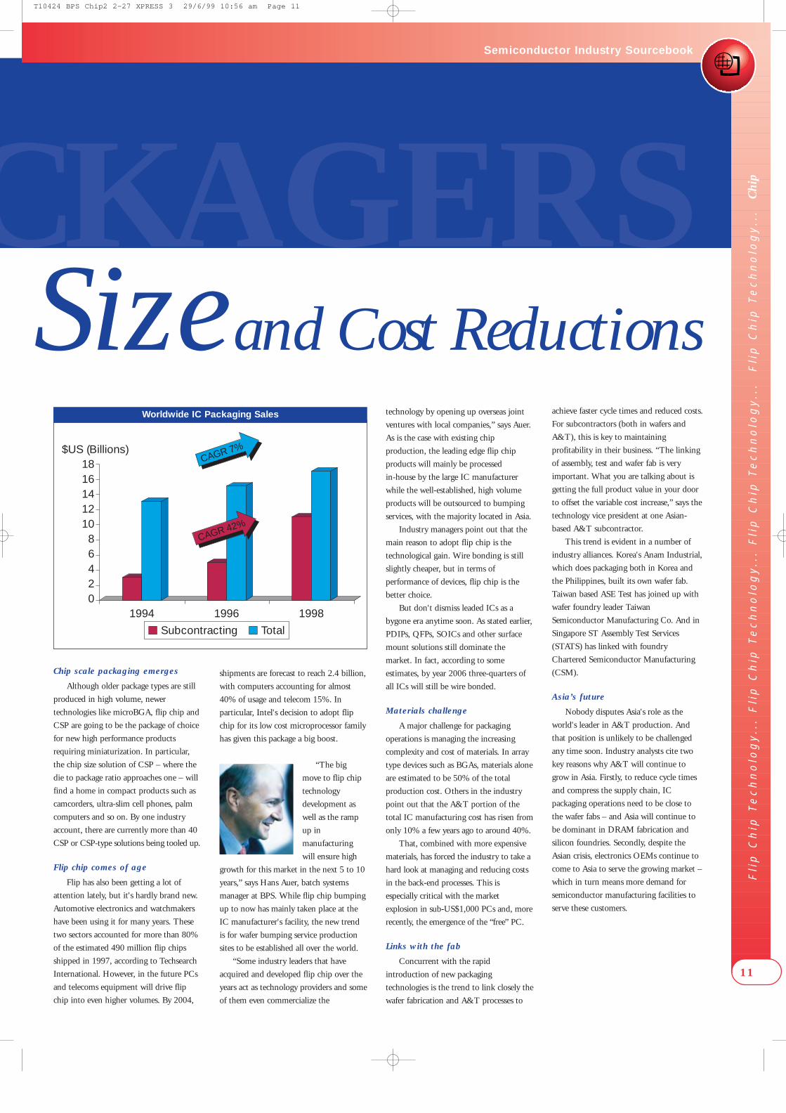
181614121086420
Subcontracting Total
$US (Billions)CAGR 7%
CAGR 42%
Worldwide IC Packaging Sales
Chip scale packaging emerges
Although older package types are still
produced in high volume, newer
technologies like microBGA, flip chip and
CSP are going to be the package of choice
for new high performance products
requiring miniaturization. In particular,
the chip size solution of CSP – where the
die to package ratio approaches one – will
find a home in compact products such as
camcorders, ultra-slim cell phones, palm
computers and so on. By one industry
account, there are currently more than 40
CSP or CSP-type solutions being tooled up.
Flip chip comes of age
Flip has also been getting a lot of
attention lately, but it's hardly brand new.
Automotive electronics and watchmakers
have been using it for many years. These
two sectors accounted for more than 80%
of the estimated 490 million flip chips
shipped in 1997, according to Techsearch
International. However, in the future PCs
and telecoms equipment will drive flip
chip into even higher volumes. By 2004,
shipments are forecast to reach 2.4 billion,
with computers accounting for almost
40% of usage and telecom 15%. In
particular, Intel's decision to adopt flip
chip for its low cost microprocessor family
has given this package a big boost.
“The big
move to flip chip
technology
development as
well as the ramp
up in
manufacturing
will ensure high
growth for this market in the next 5 to 10
years,” says Hans Auer, batch systems
manager at BPS. While flip chip bumping
up to now has mainly taken place at the
IC manufacturer's facility, the new trend
is for wafer bumping service production
sites to be established all over the world.
“Some industry leaders that have
acquired and developed flip chip over the
years act as technology providers and some
of them even commercialize the
technology by opening up overseas joint
ventures with local companies,” says Auer.
As is the case with existing chip
production, the leading edge flip chip
products will mainly be processed
in-house by the large IC manufacturer
while the well-established, high volume
products will be outsourced to bumping
services, with the majority located in Asia.
Industry managers point out that the
main reason to adopt flip chip is the
technological gain. Wire bonding is still
slightly cheaper, but in terms of
performance of devices, flip chip is the
better choice.
But don't dismiss leaded ICs as a
bygone era anytime soon. As stated earlier,
PDIPs, QFPs, SOICs and other surface
mount solutions still dominate the
market. In fact, according to some
estimates, by year 2006 three-quarters of
all ICs will still be wire bonded.
Materials challenge
A major challenge for packaging
operations is managing the increasing
complexity and cost of materials. In array
type devices such as BGAs, materials alone
are estimated to be 50% of the total
production cost. Others in the industry
point out that the A&T portion of the
total IC manufacturing cost has risen from
only 10% a few years ago to around 40%.
That, combined with more expensive
materials, has forced the industry to take a
hard look at managing and reducing costs
in the back-end processes. This is
especially critical with the market
explosion in sub-US$1,000 PCs and, more
recently, the emergence of the “free” PC.
Links with the fab
Concurrent with the rapid
introduction of new packaging
technologies is the trend to link closely the
wafer fabrication and A&T processes to
achieve faster cycle times and reduced costs.
For subcontractors (both in wafers and
A&T), this is key to maintaining
profitability in their business. “The linking
of assembly, test and wafer fab is very
important. What you are talking about is
getting the full product value in your door
to offset the variable cost increase,” says the
technology vice president at one Asian-
based A&T subcontractor.
This trend is evident in a number of
industry alliances. Korea's Anam Industrial,
which does packaging both in Korea and
the Philippines, built its own wafer fab.
Taiwan based ASE Test has joined up with
wafer foundry leader Taiwan
Semiconductor Manufacturing Co. And in
Singapore ST Assembly Test Services
(STATS) has linked with foundry
Chartered Semiconductor Manufacturing
(CSM).
Asia’s future
Nobody disputes Asia's role as the
world's leader in A&T production. And
that position is unlikely to be challenged
any time soon. Industry analysts cite two
key reasons why A&T will continue to
grow in Asia. Firstly, to reduce cycle times
and compress the supply chain, IC
packaging operations need to be close to
the wafer fabs – and Asia will continue to
be dominant in DRAM fabrication and
silicon foundries. Secondly, despite the
Asian crisis, electronics OEMs continue to
come to Asia to serve the growing market –
which in turn means more demand for
semiconductor manufacturing facilities to
serve these customers.
CKAGERSSize and Cost Reductions
T10424 BPS Chip2 2-27 XPRESS 3 29/6/99 10:56 am Page 11
Fli
p C
hip
Te
ch
no
log
y..
. F
lip
Ch
ip T
ec
hn
olo
gy
...
Fli
p C
hip
Te
ch
no
log
y..
. F
lip
Ch
ip T
ec
hn
olo
gy
...
Chip
Semiconductor Industry Sourcebook
12
Progress in Flip Chip
By Hans Auer, Batch Systems Manager, BPS Trübbach
While many of the most sensitive devices are still packaged with IBM’s original
evaporative C4 process, today’s state of the art flip chip process is emerging as a sputtered
or evaporated blanket film UBM with electroplated solder bumps. This is just one
highlight of the ongoing technology development in flip chip packaging.
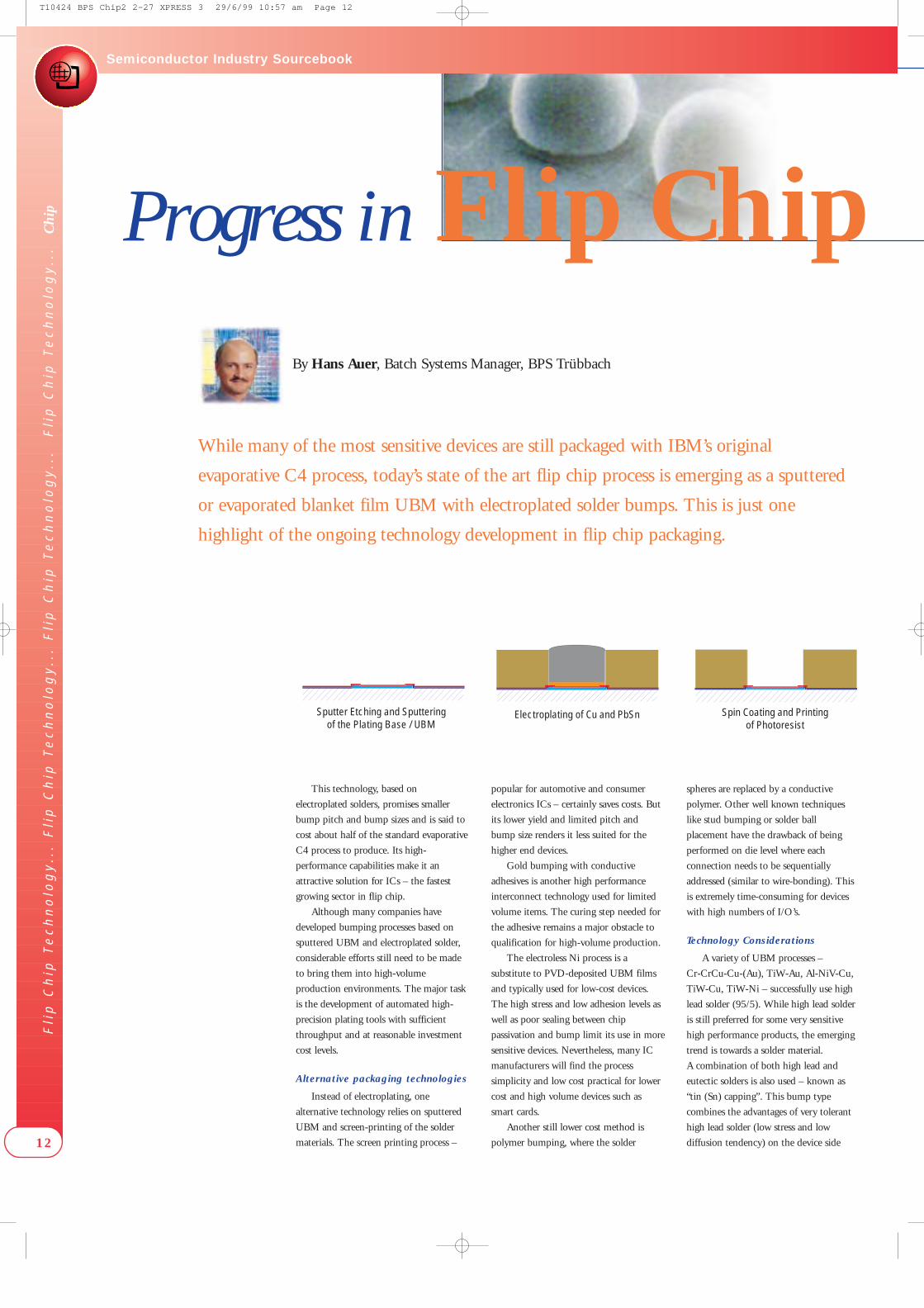
This technology, based on
electroplated solders, promises smaller
bump pitch and bump sizes and is said to
cost about half of the standard evaporative
C4 process to produce. Its high-
performance capabilities make it an
attractive solution for ICs – the fastest
growing sector in flip chip.
Although many companies have
developed bumping processes based on
sputtered UBM and electroplated solder,
considerable efforts still need to be made
to bring them into high-volume
production environments. The major task
is the development of automated high-
precision plating tools with sufficient
throughput and at reasonable investment
cost levels.
Alternative packaging technologies
Instead of electroplating, one
alternative technology relies on sputtered
UBM and screen-printing of the solder
materials. The screen printing process –
popular for automotive and consumer
electronics ICs – certainly saves costs. But
its lower yield and limited pitch and
bump size renders it less suited for the
higher end devices.
Gold bumping with conductive
adhesives is another high performance
interconnect technology used for limited
volume items. The curing step needed for
the adhesive remains a major obstacle to
qualification for high-volume production.
The electroless Ni process is a
substitute to PVD-deposited UBM films
and typically used for low-cost devices.
The high stress and low adhesion levels as
well as poor sealing between chip
passivation and bump limit its use in more
sensitive devices. Nevertheless, many IC
manufacturers will find the process
simplicity and low cost practical for lower
cost and high volume devices such as
smart cards.
Another still lower cost method is
polymer bumping, where the solder
spheres are replaced by a conductive
polymer. Other well known techniques
like stud bumping or solder ball
placement have the drawback of being
performed on die level where each
connection needs to be sequentially
addressed (similar to wire-bonding). This
is extremely time-consuming for devices
with high numbers of I/O’s.
Technology Considerations
A variety of UBM processes –
Cr-CrCu-Cu-(Au), TiW-Au, Al-NiV-Cu,
TiW-Cu, TiW-Ni – successfully use high
lead solder (95/5). While high lead solder
is still preferred for some very sensitive
high performance products, the emerging
trend is towards a solder material.
A combination of both high lead and
eutectic solders is also used – known as
“tin (Sn) capping”. This bump type
combines the advantages of very tolerant
high lead solder (low stress and low
diffusion tendency) on the device side
Sputter Etching and Sputteringof the Plating Base / UBM
Electroplating of Cu and PbSn Spin Coating and Printingof Photoresist
T10424 BPS Chip2 2-27 XPRESS 3 29/6/99 10:57 am Page 12

done in the following assembly steps.
A memory chip has much lower
requirements than a microprocessor that
operates at higher temperatures, making
diffusion resistance a higher priority.
Business of Packaging
Today, the usual way for most
companies wishing to start with flip chip
bumping is through a license/technology
partnership with a qualified technology
provider. Usually, research institutes or
large, well-known IC manufacturers
license their packaging know-how together
with a process transfer/support package.
Many bumping fabs are vertically
integrated within large
IC
manufacturing companies or function as
foundries for the sole purpose of selling
bumping services, sometimes with added
services such as testing. They are often
joint ventures with one partner as the
technology provider and the other(s)
providing manufacturing know-how and
an established base in the respective area
of the manufacturing site.
For further information on how to
ramp-up a flip chip packaging process,
contact us at: [email protected]
with the low melting temperature of
eutectic solder on the carrier or PC board
side.
The eutectic solder presents a new
hurdle for some of the existing UBM
metallurgies. Since much more Sn is
available, the requirements for the barrier
properties are much higher – to prevent
Sn diffusion. Some applications solve this
problem by adding several microns of
electroplated Cu to the UBM. Others use
Ni to inhibit diffusion of Sn more
effectively than Cu. On the other hand,
Ni with Sn forms much higher stress
inter-metallics than Cu and Sn.
A further method is to increase the
thickness of the CrCu compound film.
Requirements for this barrier are also
influenced by test specifications, in this
case a number of reflow steps. The range
is anywhere from 5 to 20 (or even more)
reflow steps. Of course, these
specifications are based on device
requirements and the number of reflows
Fli
p C
hip
Te
ch
no
log
y..
. F
lip
Ch
ip T
ec
hn
olo
gy
...
Fli
p C
hip
Te
ch
no
log
y..
. F
lip
Ch
ip T
ec
hn
olo
gy
...
Chip
Semiconductor Industry Sourcebook
13
pwettable metallization (ep-Cu)
plating base (Cu)
adhesion layer and diffusionbarrier (Ti:W)
passivation (Si02, Si3N4, SiON)
VO-pad (AI)
chip (Si)
Pb40Sn60Pb95Sn5
Resist Stripping and Wet Etchingof the Plating Base
Reflow
PACKAGING TECHNOLOGY
Leading Bumping Service Companies:
– APACK, Hsin-chu, Taiwan
– APTOS, Milpitas (CA), USA
– Chipbond, Hsin-chu, Taiwan
– Flip Chip Technologies, Phoenix, USA
– Focus Interconnect, Austin (TX), USA
– FUPO Electronics, Hsin-chu, Taiwan
– IC Interconnect, Colorado Springs
(CO), USA
– MicroFab, Technology, Singapore
– Pac Tech, Nauen, Germany
– Polymer Flip Chip, Billerica (MA), USA
– Unitive Electronics, Research Triangle
Park (NC), USA
Source: technology news
T10424 BPS Chip2 2-27 XPRESS 3 29/6/99 10:57 am Page 13

Fli
p C
hip
Te
ch
no
log
y..
. F
lip
Ch
ip T
ec
hn
olo
gy
...
Fli
p C
hip
Te
ch
no
log
y..
. F
lip
Ch
ip T
ec
hn
olo
gy
...
Chip
Semiconductor Industry Sourcebook
14
Volume Production S
By Andreas Dill, Cluster Systems Manager, Hans Auer, Batch Systems Manager, and Martin Märk, Product Specialist, BPS Trübbach
A complete overview by system type
BPS has supplied under bump metallization (UBM) coating systems since the advent of flip chip over
30 years ago. This overview of all dedicated system types currently offered by BPS provides a wide range
of production solutions with respect to specific UBM structures, substrate sizes and substrate mixes.
Back then, evaporated layers of
Cr-CrCu-Cu-Au were used in the original
C4 concept. Several years ago batch
sputtering systems for UBM were added
(the LLS series). More recently, all major
UBM processes were also implemented on
a single wafer processing system (the
CLUSTERLINE 200).
Our product portfolio is constantly
being optimized and extended to provide
ideal mass-production solutions. The new
systems provide higher throughputs at
constant running costs, reducing the costs
of ownership (CoO). This year, BPS
introduced the HIPACK, a batch
sputtering system with the industry’s
lowest cost per wafer for specific UBM
structures. At the same time, our new
300mm cluster tool was introduced for
the new form factor and is also available as
a bridge tool.
All current UBM processes are
supported on the complete product
portfolio. This covers the following
processes:
Cr-CrCu-Cu-Au (original C4)
TiW(N)-Cu-Au
TiW(N)-NiV-Au
Cr-NiV-Au
Cr-Cu-Cr-NiV-Au
Cr-Cu-Au
Al-NiV-Cu
Please note that the final Au layer is no
longer used in many UBM applications
Overall, the process advantages with all
production solutions from BPS include:
Evaporation Systems for UBMEspecially for the classical C4 process, our
BAK series of evaporators represent the
industry standard for UBM applications.
New UBM processes and rerouting steps
have been added and today we offer
complete wafer bumping production
solutions based on evaporation systems.
Even though the lift-off process
(directional coating) is a specific advantage
of the evaporators, blanket film deposition
applications are also possible.
The typical evaporation process
sequence is:
1. Preheat
2. RF sputter clean etch
3. Evaporation sequence (including
heating)
● Oxide free IC final metal pads (Al)● Excellent adhesion to metal pad and
chip passivation● Good diffusion barrier including
phasing layer● Sufficient wetability of UBM for
stable solder re-flow● Low stress layer stack for long time
reliability
Depending on the UBM application,
BPS offers the following system types for
UBM mass-production profiled here:
– Evaporation systems
– Batch sputter systems
– Cluster tools
Typical evaporation process sequence
(BAK FLIPACK)
1. Preheat 250°-300°C
2. RF etching 15nm, at 0.025nm/sec.
3. Evaporation of Cr 100nm, at 0.5nm/sec.
4. Evaporation of CrCu 200nm, at 0.5nm/sec.
5. Evaporation of Cu 800nm, at 1.0nm/sec.
6. Evaporation of Au 50nm, at 0.5nm/sec.
T10424 BPS Chip2 2-27 XPRESS 3 29/6/99 10:58 am Page 14

Fli
p C
hip
Te
ch
no
log
y..
. F
lip
Ch
ip T
ec
hn
olo
gy
...
Fli
p C
hip
Te
ch
no
log
y..
. F
lip
Ch
ip T
ec
hn
olo
gy
...
Chip
Semiconductor Industry Sourcebook
15
n Solutions for UBMThe new BAK FLIPACK system
The BAK FLIPACK is the latest addition
to the BAK series and is the result of a
complete redesign of the successful BAK
1131. The main objectives of the redesign
were:● Higher throughput● Lower cost of ownership (CoO)● Greater process reliability● Increase batch size and maintain
substrate size flexibility
In more detail, the BAK FLIPACK
features:● Increased process reliability –
Redundant pumping systems (2) and
redundant sources, with up to five
back-up crystals in the rate and
thickness monitoring system● Better material utilization – 20%
improvement for standard materials,
and 40% for gold – due to flexible
positioning of the evaporation sources
closer to the substrates● Identical overall running costs – Power
usage, water and other commodities
are identical to the smaller BAK 1131
model● Increased floor space utilization –
While the system layout is only 10%
larger than the previous model,
throughput is increased by 35%,
giving an overall floor space reduction
of >20%
Compared to the BAK 1131, the CoO
for the FLIPACK is significantly reduced.
It is the ideal evaporation system for high
throughput requirements.
Total clean room compatibility with
BAK EVO
Based on the industry-standard BAK
system platform, the BAK EVO features a
comprehensive update of both the
hardware and software performance
parameters to meet today’s stringent clean
room and production standards.
Advantages of evaporation systems
The advantages of evaporation in UBM
are maintained with the BAK systems and
BAK FLIPACK:● Cr-Cu phasing with continuous
gradation/degradation of both
materials● Substrate size flexibility● Lift-off processes● Highest process flexibility
● Changes in materials and their
sequence within minutes
The BAK series of evaporators feature
the following performance specifications:
Batch capacities/ Throughput/
wafer size (wafers/h)
BAK EVO 8 / 200 mm 5
18 / 150 mm 11
BAK FLIPACK 25 / 200 mm 14
50 / 150 mm 28
All throughput figures are based on
the following process parameters. The
same values are used for all systems,
etching is used only with sputtering systems.
Etch 10 nm
Cr 100 nm
CrCu (50% Cu) 200 nm
Cu 500 nm
Batch Sputter Systems for UBMThe unique rotating drum design of the
BPS batch sputter systems allows
co-deposition of two independent
materials to create high-quality phase-ins
as required in the original C4 UBM
process. The systems have proven
extremely reliable in 7 x 24 production
environments.
The typical sputter process sequence is:
1. Degassing
2. RF sputter clean etch or Ion Etch/Mill
3. Sputter process with co-sputtering
The high-throughput HIPACK system
The HIPACK batch sputter system from
BPS features an exceptionally high
throughput at the lowest cost per coated
area. It is a highly dedicated UBM system
and eschews the extra features not
required for this process, such as a load
lock or automated handling option. With
proven production and process reliability,
the HIPACK is a welcome addition to all
UBM applications. Intended for substrate
sizes of up to 400mm (round or square),
the HIPACK provides a very low cost per
wafer as well as a low capital investment,
with throughput well within the range of
single wafer tool configurations.
Compared to the throughput capacity
of the HIPACK, the footprint is very
compact. Including all auxiliary
equipment, the system footprint is only
3.5 m wide and 5 m deep.
Typical sputter process sequence (LLS EVO)
1. Wafer degassing 150-200° C
2. Sputter etch 5-10 nm, removal of oxides
3. Sputter Cr 100 nm, 30 nm/min at 4kW
4. Sputter CrCu 80 nm co-sputtering
multi-layering of CrCu
(➔ Inter-diffusion)
e.g. Cr – 7nm/min at 1kW
Cu – 12nm/min at 1kW
fast rotation of substrate
carrier drum max.
rotational speed
= 30 rpm
5. Sputter Cu 400nm, at 72nm/min at
6kW.
6. Sputter Au 50nm, at 20nm/min at 2kW
T10424 BPS Chip2 2-27 XPRESS 3 29/6/99 10:58 am Page 15

Fli
p C
hip
Te
ch
no
log
y..
. F
lip
Ch
ip T
ec
hn
olo
gy
...
Fli
p C
hip
Te
ch
no
log
y..
. F
lip
Ch
ip T
ec
hn
olo
gy
...
Chip
Semiconductor Industry Sourcebook
16
Process dynamics
Short cycle times and high deposition
rates are among the success factors of the
HIPACK. The system’s unique “rotating
drum” design allows co-deposition of two
different materials. The HIPACK can
consistently produce perfect phase-in layers,
such as with the long term field-proven
LLS tools.
KHAN NT control system
The HIPACK sputter system features
the Windows™ NT-based KHAN NT
system controller. Successfully used in the
BAK evaporation systems, the standard
control system assures a high degree of
operation reliability of the tool.
Ultimate process flexibility with
LLS EVO
Based on the field-proven LLS platform,
the LLS EVO features improved system
control and process software to simplify
running a remarkable range of
applications (UBM, MEMs, MCM, TFH,
thin film resistors, power devices and
optical integrated circuits). These en-
hancements are backward compatible to
previous LLS 502 systems already in use.
Advantages of batch sputter systems
These general advantages of our batch
sputter systems apply also to the
HIPACK:● Flexibility in substrate size● Highest process flexibility● Nearly unlimited choice of layer
sequences● Co-sputtering● Material phasing
Our line of batch sputter systems
feature the following performance
specifications:
Batch capacities/ Throughput/
wafer size (wafers/h)
HIPACK 28/200 mm wafers 24
54/150 mm wafers 46
LLS EVO 9/200 mm wafers 12
12/150 mm wafers 16
Cluster Tools for UBMThe increasing trend towards larger wafer
sizes has also increased demand for cluster
tools for UBM. Extensive process
experience and application work for
different customers lead to a system
combining high volume production with
high reliability. We achieve the best Cr:Cu
mixture properties thanks to the
proprietary compound Cr:Cu target. The
positive feedback from many clients has
also led to development of a 300mm
cluster tool configuration.
The typical cluster tool process
sequence is:
1. Degassing
2. RF soft sputter etch
3. Sputter process according to the layer
sequence. (Up to four PVD modules
can be used with this process
sequence.)
The CLUSTERLINE 200 high
throughput cluster tool
The CLUSTERLINE 200 is a
metallization tool that meets all
requirements for the advanced wafer fab.
This tool features excellent automated
factory integration, a modular design for
flexible process configuration, low
contamination and superior process
control thanks to the ControlWORKSTM
control system.
The greatest advantage of the
CLUSTERLINE is a high throughput of
more than 40 wafers per hour for the
UBM process, independent of wafer size.
For large 200mm and 300mm wafers, the
CLUSTERLINE provides a remarkably
low cost of ownership.
Process dynamics
The typical Cr-Cr:Cu-Cu-Au UBM
process sequence on the CLUSTERLINE
200:
1. Wafer degassing 200°-300°C
2. ICP soft clean etch 5-10nm, removal
of oxides
3. Sputter Cr 100nm, 7nm/sec at
5kW single wafer
static sputtering
4. Sputter Cr:Cu 80nm, 15nm/sec at
3.5kW proprietary
Balzers target
5. Sputter Cu 400nm, 30nm/sec
at 10kW
6. Sputter Au 50nm, 6nm/sec at
2kW
The new, larger CLUSTERLINE 300
The newly introduced CLUSTERLINE
300 features the same system and process
capabilities as the 200mm cluster tool and
promises to be every bit as effective. The
product team has optimized the respective
UBM processes for 300mm wafers.
The system layout of the larger
CLUSTERLINE 300 is based on field-
proven components, such as the handling
robot and process elements, as well as the
PC-based ControlWORKS system
software. This assures uptime reliability
equal to the CLUSTERLINE 200
systems. The new tool is also available as
bridge tool, offering a smooth transition
from 200mm to 300mm wafer
production. Phasing processes such as the
Cr:Cu process are realized with
proprietary compound sputter targets.
Advantages of Cluster Tools for UBM
In addition to the above-noted benefits,
the CLUSTERLINE tools also feature:● E-chuck for precise temperature
control and reduced edge exclusion● Optimized sources for high target
utilization and excellent layer
uniformity● Precise temperature management● Throughput virtually independent of
wafer size (with appropriate design)● Low cost of ownership for UBM
processes with 200mm or 300mm
wafer sizes
The CLUSTERLINE family of single
wafer sputter systems feature the following
performance specifications:
Batch capacities/ Throughput/
wafer size (wafers/h)
CLUSTERLINE 200
Single wafer/200 mm 45
Single wafer/150 mm 45
CLUSTERLINE 300
Single wafer/300 mm 45
Typical Cr-Cr-Cu-Au UBM process sequence
(CLUSTERLINE 200)
1. Wafer degassing 200-300° C
2. ICP soft clean etch 5-10 nm, removal of oxides
3. Sputter Cr 100 nm, 7 nm/sec at 5 kW,
single wafer static
sputtering
4. Sputter CrCu 80 nm; 15 nm/sec at 3.5 kW,
proprietary Balzers target
5. Sputter Cu 400 nm; 30 nm/sec at 10 kW
6. Sputter Au 50 nm; 6nm/sec at 2kW
T10424 BPS Chip2 2-27 XPRESS 3 29/6/99 10:58 am Page 16

Cost of Ownership, Depending on Wafer Production(UBM; Process: Cr - Cr:Cu - Cu; 200 mm Wafer)
Cost of Ownership, Depending on Wafer Production(UBM; Process: Cr - Cr:Cu - Cu; 150 mm Wafer)
Wafer production per hour
Wafer production per hour
BAK EVO
BAK EVO
BAK EVO
BAK EVO
BAK FLIPACK
BAK FLIPACK
BAK FLIPACK
LLS EVO
LLS EVO
CLUSTERLINE 200/300
NEXTRAL 500
BAK FLIPACK
ORF 901
ORF 901
LLS EVO HIPACK
HIPACK
HIPACK
HIPACK
LLS EVO
CLUSTERLINE 200/300
CLUSTERLINE 200/300
BA
K E
VO
Processes
UBM– Sputter Clean
– Sputter deposition
– Evaporation
PbSn Solder Bumps
Rerouting
Carrier preparation/PC board preparationand build-up
BA
K F
LIPA
CK
OR
F 90
1
LLS
EVO
CLUS
TERL
INE 2
00/3
00
HIP
AC
K
NEX
TRA
L 50
0Packaging Systems andApplications
Fli
p C
hip
Te
ch
no
log
y..
. F
lip
Ch
ip T
ec
hn
olo
gy
...
Fli
p C
hip
Te
ch
no
log
y..
. F
lip
Ch
ip T
ec
hn
olo
gy
...
Chip
Semiconductor Industry Sourcebook
17
Cost of ownership (CoO)comparisons for differentsputter systemsThe comparison of CoO models for
various process system types is relevant to
the manufacturer for:● Product benchmarking● Technology evaluation● Process optimization● Impact of materials● Competitive analysis● Sales / purchase parameters
Simplified models as a quantitative
management technique are used to analyze
purchasing decisions, standard cost analysis
and equipment prioritization. Less suitable
for absolute cost calculation, they can be
used to compare different system layouts.
Here we consider the cost of ownership
for UBM based on the Cr-Cr:Cu-Cu
process for 150mm and 200mm wafers.
As mentioned above, etching is used only
with sputtering systems.
The cost of ownership for this process
depends on the different running costs of
the individual systems:
a. General financing and overhead costs
(system cost, interest rates, space costs,
personnel costs, etc.)
b. Variable costs per hour (materials,
power, etc.)
c. Throughput numbers and real wafer
production per year
d. Number of systems needed to meet
production goals
Four different systems show different
strengths: The cost of ownership for these
four systems depends on the hourly
production rate of the wafers. Obviously,
the choice of a particular system depends
not only on the cost of ownership, but
also on other factors such as wafer
handling capabilities (i.e. manual loading,
cassette-to-cassette loading, etc.) or wafer
logistics (wafer flow).
On batch systems (evaporation and
sputtering), the costs per wafer increase
considerably with the wafer size and
production volume. With cluster tools,
the cost per wafer remains more or less
independent of wafer size.
The degree of cost variations depends
also on the number of systems needed to
achieve the desired production capacity.
These cost variations can differ greatly
between system types. Careful
consideration must be given to the CoO
values for each given production figure.
depending on batch capacity.
For more information on cost of
ownership evaluations, please contact
us at: [email protected].
T10424 BPS Chip2 2-27 XPRESS 3 29/6/99 11:02 am Page 17

MetalliThe immense boom in the
automotive, telecom and
consumer electronics markets has
led to equally growing pressure for
higher yields and throughput for
manufacture of discrete and power
devices. This is precisely where
backside metallization of thin
wafers plays a central role for the
device manufacturer. Here
we look at a new sputtering
solution for backside
metallization with thin
wafer processing
capabilities.
Fro
nt
en
d m
an
ufa
ctu
rin
g..
. F
ron
t e
nd
ma
nu
fac
turi
ng
...
Fro
nt
en
d m
an
ufa
ctu
rin
g..
. Chip
Semiconductor Industry Sourcebook
18
Thin wafer processing on the CLUSTERLINE
Packed with thousands of transistors,
capacitors and resistors together with active
and passive elements on a single chip,
state-of-the-art integrated circuits pose
substantial production challenges. Backside
metallization enables sufficient electrical
conductivity punched through the wafer to
connect to the chip backside – typically
used in discrete and power devices.
Going from evaporation to
sputtering
In discrete and power device
manufacturing, one can still find a wide
range of wafer sizes, from 4" to 6" and
even 8" substrates in common use. In fact,
it’s possible to see many different substrate
A standard substrate size encourages
higher throughput demands, which favors
a single wafer cluster tool design with its
distinctly higher throughput.
The second reason for the trend to
sputtering is the growing use of thinner
wafers, as employed for new processes for
discrete ICs and power devices. A thinner
wafer is more prone to breakage, raising
production costs. A single wafer tool with
an automated handling system is the only
way to reliably meet higher throughput
goals, making handling and processing of
thin wafers a key strategic technology for
future device manufacturing.
Today, while most backside
applications are coated with batch
14
12
10
8
6
4
Str
ess
[E9
dyn/
cm2 ]
2
0
-2
-4
-60 50 100 150 200 250 300 350 400 0
Temp [°C]
Ni
Ti
Au
Film stress for different materials with backside metallization.
sizes being processed in the same fab line.
Processing different wafer sizes in the same
run plays to the flexibility of a batch
evaporation tool.
However, production technology is
clearly moving away from evaporation and
towards increased use of sputtering. There
are a couple of reasons for this. First off,
the device manufacturers are moving to
larger wafer sizes – with 6" and 8" wafer
diameters as the emerging norm.
evaporation tools, cost of ownership
calculations for wafer sizes of 6" and larger
have shown the cost per sputtered wafer to
be roughly half of a wafer coated in a
batch evaporation system.
New thin wafer processing tool
Working together with Brooks
Automation and key commercial partners,
BPS has focused considerable
development resources during the past
Moving Up with
Backside Metallization By Dr. Reinhard Benz, Product ManagerSemiconductors, BPS Trübbach
T10424 BPS Chip2 2-27 XPRESS 3 29/6/99 11:03 am Page 18

Full house: The BPS CLUSTERLINE assembly line in Switzerland.
ization
Fro
nt
en
d m
an
ufa
ctu
rin
g..
. F
ron
t e
nd
ma
nu
fac
turi
ng
...
Fro
nt
en
d m
an
ufa
ctu
rin
g..
. Chip
Semiconductor Industry Sourcebook
19
year with the optimization of a sputtering
solution for backside metallization with
thin wafer processing capabilities.
“Our newest
cluster tool
features an
extremely
dependable
handling and
transport system
capable of
transporting and
processing thin
and ultra thin
substrates,” explains Gernold Engstler,
cluster systems project manager at BPS.
“This not only reduces breakage. It is
especially important for reliable backside
metallization processes for thinned wafers,
such as (Al)-Ti-Ni(V)-Ag.”
Metallization system highlights
A typical backside metallization process
begins with an adhesion layer (Ti or Cr),
then continues with barrier layers (Ni, Ni-
V or TiV) and top layer metals (Ag or Au).
Electrostatic clamping in the soft etch and
sputter modules ensure excellent process
conditions for the thinner wafers. With no
mechanical contact between the clamping
and shielding elements, the electrostatic
chuck assures very efficient gas conduction
for backside cooling or heating of thin
wafers. This results in improved
temperature conductivity and uniformity
over the wafer surface to enable lower
stress. Such process parameters allow
application of higher sputtering power
with less contamination leading to higher
throughput.
Also, the integrated wafer handling
hardware capably handles typical thin
wafer thickness ranges of 150 mm, used in
150mm Ø wafers – and 200 mm, used for
200mm Ø wafers. Additional performance
parameters include improved wafer
sensoring and wafer alignment for the
different thickness of ultra-thin wafers.
Successful market ramp-up
Final tests at the BPS labs included
running over a thousand silicon wafers
through a typical configuration for
backside metallization, where wafer
alignment, pretreatment and PVD
performance were also analyzed. All wafers
were processed without any electrical
damage (usually caused by electrostatic
clamping) and handled without any
breakage or visible scratching. More
recently, initial acceptance tests at
customer sites in Europe have produced
promising results. Demand and interest in
a sputtering system solution with thin
wafer processing remains high. We will
continue to deliver further systems to
customers throughout the year.
Works with GaAs
The system design for both thinned Si
wafers and notoriously brittle GaAs wafers
sets similar performance demands on
handling and processing capabilities. But if
the automated thin wafer handling hardware
in the CLUSTERLINE cluster tool is
appropriate for thin Si wafers and GaAs
wafers, it is really stress control that is the
critical process parameter for physical
handling. Also, GaAs wafers are extremely
sensitive to stress during the metallization
process. A consistent and controllable
temperature transition between the
electrostatic chuck and the substrate is
extremely important. Our recent
CLUSTERLINE system ramp-up with a
large European key account is setting new
standards in metallization of GaAs wafers.
If you need more information on our
backside metallization processes, please
contact us at [email protected].
“”
BPS has focused considerable
development resources on the
optimization of backside metallization
with thin wafer processing capabilities.
Software Issues with ClusterTools for IC Manufacturing
By Rudolf Schmuki, Cluster Tool Specialist, BPS Trübbach
Working for over a decade with cluster tool systems and
processes has brought BPS valuable experience in both the
hardware and software sides of mass-production solutions
used on our CLUSTERLINE system. Here we look at some
of the issues encountered with software development.
Development of our first cluster tool
platform (the CLC 9000) began in 1987,
which was followed by the launch of the
CLUSTERLINE series in 1996. The
original control software used in these
tools was developed and tested by BPS
using Pascal programming language and
the ELN real-time operating system from
DEC.
Today, our system control software is
based on ControlWORKS* from Adventa
Control Technology. The framework of
this software package provides the most
common request commands used with on
a cluster tool in IC manufacturing. Our
in-house software development group adds
specific process procedures and other
customer requirements. In general, using a
standardized, off-the-shelf cluster tool
control software package provides the
equipment manufacturer with:● Shorter development time for quicker
product availability● Compliance to semiconductor
industry standards ● Easy implementation of new process
module types ● Integration of modules from other
suppliers
In turn, the system owner benefits
from a field-proven control system, in
particular because many other equipment
manufacturers use software packages such
as ControlWORKS. This control system is
widely considered a de facto standard for
cluster tool applications. Further benefits
include: ● Customization – An open structure
allows the addition of very specific
customer requirements (such as
individual operator screens or
additional functionality).● Wafer scheduler – To meet both R&D
and production needs, it enables
multiple process runs in the same
chamber and specific throughput
controls.● Additional modules – Additional SW
package modules – for advanced
process control, automated process
tracking (for simplified preventive
maintenance) are available from
Adventa.
Basing our control and process software
on ControlWORKS gives BPS the
advantage of a reliable, widely accepted
software package that works flawlessly with
the CLUSTERLINE hardware for an ideal
mass-production solution.
*For more information on
ControlWORKS, look up
www.adventact.com on the Internet.
T10424 BPS Chip2 2-27 XPRESS 3 29/6/99 11:03 am Page 19

Multi-Level Metallization
Multi-Level MetallizatiMulti-Level Metallizatio
Fro
nt
en
d m
an
ufa
ctu
rin
g..
. F
ron
t e
nd
ma
nu
fac
turi
ng
...
Fro
nt
en
d m
an
ufa
ctu
rin
g..
. Chip
Semiconductor Industry Sourcebook
20
Multi-Level Metallization
By Dr. Reinhard Benz
Interconnects using
RTP annealing steps
have a bright future in
ASIC and discrete
devices used in
automotive, telecom
and consumer
electronic products.
Here we present
alternatives for
ramping-up RTA/RTP
processing – an
integrated reactor in the
CLUSTERLINE
system platform and a
stand-alone XT 80
system module.
Everybody talks about copper, but
aluminum is still the most widely used
metallization material for IC
interconnects. Despite the widespread use
of Al, some of its shortcomings demand
attention: poor electro-migration, poor
stress characteristics and interactions with
silicon at relatively low temperatures
(@450°C). Adding a small percentage of
silicon improves junction spiking, adding
copper reduces electro-migration and
stress-induced hillocks.
The barrier layer between the
aluminum and the silicon contact gives a
structure with low contact resistance and
no degradation of the shallow junction
device integrity during sequential thermal
cycles. The most widely-used stack is still
a thin titanium film followed by titanium
nitride (Ti/TiN) or titanium-tungsten
(TiW). To improve the barrier
performance and reliability, annealing
steps in an integrated RTP module using
N2 or N2/O2 atmosphere are introduced.
Salicidation in the RTP module
In the salicide process a deposited
Ti/N film is thermally reacted in an N2
ambient to form a thin silicide film on
gates and source/drain areas (formation
step). Initially, a high resistivity meta-
stable phase of about 90 mohm cm with a
C49 crystal structure is formed, followed
by the thermodynamically stable low
resistivity C54 phase (about 15 mohm cm).
During this anneal step the Ti Si2 forms
the C54 phase to achieve low sheet
for IC Inter cPVD metal l izat ion with an integrated R
CLUSTERLINE 200 with an integrated RTP module (upper right).Temperature range: 300°C - 1200°C
Temperature calibration: ±5°C
Temperature uniformity at 1000°C: ±2°C (at 800°C)
Temperature repeatibility at 1000°C: ±2°C
Temperature stability at 1000°C: ±1°C (for >1 hour)
Max. ramp-up rate on Si wafer: 80°C/sec with regulation
Wafer cooling under N2 flux (Si): > 50°C/sec between 600-400°C
Temperature overshoot: < 5°C at max. ramp rate
RTP cluster tool module performance specifications
T10424 BPS Chip2 2-27 XPRESS 3 29/6/99 11:03 am Page 20

on
ation ionr connectsd RTA/RTP module
Fro
nt
en
d m
an
ufa
ctu
rin
g..
. F
ron
t e
nd
ma
nu
fac
turi
ng
...
Fro
nt
en
d m
an
ufa
ctu
rin
g..
. Chip
Semiconductor Industry Sourcebook
21
A Stand-Alone Solution for
Based on the RTP module used in the CLUSTERLINE
cluster tool, the RTP 80 stand-alone system ensures excellent
uniformity of process temperature and suitable for R&D and
production environments.
The RTP 80 System
“We have over
19 years of experience
with RTP. Our know-
how helped us work
together with BPS to
launch a fully integrated RTP module for
the CLUSTERLINE – and also optimize
a stand-alone RTP furnace,” says Pierre
Parrens, president of BPS-Nextral. “Both
the integrated and stand-alone solutions
are based not only on the same process,
but also the same system components.”
Inside the system
The RTP light source with a water-
cooled reflector assembly is made of pure
polished aluminum for optimum
reflection of infra red radiation. It is
equipped with 24 high intensity halogen
lamps arranged in two perpendicular
arrays to achieve excellent temperature
uniformity. The lamps and their
connections are fan-cooled.
Thyristors, phase angle controllers,
and intensity transformers for current
measurements were mounted on the top
part of the furnace. A shielded enclosure
protects everything for safety and to
eliminate any electrical disturbance. The
top part of the furnace is mounted on a
hinge to facilitate servicing. All these
features and lamp positioning were
optimized to perform according to the
specifications below.
RT Presistance and meet device performance
requirements.
Salicidation in the Si contact area has
two major effects:
1. The Ti seed layer is converted nearly
completely to TiSi2, resulting in a
lower contact resistance.
2. The grain boundaries of TiN are
annealed and stuffed (depending on
the residual gas), leading to improved
barrier characteristics and higher
temperature stability.
The RTP module specifications
The RTP process module is optimized
for 6" and 8" wafers, has a cold wall
reactor with a heater block using IR lamps
up to 55 kW. Two pyrometers or optional
thermocouplers control the temperature
level. The wafer is heated through an air-
cooled quartz plate by several independent
heating zones to give excellent
temperature uniformity over the wafer
area. A special turbo-pumping package
and gas inlet system enables quick
pumping rates and high purging speeds to
assure very consistent process conditions.
Built for fast processing and high
process reproducibility, the RTP module
relies on a closed-loop numerical PID
controller to maintain faultless
performance characteristics.
The advantages of integration
Integrating the RTP module into the
CLUSTERLINE cluster tool offers tangible
advantages to the IC manufacturer.
Reduced wafer contamination and
consistently high process reproducibility are
key features of the vacuum-integrated
thermal process. Also, the resulting low
thermal budget and improved temperature
uniformity are essential for critical designs
below 0.18mm, and especially for
production on 300 mm wafers. Obviously,
all these factors, combined with the process
flexibility of the cluster tool layout,
contribute positively to the cost of
ownership for the CLUSTERLINE.
For more information on the
RTA/RTP processes and reactor, please
contact us at [email protected]
Heat-up phase of the quartz lamp arrangementin the RTP module of the CLUSTERLINE 200.
Before and after the RTP annealing step:Cross Sections of multi-layer structures.Before salidication: The Ti-TiN-Ti multi-layerstructure on an Si wafer shows the typicalbarrier stack with a Ti seed layer, a TiN barrierand a Ti capping layer.After annealing: The TEM cross section isshown after annealing at approximately700°C in a N2/O2 atmosphere.
We have over
19 years of experience with RTP. Our
know-how helped us work together
with BPS to launch a fully integrated
RTP module for the CLUSTERLINE –
and also optimize a stand-alone RTP
furnace.
“
”C
Stand-alone RTP module performance specifications
– Temperature range (Si wafer) 350 to 1200°C (1 pyrometer)
– Temperature range (Si wafer) 500 to 1200°C (1 pyrometer)
– Temperature uniformity ± 0,5% (at 1,000°C)
– Temperature stability ± 1°C (For >1 hour)
– Temperature repeatability ± 2°C
– Temperature ramp-up/Si wafer 80°C/sec
TEM photoscourtesy of NMI
T10424 BPS Chip2 2-27 XPRESS 3 29/6/99 11:03 am Page 21

Fro
nt
en
d m
an
ufa
ctu
rin
g..
. F
ron
t e
nd
ma
nu
fac
turi
ng
...
Fro
nt
en
d m
an
ufa
ctu
rin
g..
. Chip
Semiconductor Industry Sourcebook
22
Standard electronic memories are
based on electron currents and charges in
semiconductors. For example, SRAMs
(static RAM) have a “flow through”
design, whereas a DRAM works with a
“stored charge” design. In magneto-
electronics we deal mainly with the
electron spins and currents in metals,
which have a higher electron density than
semiconductors.
While there are different MRAM
designs under consideration, recording a
bit is done by switching the
magnetization of a soft magnetic layer.
Reading a bit is done by “reading” the
resistivity of the memory element. The
technology utilizing these spin related
effects is referred to as
“Magnetoelectronics” or “Spintronics”.
Unlike DRAM and SRAM, MRAM
is non-volatile and a frequent refresh of
the data is not necessary. Data is retained
during a sudden power loss and the read
access is non-destructive. MRAM is also
resistant against ionizing radiation, a
shortcoming of CMOS memories. This is
a main reason why initial applications for
MRAM have been for aerospace and
military customers.
MRAM development history
The first MRAM product was a 16k
memory introduced in 1996 by
Honeywell. This memory was based on
the AMR (Anisotropic Magneto Resistive)
effect, also used in most of today’s thin
film head read sensors. Analogue to the
thin film head sensor development, the
next step in MRAM was exploitation of
the GMR (Giant Magneto Resistive) effect
as a memory element. A 256KB GMR
product is expected to be launched by
Honeywell this year. By 2003, a 256MB
product is expected to hit the market.
The number one candidate for future
MRAM devices (and the next generation
of thin film head sensors) is the TMR
(Tunneling Magneto Resistive) effect. The
TMR provides a CPP (Current
Perpendicular to Plane) technology, in
contrast to the majority of the actual spin
valve design using a CIP (Current In
Plane) architecture.
Comparing the TMR and spin valve
technologies shows some remarkable
differences. The TMR memory element
size is smaller because of a higher DR/R
(stronger signal). This results in a higher
integration density. A further increase of
the integration density is achieved by the
CPP architecture allowing a vertical
integration, hence a smaller memory
element size. Last but not least – the
current density in TMRs is lower,
resulting in lower power consumption.
Advantages of magnetic memory
At a given feature size, the smaller size
of the memory elements results in higher
integration densities compared to a
CMOS RAM.
Due to the possibility of vertical
integration, it is assumed that a 64 GBit
chip is feasible with today’s standard
By Rudolf Kötter, Product Manager TFH Systems, BPS Alzenau
MRAM– A New MemoryTechnology on the Horizon
A B
C
Antiferromagnet
Pinned FerromagnetTunnel Barrier
Free Ferromagnet
D
word line
magnetic storage layer
hard magnetic layer
tunnel barrier
bit line
“0”“1”
MRAM using magnetic tunnel junctions for bit storage
optical lithography.
Compared to semiconductor
memories, the advantages of magnetic
memories are striking. Despite the huge
amount of development work still needed
to make MRAM a competitive
technology, it is a promising candidate for
the random access memories of the future.
BPS approach
In 1996, BPS launched the
EMERALD II dedicated GMR tool.
Outfitted with six sputter targets, initial
TMR tests were completed on the
EMERALD II last year. In early 1999, BPS
introduced the CYBERITE, a six target ion
beam sputtering system in a cluster tool
configuration. The first systems are already
running spin valve production. The
CYBERITE can quickly be converted to
TMR production with the addition of an
oxidation module for the tunneling barrier.
For further information on MRAM
applications and production tools, contact
The ever increasing need for higher density, faster and
cheaper random access memory (RAM) for computers
encourages the development of new technologies. Besides the
ferro-electric RAM (FRAM), one of the most promising new
developments is the magnetic RAM, or MRAM.
T10424 BPS Chip2 2-27 XPRESS 3 29/6/99 11:04 am Page 22
V1
V2
Fro
nt
en
d m
an
ufa
ctu
rin
g..
. F
ron
t e
nd
ma
nu
fac
turi
ng
...
Fro
nt
en
d m
an
ufa
ctu
rin
g..
. Chip
Semiconductor Industry Sourcebook
23
The Complexity ofManufacturing FRAMs
By Dr. Paul Muralt, Swiss Federal Institute of Technology, Lausanne
The production requirements for materials applied in microelectronics are becoming more and more
demanding. For example, ferroelectric non-volatile random accessible memories (FRAMs), which
promise a huge leap in performance, pose an equal leap in manufacturing complexity.
RuO2 and IrO2 thin films for FRAM applications
During the production of FRAMs,
new materials with ions that impair the
functioning of transistors should be placed
just 1µm above the transistor junctions.
Even worse, these ions are very mobile at
the required processing temperatures. To
keep them away from silicon and maintain
the low resistivity of the contacts is one of
the challenges arising when optimized and
enlarging the functionality of semiconductor
circuits. New materials are crucial for
FRAMs: ferroelectric thin films of either
PbZrxTi1-xO3 (PZT) or Sr2BiTa2O9. It is
not yet clear which is best for memory
applications.
The advantages of FRAM
Even though FRAM technology has been
in development since the 1960s, their mass-
production has been delayed by considerable
difficulties in growing and integrating such
films onto semiconductor devices, and by the
need to have a separate “dirty” line in
semiconductor production lines. Yet, their
advantages are so convincing that the extra
effort to make the material compatible is
deemed well worth the extra price. FRAMs
do not lose any stored information when
power is off, similar to an EPROM, without
their high writing voltage. FRAMs can be
handled like buffered SRAM’s but do not
need buffer batteries. The design can be as
simple as a DRAM cell, i.e. containing only
1 transistor and 1 ferroelectric capacitor (see
Fig. 2). This allows the resulting area to be as
small as a single DRAM cell. FRAMs also
have short switching times (few nano-
seconds) and survive long endurance tests
(1010 to 1012 read/write cycles). They are
more versatile than any other memory and
open new fields of applications.
One of these new applications is the
contactless smart IC card (or RF-ID tag)
operating without battery, powered by
radio-frequency waves emitted during
communication by a reading or writing
station. Such smart cards have the potential
to change our lives.
Limitations of DRAM
New materials are also needed for the
manufacture of DRAMs. The information
in a DRAM cell is stored as a charge (“1”)
or absence of a charge (“0”) on a capacitor
(see Fig. 2). The read-out is effectuated by
opening the transistor and measuring the
voltage increase on the bit-line. The signal
V1
V1-V2
V2
Q
-Q
chargeQ
O
Fig. 1. Charge Q of a ferroelectric capacitoras a function of the electric field. The chargeon the electrodes results from the stronginternal polarisation of the material. Thepolarisation can be switched between an“up” state and a “down” state by a voltagepulse. This is equivalent to interchanging thesigns of the charges. Hence, the sign of thecharge is taken as “1” and “0” bit content.
Transistor cell circuit of DRAM
Word-Line
Bit-Line
Common
Transistor cell circuit of FRAM
Word-Line
Bit-Line
Drive-Line
Fig. 2: DRAM and FRAM cell for the 1T-1Cdesign. In the FRAM cell, the logic state “1”is written by Vcc at the bit-line, and 0 V atthe drive line, “0” is written by 0 V at the bit-line and Vcc at the drive line. For reading, aVcc-pulse is applied to the bit-line at opentransistor. If the Q was positive, no currentflows; if Q was negative, the ferroelectricpolarisation is switched, releasing asignificant amount of current.
T10424 BPS Chip2 2-27 XPRESS 3 29/6/99 11:04 am Page 23
V 1
V 2
height is proportional to the stored
charge, and inversely proportional to the
(parasitic) capacity of the word-line. With
downscaling of the unit cell and up-
scaling of the number of memory cells,
the stored charge decreases and the
parasitic capacities increase. In other
words, the signal becomes smaller and
smaller.
Even by exploiting all the design
tricks, standard technology can’t go
beyond 1 Gbit DRAM ICs. The standard
dielectric layer of the storing capacitor is
SiO2 with a dielectric constant of only 4.
(This constant tells how many multiples
of a vacuum gap capacitor can be stored.)
There are materials with much higher
dielectric constants. The above mentioned
PZT exhibits a value of 1000. However,
another material is gaining attention in
the industry: BaxSr1-xTiO3. This material is
related to PZT, but is not ferroelectric, as
long as x (composition) is smaller than
0.8. Its dielectric constant varies between
200 and 800.
Production process challenge
The challenge is not only to develop
processes for these new materials, but also
to integrate them into semiconductor
devices. Such ferroelectric materials are
processed between 500° and 700°C in the
presence of oxygen gas or plasma. These
conditions impose extreme restrictions for
the choice of conductive materials used for
the electrode on which the ferroelectric
film is grown (bottom electrode). Silicon
is not feasible and among the non-
oxidizing noble metals, only platinum (Pt)
exhibits a small enough diffusivity to
maintain mechanical integrity. Platinum
electrodes have therefore been the most
widely applied bottom electrode material,
but have two drawbacks:
1. It is not an effective barrier layer to
prevent oxygen or reactive metal
diffusion
2. PZT capacitors with Pt electrodes
exhibit a phenomenon called “fatigue”.
Avoiding FRAM fatigue
Fatigue means the decrease of
switching polarisation (i.e. capacitor
charge after a voltage pulse) after a certain
number of switching cycles. This happens
between 108 to 1010 cycles in good PZT
films, sufficient for a number of
applications. However, for DRAM
replacement an astronomical number of
1015 cycles is required. This problem was
first thought to be some intrinsic, ‘malign’
property of ferroelectrics, until it was tried
with high Tc superconductor YBaCuO
electrodes. Luckily, the fatigue disappeared
i.e. the life time of 1012 cycles was
demonstrated. Although the fatigue
phenomenon is still awaiting a conclusive
explanation, it is now generally
Fro
nt
en
d m
an
ufa
ctu
rin
g..
. F
ron
t e
nd
ma
nu
fac
turi
ng
...
Fro
nt
en
d m
an
ufa
ctu
rin
g..
. Chip
Semiconductor Industry Sourcebook
24
FECAP
IrO2, RuO2,based bufferlayer
Wordline
B11 line
D S
Drive line
Ru
RuO2
SIO2 poly-SI
allicon
TIN
TISIc
SIO2
BST
AI/TIN
Fig. 3a. Schematic cross-section throughstacked capacitor FRAM cell.
Fig. 3b. Schematic cross section throughstacked capacitor DRAM cell (proposed byNEC, BST = BaxSr1-xTiO3)
[1-10]
[001]
[110]
The rutile structure.
Green spheres: oxygen, small red spheres: metal ions (Ti4+, Ru4+, Ir 4+). The atoms form rows running inthe [001] direction. Nearest neighbour bonds (zig-zags) lie in the (110) and (1-10) planes.
oxide). A number of layer combinations
have been tested for fatigue. The good
fatigue resistance of IrO2/PZT/IrO2 and
RuO2/PZT/RuO2 ferroelectric capacitors
(FECAPs) has been improved considerably
by combining single element metals with
oxide metals: IrO2/Ir/PZT/Ir/IrO2 or
RuO2/Pt/PZT/Pt/RuO2.
Improving the barrier properties
for direct contact FECAPs
The barrier function was not crucial in
the early demonstrators for ferroelectric
memories and has only recently been
recognized as a problem. These had the
FECAP placed next to the Field Effect
Transistor (FET). After deposition of the
FECAP the contact to the FET drain was
opened and connected to the top electrode
of the FECAP. In this way the ferroelectric
film could be grown with a SiO2 buffer
layer – as a good barrier layer against
oxygen diffusion – between the bottom
electrode and the silicon. Some
imperfections have nevertheless been
observed. After processing, some lead was
found in the SiO2, and a large part of the
Ti adhesion layer, required between Pt and
SiO2, diffused up to the PZT side to react
with oxygen. After the first successful
demonstrations, it was soon realized that
the placement of the FECAP next to the
FET used too much space.
For higher integration densities a
direct contact to the drain (also called
“stacked capacitor”) needs to be
elaborated. The stacked capacitor memory
cell, as a newer and more efficient
memory storage, also competes directly
with classical static RAMs (SRAM). The
direct contact geometry (see Fig. 3a)
requires the bottom electrode below the
capacitor to be directly (vertically)
connected to the contact plug (e.g.
tungsten) of the drain. This means during
the PZT deposition in oxygen at 600 to
understood as a consequence of charge
injection and high defect concentration at
the ferroelectric – electrode interface.
To date, a number of other oxide
conductors with a better room
temperature conductivity are known to
work: LaSrCoO3, SrRuO3, RuO2
(ruthenium oxide), and IrO2 (iridium
T10424 BPS Chip2 2-27 XPRESS 3 29/6/99 11:04 am Page 24

V1
V2
BAK EVO
BAK EVO
BAV1250 BAP 800 LLS EVO CLUSTERLINE 200
CLUSTERLINE 200
CLUSTERLINE NRG
BA
K E
VO(lo
w v
olum
e)
BAV
1250
(hig
h vo
lum
e)
BA
P 8
00
LLS
EVO
CLUS
TERL
INE
200
CLUS
TERL
INE
NRG
Processes
Power devices
ICI Metallization
Backside Metallization
Front EndSystems andApplications
Fro
nt
en
d m
an
ufa
ctu
rin
g..
. F
ron
t e
nd
ma
nu
fac
turi
ng
...
Fro
nt
en
d m
an
ufa
ctu
rin
g..
. Chip
Semiconductor Industry Sourcebook
25
Fig. 6. Atomic structure of (100) orientedRuO2 film as seen by High ResolutionTransmission Electron Microscopy (HRTEM)(from T. Maeder, P. Muralt, L. Sagalowicz,Thin Solid Films, in press (1999)).
400
350
300
250
200
150
100
50
0
0 200 400 600 800
Sp
ecifi
c re
sist
ivity
[µ½
.cm
]
Temperature [¡C]
deposition
deposited in 50% O2, 50% Ar
deposited in 100% O2annealed
annealed
anneal
x
x xxx
+
+++
+
Fig. 5. Specific resistivity vs. deposition (RT,350°C, and 510°C) and anneal temperature(510°C and above) of reactively sputterdeposited RuO2 films. The anneals wereperformed with the samples deposited at510°C.
700°C, no oxygen or lead should reach
the silicon contact. A refractory metal,
typically tungsten is chosen for the contact
plug. Such metals exhibit rather low
diffusivities and withstand the deposition
temperatures needed for the ferroelectric
thin film. However, they react with
oxygen and may absorb lead, making good
barrier properties of the bottom electrode
between plug and ferroelectric film
crucial. Initial results show that RuO2 or
IrO2 barrier electrodes, or a mixture of
both fulfils the requirements. Of course,
the direct contact is also required for the
high Ó DRAM capacitors. So similar
concepts hold there, too (see Fig. 3b).
Why use Ru2O and IrO2
Microprobe chemical analysis
combined with transmission electron
microscopy shows that RuO2 (and IrO2)
are a good barrier layers against lead
diffusion or against any other reactive
metal ion diffusion. Ru and Ir are semi-
noble materials with a low enthalpy of
formation of the respective oxides (-305
and – 274 kJ/mole). Any ion reacting
better with oxygen is presumably pinned
by oxide formation via a redox process:
2 Pb + RuO2 ® 2 PbO + Ru (free energy
of the reaction: -131kJ/mole)
Reactions with Ti or Si are even more
exothermic (-639 and -606 kJ/mole
respectively). Some diffusion of oxygen
still will take place by migration of oxygen
vacancies. This is, however, slowed down
considerably by the fact that there can be
only a small gradient of oxygen vacancies
inside the layer. The oxygen going across
the RuO2 can be stopped by an oxide scale
forming metal, such as Cr, TiAl or TaSi
based compounds, or a sufficiently thick
Ru layer below RuO2. In the second case,
the RuO2/Ru interface will simply be
shifted by the reaction O2+Ru ¾® RuO2.
Structure and properties of RuO2
Iridium as well as Ruthenium oxide
exhibits a rutile structure. The name
originates from one of the minerals of
TiO2. The schematic structure is shown in
the large illustration of the rutile structure.
Highly conductive films can be
obtained by sputter deposition from
elemental targets using an oxygen/Ar
sputter gas mixture (see Fig. 5). Films
deposited at higher temperatures exhibit
better conductivity. They also tend to be
more stable above 800°C, after which
point RuO2 films risk decomposition due
to the reaction with oxygen, yielding
RuO4 gas. TEM images reveal a high
crystalline quality of such high
temperature deposited films (see Fig. 6).
T10424 BPS Chip2 2-27 XPRESS 3 29/6/99 11:04 am Page 25

SiGSiGe Technology in the beginning
In the early 1980’s IBM was
determined to maintain a so-called
roadmap for silicon technology.
Fortunately, they realized relatively early
that standard silicon technology simply
would not achieve the necessary
performance by simply continuing to
shrink the transistor. As a consequence,
IBM began looking at other ways to grow
or make the transistor.
The work began at IBM’s Research
Division headquartered at the Thomas J.
Watson Research Center located north of
New York City in Yorktown Heights. The
Research Division has played a vital role
in the industry by offering a constant
stream of first-rate contributions to both
science and technology.
As Director of Telecommunication
Technologies, Bernard is responsible for
SiGe and as well as all standard silicon.
This means all analog and mixed signal
work is in his organization and includes
the factory in Burlington, VT, the
advanced semiconductor facility in
Fishkill, NY and in the IBM Research
division in Yorktown Heights, NY. He
Te
lec
om
an
d S
en
so
rs..
. T
ele
co
m a
nd
Se
ns
ors
...
Te
lec
om
an
d S
en
so
rs..
. T
ele
co
m a
nd
Se
ns
ors
...
Chip
Semiconductor Industry Sourcebook
26
By Michael Helmes,Semiconductor SalesEngineer, BPS Inc.
BPS speaks with Dr. Bernard Meyerson, i
credits his success to a phenomenal team
at IBM as well as with the diversity he
added to his education by spending years
studying surface chemistry to understand
how to grow films. He’s the first to admit
that it’s a bit odd to go from growing
films to qualifying manufacturing.
You’ve been referred to as Mr. Silicon-
Germanium. Is that accurate?
Let’s say I’ve worked in SiGe
since the beginning and right
now, there is a team of folks who
deserve that title who I continue
to work with. It’s not just me who
did this, there’s a lot of talent and
people involved. The key was to
keep it going.
How did you come upon the idea
of folding germanium into a
silicon wafer?
It’s all a question of speed. For
years we had been scaling down the
dimensions of all aspects of the bipolar
transistor. However, if you perpetually use
the same methodology to provide improved
performance you eventually run into a
physical limit. That’s when we had to figure
out how to go beyond the Si limits to
speed, and yet remain a Silicon technology.
In addition, we also had to think about the
current leakage coming from band to band
tunneling in small transistors.
Once you were aware of the problem,
how did you go about solving it?
To begin with, we developed this
growth methodology, ultra-high vacuum
chemical vapor deposition (UHV-CVD)
to enable us to grow very compact, well
controlled transistors.
The second step was tackling a 30-
year-old recipe for high-speed transistors
that required you to grade small quantities
of germanium across the base of a bipolar
transistor, its central region. If done
correctly, you had a sloping chemical
profile towards the emitter of the
The Breakthrough For SiGe W
SiGe central: The Thomas J. Watson Research Center in Yorktown Heights (USA)
“All these products are
breakthroughs, and the fact
is that in the next 3-5 years
the entire world will move
from GSMA to CDMA, with
added focus on high speed
data links.
”
T10424 BPS Chip2 2-27 XPRESS 3 29/6/99 11:04 am Page 26

iGetransistor. What that would effectively do
is build a very large electrical field into the
heart of the transistor with magnitude of
around 30,000 volts per square cm. This
electrical field would accelerate electrons
across the transistor making it much faster
than previously.
So now we’re simply covering the same
distance in the transistor very quickly, that
is, we changed the physics of how the
electrons flows through the device instead
of just shrinking the transistor.
How does the CVD coating process
work?
The whole method behind this growth
system is that we start with a silicon wafer
that is hydrogen terminated, place it in
the reactor at 500°C, and flow silane gas
(SiH4) into the reactor as the wafer
surface is warming up. When the surface
gets hot enough, the hydrogen starts to
come off and silicon lands on it and
begins to grow. By simply controlling the
time and ratio of the gases we deposit a
continuous layer that ends up forming the
device. Compared to earlier methods, we
do this with enormous control and vastly
superior quality.
When did you start SiGe
manufacturing?
We have been producing what is called
‘manufacturing qualified material’ with
the first shipments of fully qualified wafer
products in 1996. That’s actual product
shipments. The first shipment of
development materials was in the early
1990’s, so we’ve been doing this a long
time. IBM has over a 10-year history of
shipping prototype parts to other divisions
internally and the external hardware
markets, with products actually qualified
for use in commercial products for well
over four years now.
What are some products that have
resulted from this technology?
There have been a lot. For example,
last September Alcatel announced that
their 10 gigabit per second SONET
transceivers are built solely on IBM’s silicon-
germanium technology. These are a high-
speed optical data transmission links – the
sort of network backbone system carriers
use for Internet and other data traffic.
Another interesting announcement
was from Harris Semiconductor, a builder
of 802.11 wireless local area networks.
These are cards that allow you to talk
wirelessly from computer to computer at
very high bandwidth. They converted
their product from their internal silicon
bi-CMOS to IBM’s. What was interesting
in their announcements was that their
chip costs for the system went down by
factor of two, chip size and power
consumption decreased also by a factor of
two. The data rate that you could transmit
in this second generation chipset went up
by 550%, and the range of the system
went up by 400%. This is in a single
generation of technology shift!
You’ve talked about transmitters and
wireless cards. What will be the next
breakthrough product?
All these products are breakthroughs,
and the fact is that in the next 3-5 years the
entire world will move from GSMA to
CDMA, with added focus on high speed
data links. Last year Strategies Unlimited
published a report on Silicon-Germanium
where they queried the industry for
projected revenue figures, and the result is
an estimated US$ 1.8 billion of revenue in
the year 2005, and that is just in chips, not
in the associated products. When you figure
what the product worth is, you are probably
talking somewhere in the neighborhood of
US$ 5-10 billlion down the line. This is a
Te
lec
om
an
d S
en
so
rs..
. T
ele
co
m a
nd
Se
ns
ors
...
Te
lec
om
an
d S
en
so
rs..
. T
ele
co
m a
nd
Se
ns
ors
...
Chip
Semiconductor Industry Sourcebook
27
, inventor of the SiGe technology
breakthrough number to me.
Is IBM still a pioneer in this technology?
Bottom line is yes. We are in the
forefront based on the data I’ve seen but
that doesn’t mean that the competitors are
not working hard or are not incredibly
competent. Yes, we invented this. Yes, we
are probably the best at it at this time and
place, but not because we are inherently
more intelligent, but because we have 15
more years practice, and continue to
move quickly.
Will SiGe remain a priority at IBM?
Ask yourself this question. ‘Why is
e Was Yesterday!
“
”
We are in the
forefront based on
the data I’ve seen but
that doesn’t mean
that the competitors
are not working hard
or are not incredibly
competent.
T10424 BPS Chip2 2-27 XPRESS 3 29/6/99 11:04 am Page 27

Te
lec
om
an
d S
en
so
rs..
. T
ele
co
m a
nd
Se
ns
ors
...
Te
lec
om
an
d S
en
so
rs..
. T
ele
co
m a
nd
Se
ns
ors
...
Chip
Semiconductor Industry Sourcebook
29
Te
lec
om
an
d S
en
so
rs..
. T
ele
co
m a
nd
Se
ns
ors
...
Te
lec
om
an
d S
en
so
rs..
. T
ele
co
m a
nd
Se
ns
ors
...
Chip
Semiconductor Industry Sourcebook
28
After years of basic research and
development, SiGe is now being
implemented in Si fab lines. The
advantages over purely Si-based
microelectronics are remarkable. Device
and circuit speeds will climb to 1011
operations per second on components
nearly as complex as the human brain but
a billion times faster (Fig. 2). In effect,
SiGe is the technology bridge ‘from
microelectronic to nanoelectronic’.
Today, traditional Si microelectronics
puts a pronounced effort in lateral and
vertical scaling. According to the
Semiconductor Industry Association
roadmap, the minimum feature size will
soon reach sub 100nm levels (Fig. 1),
being increasingly used in production
lines. An additional degree of freedom in
design will improve the cost/performance
ratio by combining this process with
heterostructure techniques. Periodic or
aperiodic multi-layered heterostructures or
superlattices (Si/SiGe/Ge) can be deposited
with atomic scale accuracy (Fig. 3).
Tailoring of band structures can be
done by introducing 10-20 nm of SiGe as
a base in a classical bipolar structure. This
creates a Si-based heterobipolar transistor
(SiGe HBT) with high gain, high
frequency and low noise levels. When
stacking a thin Si layer (several nm)
between SiGe layers or vice versa, carriers
These circuits feature:● High speeds below 10 ps● Low power consumption below 10 fJ● Low phase noise below –
135 dB/Hz • 10 kHz off● Bandwidth up to 35 GHz
Furthermore, the unique capability of
equal performance n-HFETs and p-HFETs
has created a new generation of CMOS –
the hetero CMOS. The hetero CMOS is
said to provide extremely high speeds, low
power delay products and high density. In
summary, the present level of industry
interest and research assures a bright
future for SiGe nanoelectronics.
SiGe opto-devices
An integrated optical circuit on a Si
wafer used for intrachip or interchip fiber
optical communication requires Si-based
emitter and receiver device functions that
can be integrated with a CMOS electronic
driver circuit. The SiGe quantum well and
SimGen superlattice light emitting diode
has given this field a great boost. They
exhibit room temperature electro-
luminescence in the near infrared range
Why is one of the world’s most
famous automobile manufacturers
involved in SiGe research?
DaimlerChrysler is well aware of the
growing importance of high advanced
microelectronic components in cars,
trains, planes, satellites – all market
segments where the company is active.
SiGe research at DaimlerChrysler
began 25 years ago – when it was
known as AEG Research. The goal was
to develop a cost-effective alternative to
III-V compounds with similar
performance for applications such as
components for future wireless
information systems.
Initially, the main effort was on the
growth technique, i.e. molecular beam
epitaxy (MBE) supported by the
Balzers Group design of an appropriate
UHV deposition system. Taking
advantage of their success with high-
quality MBE layers, DaimlerChrysler
developed various SiGe-based devices
with innovative performance levels.
The in-house R&D team continues to
use SiGe device prototypes as
partnership platforms with chip
manufacturers, equipment suppliers
and key customers.
The Promise of SiGe:
Technology and Markets
(1.3µm). Concurrently, excellent SiGe
photo-detectors (with external efficiencies
of 12%) became available, as well as
modulators and interferometers with SiGe
waveguides on Si substrates that function
as passive optical devices.
There is also growing interest in mid-
IR SiGe detectors fabricated as large area
focal plane arrays for thermal imaging
applications. These are used for earth
observation, combustion processes, missile
navigation, and medical analysis. SiGe
provides the advantage of a wavelength-
tunable multi-color detector, where the
cut-off wavelength can be set between
2-12µm by simply controlling the Ge
content.
Typical Si-based photovoltaic cells –
which convert light into electrical energy
– could benefit greatly from the higher
absorption and lower bandwidth of SiGe.
Efficiency rates beyond 25% can be
achieved by applying fine modifications to
the silicon wafer. These modifications
include single or multi-layer stacks of Si
with SiGe or incorporating Ge islands
within the wafer. Si-based cells containing
SiGe also offer a better mass specific
power (W/kg) due to a lower specific
weight and a higher mechanical stability
for thinner substrates.
By Dr. Ulf König, Senior Manager, Silicon Devices and Processes, DaimlerChrysler
Even though the technology of combining germanium with silicon wafers is relatively old, the promise
of added performance at a far lower cost than III-V compounds has kept industry interest alive. Recent
advances are helping accelerate wide acceptance of SiGe processes for mainstream semiconductor
applications. Here we look at the SiGe technology today and its market potential.
Why SiGe
at Daimler
Chrysler?
where less than 100 electrons and less
power is needed for a switching process.
Classically vertical nanometer scaling only
concerns ultra shallow junctions, elevated
source drain and ultra-rapidly diffused
layers.
Production specifications
Epitaxial deposition processes that
define a vertical nanometer layer stack are
Fig. 4: Schematic of a HFET layer stack witha quantum well
Fig. 2: Microelectronics develops to high-speed, dense nanoelectrics
are confined in potential wells (Fig. 4) to
allow collision free carrier movement, as
with an electron or hole gas. High electron
mobility transistors (HEMT) are new
Si-based devices, also called hetero field
effect transistors (HFET) with extremely
high speeds and low power consumption.
SiGe RF devices and circuits
Rapid progress has been made in the
frequencies used in SiGe HBTs in recent
years. Major researchers and
manufacturers (such as IBM,
DaimlerChrysler and Hitachi) regularly
shift the limit of transit frequencies
upwards, with recent fT-records going
beyond 150 GHz. In addition to excellent
values for linearity and power
consumption, SiGe (with high doping in
the base layer) enables very low noise
levels of 0.2 dB at 2 GHz operation. This
is a large improvement on standard silicon
and some III-V compounds.
In the future, SiGe HFETs promise
even higher frequencies, higher currents
and lower noise levels than SiGe HBTs.
Further optimization of the nanometer
layer stack and downscaling of the lateral
dimension promises frequencies beyond
300 GHz for HFETs. Even HBTs may
reach 200 GHz soon. In production are
50-60 GHz HBTs and low volume
production of 80-100 GHz HFETs will
begin soon. Later generations will surely
reach higher frequencies (Fig. 6).
While many HBT circuits are known,
only a few HFET circuits have been
reported so far (Fig. 8). These include:● Ring oscillators● Inverters● Oscillators● Amplifiers● Mixers● Frequency dividers● Switches● Multiplexer
Fig. 3: Nanometer layers stacks with atomicallysharp junctions enabled by advanceddeposition techniques (MBE, LPCVD)
Fig. 5: Scanning electron micrograph of SiGehetero bipolar transistors (HBTs)
Fig. 1: Nanometer scaled gate contact for SiGehetero field effect transistors (HFET).
Fig. 7: Examples of SiGe circuits a) Amplifiers,b) Ring oscillator, c) Oscilators
a
b
c
performance too, but cost 4-10 times
more to produce.
Low cost, high performance ICs based
on SiGe are well-suited for
high volume markets.
These have various
applications in
telecommunications:● Mobile
communication device
(MOBICOM) transmits
audio via cell phones at
0.9 to 2 GHz● Wireless local area
networks (WLAN)
running at 2.4 to 5.8 GHz
connect PCs● Satellite communication (SATCOM)
running at 10 to 30 GHz connect low-
infrastructure areas and mobile users● Wide band communication via cables –
today mostly over coax and increasingly
optical fibers (FIBRECOM) transmit
from 3 to 40 Gbit/s mainly in hubs of
conurbation and in intercontinental
networks
Each of these services are forecast to
serve 50-100 million users or terminals
by 2005.
Further markets are seen in global
positioning systems (GPS, » 1.5 GHz),
satellite navigation (>10 GHz), defense and
commercial radar (20-40 GHz) automobile
collision avoidance systems (» 70 GHz),
robotics and industry sensors (20-50 GHz).
Even computer and consumer electronics –
Fig. 8: SiGe solar cells and contact concept for efficiency and lifetime enhancement
with their increasing demand for faster
signal processing – could soon be a market
for SiGe chips.
With an estimated share of around
20-40% for microelectronic components
in these applications, based on many
market research groups (e.g. Booz, Allen
& Hamilton, Strategies Unlimited) a
turnover >US$10 billion by 2005 can be
expected. This type of volume makes the
SiGe market very attractive for chip
manufacturers already today, and,
correspondingly, for process equipment
suppliers as well.
The SiGe market
Currently, the SiGe market is
booming. Revenue from microelectronic
and opto-electronic devices and circuits is
growing rapidly – from US$45 billion in
1990 to US$77 billion in 1993 and
US$154 billion in 1995. Current forecasts
see about US$250 billion by 2000!
Looking at the market shares of the
semiconductor materials, technology and
product segments, Si dominates with
97%, with 72-80% to be covered by
CMOS for microcontrolers, memory
chips and also customized ICs. III-V
compounds, including the opto-devices,
continue to hold a marginal 2-3% market
share. These fantastic growth rates are the
main reason behind our work with
Si-based heterodevices.
But a new, high performance
technology can win substantial market
share only if it is economically attractive
too. This is a clear strength of SiGe
because it can be used on existing Si fab
lines and with large Si wafers (4"-8"),
reducing material and chip-related
processing costs. Cost estimates show that
SiGe HBTs cost only 20% more than
traditional Si. More exotic materials such
as GaAs or InP offer high device
Fig. 6: Roadmap for frequencies of SiGe HBTs and SiGe HFETs

Chip
Semiconductor Industry Sourcebook
31
Te
lec
om
an
d S
en
so
rs..
. T
ele
co
m a
nd
Se
ns
ors
...
Te
lec
om
an
d S
en
so
rs..
. T
ele
co
m a
nd
Se
ns
ors
...
Chip
Semiconductor Industry Sourcebook
30
Te
lec
om
an
d S
en
so
rs..
. T
ele
co
m a
nd
Se
ns
ors
...
Te
lec
om
an
d S
en
so
rs..
. T
ele
co
m a
nd
Se
ns
ors
...
A Proven
UHV-CVD Solutionfor SiGe
By Dr. Martin Buschbeck, SiGe System Manager, BPS Trübbach
The sudden jump in awareness of the advantages of SiGe devices is also driving booming interest in reliable
manufacturing solutions for SiGe devices. Here we look at SIRIUS, our dedicated ultra-high vacuum
chemical vapor deposition (UHV-CVD) tool for SiGe.
BPS Introduces a unique UHV-CVD production tool
Developed during the fruitful
technology partnership with IBM (under
the direction of Dr. Bernard Meyerson,
the inventor of the UHV-CVD
technology for SiGe), our first UHV-
CVD low temperature epitaxy (LTE)
system was installed at IBM’s Yorktown
Heights research center in 1988.
Since then, the tool has undergone
constant improvement. Today, our
SIRIUS system for SiGe fulfils all
regulations and equipment standards for
semiconductor mass-production
environments. Indeed, until now, it is the
only field-proven UHV-CVD tool for
BiCMOS device production available on
the market today.
Easy to integrate
Unlike GaAs, the production
technology for SiGe is easily integrated
into conventional silicon bipolar and
BiCMOS processes. SiGe allows the
manufacturer to continue using previous
Si production equipment and processes.
Only two process steps are added to
standard silicon wafer-based production
lines - surface passivation and SiGe
growth.
Surface passivation, or more exactly,
the hydrogen passivation of the silicon
wafer surface is a key technology for LTE.
One problem with epitaxy at low
temperatures is how to prevent oxide
formation on the surface of the wafer.
Dipping the wafer in a HF bath for a few
seconds easily solves this by triggering the
formation of a hydrogen monolayer to
prevent any oxidation for 15 minutes after
the dip. The hydrogen layer is later
removed by thermal desorption in the
furnace. This assures optimal surface
conditions just before starting the SiGe
growth process in the furnace tube.
The SiGe growth takes place in a
special horizontal quartz tube at a
temperature range of 400° - 600°C. The
gas flow and recipes for the various source
gases determine the thickness and quality
the SiGe layers. The process gases are split
in the hot furnace and the solid reactants
are deposited on the wafer at a velocity of
approximately 1-10 Å/minute.
Technical data for the SIRIUS system
System CVD 300 CVD 400
Wafer diameter 150 mm (6") 200 mm (8")
Length of Flat Zone 300 mm 400 mm
Furnace Temperature Zones 3 5
Thermal stability/uniformity < +/- 0.5°C < +/- 0.5°C
Base Pressure 1 - 5 x 10 mbar 1 - 5 x 10 mbar
Process Pressure ~ 10 _ mbar ~ 10 _ mbar
System Size 5140 x 1290 mm 5420 x 1040 mm
Process gases used in the SIRIUS
system:● Germane: Ge source● Silane: Si source● Diborane: p-type doping source● Phosphine: n-type doping source
High film purity
The SIRIUS system works
exceptionally cleanly. The ultra high
vacuum technique – with background
pressure of 10-11 mbar or less – practically
eliminates all possible in situ
contaminants and assures a very high SiGe
film purity. In fact, the incoming gases
used during the coating process are the
main source of process contaminants!
Using a multi-wafer (batch) system
layout, the SIRIUS provides a flexible
platform for high throughput and the
capability for efficient process
development. In addition, the LTE process
has numerous technical advantages. SiGe
films can be grown on top of already
processed dopant patterns, eliminating the
risk of destroying the patterns by diffusion
because of the low temperature of this
process. Also, n and p-type dopant profiles
can be grown in the same process chamber
without having to reconfigure the system.
Both of these dopant profiles can be
realized very easily, with absolute precision
and within a wide dynamic range.
Now part of BPS
“It’s good to
have all our
development and
marketing efforts
now focused solely
on SiGe
applications and the
SIRIUS tool,” explains Steven Ernst,
mechanical designer for the SIRIUS
system.
Because SiGe is part of the
semiconductor market, the SiGe group
around the SIRIUS product was moved
from Leybold Systems to BPS earlier this
year. As a logicial technology transfer
within the Balzers and Leybold group, all
development, testing and assembly of the
SIRIUS CVD system is now done at the
BPS site in Trübbach, Switzerland. The
size of the SiGe team is already being
increased to meet anticipated demand
this year.
The SIRIUS system
works exceptionally
cleanly. The ultra high
vacuum practically
eliminates all possible
in situ contaminants
and assures a very high
SiGe film purity.
“
” The load lock chamber of the SIRIUS system
The wafers in a “wafer boat” in the process chamber prior to processing.

LEPECVD
LEPECVD
Te
lec
om
an
d S
en
so
rs..
. T
ele
co
m a
nd
Se
ns
ors
...
Te
lec
om
an
d S
en
so
rs..
. T
ele
co
m a
nd
Se
ns
ors
...
Chip
Semiconductor Industry Sourcebook
33
Te
lec
om
an
d S
en
so
rs..
. T
ele
co
m a
nd
Se
ns
ors
...
Te
lec
om
an
d S
en
so
rs..
. T
ele
co
m a
nd
Se
ns
ors
...
Chip
Semiconductor Industry Sourcebook
32
UsingLEPECVD for SiGe
By Dr. Hans von Känel, Senior Researcher, Solid State Physics Laboratory, ETH Zürich,Switzerland
Set up in 1996 to strengthen competence and
know-how on micro and nano technologies, the
MINAST priority program will benefit the Swiss
educational and research establishments and
domestic industrial companies. Here we look at
low-energy plasma-enhanced chemical vapor
deposition (LEPECVD) for SiGe production.
MINAST – the Swiss priority program for micro & nano system technology
More than 80 institutes and companies
are contributing to the program, focusing
on different aspects of microsystems. The
MINAST module being worked on at the
ETH deals with applications of
microsystems in nanotechnology. Part of
this module is our project, Defect-free
Nanoprocessing, or NANOPRO, a joint
effort of our group (Solid State Physics
Laboratory of the ETHZ) and partners in
the Particle Physics Institute of ETHZ, the
Paul Scherrer Institute in Villigen
(Switzerland), the Interstate University of
Applied Science Buchs (NTB), and, Balzers
Instruments and BPS (both Liechtenstein)
as the industrial partner companies.
The objective of NANOPRO is to
investigate new combinations of single
wafer processes suitable for use in UHV
multi-chamber systems. The project
encompasses both research on
nanolithography by scanning probes and
focused ion beams, and on low-energy
plasma processing for cleaning and
epitaxial growth. The performance of the
new processes is to be judged by means of
discrete test devices such as the Si
modulation doped field effect transistor
(Si-MODFET).
Fig. 1a: Experimental system for low-temperature plasma enhanced chemical vapor deposition.
Fig. 2: Growth rate in Si-Homoepitaxy by
LEPECVD as a function of silane flow
Fig. 3: Schematic diagram of a MODFET
structure
Fig. 1b: Experimental system used for the development of the LEPECVD process.
Fig. 6: TEM image of a Si0.7Ge0.3/Si
superlattice grown by LEPECVD at a rate of
0.1 nm/s.
Our group at the Solid State Physics
Laboratory of the ETH has been active in
the field of Si heteroepitaxy and in the
application of scanning probe techniques
to surface and interface properties of thin
films for more than a decade. The
partnership with Balzers dates back almost
as long. The groundwork for the
developments culminating in the present
MINAST project was laid in the early
nineties, with a joint project between
Balzers Instruments and the ETH group
on Si-wafer cleaning in a low-energy
hydrogen plasma. The idea to apply low-
energy plasma processes to epitaxial
growth was born during this time. BPS
began collaboration in 1995.
SiGe technology developed in
MINAST
Because of the 4% lattice mismatch
between silicon and germanium, epitaxial
heterostructures composed of these two
materials invariably exhibit lattice strain,
calling for a lowering of processing
temperatures to values far below the ones
common in Si technology. Lower
temperatures are also needed to retain the
abrupt doping profiles essential, e.g., in
LEPECVD explored in the framework of
MINAST is the relaxed Si-Ge buffer layer,
step-graded from pure Si to a final Ge
content of typically 30-70 %. Such buffer
layers serve as virtual substrates for the
strained Si or Ge channel in the
MODFET. In order for the defect density
of the channel to be sufficiently low, these
buffer layers have to be several microns
thick (Fig. 3). The time to grow a buffer
modulation-doped heterostructures.
Plasma-enhanced chemical vapor
deposition (PECVD) has long been
recognized as a convenient way to lower
substrate temperatures for epitaxial growth
to below the values necessary in CVD
processes. While CVD has indeed been
beaten in terms of deposition rates,
especially at substrate temperatures below
500° C, none of the known plasma
processes has promised significant gains in
terms of crystal quality and rates if one
compares with other established methods,
such as molecular beam epitaxy (MBE)
and ultra-high vacuum chemical vapor
deposition (UHV CVD). The basic
drawback of PECVD has been the high
density of defects introduced by energetic
ions impinging on the growing surface.
In our process we applied a
revolutionary concept, based on a plasma
source developed by Balzers Instruments
quite some time ago. The essence of the
process is a high density plasma, generated
by a low-voltage arc discharge between a
hot filament in the plasma chamber and
the walls of the process chamber or an
auxiliary anode (Fig. 1a and 1b). With
discharge voltages of the order of 25 V and
currents up to 70 A, the ion energies in the
plasma are inherently low, while ion and
electron densities are huge. As a result, the
reactive gases, introduced directly into the
process chamber, are cracked very
efficiently. The high density plasma, in
direct contact with the wafer surface, leads
to tremendous enhancement of the growth
kinetics without jeopardizing film quality
by ion-induced damage. In order to
emphasize the low ion energies involved in
the new process, we have coined the
expression low-energy plasma-enhanced
chemical vapor deposition (LEPECVD).
Fig. 2 shows an example of the
extraordinary growth rates achievable by
LEPECVD. Si grows epitaxially at a rate of
5 nm/s for a substrate temperature of 550°C,
i.e. 1000 times faster than by ordinary
CVD at this temperature!
The most important application of
capped with a constant composition layer,
according to the scheme of Fig. 3. The
dislocations necessary to relax the strain
are confined to the lower part of the
buffer layer, the top surface remaining
dislocation-free on the scale of TEM.
Note also the dislocations injected deeply
into the substrate, a feature which has
been seen before in UHV-CVD buffers
grown at a 100 times smaller rate. Apart
from exhibiting the familiar cross-hatch
due to dislocation slip the surfaces of
Fig. 4: TEM cross-section of a SiGe-buffer
layer graded to a final Ge content of 30 %
and capped with 1 mm of Si0.7Ge0.3
Fig. 5: AFM image of the surface of an LEPECVD-grown SiGe-buffer layer.
LEPECVD-grown buffer layers are very
smooth (Fig. 5).
Also, even though the LEPECVD
process has been pushed for
extraordinarily high deposition rates, high-
quality heterointerfaces can be achieved by
the operating the same process at lower
rates. This is evident from Fig. 6, showing
a cross-section TEM image of a
Si0.7Ge0.3/Si superlattice grown at 0.1nm/s.
Outlook
Having established the advantages of
LEPECVD as an ultra-fast growth
technique, a direct comparison of device
performance with respect to state of the
art techniques has yet to be made. In
collaboration with DaimlerChrysler
Research and Technology in Ulm,
Si-MODFET structures have been
synthesized by MBE on LEPECVD buffer
layers, exhibiting similar room temperature
mobilities and sheet carrier densities as all
MBE grown material. Before the MINAST
project is ended, complete Si-MODFETs
will have been processed and characterized,
providing the final test of LEPECVD as a
new production technology.
Source
Gate
Drain
Si0.3Ge0.7 (1µm)
Si1-xGex , x = 0 - 0.3(2 - 5 µm)
Si(001) substrate
Si capping (3 nm)
supply layer (100 nm)
spacer (12 nm)
Si channel (10 nm)
layer amounts to 3 hours or more for
conventional growth techniques, to be
compared with the 10-15 minutes
necessary in LEPECVD! This is all the
more astounding in view of the fact that
the crystal quality turns out to be
comparable to the one achievable by
conventional techniques. This can be seen
in Fig. 4 showing a transmission electron
microscopy (TEM) image of a cross-
section of a Si-Ge buffer quasi-linearly
graded to a final Ge content of 30%, and

Te
lec
om
an
d S
en
so
rs..
. T
ele
co
m a
nd
Se
ns
ors
...
Te
lec
om
an
d S
en
so
rs..
. T
ele
co
m a
nd
Se
ns
ors
...
Chip
Semiconductor Industry Sourcebook
35
Te
lec
om
an
d S
en
so
rs..
. T
ele
co
m a
nd
Se
ns
ors
...
Te
lec
om
an
d S
en
so
rs..
. T
ele
co
m a
nd
Se
ns
ors
...
Chip
Semiconductor Industry Sourcebook
34
SAWBy Albert Koller, Evaporation Systems Manager, BPS Trübbach
Because of their small size, electrical performance and extreme sensitivity, surface acoustic wave
components (SAW) are found in cellular phones, TVs, video recorders and automobiles and different
types of sensors, just to name a few examples. Here we take a closer look at reliable volume production
of high precision blanket films for SAW devices.
Better thin film uniformity through blanket films
Uniformity Comparison between Blanket Film and Lift-Off Deposition
System Type BAK EVO* BAK SAW**
Capacity (4" substrates) 20 40
Lift-off Capability No Yes
Wafer Uniformity +/- 0.4 % +/- 0.5 %
Batch Uniformity +/- 0.4 % +/- 1.5 %
*with planetary drive system for blanket films
**with dome for lift-off process
uniformity for blanket films available in
the market today.
Consistent thin film uniformity is the
most important single performance
specification for production systems used
in SAW device manufacturing. Current
production parameters demand a ±0.5%
uniformity value, which can be met. Based
on a precise planetary drive system in the
BAK EVO system platform, our
optimized deposition process for blanket
films is remarkably easy to implement.
Part of a finger structure of a SAW device
HO
W S
AW
WO
RK
S
The SAW success story we noted in
our last issue of Chip just over a year ago
has continued unabated. If anything, it’s
getting bigger! Market demand for
components using SAW technology
continues to beat the most optimistic
forecasts. Besides the phenomenal growth
of demand for SAW products – cellular
phones and new applications such as
automobile navigation systems, car or
personal identification systems – there is
also a technology trend towards higher
performance SAW devices.
Best uniformity for blanket films
Cost-efficient coating processes must
also be absolutely reliable. Previously, we
reported on SAW production with the
BAK SAW system. This evaporation tool
provided the required uniformity and also
produced very accurate and reproducible
flanks combined with a lift-off process.
Depending on the production
requirements, BPS provides either a lift-off
(directional deposition) or a standard thin
film deposition process for blanket films
(non-lift-off ). Recently, we have optimized
the BAK EVO system with a special
substrate tooling to provide the best
SAW element made up of a piezoelectricalsubstrate with rows of alternating pairs ofelectrodes at both ends.
Rotation makes the difference
The planetary drive system has three
horizontally rotating planets – each planet
rotating around its own axis – as part of a
larger carousel, which also turns in the
chamber. These movements move the
wafer substrates around the chamber, from
the center to edge of the vapor cloud.
Combined with a sufficient number of
revolutions, the rotation results in the
highest uniformity possible. Although
uniformity within wafer is comparable to
the BAK SAW with a lift off process, the
advantage is better uniformity across the
batch (see comparison table above).
The planetary drive reduces the
process sensitivity to small variances that
occur after a number of subsequent
batches, increasing the reliability of the
process.
For more information on blanket films
for SAW devices, please contact us at
TMX is a major supplier of advanced
component technology that includes analysis
software and design techniques dedicated to
high performance Surface Acoustic Wave
components. Typical markets for these
components include military equipment,
wireless communication platforms
(terminals and base stations), wireless local
area networks automotive smart keys,
satellite transponders and navigation systems.
“With our process
know-how and capacity, we
generally function as a
foundry for particular
applications,” explains
Pierre Chatagnon, Front End Development
Manager. “We have developed and
implemented excellent processes used for
production of SAW devices: cleaning,
metallizing and passivation, lithography,
etching and stripping.”
Leader in SAW production
TMX is a subsidiary of Thomson CSF,
one of Europe‘s largest electronic
manufacturers for related commercial and
defense markets. Thomson CSF created
TMX in 1993 in response to the huge
demand in the wireless communications
market and has since shipped over 100
million high-performance SAW filters for
terminals and over 500,000 SAW devices for
military and communication equipment
applications.
TMX attributes much of their success to
having a strong R&D focus and an
understanding of their customers‘ needs.
Building a vital and close relationship with
their supplier network is a further success
factor.
Deposition and etching from BPS
“I’ve worked in the semiconductor
industry for over 28 years and have seen
different types of sputtering, evaporation
and etching systems from BPS”, continues
Pierre Chatagnon. “TMX uses many
NEXTRAL 860Rs in their wafer
treatment steps, and we also have a BAK
760 deposition system for AlCu
compound layers (Al/Cu composition =
2% Cu in the crucible) with and without
Ti for adhesion improvement. The BAK
delivers particularly good uniformity.”
For more information on TMX and
their SAW production capabilities, please
see their Web site at
www.microsonics.thomson-csf.com
SAWsMade in Europe
By Jean-Claude Le Vely, BPS Sales Manager France
SAW device manufacturing
at Thomson Microsonics
We have developed
and implemented
excellent processes
used for production
of SAW devices:
cleaning, metallizing
and passivation,
lithography, etching
and stripping.
“
”
Thomson Microsonics (TMX), a leading player in advanced
component techonology is dedicated to high performance Surface
Acoustic Wave (SAW) components for wireless communications.
TMX has used NEXTRAL 860R etch systems for many years and
also uses a BAK 760 evaporation system.
Enhanced
Processing
Working in the cleanroom at TMX
How surface acoustic waves function
has been known for many decades. What
actually happens with a SAW can be
observed on a small substrate of quartz,
lithium-niobat or lithium-tantalum,
deposited with rows of alternating pairs of
electrodes at both ends. When an
alternating current – the standard
frequency range goes from a few MHz up
to a few GHz – is applied to the
electrodes, a surface deformation of the
substrate between two electrode pairs can
be observed as mechanical waves. These
waves remain on the surface, i.e. the
function of the substrate is not
compromised if attached to a carrier
element. The waves run along the device,
transforming into an electrical signal when
they reach the electrode pair at the other
end. Depending on the component
design, a device can be a propagation
delay element, filter or resonator, just to
name a few.
The velocity of surface acoustic waves
is about 3000m per second, depending on
the substrate material. At this speed it is
possible to construct propagation delay
elements with long delays within a very
small area. On the other hand, a
frequency of 100MHz gives a resolution
of 10-8. The extreme sensitivity of these
elements to external influences makes
production of highly accurate sensors
attractive and very competitive in terms of
function, reliability and price compared to
state-of-the-art sensors.
SAW components are used as
measuring devices for temperature,
mechanical deformation and elongation,
changes in dielectric constants or for
conductivity of liquids. Devices can be
built with antennae mounted on the
electrode pairs at one end of a SAW device
– enabling a bi-directional contactless
signal transmission without any external
connections (i.e. power or sensor lines) to
a carrier. There are no mechanical moving
parts in SAW components, making them
very reliable, even when combinations of
SAW devices are combined to form
complex sensors.

Te
lec
om
an
d S
en
so
rs..
. T
ele
co
m a
nd
Se
ns
ors
...
Te
lec
om
an
d S
en
so
rs..
. T
ele
co
m a
nd
Se
ns
ors
...
Chip
Semiconductor Industry Sourcebook
37
By Dr. Paul Muralt, Swiss Federal Institute of Technology (EPFL), Switzerland
In the initial issue of Chip we
reported on the technological
advantages and production of bulk
acoustic wave (BAW) devices. In this
issue, we revisit BAW devices with
the latest research results from the
EPFL labs in Switzerland.
An electric field applied to this plate
gives rise to an increase or decrease of the
thickness (D) of the plate, depending on
whether the field is parallel or antiparallel
to the internal electric polarization of the
piezoelectric material. If an alternating
field is applied whose frequency hits a
thickness resonance mode of the plate, the
vibration amplitude is very much
increased by the resonance. The lowest
resonance (frequency f0) in such a plate
occurs when the plate thickness D equals
half of the wavelength (l) of the bulk
wave. Knowing the sound velocity vs, the
required thickness is calculated as:
l nsD = –– = –––2 2f 0
At resonance, the mechanical-electrical
interaction becomes large, i.e., a
substantial part of electrical energy is
converted to mechanical energy and
reconverted to electrical energy. The
admittance (Y), which outside the
resonance just behaves like an ordinary
capacitor (Y = j · 2pf · C), exhibits large
anomalies at resonance. In a given
frequency interval at the resonance the
imaginary part of the admittance becomes
negative, i.e., the capacitor behaves like a
coil. This behavior allows to construct
bandpass filters (only signals with
frequencies around f0 may pass) with a
couple of such plate resonators.
The advantage of thin films
In the past, such filters were used for
lower frequencies below 100 MHz only.
With typical sound velocities between
5000 to 10’000 m/s this corresponds to
plate thickness of roughly 0.1mm (or a
multiple if overtones are utilized). This is
indeed a limit for precise polishing
techniques. With the advent of thin film
materials this limitation does not hold
anymore. The thickness of thin films may
be well controlled in the range of 0.1 to 5
µm. Thin film BAW devices could thus
operate at frequencies above about 2 GHz.
Substrate
cavity layersacrificial
V(t)
Fig. 2: Schematic structure of a TFBAR typeBAW device using surface micromachining.
Substrate
Acoustic Reflector
V(t)
Fig. 3: Schematic structure of a SMR typeBAW with a set quarter wavelength layersbetween substrate and active layer.
BAW - the next big thing
In the past years the potential of such
devices has been demonstrated. While
there is a growing interest for thin film
BAW devices, they are not applied yet in
current products. The rapid increase of
cellular phone users necessitates the
introduction of new bands at higher
frequencies. The current SAW filter
technology applied for signal processing at
the carrier frequency is expected to
become insufficient for frequencies above
about 3 GHz. TFBAR’s and SMR’s are a
possible solution to the problem. Besides
the frequency aspect they offer also other
advantages:
1. BAW devices need much less space.
Several thousand filters can be
produced on one 100 mm wafer. With
increasing frequency, less space is
needed.
2. Standard silicon or GaAs substrates
can be used. No special piezoelectric
substrates of LiTaO3 or LiNbO3 are
required.
3. There is the possibility to integrate
transistors and filters on the same
chip.
The most suitable materials for thin
film BAW devices are aluminum nitride
(AlN) and zinc oxide (ZnO). These are
polar, non-ferroelectric materials. In the
past, ZnO was used most of the times to
demonstrate BAW devices because of
stress and quality problems with AlN thin
films. Recently, the growth of highly
oriented AlN thin films was obtained on
metal films such as platinum and
aluminum1. Deposited at 400°C by pulsed
reactive sputtering, these films exhibited
nearly single crystal values of the relevant
properties. SMR’s working at 2.0 GHz,
and TFBAR’s working at 3.6 GHz have
been fabricated.
However, there is one problem with
thin films: They have to be grown on a
substrate. An ultrasonic wave excited in a
piezoelectric thin film is not totally
reflected at the film-substrate interface,
but instead propagates into the substrate,
and only a small fraction of mechanical
energy can be reconverted into electrical
energy. There are two means to prevent
the acoustic emission into the substrate.
One consists of etching the substrate
locally below the film, either by bulk
micro machining or by surface
micromachining (see Fig. 2). Such devices
are usually called “Thin Film Bulk
Acoustic Resonators” (TFBAR’s). In this
way one can build bridge structures with
quasi-freestanding resonators. The second
technique applies an acoustic reflector to
send the acoustic power back into the
piezoelectric thin film (see Fig. 3). This
technique is usually referred to as SMR
(Solidly Mounted Resonator). The
reflector consists of a set of quarter wave
layers of alternating high and low acoustic
impedance materials.
Staying Up-To-Date onBulk Acoustic Wave Devices
Figure 4: q-2 q X-ray diffractogram of a 2 µm thick AlN film on a Pt electrode film.
Figure 5: SMR viewed from the top. Theactive resonating zone is formed by theoverlap of the two electrodes. Distancebetween the two contacts: 250 µm.2
Fig. 7: Smith chart of the TFBAR resonance at 3.6 GHz.1
Figure 6: TFBAR viewed from the top. Theactive resonating zone is formed by theoverlap of the two electrodes. The squareindicates the area of the membrane structure.1
Most interesting was the finding that
the temperature drift of the TFBR
frequency can be tuned to zero (TCf = 0
ppm/K). The thermal oxide film in the
membrane structure compensated the TCf
of AlN and the rest of the membrane
films (-33 ppm/K).
1M.-A. Dubois and P. Muralt, Appl.Phys.Lett. 74 (1999)3032-34.
2M.-A. Dubois, P. Muralt, H. Matsumoto, and V. Plessky,IEEE Ultrasonics Symposium 1998, Sendai, Japan.
Te
lec
om
an
d S
en
so
rs..
. T
ele
co
m a
nd
Se
ns
ors
...
Te
lec
om
an
d S
en
so
rs..
. T
ele
co
m a
nd
Se
ns
ors
...
Chip
Semiconductor Industry Sourcebook
Bulk acoustic wave (BAW) devices are
piezoelectric transducers applied in signal
filtering techniques at ultrasonic and
higher frequencies. They base on the
efficient energy conversion between
electrical and mechanical energy in
piezoelectric materials. BAW devices
exploit longitudinal waves propagating in
the bulk of materials. This is in contrast to
surface acoustic waves, which may exist in
a thin surface layer only. Usually, standing
bulk waves are utilized. Their frequencies
are given by the shape, dimensions and
elastic properties of the body in which the
wave oscillates, very much analogous to
the resonance in tuning forks, guitar
cords, etc. The simplest example is a plate
made of a piezoelectric material,
sandwiched between two electrodes, as
sketched in Fig.1.
E(t)PÆD(t)
Fig. 1. Schematic drawing of thepiezoelectric effect in a plate of polar material.36

BAK EVO
BAK EVO
BAK EVO
BAK EVO
BAK SAW NEXTRAL 860 RL
NEXTRAL 860 R
NEXTRAL 860 RL
NEXTRAL 860
BAP 800
SIRIUS
NEXTRALD200
NEXTRALD200
LLS EVO CLUSTERLINE
LLS EVO CLUSTERLINE
NEXTRAL100
NEXTRALRTP 80
BA
K E
VOEv
apor
atio
n
BA
K S
AW
Evap
orat
ion
BA
P 8
00Ev
apor
atio
n
LLS
EVO
Sput
terin
g
CLUS
TERL
INE
200
Sput
terin
g/R
TP
SIR
IUS
UH
V-C
VD
NEX
TRA
L D
200
PEC
VD
NEX
TRA
L 86
0
Serie
s Et
chin
g
NEX
TRA
L 10
0
Etch
ing
NEX
TRAL
RTP
80
RTP
Processes
SAW AI
SAW chipping & trimming
SAW passivation
Backside antireflection
SiGe deposition
NXOY deposition
Metallization liftoff
Metallization non-liftoff
Resistive films
GaAs via holes
Dielectric etch
Rapid thermal processing
Telecom andSensors Systems andApplications
Te
lec
om
an
d S
en
so
rs..
. T
ele
co
m a
nd
Se
ns
ors
...
Te
lec
om
an
d S
en
so
rs..
. T
ele
co
m a
nd
Se
ns
ors
...
Chip
Semiconductor Industry Sourcebook
39
Te
lec
om
an
d S
en
so
rs..
. T
ele
co
m a
nd
Se
ns
ors
...
Te
lec
om
an
d S
en
so
rs..
. T
ele
co
m a
nd
Se
ns
ors
...
Chip
Semiconductor Industry Sourcebook
38
As mentioned in the last issue
of Chip, BPS-NEXTRAL
developed chlorinated HDP
processes for InP etching in
parallel to the well-known
CH4+H2 RIE processes. Here
we look at InP etching as an
example where RIE is
preferable to HDP.
In some cases, RIE still has some
significant advantages over HDP,
particularly when highest precision
etching is required and/or when the
excessive heat produced by HDP is
incompatible with the mask material.
Where non-chlorinated production
processes are preferred, there is a trend
towards InP etching with CH4+H2 gas. At
BPS-Nextral, we took our current etch
platform and improved the basic RIE InP
etch process using the DOE tool. The result
is a turnkey production solution based on
the NEXTRAL 860 R (or 860 RL) system
for III-V compound manufacturing.
Using the Design of Experiments
tool
Design of Experiments (DOE) is a
powerful tool to obtain highly reliable
experimental results with a minimum
number of trial runs. BPS-NEXTRAL has
successfully used this approach in process
development for several years.
The basic idea of DOE is to discover
the relationship between a response and
one or more control variables. In our case,
we should find a relationship between
process results and process parameters. If
Y is a response (etching rate...) and X1,
X2... are sets of control variables (pressure,
RF power, flow of gas...), the relationship
between response and variable would be:
Y = ¦(X1, X2, ..., Xn)
This equation would be used to
understand the process better (see Fig.1:
example of curve response).
It is important to note that DOE is
used only to increase experimental
efficiency. It cannot establish explanations
on each process result and consequently is
no substitute for process knowledge.
InP Etching for Laser Structures
InP etching presents a complex
physical and chemical reaction with
numerous active process parameters. This
complexity makes process optimization a
difficult task. The etching process is a
product of the formation of etching by-
products and polymer deposition by the
CH4+H2 plasma. Working pressure, gas
flow, RF power, temperature, and reactor
design all have a strong influence in the
process results. In situations where several
process parameters have to be tuned,
DOE approach is essential to be able to
save process development time.
The etching of the five layers of the
laser structure has to be done in one
process run – under the same process
conditions used to etch InP and InGaAsP,
If you have further questions on
InP etching, please contact us at:
and the etch end point has to be precisely
controlled. Profiles have to be mirror-like,
with 90° slopes and no polymer
deposition. The etched surface must be as
smooth as possible with a roughness lower
than 15 Å. Due to the epitaxial regrowth
that is done after the laser band etching,
profile and the roughness are of great
importance. In addition, a clean and
consistent vertical profile improves the
overall laser emission characteristics.
350
300
250
200
150
12
16CH4
flow (a
con)
20
24
Etc
h ra
te (A
/mn)
xxxx
5060
40Pressure (mT) 3020
Improving InP ReactiveIon Etching
InP 5000 Å
InGaAsP 300 Å
InGaAsP 1500 Å
InGaAsP 300 ÅInP 300 Å
InP Bulk
Fig 2: Typical and simplified laser structureshowing five layers etched in one process.
Fig 1: Example ofa curve responseto illustrate therelationshipbetween aresponse and oneor more controlvariables in anexperiment.
90
80
70
20
30 Pressur
e (mT)
40
5060
Slo
pe
L (
)
xxx
2024
CH4 flow (acon)16
12
Figs 5 and 6: Both images show the results of InP etching, illustrating thevery low etching roughness (<15 A) and a vertical profile withoutpolymers.
1.0
0.5
0.0
-0.5
20
30
40
50
60Pressure (mT)
Ro
ughness (nm
)
xxx
24
2016
CH4 flow (acon)
12
Figs 3 and 4: Both curve responses showprofile and etching roughness responseagainst working pressure and CH4 flow rate.
Etching Results
Using a large process window,
successful test results have enabled a wide
range of customized production recipes.
Etch rate, etching uniformity, profile,
etching roughness and critical dimensions
were measured and modeled.
It was clearly shown that the gas
mixture, the RF power and the pressure all
act on the process results in equal
proportions. Obviously, their influence is
not in the same direction and when one
characteristic is improved another one can
be reduced. The best example is the
influence of RF power. If RF power is
increased, the etch rate is also increased
and the profile becomes vertical if no
mask erosion occurs. Unfortunately,
surface roughness is drastically increased too.
Thanks to the modeling provided by
the DOE approach, it is possible to
develop optimized process conditions that
consistently meet customer requirements
in terms of etch rate, etching uniformity,
profile, etching roughness and critical
dimensions. An example of this modeling
is given in figures 5 and 6. The etch rate
can be selected from 150 up to 400 Å/mn,
maintaining a very low etching roughness
(<15 Å) and a vertical profile with no
polymers.
By Jean José Galiano, Product Manager,BPS-NEXTRAL

for Failure AnalysisF
ail
ure
An
aly
sis
...
Lo
w y
ield
An
aly
sis
...
Fa
ilu
re A
na
lys
is..
. L
ow
yie
ld A
na
lys
is..
. F
ail
ure
An
aly
sis
...
Chip
Semiconductor Industry Sourcebook
40
By Marnie Gaubert, Failure Analysis Product Engineer, BPS-Nextral, Grenoble
Failure analysis plays an important role in the semiconductor business. More and more IC manufacturers
are moving to complex device architecture with up to 5 or 6 metal levels, making FA more complex and
time-consuming. Using the recent results of our high-density plasma reactor (NEXTRAL 860) in the
Europe-wide FANETA project, we review recent progress in etching in FA.
Faced with increasingly intricate
device architectures, fast and accurate
failure analysis is a vital key to reducing
production costs by shortening the time-
to-market cycle of new ICs through
debugging of prototypes.
Responding to market demand, BPS-
Nextral developed a high density plasma
reactor (HDP), capable of removing inter-
metal dielectrics for frontside deprocessing
and very fast etching for backside silicon
thinning of dies and packaged dies – all
with full electrical functionality. FA
engineers can then analyze, test and debug
the circuitry accurately and more quickly
due to the cleanliness of the process. They
also obtain important parameters for
debugging since the process leaves the
devices’ electrical functionality intact.
Simply the best (etcher)
This BPS-Nextral solution, a system
known as the NEXTRAL 860, climbed
quickly into the forefront of the failure
analysis market for IC manufacturers. The
HDP system has been recognized by the
North American semiconductor industry
as ahead of the pack and is now being
used in leading FA labs worldwide.
How did BPS-Nextral come to lead
the market in failure analysis? It all started
back in 1983 when two engineers at LETI
(the semiconductor research branch of the
French Atomic Commission) decided to
strike out on their own to develop dry
etching systems for applications such as:
● III-V and II-VI compounds● Applied optics● Sensors● Flat panel displays● Failure analysis
Working closely with French IC
companies, a strong reputation for
innovative FA technology was quickly
established and business took off.
Among the numerous etching systems
for FA available on the market, none
feature the degree of control and fast
results achieved with the NEXTRAL 860.
Many other systems offer reactive ion
etching (RIE) – a time-consuming process
and unreliable for maintaining electrical
functionality following deprocessing. The
NEXTRAL 860 HDP etcher offers very
fast etch rates as well as a guarantee of
multi-level metal electrical functionality.
Recent results proved its capability to
deprocess 5-metal levels on 200mm wafers
and packaged dies keeping the full
electrical integrity of the IC intact.
The NEXTRAL 860 maintains
electrical functionality with minimal
sputtering of metal lines and excellent
cleanliness through the following features:● Lowest plasma potential● Most accurate control at extremely low
levels of self bias voltage(<5 V)● Unique temperature control system
based on heat transfer through helium
pressure between the devices and the
system’s cathode with mechanical
clamping
Fa
ilu
re A
na
lys
is..
. L
ow
yie
ld A
na
lys
is..
. F
ail
ure
An
aly
sis
...
Lo
w y
ield
An
aly
sis
...
Fa
ilu
re A
na
lys
is..
. Chip
Semiconductor Industry Sourcebook
41
This level of performance made the
NEXTRAL 860 an easy candidate for the
European Semiconductor Equipment
Assessment (SEA) program. The program
ran over the course of 1998 and involved
key FA players in the industry. Siemens,
ST Microelectronics and Alcatel
Microelectronics all took part in a full
system and process evaluation of the
NEXTRAL 860, exploiting it to its full
potential. Several of the evaluation results
follow.
Failure analysis applications:
M3-M2 via holes location for FIB
cross section on Ø200 mm wafers
The purpose of the application is to
make a precise location of a via-hole
between M3 and M2 on a 200 mm wafer
having 5 metal levels for further focused
ion beam (FIB) analysis. An alternative
approach consists of delayering SiO2 levels
after metal levels down to metal 3 with an
RIE tool for SiO2 and wet chemical
etching for metals. Such an approach is
very time consuming (more than 4 hours
can be needed).
By using the NEXTRAL 860 with
automatic end point detection, direct
deprocessing down to metal 3 can be
performed on the whole wafer. The
cleanliness, selectivity and uniformity of
the process are such that the metal lines
can be precisely observed using the FIB,
allowing precise and easy location of the
via of interest.
Selective deprocessing against
aluminum on Ø200mm wafers
The purpose of the application is to
observe stress voiding on top metal levels
(M4 and M3) after thermal processing.
Dies were deprocessed down to metal 2
and then observed by scanning electron
microscope (SEM). The process
requirement was minimum metal erosion
on M4 and M3.
X 10,000
Cross section for via holes location. Aspassivation layers were removed down toM3, using a FIB it is easy to find the areaneeded to analyze, then make a trench toreveal any physical defects in the vias. TheNEXTRAL 860 enables this work to beperformed in less than 1 hour compared to4 hours needed using conventional RIEmethods.
A good zone is also observed on the samesample. This micrograph shows a good zoneon the same sample. The etching is veryclean and the selectivity against TiN quiteadequate for the application.
A fully functional 5 metal level packaged diedeprocessed in the NEXTRAL 860. Electricalfunctionality following deprocessing needs tobe maintained so that further electricalanalysis can be done on circuits (such as onprototypes) and in this example, to carry outE-beam testing.
Deprocessing down to metal 2 for stressvoiding observation. These two micrographsshow a top view of M4 and M3. As required,no metal erosion can be observed.
for Failure AnalysisHigh Performance Tool
A close-up of the center of a fullydeprocessed wafer shows 5 metal levels. The edge of the same wafer reveals theexcellent uniformity. The goal was todeprocess a full Ø200mm wafer with 5 metallevels down to Metal 1 through clean anduniform etching. The etching is quite clean,even at the wafer edge, and the uniformity isbetter than ±3 %.
Using process selective against TiN enabledlocating a zone of short circuits.
Selective deprocessing against TiN
on wafer pieces
The purpose of the application is to
exhibit the cause of short circuits. Samples
were deprocessed down to metal 1 using
etching process conditions extremely clean
and selective against TiN.
Fast deprocessing on Ø200mm
wafers (1 to 2 metal levels
exposed)
When only one metal level has to be
exposed, it is possible to apply higher RF
and UHF power to strongly increase the
SiO2 etch rate. With CHF3, etch rates in
the range of 250 nm/mn can be achieved
(With C2F6, the etch rates are in the range
of 400 nm/mn).
Electrical functionality when
5 metal levels are exposed on
Ø200mm wafers and packaged
dies
Low metal erosion and uniform
deprocessing down to M1 on
Ø200mm wafers
center
edge

Siemens first began failure analysis
research in the mid-1960s, in the early
days of the semiconductor industry. Since
then, the FA Laboratory has developed a
widely recognized competence for
sophisticated FA processes. The current
company was spun-off from Siemens on
April 1, 1999 and renamed Infineon
Technologies.
Currently, the FA teams at the
Infineon facilities in Munich and Perlach
comprise 70 employees. Four of the five
FA teams focus on the analysis of
functional failures of power devices,
DRAMs and logic circuits. The fifth team
in Perlach concentrates on process
support, process reliability and defect
analysis of products manufactured at the
Siemens wafer fab, right next door.
Counting on skill
Recently, Chip spoke
with Dr. Rainer Weiland,
senior manager of
Infineon’s Failure Analysis
Laboratory in Perlach,
about his FA team,
the FANETA project and
working on the NEXTRAL
860 etch system.
How does FA fit into the
overall semiconductor
production process?
Failure analysis is
substantial for product
strategy and process development. FA
enables our teams to verify and debug the
wafer production processes. During the
development of a new technology, we
speak of “FA readiness” and this is a
crucial milestone in the product
development cycle. Being able to quickly
and accurately analyze the new production
process is essential for meeting
development deadlines.
Siemens has an excellent reputation for
FA. Can you tell us something about
Infineon?
The new company and name has not
changed the technical sophistication of
our FA teams. In fact, I believe our new
profile will enhance the major role we play
in the semiconductor industry. Right now
we are the fastest growing semiconductor
manufacturer world wide over the past
three years. Our goal is to keep growing
and make it even closer to the top!
How do you plan to do that?
One of our key strengths is the overall
level of knowledge and experience in our
teams. For failure analysis at Infineon, one
person is responsible for a job from start
to finish. When a new job comes in, one
engineer will manage every aspect of the
analysis from deprocessing, probing, and
any other necessary testing and analysis.
This also means we are always interested
in high-level engineers and also maintain a
very sophisticated method development
program.
Can you talk
about recent
projects?
Our big
project right now
is backside analysis
and preparation. The other priorities
include the introduction of scanning
probe techniques and atomic force
microscopy (AFM) for packaged dies. In
addition, we also have lots of activities
related to new materials such as copper
and ferro materials. By the way, this is
where the NEXTRAL 860 plays a major
role by exposing the copper.
NEXTRAL 860
NEXTRAL 860 NEXTRAL 860 RLNEXTRAL 100
NEXTRAL 860
NEXTRAL 860 RL
NEX
TRA
L 10
0
NEX
TRA
L 86
0
NEX
TRA
L 86
0 R
L
Processes
Deprocessing using HDP(up to 5 metal levels)
Deprocessing using RIE(up to 2 metal levels)
Backside silicon thinningusing HDP
Metal etching
Failure and Low Yield AnalysisSystems and Applications
Fa
ilu
re A
na
lys
is..
. L
ow
yie
ld A
na
lys
is..
. F
ail
ure
An
aly
sis
...
Lo
w y
ield
An
aly
sis
...
Fa
ilu
re A
na
lys
is..
. Chip
Semiconductor Industry Sourcebook
43
Fa
ilu
re A
na
lys
is..
. L
ow
yie
ld A
na
lys
is..
. F
ail
ure
An
aly
sis
...
Lo
w y
ield
An
aly
sis
...
Fa
ilu
re A
na
lys
is..
. Chip
Semiconductor Industry Sourcebook
42
By Marnie Gaubert, Failure Analysis Product Engineer, BPS-Nextral, Grenoble
Infineon Technologies, a semiconductor company (and part of the Siemens group), participates in the
Europe-wide FANETA project and relies on the NEXTRAL 860 for its deprocessing. BPS reports on
activities at the FA Laboratory located in Munich/Perlach, Germany.
BPS reports on FA at Infineon Technologies
ThePearl ofFailureAnalysis
have assigned one person as a “Super-user”
who develops and adapts processes and is
responsible for the equipment.
Why did you choose a solution from
BPS-Nextral?
There were many reasons to choose
the NEXTRAL 860. Primarily, it was the
quality of the etching. It really leaves the
top metals intact after deprocessing – a
significant advantage over conventional
RIE etching. We also like the flexibility of
the processes and the system’s ease of use
and reliability. The concept of the
machine is very innovative and easier to
handle than RIE systems.
Last but not least, we find the speed of
etching is a major advantage with the
NEXTRAL 860. The etch rates are 4 to 5
times faster when compared to RIE
systems. This high throughput has
significantly increased our lab productivity
at Perlach.
SEM micrograph of a plasma delayereddevice
What did Infineon do in the FANETA
project?
We worked closely with Alcatel
Microelectronics, since they were the node
site for the project, and with ST
Microelectronics. Each company had
different areas to focus on throughout the
12 months. At Infineon, we concentrated
mainly on etch performance to keep metal
lines intact. I found the cooperation and
exchange of knowledge between the
partners very helpful.
You use the NEXTRAL 860 in your lab.
How has it performed?
Very well. Right now we use the
system for 5-7 hours per day, which can
be considered high usage. We have no
maintenance problems to report after
about one year of use. After a short
introduction, every engineer in my lab
found it easy to work on the system. We
Loading a packaged die for deprocessing
Being able to quickly
and accurately analyze
the new production
process is essential for
meeting development
deadlines.
“
”

Long-standing partnership
The relationship between BPS and
NTB goes back to the early 1970s and the
founding of NTB. At that time, BPS
provided thin film coating equipment to
the new school. With the start-up of the
IµS, the first large joint project began with
the development of a plasma cleaning
process for back end assembly. This
resulted in the “LFC” product series – a
chip carrier cleaner.
Earlier this year, BPS and the IµS
started a new project on a NEXTRAL
D200 PECVD system. This project will
define the process windows for insulation
layers deposition (e.g. SiO2, Si3N4,
The IµS team in Buchs, Switzerland
High-Tech Source in the Rhine ValleyBy Gebhard Lutz, Project Coordinator & Marketing, IµS-NTB
The Interstate University of Applied Science
Buchs (Neu-Technikum Buchs = NTB) is the
leading technical institute and a well-established
partner of the industry in the Rhine Valley region
and beyond – and a long-standing technology
partner for BPS.
The Institute for Microsystems at the Interstate
University of Applied Science in Buchs, Switzerland
Part of the Swiss national network of
higher technical educational colleges, the
NTB specializes in systems engineering.
Key activities include materials research,
electronics, medical engineering and
microsystem technology. The university
was founded in 1970 (Professor Auwärter,
a founder of the Balzers Group, was also
one of the school’s founders) and is
governed by the Swiss cantons of St. Gall
and the Grisons and the Principality of
Liechtenstein. Today, 300 students attend
classes at the Buchs campus.
The Institute for Microsystems (IµS)
has been working on microsystems since
1993. The 20 specialists at the institute,
mostly mechanical and electronics
engineers, do applied R&D for industrial
products in a variety of applications:
vacuum applications, process
development, optics, sensors, medical and
automation.
The IµS focuses on three main
research directions:● Development of reproducible
processes together with industry
partners● Packaging of microsystems dealing
with various kinds of interfaces
(mechanical, electrical, optical,
chemical, etc.)● Reliability of microsystems in a harsh
environment
45
BP
S T
ec
hn
olo
gy
pa
rtn
ers
...
BP
S T
ec
hn
olo
gy
pa
rtn
ers
...
BP
S T
ec
hn
olo
gy
pa
rtn
ers
...
BP
S T
ec
hn
olo
gy
Chip
Semiconductor Industry Sourcebook
44
Specialty in electronic materials
analysis
The IµS maintains a state-of-the-art
research facility with comprehensive
analysis capabilities. The analysis lab
investigates the mechanical properties of
materials that includes measurements of
strength, ductility, toughness, and quasi-
static and dynamic deformation behavior.
In addition to analytic
instrumentation, the IµS also maintains a
clean room with extensive production
hardware:● Photolithography equipment (mask
aligner, spin coaters)● Thin film coating systems (sputtering,
evaporation, oxidation, LPCVD,
PECVD)● Etching tools (barrel asher, plasma
etcher, anisotropic etching of Si, wet
etching of metals and SiO2)
Trusted industry
partner
Professor Alex
Dommann, head of the
IµS, summarizes his
group’s focus: “We
concentrate our activities within industry
partnerships and almost all of the
institute’s projects are dedicated to
industrial applications.”
A typical partnership project begins
with feasibility studies, where the potential
of MEMS technology is demonstrated for
a certain application.The second step is the
development of industrial manufacturing
processes and/or the producible design of
the microsystem. The IµS guides the
project up to production phase of the
microsystems. Here the resulting designs
and processes are transferred to industrial
partners within a manufacturing network
begun by the IµS. The institute strives to
lead a Switzerland-wide “technology
competence” network for microsystems, a
big step in the direction of a direct link
between academic research in MEMS
technology and industrial applications.
SiOxNx) at very low stress levels applicable in
microsystems. Due to the variety of materials
being used (Si, Ni, steel, polymers, etc.), the
layers are deposited at very low
temperatures.
Today, microsystem technology (MST)
has reached a very high level in academic
research. Dommann concludes: “Compared
to the forecasts of the early 1990s,
commercialization is still behind. We are
working towards a breakthrough for MST
within the next few years.”
For further information on NTB or the
IµS, please contact us at [email protected] or
telephone: +41-(0)81-755 34 05.
Test structure for deep reactive ion etching (in cooperation with the IBM Research Center, Switzerland)
BP
S T
ec
hn
olo
gy
pa
rtn
ers
...
BP
S T
ec
hn
olo
gy
pa
rtn
ers
...
BP
S T
ec
hn
olo
gy
pa
rtn
ers
...
BP
S T
ec
hn
olo
gy
Chip
Semiconductor Industry Sourcebook
45
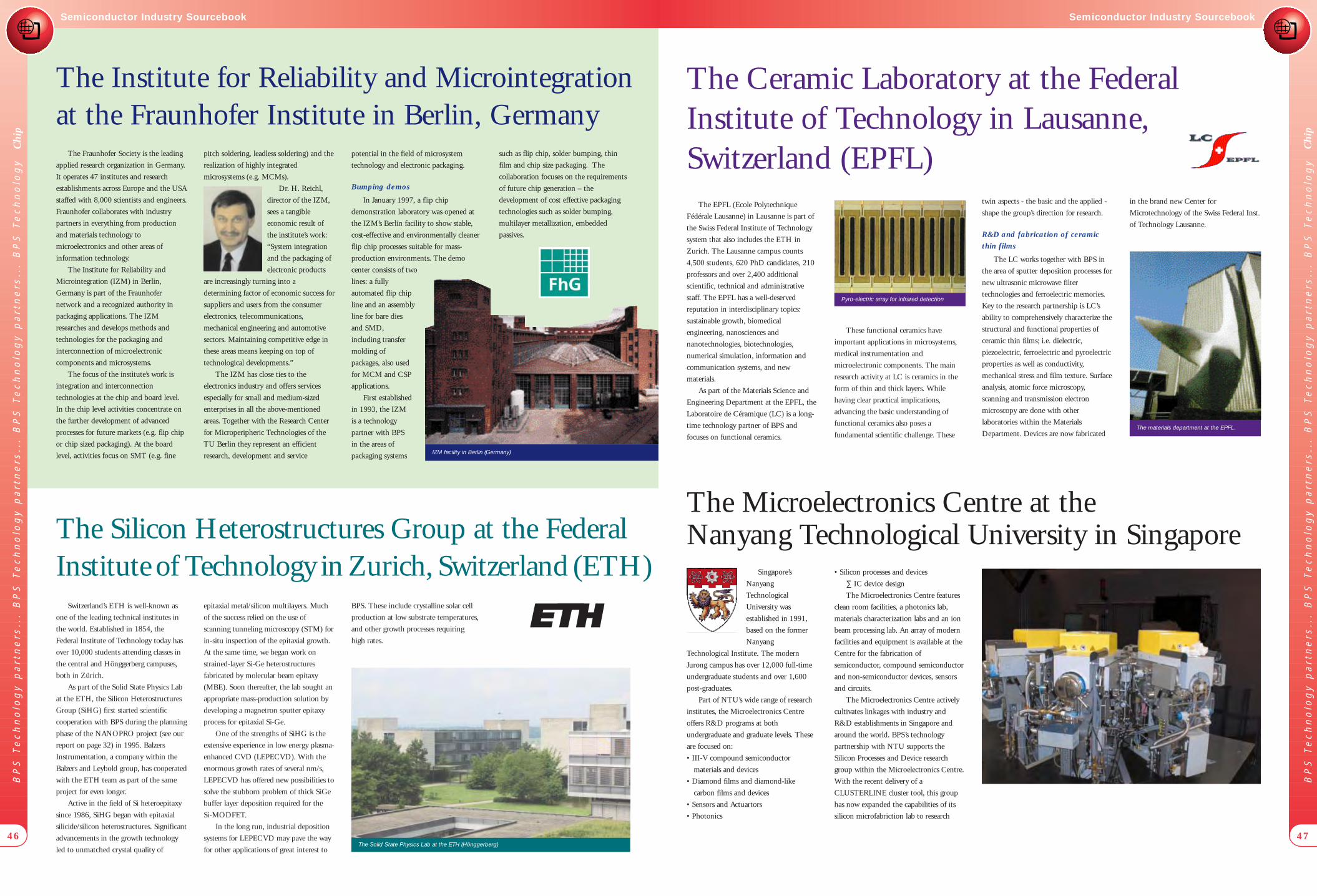
BP
S T
ec
hn
olo
gy
pa
rtn
ers
...
BP
S T
ec
hn
olo
gy
pa
rtn
ers
...
BP
S T
ec
hn
olo
gy
pa
rtn
ers
...
BP
S T
ec
hn
olo
gy
Chip
Semiconductor Industry Sourcebook
47
BP
S T
ec
hn
olo
gy
pa
rtn
ers
...
BP
S T
ec
hn
olo
gy
pa
rtn
ers
...
BP
S T
ec
hn
olo
gy
pa
rtn
ers
...
BP
S T
ec
hn
olo
gy
Chip
Semiconductor Industry Sourcebook
46
The Silicon Heterostructures Group at the FederalInstitute of Technology in Zurich, Switzerland (ETH)
Switzerland’s ETH is well-known as
one of the leading technical institutes in
the world. Established in 1854, the
Federal Institute of Technology today has
over 10,000 students attending classes in
the central and Hönggerberg campuses,
both in Zürich.
As part of the Solid State Physics Lab
at the ETH, the Silicon Heterostructures
Group (SiHG) first started scientific
cooperation with BPS during the planning
phase of the NANOPRO project (see our
report on page 32) in 1995. Balzers
Instrumentation, a company within the
Balzers and Leybold group, has cooperated
with the ETH team as part of the same
project for even longer.
Active in the field of Si heteroepitaxy
since 1986, SiHG began with epitaxial
silicide/silicon heterostructures. Significant
advancements in the growth technology
led to unmatched crystal quality of
epitaxial metal/silicon multilayers. Much
of the success relied on the use of
scanning tunneling microscopy (STM) for
in-situ inspection of the epitaxial growth.
At the same time, we began work on
strained-layer Si-Ge heterostructures
fabricated by molecular beam epitaxy
(MBE). Soon thereafter, the lab sought an
appropriate mass-production solution by
developing a magnetron sputter epitaxy
process for epitaxial Si-Ge.
One of the strengths of SiHG is the
extensive experience in low energy plasma-
enhanced CVD (LEPECVD). With the
enormous growth rates of several nm/s,
LEPECVD has offered new possibilities to
solve the stubborn problem of thick SiGe
buffer layer deposition required for the
Si-MODFET.
In the long run, industrial deposition
systems for LEPECVD may pave the way
for other applications of great interest to
The Institute for Reliability and Microintegration at the Fraunhofer Institute in Berlin, Germany
The Fraunhofer Society is the leading
applied research organization in Germany.
It operates 47 institutes and research
establishments across Europe and the USA
staffed with 8,000 scientists and engineers.
Fraunhofer collaborates with industry
partners in everything from production
and materials technology to
microelectronics and other areas of
information technology.
The Institute for Reliability and
Microintegration (IZM) in Berlin,
Germany is part of the Fraunhofer
network and a recognized authority in
packaging applications. The IZM
researches and develops methods and
technologies for the packaging and
interconnection of microelectronic
components and microsystems.
The focus of the institute’s work is
integration and interconnection
technologies at the chip and board level.
In the chip level activities concentrate on
the further development of advanced
processes for future markets (e.g. flip chip
or chip sized packaging). At the board
level, activities focus on SMT (e.g. fine
pitch soldering, leadless soldering) and the
realization of highly integrated
microsystems (e.g. MCMs).
Dr. H. Reichl,
director of the IZM,
sees a tangible
economic result of
the institute’s work:
“System integration
and the packaging of
electronic products
are increasingly turning into a
determining factor of economic success for
suppliers and users from the consumer
electronics, telecommunications,
mechanical engineering and automotive
sectors. Maintaining competitive edge in
these areas means keeping on top of
technological developments.”
The IZM has close ties to the
electronics industry and offers services
especially for small and medium-sized
enterprises in all the above-mentioned
areas. Together with the Research Center
for Microperipheric Technologies of the
TU Berlin they represent an efficient
research, development and service
potential in the field of microsystem
technology and electronic packaging.
Bumping demos
In January 1997, a flip chip
demonstration laboratory was opened at
the IZM’s Berlin facility to show stable,
cost-effective and environmentally cleaner
flip chip processes suitable for mass-
production environments. The demo
center consists of two
lines: a fully
automated flip chip
line and an assembly
line for bare dies
and SMD,
including transfer
molding of
packages, also used
for MCM and CSP
applications.
First established
in 1993, the IZM
is a technology
partner with BPS
in the areas of
packaging systems
such as flip chip, solder bumping, thin
film and chip size packaging. The
collaboration focuses on the requirements
of future chip generation – the
development of cost effective packaging
technologies such as solder bumping,
multilayer metallization, embedded
passives.
IZM facility in Berlin (Germany)
The Solid State Physics Lab at the ETH (Hönggerberg)
BPS. These include crystalline solar cell
production at low substrate temperatures,
and other growth processes requiring
high rates.
The Ceramic Laboratory at the FederalInstitute of Technology in Lausanne,Switzerland (EPFL)
The EPFL (Ecole Polytechnique
Fédérale Lausanne) in Lausanne is part of
the Swiss Federal Institute of Technology
system that also includes the ETH in
Zurich. The Lausanne campus counts
4,500 students, 620 PhD candidates, 210
professors and over 2,400 additional
scientific, technical and administrative
staff. The EPFL has a well-deserved
reputation in interdisciplinary topics:
sustainable growth, biomedical
engineering, nanosciences and
nanotechnologies, biotechnologies,
numerical simulation, information and
communication systems, and new
materials.
As part of the Materials Science and
Engineering Department at the EPFL, the
Laboratoire de Céramique (LC) is a long-
time technology partner of BPS and
focuses on functional ceramics.
These functional ceramics have
important applications in microsystems,
medical instrumentation and
microelectronic components. The main
research activity at LC is ceramics in the
form of thin and thick layers. While
having clear practical implications,
advancing the basic understanding of
functional ceramics also poses a
fundamental scientific challenge. These
Pyro-electric array for infrared detection
twin aspects - the basic and the applied -
shape the group’s direction for research.
R&D and fabrication of ceramic
thin films
The LC works together with BPS in
the area of sputter deposition processes for
new ultrasonic microwave filter
technologies and ferroelectric memories.
Key to the research partnership is LC’s
ability to comprehensively characterize the
structural and functional properties of
ceramic thin films; i.e. dielectric,
piezoelectric, ferroelectric and pyroelectric
properties as well as conductivity,
mechanical stress and film texture. Surface
analysis, atomic force microscopy,
scanning and transmission electron
microscopy are done with other
laboratories within the Materials
Department. Devices are now fabricatedThe materials department at the EPFL.
in the brand new Center for
Microtechnology of the Swiss Federal Inst.
of Technology Lausanne.
Singapore’s
Nanyang
Technological
University was
established in 1991,
based on the former
Nanyang
Technological Institute. The modern
Jurong campus has over 12,000 full-time
undergraduate students and over 1,600
post-graduates.
Part of NTU’s wide range of research
institutes, the Microelectronics Centre
offers R&D programs at both
undergraduate and graduate levels. These
are focused on:
• III-V compound semiconductor
materials and devices
• Diamond films and diamond-like
carbon films and devices
• Sensors and Actuartors
• Photonics
• Silicon processes and devices
∑ IC device design
The Microelectronics Centre features
clean room facilities, a photonics lab,
materials characterization labs and an ion
beam processing lab. An array of modern
facilities and equipment is available at the
Centre for the fabrication of
semiconductor, compound semiconductor
and non-semiconductor devices, sensors
and circuits.
The Microelectronics Centre actively
cultivates linkages with industry and
R&D establishments in Singapore and
around the world. BPS’s technology
partnership with NTU supports the
Silicon Processes and Device research
group within the Microelectronics Centre.
With the recent delivery of a
CLUSTERLINE cluster tool, this group
has now expanded the capabilities of its
silicon microfabriction lab to research
The Microelectronics Centre at theNanyang Technological University in Singapore

Semiconductor Industry Sourcebook1999
Progress of Flip Chip Technology
Taiwan is Silicon Island
Metallization, FRAMs, MRAMs
All about SiGe Technology
High-performance Failure Analysis
TECHNOLOGY CENTERS
Balzers Process SystemsP.O. Box 1000, FL-9496 Balzers, LIECHTENSTEINTel: +423 388 6388 Fax: +423 388 6500
Balzers Process Systems, GmbHSiemensstrasse 100, D-63755, Alzenau,GERMANYTel: +49 6181 34 6000 Fax: +49 6181 34 6002
Balzers Process Systems SAR & D, Display Division5 rue Léon Blum, 91120 Palaiseau, FRANCETel: +33 1 69 19 12 80 Fax: +33 1 69 32 06 60
Balzers Process Systems, Inc.25 Sagamore Park Road, Hudson, NH 03051, USATel: +1 603 594 1500 Fax: +1 603 594 1515
Balzers Process Systems, Inc.1715 Wyatt Drive, Santa Clara, CA 95054, USATel: +1 408 567 1300 Fax: +1 408 567 1313
Balzers-Hakuto Co., Ltd.Osaka Laboratory5-13, Kawagishi-cyo, Suita-city, Osaka-pref. 564-0037, JAPANTel: +81 6 4860 9120 Fax: +81 6 4860 2200
BPS-Nextral SAZAC Pré Milliet, Montbonnot BP 39, 38330 Saint-Ismier, FRANCETel: +33 476 52 3434 Fax: +33 476 52 3436
JAPAN
Balzers-Hakuto Co., Ltd.8F, Shinjuku 3-chome Building2-1, Shinjuku 3-chome, Shinjuku-ku,Tokyo 160-0022, JAPANTel: +81 3 3225 9020 Fax: +81 3 3225 9043
ASIA PACIF IC
Balzers Process Systems12/F., Belgian Bank Tower, 77 Gloucester Road, HONG KONGTel: +852 2866 2699 Fax: +852 2866 6110
Balzers Process SystemsNo. 32, Fushing Road, Hsinchu Industrial ParkHukou Hsiang, Hsinchu Hsien, Taiwan R.O.C.Tel: +886 3597 7771 Fax: +886 3598 6161
Balzers Process SystemsC.P.O. Box 709, 100-607, Seoul, KOREATel: +82 2 2270 1370 Fax: +82 2 2277 5322
Balzers Process Systems1 Tuas South Street 3, SINGAPORE 638043Tel: +65 865 1870 Fax: +65 865 1874
NORTH AMERICA
Balzers Process Systems, Inc.25 Sagamore Park Road, Hudson, NH 03051, USATel: +1 603 594 1500 Fax: +1 603 594 1515
EUROPE
Balzers Process Systems, B.V.Computerweg 7, NL-3606 AV MaarssenTHE NETHERLANDSTel: +31 3465 50 606 Fax: +31 3465 50 784
EMERGING AND OTHER MARKETS
Balzers Process SystemsP.O. Box 1000, FL-9496 Balzers, LIECHTENSTEINTel: +423 388 4706 Fax: +423 388 5402
www.bps -IT.com
Progress of Flip Chip Technology
Taiwan is Silicon Island
Metallization, FRAMs, MRAMs
All about SiGe Technology
High-performance Failure Analysis