table of contents - home - australian renewable … · web viewthe project also focused on the most...
TRANSCRIPT

Novel Texture Processes for the latest Industrial Wafer and Advanced Cell Concepts
Final report: project results and lessons learnt
Lead organisation: Suntech R&D Australia
Project commencement date: Jan 2013 Completion date: May 2015
Date published: TBD
Contact name: Nathan Chang
Email: [email protected]
1

Table of ContentsTable of Contents..................................................................................................................................2
Executive Summary...............................................................................................................................3
Project Overview...................................................................................................................................4
Project summary............................................................................................................................4
Project scope.................................................................................................................................6
Outcomes......................................................................................................................................8
Transferability..............................................................................................................................11
Conclusion and next steps...........................................................................................................12
Lessons Learnt.....................................................................................................................................13
Lessons Learnt Report: Effective R&D Collaboration...................................................................13
2

Executive SummaryThe project aimed at testing novel texturing methods for advanced cell concepts, with a view to new developments in wafer and cell processing. The strengths of the project lay in the collaboration between the equipment manufacturers (Roth& Rau), the cell manufacturer (Suntech) and the process development teams at Suntech R&D Australia and Fraunhofer ISE (FhISE). This team formed through this collaboration was uniquely placed, to develop new processes and demonstrate their application in manufacturing. We were able to source new manufacturing relevant materials, run controlled tests with novel processes alongside well established standards, and complete processing in a full manufacturing environment.
Cells process on the manufacturing lines showed improvements of the standard processes, with the average efficiency of 17.6% for the new processes being 0.5% absolute better than the standard process. The efficiency improvements achieved are small (3% relative), but the maturity of the processes and the certainty of the outcome mean that the small improvements are very relevant for manufacturing. Cost effective improvements of 3% relative per annum are typical of the incremental improvements that have taken manufacturing cell efficiencies from 14% to 19% over the last ten years.
A knowledge sharing workshop at the end of the project brought together the international project participants and allowed for public dissemination of the research outcomes.
3

Project Overview
Project summary One of the most fundamental concepts in understanding solar cell operation is that the amount of electricity generated depends on the amount of light available for conversion. Increasing the amount of light absorbed by the cell is a subject of research and development common to all solar technologies and to all levels, from blue-sky research right through to manufacturing.
This project targets manufacturing applications by testing variations on light-trapping processes for their suitability in an industrial environment. The project also focused on the most common solar cells in production – silicon wafer solar cells with screen-printed contacts, which are used in approximately 90 % of all the solar modules made world-wide.
The present industrial processes make use of two major light-trapping features:
1. An anti-reflection coating (ARC) of silicon nitride (SiNx) on the front surface of the silicon wafer and
2. Texturing (roughening) of the silicon front surface, which causes the incoming light to scatter at a shallow angle when it enters the silicon. This increases the distance that the light travels through the silicon, giving it a higher chance of absorption. A further benefit of surface texture is that it causes light reflected at the front surface to do so at an angle which may allow a second chance at transmission into the silicon. Figure 1 shows the propagation of light into encapsulated silicon via different surface textures.
Both of these features were addressed within this project. The characterisation of the ARC was improved through the development of a new in-line monitoring tool. The texture was improved through development of new processes for both standard wafers and for lower-cost alternatives.
Report title | Page 4

1. Light enters at a normal angle to the solar cell onto a planar surface. Only around 4% reflection occurs at the glass surface (not shown)
2. At the planar surface, most light is transmitted into the silicon, but a significant proportion is also reflected back out and lost from the solar cell
3. Light enters at a normal angle to the solar cell onto a highly textured surface4. Most light is refracted into the silicon, but a significant proportion is reflected downward at
a shallow angle5. The reflected light travels toward a nearby silicon surface and has a second chance at
transmission. 6. The light lost away from the cell is much lower in this scenario7. Light enters at a normal angle to the solar cell onto a mildly textured surface8. Most light is refracted into the silicon, but a significant proportion is reflected upward at a
shallow angle9. At shallow angles, the amount of light that is reflected at the glass/air interface increases
dramatically. Beyond a critical angle, 100% of light is reflected back toward the silicon.10. The reflected light has a second chance of transmission into the silicon. The light lost away
from the solar cell is much lower compared to the planar surface.
In addition to technical evaluation, cost analysis was conducted on promising technologies to test whether the processes were commercially relevant.
Report title | Page 5
Figure 1: Different scattering paths for light into encapsulated cells with different surface textures

Project scopeThe project aimed at testing novel texturing methods for advanced cell concepts, such as all-rear-contact cells and thin wafers. The focus shifted early to processes which could be implemented quickly into manufacturing lines to reduce cost and/or increase efficiency in the increasingly competitive PV module market.
To this end, the following streams were pursued:
1. Plasma texturing (reactive ion etching)2. Diamond-Wire sawing of wafers3. Development of characterisation tools4. Manufacturing cost analysis
Texturing
The state-of-the-art texturing processes use wet-chemical etches to attack the silicon surface and leave it in a roughened state. For multicrystalline wafers, this is done with a combination of acids, which etch the silicon in a way which is dependent upon the initial surface roughness. For monocrystalline wafers, this is done with an alkaline solution, which etches the silicon according to its crystal structure, leaving a pyramidal texture which is very effective at light-trapping. The dependence upon crystal structure means this etch is not appropriate for multicrystalline wafers.
An alternative texturing method is the use of reactive ion etching, or ‘plasma’ texturing. This method etches the surface in a somewhat random manner, mostly independently of initial surface roughness or crystal structure. It therefore allows for greater uniformity and improved light-trapping on multicrystalline wafers.
Wafer sawing
Silicon is first formed into high quality bricks or ingots which need to be sawn into the thin wafers used in solar cells. The state-of-the-art sawing process uses a slurry of silicon carbide particles which are rubbed against the silicon by many parallel wires in order to saw through the brick. A lower-cost alternative is ‘diamond-wire’ sawing, which uses many parallel diamond coated wires. This removes the need for the slurry, allows for thinner wafer sawing and reduces the amount of silicon which is lost in the process. However, the resulting silicon surface is not sufficiently uniform to allow the state-of-the-art acid-etch texturing processes to be effective. New texture processes, including plasma texturing were tested as alternatives.
Silicon nitride characterisation
The SiN optical thickness and uniformity is crucial both for cell performance and appearance. At present, assessment is done either by eye, which is unreliable and inconsistent, or by use of an ellipsometer, which requires wafers to be taken off-line and measured several times and is slow and labour intensive.
This project included development of a faster, automated, in-line tool to replace the existing characterisation methods.
Report title | Page 6

Both multicrystalline and monocrystalline wafers were used in development, although with an increasing emphasis on multicrystalline as this type asserted dominance in the manufacturing lines.
The scope of process validation was primarily to show cost savings or efficiency improvements on pilot lines sufficiently reflecting the industrial environment, with stretch goals of integrating the processes on real manufacturing lines.
Manufacturing Cost
Manufacturing cost analysis considered:
1. Estimates of the change in manufacturing cost per module produced. This included the cost saving of using diamond wire sawn wafers as well as the cost increase of the new texturing processes.
2. The additional effect of efficiency improvements. Higher efficiency means more power (Watts) per module, which means a lower manufacturing cost per Watt.
Report title | Page 7

OutcomesPlasma textured vs wet-chemically textured wafers
During this project the plasma texturing process was developed such that solar cell conversion efficiency was increased by 3 % relative to the state-of-the-art acid etch process for multicrystalline wafers. This was achieved using a Roth & Rau MAiATex tool with a new texturing process. Figure 2 shows that the increased performance was primarily due to an increase in short-circuit current (ISC), which is the expected result of an improved light-trapping texture.
Diamond-wire sawn wafers
Diamond-wire sawing of wafers offers a higher yield, but leaves the surface with additional features that require innovation in the texturing process. However the wire leaves deep trenches parallel to the sawing direction, as shown in the comparison of the surfaces of diamond wire sawn wafer and the standard slurry sawn in Figure 3. Since the state-of-the-art acid-etch texturing process requires a uniform surface to be effective, it is not compatible with diamond-wire sawn wafers.
In this project we use plasma texturing which works independently of wafer surface and an acid-etch process tested as an alternative etch chemistry. In each case these methods resulted in wafer reflectivity for diamond-wire-sawn wafers which was equivalent to the corresponding process using state-of-the art slurry sawing, as shown in Figure 4. Figure 4 also shows the improvement in reflectivity using plasma texturing compared to wet-texturing for both wafer types.
Report title | Page 8
Figure 2: Efficiency and Short Circuit Current values for four groups of novel plasma textured cells (PT) and one group of wet textured cells (WT).The relative improvement for both Eff and ISC is 3 % with an absolute improvement of 0.5 % and 0.3 A respectively

Report title | Page 9
Figure 3: Diamond-wire sawn (left) and slurry-sawn (right) wafers
Figure 4: Reflectivity and estimate short-circuit current density (JSC) loss using two different plasma texture processes (Partner A and Partner B) and an alternative acid-etch chemistry (Partner C). SWS = state-of-the-art slurry wire sawing; DWS = new alternative diamond-wire sawing

Silicon Nitride Scanner (SiNS)
One of the characterisation tools developed within this project allowed for wafers to be rapidly scanned in-line after the deposition of the Silicon Nitride (SiN) anti-reflection coating.
The Silicon Nitride Scanner (SiNS) tool can provide more information faster and with no manual intervention than is possible with competing process control tools.
The SiNS tool finds the minimum wavelength at over 1000 points across the wafer area in approximately one second, allowing optical thickness and uniformity to be recorded and monitored automatically. The correlation between wafer colour (which is dependent upon SiN properties) and the minimum wavelength of the reflectance curve is shown in Figure 5.
Cost Analysis
Analysis showed that the plasma texturing process on multicrystalline wafers would contribute to an improvement in manufacturing costs of around A$0.04 / W, assuming that the efficiency gains of this process are maintained.
Report title | Page 10
Figure 5: Wafer colour after Silicon Nitride deposition matched to minimum wavelength of reflectance curve

TransferabilityPlasma texturing
The use of plasma textured wafers was tested on a Suntech production line in the early stages of the project. Despite texture processes which were not fully developed and downstream processing which was not tailored to the different texture, the best cells performed to within ~0.3 % absolute efficiency of the control group. This suggests that there are no significant barriers to the use of this process in production. With optimisation of the downstream processes, it is considered very likely that the 0.5 % absolute efficiency increase shown in Figure 2 would be achieved in production. Further, with the greater statistical power afforded by large scale manufacturing, it is likely that the process could be fine-tuned to provide an even greater benefit.
Diamond-wire sawing
Diamond-wire sawn multicrystalline wafers have yet to pass every test of compatibility with manufacturing. Despite the equivalent optical performance shown in Figure 3, pilot line efficiencies lagged those of the state-of-the-art process by at least 0.6 % absolute. Issues which still need to be resolved include material quality and contact printing. Nevertheless, these wafers have also been tested on a Suntech production line, with best cells achieving over 17 % efficiency. This suggests that compatibility with these production lines is likely when the performance has been improved.
Silicon Nitride Scanner (SiNS)
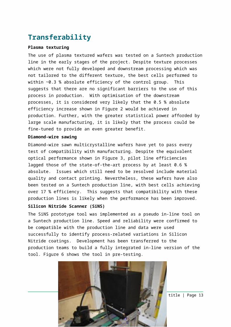
The SiNS prototype tool was implemented as a pseudo in-line tool on a Suntech production line. Speed and reliability were confirmed to be compatible with the production line and data were used successfully to identify process-related variations in Silicon Nitride coatings. Development has been transferred to the production teams to build a fully integrated in-line version of the tool. Figure 6 shows the tool in pre-testing.
Report title | Page 11
Figure 6: Silicon Nitride Scanner prototype tool

Conclusion and next stepsThe Advanced Texture project looked at new texture processes as improvements to those used in standard cell manufacturing and to extend the standard cell manufacturing processes to include new techniques in wafering. The project brought together Australian and German partners in research and manufacturing to test new approaches in manufacturing on the manufacturing lines in China.
In this project,
Novel plasma texturing was shown to result in efficiencies in manufacturing production that are comparable with cells produced using standard cell line processes on slurry sawn wafers.
Novel plasma texturing was applied to new methods for wafer production with the aim of delivering a new wafering + texturing technology that will result in lower manufacturing cost through increased yield. Progress was made in demonstrating the equivalence in performance with the new processes.
The characterisation of the anti-reflection process was improved through the development of a new in-line monitoring tool.
Significant benefit from the project came from the international collaboration and the engagement of equipment manufacturers with research on manufacturing lines.
A knowledge sharing workshop at the end of the project brought together the international project participants and allowed for public dissemination of the research outcomes.
This work will continue at the German Partners. They are seeking to continue to engage with new partners at University of New South Wales (Dr A Lennon) and with Suntech and other equipment manufacturers. Next steps would include:
Ongoing lab based R&D to demonstrate efficiency improvement and refine manufacturing cost estimates.
Once sufficient progress has been made, this may justify the cost of a Pilot Line demonstration. This pilot line would demonstrate yield and efficiency improvement and validate the manufacturing cost estimates.
Once the pilot line demonstration is successful, this may justify the cost of implementing this in production.
Report title | Page 12
Lessons Learnt
Lessons Learnt Report: Effective R&D Collaboration Project Name: 3-GER003 Novel Texture Processes for the Latest Industrial Wafer and Advanced Cell Concepts
Knowledge Category: Technical
<Choose an Item>Knowledge Type:
Technology
Technology Type: Solar PV
<Choose an item>State/Territory:
NSW
Key learningIt is highly beneficial to bring together institutions, solar module manufacturers and manufacturing tool suppliers in a collaborative research project. Ensuring good information sharing and taking advantage of synergies increase technology progress and knowledge development.
Implications for future projectsA collaborative project like this one can be a very helpful in bringing groups together and speeding up technical developments. These collaborations will benefit from open sharing of information in both planning and analysing experimental work. Some effort should be put into planning how best to use the strengths of each organisation to gain maximum benefit from the project.
Background
Objectives or project requirements
This project aimed to identify and test new texturing processes for solar cell fabrication.
Process undertaken
This project brought together the R&D teams from a PV Module manufacturer (Suntech R&D Australia), a production tool supplier (Roth & Rau) and a research institute (Fraunhofer ISE). There were a number of processes that benefits greatly from this collaboration.
Information sharing during planning – each partner brought previous learning to the project regarding what processes worked well, what areas needed work. This allowed the project experimental runs to avoid unnecessary replication of previous work, thus making the project more effective.
Information sharing and analysis of results – sharing the experimental run results with all partners allowed better understanding and analysis of the results. For example, unexpected performance deficits could often be explained by one partner and thus avoiding false
13

conclusions. This sharing also allowed each party to improve their part of the process for the next round of work together.
Other synergies – each partner brought its’ own capabilities to the project. This included different expertise, equipment, intellectual property and perspective. Early in the project the partners worked out how to best take advantage of these differences to gain maximum benefit to the project.
All of this was aided by having in-person meetings between the project partners. Although this involved significant travel expense (with partners based in Australia and Germany), the benefits in effective information sharing and planning were very significant.
Report title | Page 14