table of contents...full scale illuminated as can be seen in the left column, which shows a full...
TRANSCRIPT


2
TABLE OF CONTENTS
Welcome . . . . . . . . . . . . . . . . . . . . . . . . . . . . . . . . . . . . . . . . . . pg 03
Dynamic Range, What Is It Good for Anyway? . . . . . . . . . . . . pg 04
Why Is Binning Different in CMOS Image Sensors Compared to CCD Image Sensors . . . . . . . . . . . . . . pg 08
Are Larger Pixels Always More Sensitive? . . . . . . . . . . . . . . . pg 12
What Is All the Hype About Resolution and Mega Pixels Anyway? . . . . . . . . . . . . . . . . . . . . . . . . . . . . pg 19
Lab Obstacle Run . . . . . . . . . . . . . . . . . . . . . . . . . . . . . . . . . . . pg 24
Is It True That Cooled Cameras Are More Sensitive Than Non-Cooled Cameras . . . . . . . . . . . . . . pg 26
DNA-Paint: a Super-Resolution Microscopy Technique . . . . . pg 29
Standards Always Sound Impressive, but Is There Any Benefit for Me As an sCMOS Camera User? . . . . . . . . . . . . . . . . . . . . . . . . . . . . . . . pg 31
Why Is a Backside Illuminated Sensor More Sensitive Than a Front Side Illuminated? . . . . . . . . . . . . pg 34
Why Does High-Resolution Inspection of Food Products Matter? . . . . . . . . . . . . . . . . . . . . . . . . . . . . pg 37
What Are All the Discussions About Global vs . Rolling Shutter? . . . . . . . . . . . . . . . . . . . . . . pg 39
Why Are There Special Interfaces for the Transmission of Image Data? . . . . . . . . . . . . . . . . . . . pg 51

3
WELCOME
In the years since their first appearance in 2010, scientific cameras based on scientific CMOS image sensors have had a large impact on numerous new technologies and methods in science due to their ideal combination of low readout noise, high quantum efficiency and high frame rates.
Improvements in wafer fabrication as well as new sensor design methodol-ogies have enabled significant improvements in sCMOS image sensors in the last couple of years. The wafer scale backside thinning process is now a standard manufacturing process due to the huge investments from the cell phone industry. The newest sCMOS are now available in backside thinned versions. Scientific camera design methodologies have evolved too. Even the first passively cooled sCMOS cameras are available today.
This is an exciting technological race and you, as the user, will benefit further even more in the years to come. However, there are some common and some peculiar characteristics about the sCMOS sensor and its behavior, which will not change and can raise some questions.
Most prominently, the difference between global shutter vs rolling shutter. We will uncover this topic on page 39. Why is binning different in sCMOS image sensors compared to CCD image sensors? Start reading on page 8. Learn about the benefits of test standards for cameras on page 31. The question about the sensitivity of cooled vs. uncooled cameras may surprise you start-ing on page 26.
This book might not cover every detail you always wanted to know about sCMOS cameras, but it might provide something you were afraid to ask. This is your chance.
I trust you will find this information helpful and fun to read!
Dr. Emil Ott
CEO, PCO AG

4
DYNAMIC RANGE,WHAT IS IT GOODFOR ANYWAY?
The “dynamic” or “dynamic range” of an image sensor or a camera system characterizes the ability of a cam-era system to measure and distinguish different levels of light. This characterization corresponds with the maxi-mum contrast that can be successfully attained in a single image. The correct technical terminology is “intra-scene dynamic range”, but generally camera manufacturers just refer to the “dynamic” or the “dynamic range” in their technical data sheets and marketing materials. In the photography � eld, dynamic range is analogous to the contrast range. However, many camera manufacturers de� ne dynamic range from various perspectives. There-fore, a distinction must be made between the various terminologies; “dynamic range of an sCMOS, CMOS or CCD image sensor”, “dynamic range of an analog-to-dig-ital-conversion”, “usable dynamic range” and “maximum dynamic range or maximum SNR”.
Bene� t and Relevancefor a Camera User
One may ask, ‘What is the bene� t of a large dynamic or dynamic range of a camera?’ The short answer is more information. Since many displays and TV screens exhibit an 8-bit dynamic range, they mimic the untrained eye (able to distinguish only ~256 light levels between black and white). A radiologist, however, is trained to see more, and may need a screen displaying 10 bits. Yet for the general public, 8 bits may be more than good enough (8- to 10-bit smartphone cameras tend to deliver seemingly high quality and colorful pictures after all). Then why may we need more information?
A higher intra-scene dynamic range corresponds to a larger amount of light levels which can be detected and distinguished. How can this be perceived or used? Let us take the 4 images in � gure 1 as an example. The
extracts in the four columns have been generated from the same 16 bit raw image taken with a pco.edge 5.5 color sCMOS camera. The original image was exposed such that the bright lights of the supermarket at night did not overexpose and can be seen from the full range conversion from 16 to 8 bit. Therefore, the full amount of information is present in the raw data but cannot be observed in this version of the image. From left to right, the conversion range is minimized, revealing from col-umn to column more details (thus, more information) in the darker areas of the image. Finally, the right column depicts the conversion down to the low light range, gen-
Figure 1: Four extracts of the same night image, which was taken one evening outside the lab of a supermarket in Kelheim using a pco.edge 5.5 color sCMOS camera system. Each image demonstrates how the 16 bit image was scaled to the 8 bit world of the print or the screen, but all versions have been created from the same raw data � le. The image on the left side shows a full scale conversion (value 65536 (16 bit max) -> value 256 (8 bit max) and value 0 (16 bit) -> value 0 (8 bit)), while image on the right shows a low scale conversion (value 1024 (16 bit low) -> value 256 (8 bit max) and value 0 (16 bit) -> value 0 (8 bit)). The other images show different conversions in between.
erating “overexposed” areas (due to the conversion), but also allowing to distinguish tiny details formerly hidden in the shadows. Scaling between bit depths is a handy tool to observe more information due to a higher dynam-ic range. And for some applications, like a high quality 3D measurement, if non-cooperative (highly re� ecting) surfaces are involved, it is prerequisite to scale appropri-ately to discern the relevant contrast.
output photo in an optimum way that structures can be seen both in the shadows and in the light, provided that the camera has a large enough dynamic range.
Calculating the Dynamic Rangeof a Digital Image Sensor
The dynamic range (dynimsens) is de� ned as the ratio of the maximum possible signal (which is in most cases identi-cal or near to the “full well capacity” describing the max-imum number of charge carriers a pixel could generate and collect), versus the total readout noise signal1 (in the dark). The data is either dimensionless and expressed as a ratio or expressed in decibels [dB]:
dynimsens = fullwell capacity [e⁻]
readout noise [e⁻]
dynimsens = 20 ∙ log fullwell capacity [e⁻]
readout noise [e⁻] [dB]
Figure 2: Four extracts of the same � uorescent image of a Calcium indicator in neurons, which was taken with a pco.edge 5.5 sCMOS camera system. The total image was not full scale illuminated as can be seen in the left column, which shows a full scale conversion (value 65536 (16 bit max) -> value 256 (8 bit max) and value 0 (16 bit) -> value 0 (8 bit)). The second of the left images shows a conversion which scales the maximum signal in the image to the maximum of 8 bit, the � uorescence can be seen, but some of the con-nections remain in the dark. The third image has a low scale conversion, now the connections can be well identi� ed but some areas seem overexposed and don’t show structural information therefore. The � nal image applies a non-linear conversion, which allows to display most of the structural information in the 8 bit world of the screen or the print.
Let us take a look at another example. The original raw data of a � uorescent calcium indicator in neurons was taken with a pco.edge 5.5 sCMOS camera. Here, the image was not fully exposed, as seen from the far left col-umn showing a full scale conversion, resulting in a dark image. The next column was converted to the maximum signal in the image, showing a few visible structures, but the connections between the neurons can hardly be seen. When the conversion is lowered, in the third col-umn, the connections can be seen but the neurons are “overexposed”. To overcome this in the fourth column a non-linear conversion is shown, which allows the analysis of the structure.
In commercial photography applications, a higher dy-namic range allows for the adjustment of the 8-bit � nal
ParameterSony
ICX285 CCD
Sony IMX174
CMOSIS CMV4000
BAECIS2020A
Fullwellcapacity [e-]
18000 30000 13500 30000
Readout Noise [e-]
5 6 13.5 0.8
Dynamic range
3600 : 1 5000 : 1 1000 : 1 37500 : 1
Dynamic range [dB]
71.1 74.0 60.0 91.5
Table 1: dynamic range data of common image sensors
When the full dynamic range of the image sensor is available to the user, then any additional application of gain, which makes the image brighter, is not providing any additional information or bene� t to the user. Quite the opposite is the case. A gain would reduce the us-able dynamic range, since the change from one light level to the next would just cause a larger step in the digital signal and result in saturation of the image val-ues at a much lower light level. Therefore, the use of an additional gain only helps if the dynamic range of the A/D-converter is smaller than the dynamic range of the image sensor. For example, the IMX174 would bene� t from a 13 bit A/D conversion but the image sensor is
DYNAMIC RANGE

5
DYNAMIC RANGE,WHAT IS IT GOODFOR ANYWAY?
The “dynamic” or “dynamic range” of an image sensor or a camera system characterizes the ability of a cam-era system to measure and distinguish different levels of light. This characterization corresponds with the maxi-mum contrast that can be successfully attained in a single image. The correct technical terminology is “intra-scene dynamic range”, but generally camera manufacturers just refer to the “dynamic” or the “dynamic range” in their technical data sheets and marketing materials. In the photography � eld, dynamic range is analogous to the contrast range. However, many camera manufacturers de� ne dynamic range from various perspectives. There-fore, a distinction must be made between the various terminologies; “dynamic range of an sCMOS, CMOS or CCD image sensor”, “dynamic range of an analog-to-dig-ital-conversion”, “usable dynamic range” and “maximum dynamic range or maximum SNR”.
Bene� t and Relevancefor a Camera User
One may ask, ‘What is the bene� t of a large dynamic or dynamic range of a camera?’ The short answer is more information. Since many displays and TV screens exhibit an 8-bit dynamic range, they mimic the untrained eye (able to distinguish only ~256 light levels between black and white). A radiologist, however, is trained to see more, and may need a screen displaying 10 bits. Yet for the general public, 8 bits may be more than good enough (8- to 10-bit smartphone cameras tend to deliver seemingly high quality and colorful pictures after all). Then why may we need more information?
A higher intra-scene dynamic range corresponds to a larger amount of light levels which can be detected and distinguished. How can this be perceived or used? Let us take the 4 images in � gure 1 as an example. The
extracts in the four columns have been generated from the same 16 bit raw image taken with a pco.edge 5.5 color sCMOS camera. The original image was exposed such that the bright lights of the supermarket at night did not overexpose and can be seen from the full range conversion from 16 to 8 bit. Therefore, the full amount of information is present in the raw data but cannot be observed in this version of the image. From left to right, the conversion range is minimized, revealing from col-umn to column more details (thus, more information) in the darker areas of the image. Finally, the right column depicts the conversion down to the low light range, gen-
Figure 1: Four extracts of the same night image, which was taken one evening outside the lab of a supermarket in Kelheim using a pco.edge 5.5 color sCMOS camera system. Each image demonstrates how the 16 bit image was scaled to the 8 bit world of the print or the screen, but all versions have been created from the same raw data � le. The image on the left side shows a full scale conversion (value 65536 (16 bit max) -> value 256 (8 bit max) and value 0 (16 bit) -> value 0 (8 bit)), while image on the right shows a low scale conversion (value 1024 (16 bit low) -> value 256 (8 bit max) and value 0 (16 bit) -> value 0 (8 bit)). The other images show different conversions in between.
erating “overexposed” areas (due to the conversion), but also allowing to distinguish tiny details formerly hidden in the shadows. Scaling between bit depths is a handy tool to observe more information due to a higher dynam-ic range. And for some applications, like a high quality 3D measurement, if non-cooperative (highly re� ecting) surfaces are involved, it is prerequisite to scale appropri-ately to discern the relevant contrast.
output photo in an optimum way that structures can be seen both in the shadows and in the light, provided that the camera has a large enough dynamic range.
Calculating the Dynamic Rangeof a Digital Image Sensor
The dynamic range (dynimsens) is de� ned as the ratio of the maximum possible signal (which is in most cases identi-cal or near to the “full well capacity” describing the max-imum number of charge carriers a pixel could generate and collect), versus the total readout noise signal1 (in the dark). The data is either dimensionless and expressed as a ratio or expressed in decibels [dB]:
dynimsens = fullwell capacity [e⁻]
readout noise [e⁻]
dynimsens = 20 ∙ log fullwell capacity [e⁻]
readout noise [e⁻] [dB]
Figure 2: Four extracts of the same � uorescent image of a Calcium indicator in neurons, which was taken with a pco.edge 5.5 sCMOS camera system. The total image was not full scale illuminated as can be seen in the left column, which shows a full scale conversion (value 65536 (16 bit max) -> value 256 (8 bit max) and value 0 (16 bit) -> value 0 (8 bit)). The second of the left images shows a conversion which scales the maximum signal in the image to the maximum of 8 bit, the � uorescence can be seen, but some of the con-nections remain in the dark. The third image has a low scale conversion, now the connections can be well identi� ed but some areas seem overexposed and don’t show structural information therefore. The � nal image applies a non-linear conversion, which allows to display most of the structural information in the 8 bit world of the screen or the print.
Let us take a look at another example. The original raw data of a � uorescent calcium indicator in neurons was taken with a pco.edge 5.5 sCMOS camera. Here, the image was not fully exposed, as seen from the far left col-umn showing a full scale conversion, resulting in a dark image. The next column was converted to the maximum signal in the image, showing a few visible structures, but the connections between the neurons can hardly be seen. When the conversion is lowered, in the third col-umn, the connections can be seen but the neurons are “overexposed”. To overcome this in the fourth column a non-linear conversion is shown, which allows the analysis of the structure.
In commercial photography applications, a higher dy-namic range allows for the adjustment of the 8-bit � nal
ParameterSony
ICX285 CCD
Sony IMX174
CMOSIS CMV4000
BAECIS2020A
Fullwellcapacity [e-]
18000 30000 13500 30000
Readout Noise [e-]
5 6 13.5 0.8
Dynamic range
3600 : 1 5000 : 1 1000 : 1 37500 : 1
Dynamic range [dB]
71.1 74.0 60.0 91.5
Table 1: dynamic range data of common image sensors
When the full dynamic range of the image sensor is available to the user, then any additional application of gain, which makes the image brighter, is not providing any additional information or bene� t to the user. Quite the opposite is the case. A gain would reduce the us-able dynamic range, since the change from one light level to the next would just cause a larger step in the digital signal and result in saturation of the image val-ues at a much lower light level. Therefore, the use of an additional gain only helps if the dynamic range of the A/D-converter is smaller than the dynamic range of the image sensor. For example, the IMX174 would bene� t from a 13 bit A/D conversion but the image sensor is
DYNAMIC RANGE

6
just supplied with a 12 bit output. In this case, the ad-justment of the gain allows the user to position the A/D range in a way such that it is either optimum for the lower or the higher end of the range of light levels. The CMV4000 allows the user to read out either 8 – 10 – 12 bit values with an impact on frame rate and amount of data. Clearly, the 12 bit readout for a 10 bit dynamic range image sensor does give higher resolved noise values, but does not give more information, since the dynamic range is just about 10 bit.
Digitization or A/D ConversionDynamic Range
Generated charge carriers are usually converted into voltage signals through an optimized readout circuit (for CCD image sensors at the end of the readout regis-ters and for CMOS image sensors in each pixel and at the end of the columns). These signals are ampli-fi ed and fi nally digitized by an analog-to-digital (A/D) converter. Thus, the light signals (photons) are convert-ed into digital values. The analog-to-digital converters have their own given resolution or dynamic range, that in most cases is presented as a power of the base 2, (2x). This means that an 8 bit resolution corresponds to 256 steps or levels, which can be used to subdivide or convert the full scale voltage signal.
Camera manufacturers usually optimize a combina-tion of the dynamic range of the corresponding image sensor, gain and conversion factor (defi ned as aver-age conversion ratio that takes x electrons to generate one count or digital number in the image) to match the dynamic range of the image sensor with the dynamic range of the A/D converter. In case the dynamic range value of the A/D converter is larger than the dynamic range of the image sensor (see 12 bit readout data of the CMV4000 in table1) often the camera manufactur-
ers tend to give the A/D converter value as dynamic range value in their technical data sheets, which can be misleading. Therefore it is good to keep in mind that the dynamic range of the digitization is not necessarily identical to the usable dynamic range.
The resolutions above directly correspond to the theoretical maximum limit of the converter devices. Analog-to-digital converters have an average conversion uncertainty of 0.4 - 0.7 bit, which reduces the resolution for practical appli-cations by ~1 bit. If the camera system is not limited in its dynamic range by A/D converter discrepancies, it is useful to infl ate the A/D converter resolution by 1 or 2 bits.
Maximum SNR or Dynamic of a Pixel
Sometimes people analyze the technical data of an im-age sensor and look to the capabilities of a single pixel. For the image quality and the performance of each pixel the critical parameter is the signal-to-noise-ratio (SNR), because the larger it is the better the image quality is.
Resolution [bit] x => 2x
Dynamic rangeA/D conversion[digitzing steps]
Dynamic range A/D conversion [dB]
8 256 48.2
10 1024 60.2
12 4096 72.3
14 16384 84.3
16 65536 96.3
Table 2: dynamic range of binary resolution
Figure 3: Four versions of a � uorescence image of a conval-laria slice with different signal-to-noise-ratio settings (SNR = 15 – 10 – 5 – 2) to illustrate the in� uence on image quality. The white framed images within the image show a zoomed part of the total image to overcome the “low pass” � lter effect if the total image is reproduced at a lower resolution.
DYNAMIC RANGE
In fi gure 3, the impact of different signal-to-noise-ratios is shown ranging from 15 – 10 – 5 – 2. Since the eye is very sensitive and adept at resolving structures, each image has the same structure zoomed in and blown up. The SNR = 2 image results in a convallaria structure the
eye and our brain are still able to resolve, but would be near impossible to determine the structures by means of image processing, due to the higher noise levels.
In the low light range, the SNR is strongly infl uenced by the total readout noise of the image sensor and the cam-era, due to known limitations based in physics. Therefore, if an experiment is anticipated to have very low signal, the more important it is to have extremely low readout noise. The larger the light signal becomes, the more the readout noise of the camera becomes negligible and the noise behavior of the light signal itself becomes dominant. The photon or shot noise cannot be changed since it is related to the nature and physics of light. It corresponds to the square root of the number of photons. This in turn means that the SNR as ratio of the number of photons divided by the square root of the number of photons itself fi nally corresponds to the square root of the number of photons.
SNRlarge signal = number of photons
number of photons = number of photons
With this defi nition, the SNRmax should be maximized, of which there are two basic avenues. Either the image sensor is capable of collecting as much light as possible (a large full well e- capacity) or it is insensitive (large levels of light are collected to generate a high quality image).
Furthermore, the maximum SNR in each pixel corre-sponds to the square root of the fullwell capacity of the pixel (see table 1):
ICX285 SNRmax = 134.1
IMX174 SNRmax = 173.2
CMV4000 SNRmax = 116.2
CIS2020A SNRmax = 173.2
This is sometimes taken as maximum “dynamic range” of a pixel, which is a lot smaller than the intra-scene dy-namic range or dynamic range of the image sensor. But there are only few applications which suffer from the re-quirement to achieve the maximum SNR because they have too much light.
END NOTES
1 The dark current contribution has been neglected for the considerations,because in most applications it is only relevant for very long exposure times.
DYNAMIC RANGE

7
just supplied with a 12 bit output. In this case, the ad-justment of the gain allows the user to position the A/D range in a way such that it is either optimum for the lower or the higher end of the range of light levels. The CMV4000 allows the user to read out either 8 – 10 – 12 bit values with an impact on frame rate and amount of data. Clearly, the 12 bit readout for a 10 bit dynamic range image sensor does give higher resolved noise values, but does not give more information, since the dynamic range is just about 10 bit.
Digitization or A/D ConversionDynamic Range
Generated charge carriers are usually converted into voltage signals through an optimized readout circuit (for CCD image sensors at the end of the readout regis-ters and for CMOS image sensors in each pixel and at the end of the columns). These signals are ampli-fi ed and fi nally digitized by an analog-to-digital (A/D) converter. Thus, the light signals (photons) are convert-ed into digital values. The analog-to-digital converters have their own given resolution or dynamic range, that in most cases is presented as a power of the base 2, (2x). This means that an 8 bit resolution corresponds to 256 steps or levels, which can be used to subdivide or convert the full scale voltage signal.
Camera manufacturers usually optimize a combina-tion of the dynamic range of the corresponding image sensor, gain and conversion factor (defi ned as aver-age conversion ratio that takes x electrons to generate one count or digital number in the image) to match the dynamic range of the image sensor with the dynamic range of the A/D converter. In case the dynamic range value of the A/D converter is larger than the dynamic range of the image sensor (see 12 bit readout data of the CMV4000 in table1) often the camera manufactur-
ers tend to give the A/D converter value as dynamic range value in their technical data sheets, which can be misleading. Therefore it is good to keep in mind that the dynamic range of the digitization is not necessarily identical to the usable dynamic range.
The resolutions above directly correspond to the theoretical maximum limit of the converter devices. Analog-to-digital converters have an average conversion uncertainty of 0.4 - 0.7 bit, which reduces the resolution for practical appli-cations by ~1 bit. If the camera system is not limited in its dynamic range by A/D converter discrepancies, it is useful to infl ate the A/D converter resolution by 1 or 2 bits.
Maximum SNR or Dynamic of a Pixel
Sometimes people analyze the technical data of an im-age sensor and look to the capabilities of a single pixel. For the image quality and the performance of each pixel the critical parameter is the signal-to-noise-ratio (SNR), because the larger it is the better the image quality is.
Resolution [bit] x => 2x
Dynamic rangeA/D conversion[digitzing steps]
Dynamic range A/D conversion [dB]
8 256 48.2
10 1024 60.2
12 4096 72.3
14 16384 84.3
16 65536 96.3
Table 2: dynamic range of binary resolution
Figure 3: Four versions of a � uorescence image of a conval-laria slice with different signal-to-noise-ratio settings (SNR = 15 – 10 – 5 – 2) to illustrate the in� uence on image quality. The white framed images within the image show a zoomed part of the total image to overcome the “low pass” � lter effect if the total image is reproduced at a lower resolution.
DYNAMIC RANGE
In fi gure 3, the impact of different signal-to-noise-ratios is shown ranging from 15 – 10 – 5 – 2. Since the eye is very sensitive and adept at resolving structures, each image has the same structure zoomed in and blown up. The SNR = 2 image results in a convallaria structure the
eye and our brain are still able to resolve, but would be near impossible to determine the structures by means of image processing, due to the higher noise levels.
In the low light range, the SNR is strongly infl uenced by the total readout noise of the image sensor and the cam-era, due to known limitations based in physics. Therefore, if an experiment is anticipated to have very low signal, the more important it is to have extremely low readout noise. The larger the light signal becomes, the more the readout noise of the camera becomes negligible and the noise behavior of the light signal itself becomes dominant. The photon or shot noise cannot be changed since it is related to the nature and physics of light. It corresponds to the square root of the number of photons. This in turn means that the SNR as ratio of the number of photons divided by the square root of the number of photons itself fi nally corresponds to the square root of the number of photons.
SNRlarge signal = number of photons
number of photons = number of photons
With this defi nition, the SNRmax should be maximized, of which there are two basic avenues. Either the image sensor is capable of collecting as much light as possible (a large full well e- capacity) or it is insensitive (large levels of light are collected to generate a high quality image).
Furthermore, the maximum SNR in each pixel corre-sponds to the square root of the fullwell capacity of the pixel (see table 1):
ICX285 SNRmax = 134.1
IMX174 SNRmax = 173.2
CMV4000 SNRmax = 116.2
CIS2020A SNRmax = 173.2
This is sometimes taken as maximum “dynamic range” of a pixel, which is a lot smaller than the intra-scene dy-namic range or dynamic range of the image sensor. But there are only few applications which suffer from the re-quirement to achieve the maximum SNR because they have too much light.
END NOTES
1 The dark current contribution has been neglected for the considerations,because in most applications it is only relevant for very long exposure times.
DYNAMIC RANGE

8
WHY IS BINNINGDIFFERENT IN CMOSIMAGE SENSORS COMPAREDTO CCD IMAGE SENSORS?
The fundamental reason for the difference is the difference in technology and how the corresponding signals, the light induced charge carriers are treated and processed. Further, due to the historical pathway, at fi rst, “binning” was introduced in CCD image sensors. CCD image sen-sors allow for lossless transport of charge carrier pack-ages through their storage locations called registers, and they enable a lossless accumulation or summation of the charge carrier packages. Both of these features enabled “binning” to improve the signal-to-noise ratio.
Binning in CCD Image Sensors
The combination of the charge carrier content (generated by the impinging light signal) of two or more pixels of a CCD image sensor to form a new so-called super pix-el prior to readout and digitizing is called “binning.” This results in a summation of the generated charge carriers
from the single pixels, and it is usually done in the hor-izontal readout registers. The biggest advantage is the improvement of the signal-to-noise-ratio (SNR). Since the signal is increased before the readout process adds its noise contribution, allowing the recording of useful imag-es even at very low light levels, but on cost of a reduction in spatial resolution of the images.
Figure 1 illustrates the improvement in signal along with the reduction in resolution. Binning usually is ap-plied, if the signal, which should be recorded is weak and near to the noise level. The fi rst image on the left side is the result of a weak illumination with the full resolution of 640x480 pixels of the CCD image sensor. Some details can be spotted, but the image in general is very dim. The middle image in fi gure 1b shows the result of a 2 x 2 pixel binning, therefore per resulting pixel the signal is the summation of the content of 4
A
BC
Figure 1: Image (a) shows an image at a resolution of 640x480 pixels (VGA). Image (b), having the same exposure settings as the left, corresponds with 2 binned pixels in x- and y-direction to a resolution of 320x240 pixels. Image (c) with the highest brightness shows a 4x4 binning, therefore 16 pixels form the new super pixel resulting in a resolution of 160x120 pixels.
DIFFERENT IN CMOS
original pixels. If the signal is still too small, due to the application and required processing, it is possible to combine 4 x 4 pixels, which accumulates the charge carrier packages of 16 pixels to generate one result pixel value. The reduction in spatial resolution which comes along with the binning can be seen in the three images in fi gure 1.
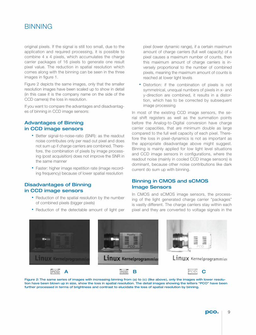
Figure 2 depicts the same images, only that the smaller resolution images have been scaled up to show in detail (in this case it is the company name on the side of the CCD camera) the loss in resolution.
If you want to compare the advantages and disadvantag-es of binning in CCD image sensors:
Advantages of Binningin CCD image sensors
Better signal-to-noise-ratio (SNR): as the readout noise contributes only per read out pixel and does not sum up if charge carriers are combined. There-fore, the combination of pixels by image process-ing (post acquisition) does not improve the SNR in the same manner
Faster: higher image repetition rate (image record-ing frequency) because of lower spatial resolution
Disadvantages of Binningin CCD image sensors
Reduction of the spatial resolution by the number of combined pixels (bigger pixels)
Reduction of the detectable amount of light per
pixel (lower dynamic range), if a certain maximum amount of charge carriers (full well capacity) of a pixel causes a maximum number of counts, then this maximum amount of charge carriers is in-versely proportional to the number of combined pixels, meaning the maximum amount of counts is reached at lower light levels
Distortion: if the combination of pixels is not symmetrical, unequal numbers of pixels in x- and y-direction are combined, it results in a distor-tion, which has to be corrected by subsequent image processing
In most of the existing CCD image sensors, the se-rial shift registers as well as the summation points before the Analog-to-Digital conversion have charge carrier capacities, that are minimum double as large compared to the full well capacity of each pixel. There-fore the loss in pixel-dynamics is not as important as the appropriate disadvantage above might suggest. Binning is mainly applied for low light level situations and CCD image sensors in confi gurations, where the readout noise (mainly in cooled CCD image sensors) is dominant, because other noise contributions like dark current do sum up with binning.
Binning in CMOS and sCMOSImage Sensors
In CMOS and sCMOS image sensors, the process-ing of the light generated charge carrier “packages” is vastly different. The charge carriers stay within each pixel and they are converted to voltage signals in the
Figure 2: The same series of images with increasing binning from (a) to (c) (like above), only the images with lower resolu-tion have been blown up in size, show the loss in spatial resolution. The detail images showing the letters “PCO” have been further processed in terms of brightness and contrast to elucidate the loss of spatial resolution by binning.
A B C
BINNING
9
WHY IS BINNINGDIFFERENT IN CMOSIMAGE SENSORS COMPAREDTO CCD IMAGE SENSORS?
The fundamental reason for the difference is the difference in technology and how the corresponding signals, the light induced charge carriers are treated and processed. Further, due to the historical pathway, at fi rst, “binning” was introduced in CCD image sensors. CCD image sen-sors allow for lossless transport of charge carrier pack-ages through their storage locations called registers, and they enable a lossless accumulation or summation of the charge carrier packages. Both of these features enabled “binning” to improve the signal-to-noise ratio.
Binning in CCD Image Sensors
The combination of the charge carrier content (generated by the impinging light signal) of two or more pixels of a CCD image sensor to form a new so-called super pix-el prior to readout and digitizing is called “binning.” This results in a summation of the generated charge carriers
from the single pixels, and it is usually done in the hor-izontal readout registers. The biggest advantage is the improvement of the signal-to-noise-ratio (SNR). Since the signal is increased before the readout process adds its noise contribution, allowing the recording of useful imag-es even at very low light levels, but on cost of a reduction in spatial resolution of the images.
Figure 1 illustrates the improvement in signal along with the reduction in resolution. Binning usually is ap-plied, if the signal, which should be recorded is weak and near to the noise level. The fi rst image on the left side is the result of a weak illumination with the full resolution of 640x480 pixels of the CCD image sensor. Some details can be spotted, but the image in general is very dim. The middle image in fi gure 1b shows the result of a 2 x 2 pixel binning, therefore per resulting pixel the signal is the summation of the content of 4
A
BC
Figure 1: Image (a) shows an image at a resolution of 640x480 pixels (VGA). Image (b), having the same exposure settings as the left, corresponds with 2 binned pixels in x- and y-direction to a resolution of 320x240 pixels. Image (c) with the highest brightness shows a 4x4 binning, therefore 16 pixels form the new super pixel resulting in a resolution of 160x120 pixels.
original pixels. If the signal is still too small, due to the application and required processing, it is possible to combine 4 x 4 pixels, which accumulates the charge carrier packages of 16 pixels to generate one result pixel value. The reduction in spatial resolution which comes along with the binning can be seen in the three images in fi gure 1.
Figure 2 depicts the same images, only that the smaller resolution images have been scaled up to show in detail (in this case it is the company name on the side of the CCD camera) the loss in resolution.
If you want to compare the advantages and disadvantag-es of binning in CCD image sensors:
Advantages of Binningin CCD image sensors
Better signal-to-noise-ratio (SNR): as the readout noise contributes only per read out pixel and does not sum up if charge carriers are combined. There-fore, the combination of pixels by image process-ing (post acquisition) does not improve the SNR in the same manner
Faster: higher image repetition rate (image record-ing frequency) because of lower spatial resolution
Disadvantages of Binningin CCD image sensors
Reduction of the spatial resolution by the number of combined pixels (bigger pixels)
Reduction of the detectable amount of light per
pixel (lower dynamic range), if a certain maximum amount of charge carriers (full well capacity) of a pixel causes a maximum number of counts, then this maximum amount of charge carriers is in-versely proportional to the number of combined pixels, meaning the maximum amount of counts is reached at lower light levels
Distortion: if the combination of pixels is not symmetrical, unequal numbers of pixels in x- and y-direction are combined, it results in a distor-tion, which has to be corrected by subsequent image processing
In most of the existing CCD image sensors, the se-rial shift registers as well as the summation points before the Analog-to-Digital conversion have charge carrier capacities, that are minimum double as large compared to the full well capacity of each pixel. There-fore the loss in pixel-dynamics is not as important as the appropriate disadvantage above might suggest. Binning is mainly applied for low light level situations and CCD image sensors in confi gurations, where the readout noise (mainly in cooled CCD image sensors) is dominant, because other noise contributions like dark current do sum up with binning.
Binning in CMOS and sCMOSImage Sensors
In CMOS and sCMOS image sensors, the process-ing of the light generated charge carrier “packages” is vastly different. The charge carriers stay within each pixel and they are converted to voltage signals in the
Figure 2: The same series of images with increasing binning from (a) to (c) (like above), only the images with lower resolu-tion have been blown up in size, show the loss in spatial resolution. The detail images showing the letters “PCO” have been further processed in terms of brightness and contrast to elucidate the loss of spatial resolution by binning.
A B C
BINNING

10
Disadvantages of Binning in CMOS and sCMOS image sensors
Reduction of the spatial resolution by the number of combined pixels
Additional time consumption either in the camera or in the computer, which could be relevant for large resolution image sensors
If the combination of pixels is not symmetrical, un-equal numbers of pixels in x- and y-direction are combined, it results in a distortion, which has to be corrected by subsequent image processing
At last, what’s the difference inbinning of CCD and CMOS(sCMOS) image sensors?
As mentioned previously, the binning process is tech-nically and fundamentally different in CCD and CMOS image sensors. In CCD image sensors there is a larger improvement of the signal-to-noise-ratio, since the signal is increased while the total readout noise stays constant. Only in emCCD image sensors it is a bit more complex, since more noise sources have to be added due to the additional amplifi cation noise caused by the impact ion-ization based multiplication process and the clock noise. In CMOS image sensors without charge mode binning capability the improvement of the signal-to-noise-ratio is
A
B
C
Figure 4: A 512 x 512 pixel image of neurons (a) and two “binned” images with a 2x2 average (b) of the starting image and a 4x4 average (c) to show the impact of pixel value averaging in weakly illuminated images regarding signal-to-noise and reso-lution. The scaling of all images is the same.
BINNING
smaller, since it is identical to the improvement by aver-aging of noisy signals.
Fortunately, recent sCMOS image sensors have been im-proved and become very sensitive, such that the combi-nation of more than 90 % quantum effi ciency and a very low readout noise enables low light measurements even without binning.
Figure 3: A 512 x 512 pixel image of neurons (a) and two “binned” images with a 2x2 summation (b) of the starting imageand a 4x4 summation (c) to show the impact of pixel value summation in weakly illuminated images regarding brightnessand resolution. The scaling of all images is the same.
pixels themselves. A few recent methods exist to sum charge carrier packages even in CMOS image sen-sors. This requires more electrical inter-connections between each pixel, which would make the timing con-trol more complex and it would signifi cantly decrease the fi ll factor (making a sensor less sensitive by de-creasing the quantum effi ciency). Thus, the underlying hardware “binning” that CCD image sensors display (the increase of the charge carrier package before the conversion into a voltage signal) is meanwhile realized in few recent sensor designs, but it was not available in most of the existing sCMOS and CMOS image sensors in the past due to the before mentioned complexity. Instead a mathematical "binning" has been used to im-prove the signal-to-noise-ratio. This could be either a summation of the pixel values (fi gure 3) to get a better brightness in the image or it can be an averaging of the corresponding pixel values (fi gure 4) to improve the signal-to-noise ratio.
Binning with Summation
In case of CMOS pixel summation, simply all the involved pixel values are added, which behaves very similar to the real “binning” in CCD image sensors, which can be seen in fi gure 3, where the highest binning (fi gure 3c), 4x4, re-sults in the brightest image. But the improvement in sig-nal-to-noise ratio is smaller compared to the CCD bin-ning, improving by a factor of the square root of 2. If this is done in a camera or later in a post processing in the
computer, care has to be taken not to get an overfl ow, since now 25 % signal in each pixel will generate a 100 % value in case of a 2x2 binning.
Binning with Averaging
The binning with averaging improves the signal-to-noise ratio only by the square root of 2, but it doesn’t result in brighter images, as can be seen by the examples in fi g-ure 4. From left to right a 512x512 pixel image is binned by 2x2 and 4x4 and the signal to noise ratio is improved (diffi cult to see) but the brightness remains constant while the resolution becomes smaller. If averaging as process is used, no attention has to be paid to overfl ow. If you want to compare the advantages and disadvan-tages of mathematical “binning” in CMOS and sCMOS image sensors:
Advantages of Binning in CMOSand sCMOS image sensors
Slight improvement of signal-to-noise-ratio (SNR), because the combination of 4 pixel val-ues will improve the signal-to-noise ratio by the square root of 2.
Higher image transfer rate because of lower amount of image data (could be relevant if the camera has a data interface with a low bandwidth like USB2.0)
BINNING
A
B
C

11
Disadvantages of Binning in CMOS and sCMOS image sensors
Reduction of the spatial resolution by the number of combined pixels
Additional time consumption either in the camera or in the computer, which could be relevant for large resolution image sensors
If the combination of pixels is not symmetrical, un-equal numbers of pixels in x- and y-direction are combined, it results in a distortion, which has to be corrected by subsequent image processing
At last, what’s the difference inbinning of CCD and CMOS(sCMOS) image sensors?
As mentioned previously, the binning process is tech-nically and fundamentally different in CCD and CMOS image sensors. In CCD image sensors there is a larger improvement of the signal-to-noise-ratio, since the signal is increased while the total readout noise stays constant. Only in emCCD image sensors it is a bit more complex, since more noise sources have to be added due to the additional amplifi cation noise caused by the impact ion-ization based multiplication process and the clock noise. In CMOS image sensors without charge mode binning capability the improvement of the signal-to-noise-ratio is
A
B
C
Figure 4: A 512 x 512 pixel image of neurons (a) and two “binned” images with a 2x2 average (b) of the starting image and a 4x4 average (c) to show the impact of pixel value averaging in weakly illuminated images regarding signal-to-noise and reso-lution. The scaling of all images is the same.
BINNING
smaller, since it is identical to the improvement by aver-aging of noisy signals.
Fortunately, recent sCMOS image sensors have been im-proved and become very sensitive, such that the combi-nation of more than 90 % quantum effi ciency and a very low readout noise enables low light measurements even without binning.
Figure 3: A 512 x 512 pixel image of neurons (a) and two “binned” images with a 2x2 summation (b) of the starting imageand a 4x4 summation (c) to show the impact of pixel value summation in weakly illuminated images regarding brightnessand resolution. The scaling of all images is the same.
pixels themselves. A few recent methods exist to sum charge carrier packages even in CMOS image sen-sors. This requires more electrical inter-connections between each pixel, which would make the timing con-trol more complex and it would signifi cantly decrease the fi ll factor (making a sensor less sensitive by de-creasing the quantum effi ciency). Thus, the underlying hardware “binning” that CCD image sensors display (the increase of the charge carrier package before the conversion into a voltage signal) is meanwhile realized in few recent sensor designs, but it was not available in most of the existing sCMOS and CMOS image sensors in the past due to the before mentioned complexity. Instead a mathematical "binning" has been used to im-prove the signal-to-noise-ratio. This could be either a summation of the pixel values (fi gure 3) to get a better brightness in the image or it can be an averaging of the corresponding pixel values (fi gure 4) to improve the signal-to-noise ratio.
Binning with Summation
In case of CMOS pixel summation, simply all the involved pixel values are added, which behaves very similar to the real “binning” in CCD image sensors, which can be seen in fi gure 3, where the highest binning (fi gure 3c), 4x4, re-sults in the brightest image. But the improvement in sig-nal-to-noise ratio is smaller compared to the CCD bin-ning, improving by a factor of the square root of 2. If this is done in a camera or later in a post processing in the
computer, care has to be taken not to get an overfl ow, since now 25 % signal in each pixel will generate a 100 % value in case of a 2x2 binning.
Binning with Averaging
The binning with averaging improves the signal-to-noise ratio only by the square root of 2, but it doesn’t result in brighter images, as can be seen by the examples in fi g-ure 4. From left to right a 512x512 pixel image is binned by 2x2 and 4x4 and the signal to noise ratio is improved (diffi cult to see) but the brightness remains constant while the resolution becomes smaller. If averaging as process is used, no attention has to be paid to overfl ow. If you want to compare the advantages and disadvan-tages of mathematical “binning” in CMOS and sCMOS image sensors:
Advantages of Binning in CMOSand sCMOS image sensors
Slight improvement of signal-to-noise-ratio (SNR), because the combination of 4 pixel val-ues will improve the signal-to-noise ratio by the square root of 2.
Higher image transfer rate because of lower amount of image data (could be relevant if the camera has a data interface with a low bandwidth like USB2.0)
BINNING
A
B
C

12
Pixel Size & Fill Factor
The fi ll factor (see fi gure 4) of a pixel describes the ratio of light sensitive area versus total area of a pixel, since a part of the area of an image sensor pixel is always used for transistors, wiring, capacitors or registers, which be-long to the structure of the pixel of the corresponding image sensor (CCD, CMOS, sCMOS). Only the light sen-sitive part might contribute to the light to charge carrier conversion, which is detected.
For camera systems, it is usually the QE of the whole camera system which is given. This includes non-mate-rial related losses like fi ll-factor and refl ection of windows and cover glasses. In data sheets, this parameter is given as a percentage, such that a QE of 50 % means that on average two photons are required to generate one charge carrier (electron).
Figure 3: Measured re� ectivity of silicon as material used in solar cells3.
Figure 4: Pixels with different � ll factors (blue area corre-sponds to light sensitive area): [a] pixel with 75 % � ll factor, [b] pixel with 50 % � ll factor and [c] pixel with 50 % � ll factor plus micro lens on top.
Figure 5: Cross sectional view of pixels with different � ll fac-tors (blue area corresponds to light sensitive area) and the light rays which impinge on them (orange arrows). Dashed light rays indicate that this light does not contribute to the signal: [a] pixel with 75 % � ll factor, [b] pixel with 50 % � ll fac-tor and [c] pixel with 50 % � ll factor plus micro lens on top.
PIXEL SIZE & SENSITIVITY
In case the fi ll factor is too small4, fi ll factor is usually im-proved with the addition of micro lenses. The lens col-lects the light impinging onto the pixel and focuses the light to the light sensitive area of the pixel (see fi gure 5).
Fill factorLight
sensitive areaQuantumeffi ciency
Signal
large large high large
small small small small
small +micro lens
larger effective area
high large
Table 1: Correspondences & Relations
Although the application of micro lenses is always benefi cial for pixel with fi ll factors below 100 %, there are some phys-ical and technological limitations to consider. (See Table 2)
Pixel Size & Optical Imaging
Figure 6 demonstrates optical imaging with a simple op-tical system based on a thin lens. In this situation, the Newtonian imaging equation is valid:
x0 ∙ xi = f
This is illustrated in fi gure 2, which shows the spectrally dependent absorption coeffi cient (see fi g. 2 – blue curve) of silicon as used in solar cells. The second curve (see fi g. 2 – red curve) depicts the penetration depth of light in sil-icon and is the inverse of the blue curve. In this scenario, it is very likely that the material used had no AR-coating. This paper, by Green and Keevers², also measured the spectrally dependent refl ectivity of silicon. This is shown in fi gure 3. The curve represents the factor, R, in the above equation for the quantum effi ciency.
ARE LARGER PIXELSALWAYS MORE SENSITIVE?
There is a common myth that larger pixel size image sen-sors are always more sensitive than smaller pixel size image sensors. This isn’t always the case, though. To explain why this is more a myth than a fact, it is a good idea to look at how the pixel size of an image sensor has an impact on the image quality, especially for the overall sensitivity, which is determined by the quantum effi ciency.
Quantum Ef� ciency
The "quantum effi ciency" (QE) of a photo detector or image sensor describes the ratio of incident photons to converted charge carriers which are read out as a signal from the de-vice. In a CCD, CMOS or sCMOS camera it denotes how ef-fi ciently the camera converts light into electric charges and it is therefore a very good parameter to compare the sensitivity of such a system. When light or photons fall onto a semicon-ductor - such as silicon - there are several loss mechanisms.
semiconductor and partially travels through it. As the or-ange curve of the photon fl ux shows, a part of it is lost at the surface via refl ection, therefore a proper anti-refl ective coating has a high impact on this loss contribution.
Following this a part of the photon fl ux is converted into charge carriers in the light sensitive part of the semicon-ductor, and a remaining part is transmitted. Using this illus-tration the quantum effi ciency can be defi ned as:
QE = (1 − R) ∙ ζ ∙ (1− e−α∙d)
with:
(1 − R) Refl ection at the surface, which can be min-imized by appropriate coatings
ζ Part of the electron-hole-pairs (charge carri-ers), which contribute to the photo current, and which did not recombine at the surface.
(1− e−α∙d) Part of the photon fl ux, which is absorbed in the semiconductor. Therefore the thickness d should be suffi ciently large, to increase that part.
Due to the different absorption characteristics of silicon, as basic material for these image sensors and due to the different structures of each image sensor the QE is spectrally dependent.
x x
d
1/αphoto
sensi�vevolume
photons incidentphoton
flux
reflectedphoton
flux
transmi�edphoton
flux
semiconductormaterial
Figure 1: Semiconductor material with the thickness, d, and a light sensitive area or volume which converts photons into charge carriers. The graph shows what happens with the photon � ux across the light penetration into the material1.
Figure 2: Measured absorption coef� cients and penetration depth from silicon as material used in solar cells2.
Figure 1 shows the photons impinging on a semiconductor with a light sensitive area. The fi gure also shows a curve, which represents the photon fl ux when the light hits the

13
Pixel Size & Fill Factor
The fi ll factor (see fi gure 4) of a pixel describes the ratio of light sensitive area versus total area of a pixel, since a part of the area of an image sensor pixel is always used for transistors, wiring, capacitors or registers, which be-long to the structure of the pixel of the corresponding image sensor (CCD, CMOS, sCMOS). Only the light sen-sitive part might contribute to the light to charge carrier conversion, which is detected.
For camera systems, it is usually the QE of the whole camera system which is given. This includes non-mate-rial related losses like fi ll-factor and refl ection of windows and cover glasses. In data sheets, this parameter is given as a percentage, such that a QE of 50 % means that on average two photons are required to generate one charge carrier (electron).
Figure 3: Measured re� ectivity of silicon as material used in solar cells3.
Figure 4: Pixels with different � ll factors (blue area corre-sponds to light sensitive area): [a] pixel with 75 % � ll factor, [b] pixel with 50 % � ll factor and [c] pixel with 50 % � ll factor plus micro lens on top.
Figure 5: Cross sectional view of pixels with different � ll fac-tors (blue area corresponds to light sensitive area) and the light rays which impinge on them (orange arrows). Dashed light rays indicate that this light does not contribute to the signal: [a] pixel with 75 % � ll factor, [b] pixel with 50 % � ll fac-tor and [c] pixel with 50 % � ll factor plus micro lens on top.
PIXEL SIZE & SENSITIVITY
In case the fi ll factor is too small4, fi ll factor is usually im-proved with the addition of micro lenses. The lens col-lects the light impinging onto the pixel and focuses the light to the light sensitive area of the pixel (see fi gure 5).
Fill factorLight
sensitive areaQuantumeffi ciency
Signal
large large high large
small small small small
small +micro lens
larger effective area
high large
Table 1: Correspondences & Relations
Although the application of micro lenses is always benefi cial for pixel with fi ll factors below 100 %, there are some phys-ical and technological limitations to consider. (See Table 2)
Pixel Size & Optical Imaging
Figure 6 demonstrates optical imaging with a simple op-tical system based on a thin lens. In this situation, the Newtonian imaging equation is valid:
x0 ∙ xi = f
This is illustrated in fi gure 2, which shows the spectrally dependent absorption coeffi cient (see fi g. 2 – blue curve) of silicon as used in solar cells. The second curve (see fi g. 2 – red curve) depicts the penetration depth of light in sil-icon and is the inverse of the blue curve. In this scenario, it is very likely that the material used had no AR-coating. This paper, by Green and Keevers², also measured the spectrally dependent refl ectivity of silicon. This is shown in fi gure 3. The curve represents the factor, R, in the above equation for the quantum effi ciency.
ARE LARGER PIXELSALWAYS MORE SENSITIVE?
There is a common myth that larger pixel size image sen-sors are always more sensitive than smaller pixel size image sensors. This isn’t always the case, though. To explain why this is more a myth than a fact, it is a good idea to look at how the pixel size of an image sensor has an impact on the image quality, especially for the overall sensitivity, which is determined by the quantum effi ciency.
Quantum Ef� ciency
The "quantum effi ciency" (QE) of a photo detector or image sensor describes the ratio of incident photons to converted charge carriers which are read out as a signal from the de-vice. In a CCD, CMOS or sCMOS camera it denotes how ef-fi ciently the camera converts light into electric charges and it is therefore a very good parameter to compare the sensitivity of such a system. When light or photons fall onto a semicon-ductor - such as silicon - there are several loss mechanisms.
semiconductor and partially travels through it. As the or-ange curve of the photon fl ux shows, a part of it is lost at the surface via refl ection, therefore a proper anti-refl ective coating has a high impact on this loss contribution.
Following this a part of the photon fl ux is converted into charge carriers in the light sensitive part of the semicon-ductor, and a remaining part is transmitted. Using this illus-tration the quantum effi ciency can be defi ned as:
QE = (1 − R) ∙ ζ ∙ (1− e−α∙d)
with:
(1 − R) Refl ection at the surface, which can be min-imized by appropriate coatings
ζ Part of the electron-hole-pairs (charge carri-ers), which contribute to the photo current, and which did not recombine at the surface.
(1− e−α∙d) Part of the photon fl ux, which is absorbed in the semiconductor. Therefore the thickness d should be suffi ciently large, to increase that part.
Due to the different absorption characteristics of silicon, as basic material for these image sensors and due to the different structures of each image sensor the QE is spectrally dependent.
x x
d
1/αphoto
sensi�vevolume
photons incidentphoton
flux
reflectedphoton
flux
transmi�edphoton
flux
semiconductormaterial
Figure 1: Semiconductor material with the thickness, d, and a light sensitive area or volume which converts photons into charge carriers. The graph shows what happens with the photon � ux across the light penetration into the material1.
Figure 2: Measured absorption coef� cients and penetration depth from silicon as material used in solar cells2.
Figure 1 shows the photons impinging on a semiconductor with a light sensitive area. The fi gure also shows a curve, which represents the photon fl ux when the light hits the

14
Of even more importance for practical usage than the depth of focus is the depth of � eld. The depth of � eld is the range of object positions for which the radius of the blur disk remains below a threshold ε at a � xed image plane.
𝑑 ± Δ𝑥3 = −𝑓2
𝑑’ ∓ 𝑓/# ⋅ (1 + |𝑀|) ⋅ 𝜀
In the limit of |Δ𝑥3| ≪ 𝑑 we obtain:
|Δ𝑥3| ≈ 𝑓/# ⋅ 1 + |𝑀|
𝑀2 ⋅ 𝜀
If the depth of � eld includes in� nite distance, the depth of � eld is given by:
𝑑𝑚𝑖𝑛 ≈ 𝑓0
2
2 ⋅ 𝑓/# ⋅ 𝜀Generally the whole concept of depth of � eld and depth of focus is only valid for a perfect optical system. If the optical system shows any aberrations, the depth of � eld can only be used for blurring signi� cantly larger than those caused by aberrations of the system.
Pixel Size & Comparison TotalArea / ResolutionIf the in� uence of the pixel size on the sensitivity, dynamic, image quality of a camera should be investigated, there
Figure 8: Illustration of the concept of depth of � eld. This gives the range of distances of the object in which the blur-ring of its image at a � xed image distance remains below a given threshold.
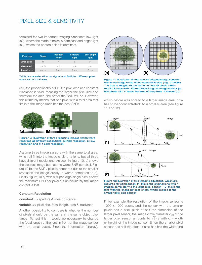
Figure 9: Illustration of two square shaped image sensors within the image circle of the same lens, which generates the image of a tree on the image sensors. Image sensor [a] has pixels a quarter the size area of the pixels of sensor [b].
For ease of comparison, we shall assume square shaped image sensors. These are � t into the image cir-cle or imaging area of a lens. For comparison, a homo-geneous illumination is assumed. Therefore, the radiant � ux per unit area, also called irradiance E [W/m2], is constant over the area of the image circle. Let us as-sume that the left image sensor (� g. 9, sensor [a]) has smaller pixels but higher resolution — e.g. 2000 x 2000 pixels at 10µm pixel pitch — while the right image sen-sor (� g. 9, sensor [b]) subsequently has 1000 x 1000 pixels at 20µm pixel pitch.
The question would be, which sensor has the brighter signal and which sensor has the better signal-to-noise-ratio (SNR)? To answer this question, it is possible to either look at a single pixel, which neglects the different resolution, or to compare the same resolution with the same lens, but this corresponds to comparing a single pixel with 4 pixels.
Generally, it is also assumed that both image sensors have the same � ll factor of their pixels. The small pixel measures the signal, m, which has its own readout noise, r0, and therefore a signal-to-noise-ratio, s, could be de-
PIXEL SIZE & SENSITIVITY
is known as depth of focus. The above equation can be solved for Δx3 and yields:
Δ𝑥3 = 𝑓/# ⋅ 1 +
𝑑’
𝑓0 ⋅ 𝜀 = 𝑓/# ⋅ (1 + |𝑀|) ⋅ 𝜀
where M is the magni� cation from chapter 2. This equation shows the critical role of the f-number for the depth of focus.
are various parameters that could be changed or kept constant. In this section, we’ll follow different pathways to try to answer this question.
Constant Area
constant => image circle, aperture, focal length, object distance & irradiance,
variable => resolution & pixel size
The image equation (chapter 2) determines the rela-tion between object and image distances. If the im-age plane is slightly shifted or the object is closer to the lens system, the image is not rendered useless. Rather, it gets more and more blurred the larger the deviation from the distances becomes, given by the image equation.
The concepts of depth of focus and depth of � eld are based on the fact that for any given application only a certain degree of sharpness is required. For digital image processing, it is naturally given by the size of the pixels of an image sensor. It makes no sense to resolve smaller structures but to allow a certain blurring. The blurring can be described using the image of a point object, as illustrated in � gure 6. At the image plane, the point object is imaged to a point. It smears to a disk with the radius, e, (see � gure 7) with increasing distance from the image plane.
Introducing the f-number f/# of an optical system as the ra-tio of the focal length f0 and diameter of lens aperture D0:
f/# = f0
D0
the radius of the blur disk can be expressed:
𝜀 = 1
f/#
⋅ 𝑓0
(𝑓0 + 𝑑’) ⋅ Δ𝑥3
where Δx3 is the distance from the (focused) image plane. The range of positions of the image plane, [d’ - Δx3, d’ +Δx3], for which the radius of the blur disk is lower than 𝜀,
Limitations
Size Limitation for micro lenses
Although micro lenses up to 20 µm pixel pitch can be manufac-tured, their ef� ciency gradually is decreased above 6-8 µm pixel pitch. The increased stack height, which is proprotional to the covered area, is not favorable as well.5
Front illuminated CMOS pixels have limited � ll factor
Due to semi-conductor processing requirements for front illuminated CMOS image sensors, there must always be a certain pixel area cov-ered with metal, which reduces the maximum available � ll factor.
Large light sensitive areas
Large areas are dif� cult to realize because the diffusion length, and therefore the probability for recom-bination, increases. Although image sensors for special applications have been realized with 100 µm pixel pitch.
Table 2: Some Limitations
Figure 6: Optical imaging with a simple optical system based on a thin lens and characterized by some geometrical pa-rameters: f - focal length of lens, Fo - focal point of lens on object side, Fi - focal point of lens on image side, xo - dis-tance between Fo and object = object distance, xi - distance between Fi and image, Yo - object size, Yi - image size
Figure 7: Illustration of the concept of depth of focus, which is the range of image distances in which the blurring of the image remains below a certain threshold.
PIXEL SIZE & SENSITIVITY
Or the Gaussian lens equation:
1
f =
1
(x0 + f ) +
1
(xi + f )
and the magni� cation, M, is given by the ratio of the im-age size Yi to the object size Y0:
M = Yi
Y0
= f
x0
= Xi
f
Pixel Size & Depth ofFocus / Depth of Field6

15
Of even more importance for practical usage than the depth of focus is the depth of � eld. The depth of � eld is the range of object positions for which the radius of the blur disk remains below a threshold ε at a � xed image plane.
𝑑 ± Δ𝑥3 = −𝑓2
𝑑’ ∓ 𝑓/# ⋅ (1 + |𝑀|) ⋅ 𝜀
In the limit of |Δ𝑥3| ≪ 𝑑 we obtain:
|Δ𝑥3| ≈ 𝑓/# ⋅ 1 + |𝑀|
𝑀2 ⋅ 𝜀
If the depth of � eld includes in� nite distance, the depth of � eld is given by:
𝑑𝑚𝑖𝑛 ≈ 𝑓0
2
2 ⋅ 𝑓/# ⋅ 𝜀Generally the whole concept of depth of � eld and depth of focus is only valid for a perfect optical system. If the optical system shows any aberrations, the depth of � eld can only be used for blurring signi� cantly larger than those caused by aberrations of the system.
Pixel Size & Comparison TotalArea / ResolutionIf the in� uence of the pixel size on the sensitivity, dynamic, image quality of a camera should be investigated, there
Figure 8: Illustration of the concept of depth of � eld. This gives the range of distances of the object in which the blur-ring of its image at a � xed image distance remains below a given threshold.
Figure 9: Illustration of two square shaped image sensors within the image circle of the same lens, which generates the image of a tree on the image sensors. Image sensor [a] has pixels a quarter the size area of the pixels of sensor [b].
For ease of comparison, we shall assume square shaped image sensors. These are � t into the image cir-cle or imaging area of a lens. For comparison, a homo-geneous illumination is assumed. Therefore, the radiant � ux per unit area, also called irradiance E [W/m2], is constant over the area of the image circle. Let us as-sume that the left image sensor (� g. 9, sensor [a]) has smaller pixels but higher resolution — e.g. 2000 x 2000 pixels at 10µm pixel pitch — while the right image sen-sor (� g. 9, sensor [b]) subsequently has 1000 x 1000 pixels at 20µm pixel pitch.
The question would be, which sensor has the brighter signal and which sensor has the better signal-to-noise-ratio (SNR)? To answer this question, it is possible to either look at a single pixel, which neglects the different resolution, or to compare the same resolution with the same lens, but this corresponds to comparing a single pixel with 4 pixels.
Generally, it is also assumed that both image sensors have the same � ll factor of their pixels. The small pixel measures the signal, m, which has its own readout noise, r0, and therefore a signal-to-noise-ratio, s, could be de-
PIXEL SIZE & SENSITIVITY
is known as depth of focus. The above equation can be solved for Δx3 and yields:
Δ𝑥3 = 𝑓/# ⋅ 1 +
𝑑’
𝑓0 ⋅ 𝜀 = 𝑓/# ⋅ (1 + |𝑀|) ⋅ 𝜀
where M is the magni� cation from chapter 2. This equation shows the critical role of the f-number for the depth of focus.
are various parameters that could be changed or kept constant. In this section, we’ll follow different pathways to try to answer this question.
Constant Area
constant => image circle, aperture, focal length, object distance & irradiance,
variable => resolution & pixel size
The image equation (chapter 2) determines the rela-tion between object and image distances. If the im-age plane is slightly shifted or the object is closer to the lens system, the image is not rendered useless. Rather, it gets more and more blurred the larger the deviation from the distances becomes, given by the image equation.
The concepts of depth of focus and depth of � eld are based on the fact that for any given application only a certain degree of sharpness is required. For digital image processing, it is naturally given by the size of the pixels of an image sensor. It makes no sense to resolve smaller structures but to allow a certain blurring. The blurring can be described using the image of a point object, as illustrated in � gure 6. At the image plane, the point object is imaged to a point. It smears to a disk with the radius, e, (see � gure 7) with increasing distance from the image plane.
Introducing the f-number f/# of an optical system as the ra-tio of the focal length f0 and diameter of lens aperture D0:
f/# = f0
D0
the radius of the blur disk can be expressed:
𝜀 = 1
f/#
⋅ 𝑓0
(𝑓0 + 𝑑’) ⋅ Δ𝑥3
where Δx3 is the distance from the (focused) image plane. The range of positions of the image plane, [d’ - Δx3, d’ +Δx3], for which the radius of the blur disk is lower than 𝜀,
Limitations
Size Limitation for micro lenses
Although micro lenses up to 20 µm pixel pitch can be manufac-tured, their ef� ciency gradually is decreased above 6-8 µm pixel pitch. The increased stack height, which is proprotional to the covered area, is not favorable as well.5
Front illuminated CMOS pixels have limited � ll factor
Due to semi-conductor processing requirements for front illuminated CMOS image sensors, there must always be a certain pixel area cov-ered with metal, which reduces the maximum available � ll factor.
Large light sensitive areas
Large areas are dif� cult to realize because the diffusion length, and therefore the probability for recom-bination, increases. Although image sensors for special applications have been realized with 100 µm pixel pitch.
Table 2: Some Limitations
Figure 6: Optical imaging with a simple optical system based on a thin lens and characterized by some geometrical pa-rameters: f - focal length of lens, Fo - focal point of lens on object side, Fi - focal point of lens on image side, xo - dis-tance between Fo and object = object distance, xi - distance between Fi and image, Yo - object size, Yi - image size
Figure 7: Illustration of the concept of depth of focus, which is the range of image distances in which the blurring of the image remains below a certain threshold.
PIXEL SIZE & SENSITIVITY
Or the Gaussian lens equation:
1
f =
1
(x0 + f ) +
1
(xi + f )
and the magni� cation, M, is given by the ratio of the im-age size Yi to the object size Y0:
M = Yi
Y0
= f
x0
= Xi
f
Pixel Size & Depth ofFocus / Depth of Field6
16
height and half the diagonal of the “old” image circle, which gives:
𝑑𝑛ℯ𝑤 = 22
⋅ 𝑐 = 1
2 ⋅ 𝑐
To get an idea of the required focal length, it is possible to determine the new magni� cation Mnew and subsequently the required focal length fnew of the lens (see chapter 2 and � gure 9), since the object size, Y0, remains the same:
𝑀𝑛ℯ𝑤 = |𝑌𝑛ℯ𝑤|
𝑌0
= |𝑌𝑜𝑙𝑑|
2
𝑌0
= 1
2 ⋅ 𝑀𝑜𝑙𝑑 𝑤𝑖𝑡h
𝑌𝑜𝑙𝑑
𝑌𝑛ℯ𝑤 = 12 ⋅ 𝑐
2 ⋅ 𝑐
Since the photon � ux, Φ0, coming from the object or a light source is constant due to the same aperture of the lens (NOT the same f-number!), the new lens with the changed focal length achieves to spread the same en-ergy over a smaller area, which results in a higher irradi-ance. To get an idea of the new irradiance, we need to know the new area, Anew:
𝐴𝑛ℯ𝑤
𝐴𝑜𝑙𝑑
= 𝜋 ⋅
12 ⋅ 𝑐2
2
𝜋 ⋅
2 ⋅ 𝑐2
2 =
1
4
With this new area it is possible to calculate how much higher the new irradiance, Inew, will be.
𝐼𝑛ℯ𝑤 = Φ0
𝐴𝑛ℯ𝑤
= Φ0
14 ⋅ 𝐴𝑜𝑙𝑑
= 4 ⋅ Φ0
𝐴𝑜𝑙𝑑
= 4 ⋅ 𝐼𝑜𝑙𝑑
The reason for that discrepancy between the argumentation and the results is within the de� nition of the f-number f/#:
f/# = f
D
Figure 13: Images of the same test chart with the same resolution, same object distance, and same � ll factor but dif-ferent pixel size and different lens settings (all images have the same scaling for display):[a] pixel size 14.8 µm x 14.8 µm, f = 100mm, f-number = 16[b] pixel size 7.4 µm x 7.4 µm, f = 50mm, f-number = 16[c] pixel size 7.4 µm x 7.4 µm, f = 50mm, f-number = 8
Pixel type SignalReadout
noiseSNR low
lightSNR bright
light
Small pixel m r0 s0 s1
Large pixel m > r0 < s0 s1
Table 4: consideration on signal and SNR for different pixel sizes same resolution
If now the argument would be that the larger f-number will cause a different depth of � eld, which will in turn change the sharpness of the image and therefore the quality, the equation from chapter 3 can be used to look at the consequences.
From the above example we have the focal lengths fold = 100mm and fnew = 50mm, and we are looking for the right f-number to have the same depth of � eld. Therefore:
𝑓2𝑜𝑙𝑑
2 ⋅ 𝑓/#𝑜𝑙𝑑 ⋅ 𝜀 =
𝑓2𝑛ℯ𝑤𝑜𝑙𝑑
2 ⋅ 𝑓/#𝑛ℯ𝑤 ⋅ 𝜀 <=> 𝑓/#𝑛ℯ𝑤 𝑓
2𝑛ℯ𝑤
𝑓2𝑜𝑙𝑑
⋅ 𝑓/#𝑜𝑙𝑑 = 502
1002 ⋅ 16 = 4
From the above example we have the focal lengths fold = 100mm and fnew = 50mm, and we are looking for the right f-number to have the same depth of � eld. Therefore:
Since we have calculated a f-number = 8 for the correct comparison, the depth of � eld for the image sensor with the smaller pixels is even better.
PIXEL SIZE & SENSITIVITY
The lenses are constructed such that the same f-number always generates the same irradiance in the same image circle area. Therefore, the attempt to focus the energy on a smaller area for the comparison is not accomplished by keeping the f-number constant. It is the real diameter of the aperture, D, which has to be kept constant. There-fore, the new f-number would be, if the old f-number was f/#=16 (see example in � gure 13):
𝑓/#𝑛ℯ𝑤 = 𝑓𝑛ℯ𝑤
𝐷0
= 𝑓𝑛ℯ𝑤
𝑓𝑜𝑙𝑑/𝑓/#𝑜𝑙𝑑
= 𝑓𝑛ℯ𝑤
𝑓𝑜𝑙𝑑
⋅ 𝑓/#𝑜𝑙𝑑 = 50
100 ⋅ 16 = 8
Again the question would be which sensor has the brighter signal and which sensor has the better signal-to-noise-ratio (SNR)? This time we look at the same number of pixels but with different size, but due to the different lens at the same aperture, the irradiance for the smaller pixels is higher. Still, it is assumed that both image sen-sors have the same � ll factor of their pixels.
Figure 10: Illustration of three resulting images which were recorded at different resolutions: a) high resolution, b) low resolution and c) 1 pixel resolution
Still, the proportionality of SNR to pixel area at a constant irradiance is valid, meaning the larger the pixel size and therefore the area, the better the SNR will be. However, this ultimately means that one pixel with a total area that � ts into the image circle has the best SNR:
Figure 11: Illustration of two square shaped image sensors within the image circle of the same lens type (e.g. f-mount). The tree is imaged to the same number of pixels which require lenses with different focal lengths: Image sensor [a] has pixels with 4 times the area of the pixels of sensor [b].
Figure 12: llustration of two imaging situations, which are required for comparison: [1] this is the original lens which images completely to the large pixel sensor - [2] this is the lens with the changed focal length, which images to the smaller pixel size sensor
termined for two important imaging situations: low light (s0), where the readout noise is dominant and bright light (s1), where the photon noise is dominant.
which before was spread to a larger image area, now has to be “concentrated” to a smaller area (see � gure 11 and 12).
PIXEL SIZE & SENSITIVITY
Pixel type SignalReadout
noiseSNR low
lightSNR bright
light
Small pixel m r0 s0 s1
Large pixel 4 x m > r0 > s0 > s1
4 small pixel 4 x m 2 x r07 2 x s0 2 x s1
Table 3: consideration on signal and SNR for different pixel sizes same total area
Assume three image sensors with the same total area, which all � t into the image circle of a lens, but all three have different resolutions. As seen in � gure 10, a) shows the clearest image but has the worst SNR per pixel. Fig-ure 10 b), the SNR / pixel is better but due to the smaller resolution the image quality is worse compared to a). Finally, � gure 10 c) with a super large single pixel shows the maximum SNR per pixel but unfortunately the image content is lost.
Constant Resolution
constant => aperture & object distance,
variable => pixel size, focal length, area & irradiance
Another possibility to compare is whether the number of pixels should be the same at the same object dis-tance. To test this, it would be necessary to change the focal length of the lens in front of the image sensor with the small pixels. Since the information (energy),
If, for example the resolution of the image sensor is 1000 x 1000 pixels, and the sensor with the smaller pixels has a pixel pitch of half the dimension of the larger pixel sensor, the image circle diameter dold of the larger pixel sensor amounts to 2 ∙ 𝑐 with c = width or height of the image sensor. Since the smaller pixel sensor has half the pitch, it also has half the width and

17
height and half the diagonal of the “old” image circle, which gives:
𝑑𝑛ℯ𝑤 = 22
⋅ 𝑐 = 1
2 ⋅ 𝑐
To get an idea of the required focal length, it is possible to determine the new magni� cation Mnew and subsequently the required focal length fnew of the lens (see chapter 2 and � gure 9), since the object size, Y0, remains the same:
𝑀𝑛ℯ𝑤 = |𝑌𝑛ℯ𝑤|
𝑌0
= |𝑌𝑜𝑙𝑑|
2
𝑌0
= 1
2 ⋅ 𝑀𝑜𝑙𝑑 𝑤𝑖𝑡h
𝑌𝑜𝑙𝑑
𝑌𝑛ℯ𝑤 = 12 ⋅ 𝑐
2 ⋅ 𝑐
Since the photon � ux, Φ0, coming from the object or a light source is constant due to the same aperture of the lens (NOT the same f-number!), the new lens with the changed focal length achieves to spread the same en-ergy over a smaller area, which results in a higher irradi-ance. To get an idea of the new irradiance, we need to know the new area, Anew:
𝐴𝑛ℯ𝑤
𝐴𝑜𝑙𝑑
= 𝜋 ⋅
12 ⋅ 𝑐2
2
𝜋 ⋅
2 ⋅ 𝑐2
2 =
1
4
With this new area it is possible to calculate how much higher the new irradiance, Inew, will be.
𝐼𝑛ℯ𝑤 = Φ0
𝐴𝑛ℯ𝑤
= Φ0
14 ⋅ 𝐴𝑜𝑙𝑑
= 4 ⋅ Φ0
𝐴𝑜𝑙𝑑
= 4 ⋅ 𝐼𝑜𝑙𝑑
The reason for that discrepancy between the argumentation and the results is within the de� nition of the f-number f/#:
f/# = f
D
Figure 13: Images of the same test chart with the same resolution, same object distance, and same � ll factor but dif-ferent pixel size and different lens settings (all images have the same scaling for display):[a] pixel size 14.8 µm x 14.8 µm, f = 100mm, f-number = 16[b] pixel size 7.4 µm x 7.4 µm, f = 50mm, f-number = 16[c] pixel size 7.4 µm x 7.4 µm, f = 50mm, f-number = 8
Pixel type SignalReadout
noiseSNR low
lightSNR bright
light
Small pixel m r0 s0 s1
Large pixel m > r0 < s0 s1
Table 4: consideration on signal and SNR for different pixel sizes same resolution
If now the argument would be that the larger f-number will cause a different depth of � eld, which will in turn change the sharpness of the image and therefore the quality, the equation from chapter 3 can be used to look at the consequences.
From the above example we have the focal lengths fold = 100mm and fnew = 50mm, and we are looking for the right f-number to have the same depth of � eld. Therefore:
𝑓2𝑜𝑙𝑑
2 ⋅ 𝑓/#𝑜𝑙𝑑 ⋅ 𝜀 =
𝑓2𝑛ℯ𝑤𝑜𝑙𝑑
2 ⋅ 𝑓/#𝑛ℯ𝑤 ⋅ 𝜀 <=> 𝑓/#𝑛ℯ𝑤 𝑓
2𝑛ℯ𝑤
𝑓2𝑜𝑙𝑑
⋅ 𝑓/#𝑜𝑙𝑑 = 502
1002 ⋅ 16 = 4
From the above example we have the focal lengths fold = 100mm and fnew = 50mm, and we are looking for the right f-number to have the same depth of � eld. Therefore:
Since we have calculated a f-number = 8 for the correct comparison, the depth of � eld for the image sensor with the smaller pixels is even better.
PIXEL SIZE & SENSITIVITY
The lenses are constructed such that the same f-number always generates the same irradiance in the same image circle area. Therefore, the attempt to focus the energy on a smaller area for the comparison is not accomplished by keeping the f-number constant. It is the real diameter of the aperture, D, which has to be kept constant. There-fore, the new f-number would be, if the old f-number was f/#=16 (see example in � gure 13):
𝑓/#𝑛ℯ𝑤 = 𝑓𝑛ℯ𝑤
𝐷0
= 𝑓𝑛ℯ𝑤
𝑓𝑜𝑙𝑑/𝑓/#𝑜𝑙𝑑
= 𝑓𝑛ℯ𝑤
𝑓𝑜𝑙𝑑
⋅ 𝑓/#𝑜𝑙𝑑 = 50
100 ⋅ 16 = 8
Again the question would be which sensor has the brighter signal and which sensor has the better signal-to-noise-ratio (SNR)? This time we look at the same number of pixels but with different size, but due to the different lens at the same aperture, the irradiance for the smaller pixels is higher. Still, it is assumed that both image sen-sors have the same � ll factor of their pixels.
Figure 10: Illustration of three resulting images which were recorded at different resolutions: a) high resolution, b) low resolution and c) 1 pixel resolution
Still, the proportionality of SNR to pixel area at a constant irradiance is valid, meaning the larger the pixel size and therefore the area, the better the SNR will be. However, this ultimately means that one pixel with a total area that � ts into the image circle has the best SNR:
Figure 11: Illustration of two square shaped image sensors within the image circle of the same lens type (e.g. f-mount). The tree is imaged to the same number of pixels which require lenses with different focal lengths: Image sensor [a] has pixels with 4 times the area of the pixels of sensor [b].
Figure 12: llustration of two imaging situations, which are required for comparison: [1] this is the original lens which images completely to the large pixel sensor - [2] this is the lens with the changed focal length, which images to the smaller pixel size sensor
termined for two important imaging situations: low light (s0), where the readout noise is dominant and bright light (s1), where the photon noise is dominant.
which before was spread to a larger image area, now has to be “concentrated” to a smaller area (see � gure 11 and 12).
PIXEL SIZE & SENSITIVITY
Pixel type SignalReadout
noiseSNR low
lightSNR bright
light
Small pixel m r0 s0 s1
Large pixel 4 x m > r0 > s0 > s1
4 small pixel 4 x m 2 x r07 2 x s0 2 x s1
Table 3: consideration on signal and SNR for different pixel sizes same total area
Assume three image sensors with the same total area, which all � t into the image circle of a lens, but all three have different resolutions. As seen in � gure 10, a) shows the clearest image but has the worst SNR per pixel. Fig-ure 10 b), the SNR / pixel is better but due to the smaller resolution the image quality is worse compared to a). Finally, � gure 10 c) with a super large single pixel shows the maximum SNR per pixel but unfortunately the image content is lost.
Constant Resolution
constant => aperture & object distance,
variable => pixel size, focal length, area & irradiance
Another possibility to compare is whether the number of pixels should be the same at the same object dis-tance. To test this, it would be necessary to change the focal length of the lens in front of the image sensor with the small pixels. Since the information (energy),
If, for example the resolution of the image sensor is 1000 x 1000 pixels, and the sensor with the smaller pixels has a pixel pitch of half the dimension of the larger pixel sensor, the image circle diameter dold of the larger pixel sensor amounts to 2 ∙ 𝑐 with c = width or height of the image sensor. Since the smaller pixel sensor has half the pitch, it also has half the width and

18
WHAT IS ALL THE HYPEABOUT RESOLUTION ANDMEGA PIXELS ANYWAY?
Resolution, in the context of an image sensor, describes the total number of pixels utilized to create an image. Characterizing the resolution of an image sensor simply refers to the pixel count and is generally expressed as the horizontal number of pixels multiplied by the vertical number of pixels, for example:
𝑛𝑢𝑚𝑏ℯ𝑟 𝑜𝑓 𝑝𝑖𝑥ℯ𝑙h𝑜𝑟𝑖𝑧𝑜𝑛𝑡𝑎𝑙 × 𝑛𝑢𝑚𝑏ℯ𝑟 𝑜𝑓 𝑝𝑖𝑥ℯ𝑙𝑣ℯ𝑟𝑡𝑖𝑐𝑎𝑙
= 𝑡𝑜𝑡𝑎𝑙 𝑛𝑢𝑚𝑏ℯ𝑟 𝑜𝑓 𝑝𝑖𝑥ℯ𝑙
For instance, the sCMOS image sensor CIS2521 has the following resolution:
(2560h𝑜𝑟𝑖𝑧𝑜𝑛𝑡𝑎𝑙 × 2160𝑣ℯ𝑟𝑡𝑖𝑐𝑎𝑙) 𝑝𝑖𝑥ℯ𝑙 = 5.5 𝑀𝑝𝑖𝑥ℯ𝑙
The above calculation is typical for technical data sheets and marketing materials for scientifi c cameras, and would seem that more pixels would always be benefi cial, but the title question remains, why does the pixel count matter?
Bene� t and Relevancefor a Camera User
Assuming an image sensor, or a camera system with an im-age sensor, is generally used to detect images and objects, the critical question is what the infl uence of the resolution is on the image quality. First, if the resolution is higher, more spatial information is obtained, and as a consequence, larger data fi les are generated. Second, the amount of in-formation, which can be obtained by a camera, is insep-arably connected to the applied imaging optics, and the optics are characterized by their own optical resolution or ability to resolve details and must also be considered.
Figure 1 illustrates the infl uence of resolution between its limits of “Blurred” and “Sharp”, and the infl uence of contrast between its limits of “soft” and “brilliant” on the image quality, where, the higher the resolution of an op-tical system (consisting of a camera and imaging optics),
the more the images become “sharp”, while a “brilliant” contrast helps to distinguish the white and black lines even if they are not sharp.
Image Sensors and Cameras
Starting with the image sensor in a camera system, the modulation transfer function (MTF) describes the ability of the camera system to resolve fi ne structures. It is a variant of the optical transfer function1 (OTF) which mathematically describes how the system handles the optical information, or contrast of the scene or the sample, and transfers it onto the image sensor and then into a digital format for process-ing via computer. The resolution ability depends on both the number and also the size of the pixel.
The maximum spatial resolution is described as the abil-ity to separate patterns of black and white lines and it is given in line pairs per millimeter ([lp/mm]). The theoretical limit is given in the literature and defi nes the maximum
Figure 1: The graph illustrates how a black/white line test image is in� uenced between the limits “blurred” – “sharp” in resolution (y-axis) and between the limits “soft” – “brilliant” in contrast (x-axis).
PIXEL SIZE & SENSITIVITY
How to Compare Cameras WithRespect To Pixel Size & Sensitivity
Generally it is a good idea to image the same scene to each camera, which means:
Keep the object distance and the illuminationconstant!
If the cameras should be compared, they should use the same resolution, which either means analogue binning or mathematical summation or averaging, or usage of a region/area of interest.
Keep or adjust the same resolution for all cameras!
Then select a proper focal length for each camera, whereas each camera should see the same image on the active image sensor area.
Select corresponding lens with the appropriate fo-cal length for each camera!
Adjust the lens with the largest focal length with the largest useful f-number!
For a proper comparison use the equation for the f-number on page 17, keep the aperture D constant, and calculate the corresponding f-number for the other lenses and adjust them as good as possible - then compare the images!
Pixel typeLight
sensitive area
Fullwell capacity
Dark current Capacity Readout
noise
Small pixel small small small small small
Large pixel large large large large large
Table 5: consideration on fullwell capacity, readout noise, dark current
END NOTES
1 Graphic has been inspired by fi gure 17.1-1 from “Fundamentals of Photonics”, B.E.A. Saleh and M.C. Teich, John Wiley & Sons, Inc., 1991.
2 Data are taken from Green, M.A. and Keevers, M. “Optical properties of intrinsic silicon at 300 K”, Progress in Photovoltaics, p.189-92, vol.3, no.3; (1995).
3 Data are taken from Green, M.A. and Keevers, M. “Optical properties of intrinsic silicon at 300 K”, Progress in Photovoltaics, p.189-92, vol.3, no.3; (1995).
4 The fi ll factor can be small for example: the pixel of an interline transfer CCD image sensor, where 35 % of the pixel area is used for the shift register or the global shutter 5 or 6T pixel of a CMOS sensor, where the transistors and electri-cal leads cause a 40 % fi ll factor.
5 For some large pixels it still might be useful to use a less effi cient micro lens if, for example, the lens prevents too much light falling onto the periphery of the pixel.
6 This chapter comes from the book “Practical Handbook on Image Processing for Scientifi c and Technical Applications” by Prof. B. Jähne, CRC Press, chapter 4. Image Formation Concepts, pp. 131 - 132.
7 Since it is allowed to add the power of the readout noise, the resulting noise equals the square root of (4 x r0²).
8 The correspondence between pixel area, capacity and therefore kTC-noise is a little bit simplifi ed, because there are newer techniques from CMOS manufac-turers like Cypress, which overcome that problem. Nevertheless, the increasing dark current is correct, whereas the sum still follows the area size. Further in CCDs and newer CMOS image sensors most of the noise comes from the transfer nodes, which is cancelled out by correlated double sampling (CDS).
Pixel Size & Fullwell Capacity,Readout Noise, Dark Current
The fullwell capacity of a pixel of an image sensor is an important parameter which determines the general dy-namic of the image sensor and therefore also for the cam-era system. Although the fullwell capacity is infl uenced by various parameters like pixel architecture, layer structure and well depth, there is a general correspondence also to the light sensitive area. This is also true for the electrical capacity of the pixel and the dark current, which is ther-mally generated. Both, dark current and capacity8 add to the noise behavior, and therefore larger pixels also show larger readout noise.
Adjust the f-numbers of the other lenses in such a way that the aperture of all lenses is equal (similar)!
Compare for sensitivity!
Are image sensors with larger pixels more sensitive than smaller pixels?
No, because the sensitivity has nothing to do with the size of the pixel. In a given optical set-up, the image sen-sor with the larger pixels will give a larger signal at a lower resolution due to the larger collection area. But the pa-rameter to look at, in case a more sensitive image sensor is required, is the quantum effi ciency, and it is spectrally dependent. Therefore, the application defi nes which im-age sensor is the most sensitive.

19
WHAT IS ALL THE HYPEABOUT RESOLUTION ANDMEGA PIXELS ANYWAY?
Resolution, in the context of an image sensor, describes the total number of pixels utilized to create an image. Characterizing the resolution of an image sensor simply refers to the pixel count and is generally expressed as the horizontal number of pixels multiplied by the vertical number of pixels, for example:
𝑛𝑢𝑚𝑏ℯ𝑟 𝑜𝑓 𝑝𝑖𝑥ℯ𝑙h𝑜𝑟𝑖𝑧𝑜𝑛𝑡𝑎𝑙 × 𝑛𝑢𝑚𝑏ℯ𝑟 𝑜𝑓 𝑝𝑖𝑥ℯ𝑙𝑣ℯ𝑟𝑡𝑖𝑐𝑎𝑙
= 𝑡𝑜𝑡𝑎𝑙 𝑛𝑢𝑚𝑏ℯ𝑟 𝑜𝑓 𝑝𝑖𝑥ℯ𝑙
For instance, the sCMOS image sensor CIS2521 has the following resolution:
(2560h𝑜𝑟𝑖𝑧𝑜𝑛𝑡𝑎𝑙 × 2160𝑣ℯ𝑟𝑡𝑖𝑐𝑎𝑙) 𝑝𝑖𝑥ℯ𝑙 = 5.5 𝑀𝑝𝑖𝑥ℯ𝑙
The above calculation is typical for technical data sheets and marketing materials for scientifi c cameras, and would seem that more pixels would always be benefi cial, but the title question remains, why does the pixel count matter?
Bene� t and Relevancefor a Camera User
Assuming an image sensor, or a camera system with an im-age sensor, is generally used to detect images and objects, the critical question is what the infl uence of the resolution is on the image quality. First, if the resolution is higher, more spatial information is obtained, and as a consequence, larger data fi les are generated. Second, the amount of in-formation, which can be obtained by a camera, is insep-arably connected to the applied imaging optics, and the optics are characterized by their own optical resolution or ability to resolve details and must also be considered.
Figure 1 illustrates the infl uence of resolution between its limits of “Blurred” and “Sharp”, and the infl uence of contrast between its limits of “soft” and “brilliant” on the image quality, where, the higher the resolution of an op-tical system (consisting of a camera and imaging optics),
the more the images become “sharp”, while a “brilliant” contrast helps to distinguish the white and black lines even if they are not sharp.
Image Sensors and Cameras
Starting with the image sensor in a camera system, the modulation transfer function (MTF) describes the ability of the camera system to resolve fi ne structures. It is a variant of the optical transfer function1 (OTF) which mathematically describes how the system handles the optical information, or contrast of the scene or the sample, and transfers it onto the image sensor and then into a digital format for process-ing via computer. The resolution ability depends on both the number and also the size of the pixel.
The maximum spatial resolution is described as the abil-ity to separate patterns of black and white lines and it is given in line pairs per millimeter ([lp/mm]). The theoretical limit is given in the literature and defi nes the maximum
Figure 1: The graph illustrates how a black/white line test image is in� uenced between the limits “blurred” – “sharp” in resolution (y-axis) and between the limits “soft” – “brilliant” in contrast (x-axis).
WHAT IS ALL THE HYPEABOUT RESOLUTION AND
PIXEL SIZE & SENSITIVITY
How to Compare Cameras WithRespect To Pixel Size & Sensitivity
Generally it is a good idea to image the same scene to each camera, which means:
Keep the object distance and the illuminationconstant!
If the cameras should be compared, they should use the same resolution, which either means analogue binning or mathematical summation or averaging, or usage of a region/area of interest.
Keep or adjust the same resolution for all cameras!
Then select a proper focal length for each camera, whereas each camera should see the same image on the active image sensor area.
Select corresponding lens with the appropriate fo-cal length for each camera!
Adjust the lens with the largest focal length with the largest useful f-number!
For a proper comparison use the equation for the f-number on page 17, keep the aperture D constant, and calculate the corresponding f-number for the other lenses and adjust them as good as possible - then compare the images!
Pixel typeLight
sensitive area
Fullwell capacity
Dark current Capacity Readout
noise
Small pixel small small small small small
Large pixel large large large large large
Table 5: consideration on fullwell capacity, readout noise, dark current
END NOTES
1 Graphic has been inspired by fi gure 17.1-1 from “Fundamentals of Photonics”, B.E.A. Saleh and M.C. Teich, John Wiley & Sons, Inc., 1991.
2 Data are taken from Green, M.A. and Keevers, M. “Optical properties of intrinsic silicon at 300 K”, Progress in Photovoltaics, p.189-92, vol.3, no.3; (1995).
3 Data are taken from Green, M.A. and Keevers, M. “Optical properties of intrinsic silicon at 300 K”, Progress in Photovoltaics, p.189-92, vol.3, no.3; (1995).
4 The fi ll factor can be small for example: the pixel of an interline transfer CCD image sensor, where 35 % of the pixel area is used for the shift register or the global shutter 5 or 6T pixel of a CMOS sensor, where the transistors and electri-cal leads cause a 40 % fi ll factor.
5 For some large pixels it still might be useful to use a less effi cient micro lens if, for example, the lens prevents too much light falling onto the periphery of the pixel.
6 This chapter comes from the book “Practical Handbook on Image Processing for Scientifi c and Technical Applications” by Prof. B. Jähne, CRC Press, chapter 4. Image Formation Concepts, pp. 131 - 132.
7 Since it is allowed to add the power of the readout noise, the resulting noise equals the square root of (4 x r0²).
8 The correspondence between pixel area, capacity and therefore kTC-noise is a little bit simplifi ed, because there are newer techniques from CMOS manufac-turers like Cypress, which overcome that problem. Nevertheless, the increasing dark current is correct, whereas the sum still follows the area size. Further in CCDs and newer CMOS image sensors most of the noise comes from the transfer nodes, which is cancelled out by correlated double sampling (CDS).
Pixel Size & Fullwell Capacity,Readout Noise, Dark Current
The fullwell capacity of a pixel of an image sensor is an important parameter which determines the general dy-namic of the image sensor and therefore also for the cam-era system. Although the fullwell capacity is infl uenced by various parameters like pixel architecture, layer structure and well depth, there is a general correspondence also to the light sensitive area. This is also true for the electrical capacity of the pixel and the dark current, which is ther-mally generated. Both, dark current and capacity8 add to the noise behavior, and therefore larger pixels also show larger readout noise.
Adjust the f-numbers of the other lenses in such a way that the aperture of all lenses is equal (similar)!
Compare for sensitivity!
Are image sensors with larger pixels more sensitive than smaller pixels?
No, because the sensitivity has nothing to do with the size of the pixel. In a given optical set-up, the image sen-sor with the larger pixels will give a larger signal at a lower resolution due to the larger collection area. But the pa-rameter to look at, in case a more sensitive image sensor is required, is the quantum effi ciency, and it is spectrally dependent. Therefore, the application defi nes which im-age sensor is the most sensitive.

20
Figure 5: Illustration of a line pair structured optimum im-aged to one row of pixel which have a pitch, similar to the quarter of the width of the line pair. Left: the structure is fully resolved by the pixel. The pixel row below shows the resulting measured light signal of the corresponding pixel. Right: the structure is shifted compared to the pixel row, still the structure can be resolved with a little bit less sharp-ness compared to the left image. Again the pixel row below shows the resulting measured light signal of the corre-sponding pixel above.
Only in the case that the structure is imaged in a way that each pixel “sees” either black or white, the maximum MTF can be reached. In case the structure is shifted by half a pixel all the information is gone, and nothing can be re-solved. Therefore, the maximum theoretical MTF value is a nice start, in case the user has to estimate some starting values for the imaging optics used with a camera system. A more practical case and condition is shown in � gure 5.
RESOLUTION
Now the pixel pitch corresponds to the quarter of the line pair width (see � g. 5). In this case the structure can always be resolved with more or less sharpness, even if the structure is not optimally positioned on the pixel row.
Therefore for each imaging application for the structures which have to be resolved it is important to match the imaging optics to the resolution and the pixel size to the image sensor in the camera system, to � nally get best possible results.
Imaging Optics – Camera Lens
Lens manufacturers like Zeiss, Nikon, and Canon offer either simulated MTF curves of their lenses or measured data and also provide material how to understand and use these lens MTF charts or curves3,4,5.
For example, Nikon distinguishes two groups of data plotted on an MTF chart, they call them Sagittal and Meridonial lines. Zeiss calls these lines sagittal and tan-gential, and it is about how a parallel line pair pattern is oriented compared to the image sensor.
Figure 7: Nikon lens MTF chart example for different linepair resolutions: 10 lines/mm and 30 lines/mm (taken from: https://www.nikonusa.com/en/learn-and-explore/a/prod-ucts-and-innovation/what-is-a-lens-mtf-chart-how-do-i-read-it.html).
In the de� nition of Nikon the “Sagittal lines” (the solid lines) represent the contrast measurements of pairs of lines that run parallel to a central diagonal line that pass-es through the middle of the lens from the bottom left hand corner to the top right hand corner. The “Meridonial Lines” (see � g. 7, the dotted lines) represent line pairs also positioned along an imaginary line from the center of a lens to the edge but these line pairs are perpendicular to the diagonal line.
Figure 6: Illustration of the orientation of the test patterns for MTF measurements of camera lenses (taken from: https://www.nikonusa.com/en/learn-and-explore/a/prod-ucts-and-innovation/what-is-a-lens-mtf-chart-how-do-i-read-it.html).
Sagittal linesFigure 2: a) A macro image of a CCD image sensor showing the pixels at the edge of the imaging area, b) illustration of an image sensor with characteristic geometrical parameters: x, y - horizontal, vertical dimensions, px, py - horizontal, vertical pixel pitch, bx, by - horizontal, vertical pixel dimensions
resolution achieved if one black line is imaged on one pixel while one white line is imaged to the neighbor pixel. Assuming square pixels with bx = by = b and px = py = p (see � g. 2 pixel schematic) then the maximum possible axial Raxial and diagonal Rdiagonal resolution ability is given by the pixel dimensions:
𝑅𝑎𝑥𝑖𝑎𝑙 = 1
2 ⋅ 𝑝 𝑎𝑛𝑑 𝑅𝑑𝑖𝑎𝑔𝑜𝑛𝑎𝑙 =
1
2 ⋅ 2 ⋅ 𝑝
The following table depicts the maximum resolution abili-ty values for image sensors with various pixel sizes.
itemImage
sensor/lens type
Pitch [μm] Raxial
[lp/mm]Rdiagonal
[lp/mm]
ICX285AL CCD 6.45 77.5 54.8
MT9M413 CMOS 12 41.7 29.5
GSENSE5130 sCMOS 4.25 117.7 83.2
Table 1: Maximum theoretical MTF data of select image sensors
Keep in mind the above equation represents only the maximum possible MTF and requires the measuring pat-tern to be optimum positioned, if the line pair pattern is shifted by half a pixel, nothing could be seen, as shown in � gure 4. This is illustrated by three different use cases. Let us assume the structure to be resolved is given by these black and white line pairs. Figure 3 shows what happens if the pixel of an image sensor has the same pitch like the width of one line pair.
Figure 3: Illustration of a line pair structured optimum im-aged to one row of pixels which have a pitch, similar to the width of the line pair. Left: the structure is imaged in a way that each pixel “sees” a line pair. The pixel row below shows the resulting measured light signal of the corresponding pix-el. Right: the structure is shifted compared to the pixel row and the pixel row below shows the resulting measured light signal of the corresponding pixel above.
Figure 4: Illustration of a line pair structured optimum imaged to one row of pixel which have a pitch, similar to half the width of the line pair. Left: the structure is imaged in a way that each pixel “sees” either a black or a white line. The pixel row below shows the resulting measured light signal of the corresponding pixel. Right: the structure is shifted compared to the pixel row, now the pixel always registers half white and half black, with the pixel row below shows the resulting measured light signal of the corresponding pixel above.
The contrast which is transferred through the optical sys-tem consisting of camera and imaging optics is de� ned as contrast or modulation M, with the intensity I [count] or [DN]2 in an image:
𝑀 = 𝐼𝑚𝑎𝑥 − 𝐼𝑚𝑖𝑛
𝐼𝑚𝑎𝑥 + 𝐼𝑚𝑖𝑛
The modulation depends on the spatial frequencies, which means that M is a function of the resolution R: M = M(R). The quality of the imaging process is described by the modulation transfer function, MTF. Thus, both param-eters, the resolution and the contrast, de� ne the quality of an image, as is illustrated in � gure 1. Increasing resolution improves the sharpness of an image while increasing con-trast adds to the “brilliance”.
In this case the structure could never be resolved, even if it is moved, the resulting light information (see � g. 3 pixel rows below) are not able to give enough information about the structure. If now the theoretical maximum MTF is assumed, we come to the illustration in � gure 4.
RESOLUTION

21
Figure 5: Illustration of a line pair structured optimum im-aged to one row of pixel which have a pitch, similar to the quarter of the width of the line pair. Left: the structure is fully resolved by the pixel. The pixel row below shows the resulting measured light signal of the corresponding pixel. Right: the structure is shifted compared to the pixel row, still the structure can be resolved with a little bit less sharp-ness compared to the left image. Again the pixel row below shows the resulting measured light signal of the corre-sponding pixel above.
Only in the case that the structure is imaged in a way that each pixel “sees” either black or white, the maximum MTF can be reached. In case the structure is shifted by half a pixel all the information is gone, and nothing can be re-solved. Therefore, the maximum theoretical MTF value is a nice start, in case the user has to estimate some starting values for the imaging optics used with a camera system. A more practical case and condition is shown in � gure 5.
RESOLUTION
Now the pixel pitch corresponds to the quarter of the line pair width (see � g. 5). In this case the structure can always be resolved with more or less sharpness, even if the structure is not optimally positioned on the pixel row.
Therefore for each imaging application for the structures which have to be resolved it is important to match the imaging optics to the resolution and the pixel size to the image sensor in the camera system, to � nally get best possible results.
Imaging Optics – Camera Lens
Lens manufacturers like Zeiss, Nikon, and Canon offer either simulated MTF curves of their lenses or measured data and also provide material how to understand and use these lens MTF charts or curves3,4,5.
For example, Nikon distinguishes two groups of data plotted on an MTF chart, they call them Sagittal and Meridonial lines. Zeiss calls these lines sagittal and tan-gential, and it is about how a parallel line pair pattern is oriented compared to the image sensor.
Figure 7: Nikon lens MTF chart example for different linepair resolutions: 10 lines/mm and 30 lines/mm (taken from: https://www.nikonusa.com/en/learn-and-explore/a/prod-ucts-and-innovation/what-is-a-lens-mtf-chart-how-do-i-read-it.html).
In the de� nition of Nikon the “Sagittal lines” (the solid lines) represent the contrast measurements of pairs of lines that run parallel to a central diagonal line that pass-es through the middle of the lens from the bottom left hand corner to the top right hand corner. The “Meridonial Lines” (see � g. 7, the dotted lines) represent line pairs also positioned along an imaginary line from the center of a lens to the edge but these line pairs are perpendicular to the diagonal line.
Figure 6: Illustration of the orientation of the test patterns for MTF measurements of camera lenses (taken from: https://www.nikonusa.com/en/learn-and-explore/a/prod-ucts-and-innovation/what-is-a-lens-mtf-chart-how-do-i-read-it.html).
Sagittal linesFigure 2: a) A macro image of a CCD image sensor showing the pixels at the edge of the imaging area, b) illustration of an image sensor with characteristic geometrical parameters: x, y - horizontal, vertical dimensions, px, py - horizontal, vertical pixel pitch, bx, by - horizontal, vertical pixel dimensions
resolution achieved if one black line is imaged on one pixel while one white line is imaged to the neighbor pixel. Assuming square pixels with bx = by = b and px = py = p (see � g. 2 pixel schematic) then the maximum possible axial Raxial and diagonal Rdiagonal resolution ability is given by the pixel dimensions:
𝑅𝑎𝑥𝑖𝑎𝑙 = 1
2 ⋅ 𝑝 𝑎𝑛𝑑 𝑅𝑑𝑖𝑎𝑔𝑜𝑛𝑎𝑙 =
1
2 ⋅ 2 ⋅ 𝑝
The following table depicts the maximum resolution abili-ty values for image sensors with various pixel sizes.
itemImage
sensor/lens type
Pitch [μm] Raxial
[lp/mm]Rdiagonal
[lp/mm]
ICX285AL CCD 6.45 77.5 54.8
MT9M413 CMOS 12 41.7 29.5
GSENSE5130 sCMOS 4.25 117.7 83.2
Table 1: Maximum theoretical MTF data of select image sensors
Keep in mind the above equation represents only the maximum possible MTF and requires the measuring pat-tern to be optimum positioned, if the line pair pattern is shifted by half a pixel, nothing could be seen, as shown in � gure 4. This is illustrated by three different use cases. Let us assume the structure to be resolved is given by these black and white line pairs. Figure 3 shows what happens if the pixel of an image sensor has the same pitch like the width of one line pair.
Figure 3: Illustration of a line pair structured optimum im-aged to one row of pixels which have a pitch, similar to the width of the line pair. Left: the structure is imaged in a way that each pixel “sees” a line pair. The pixel row below shows the resulting measured light signal of the corresponding pix-el. Right: the structure is shifted compared to the pixel row and the pixel row below shows the resulting measured light signal of the corresponding pixel above.
Figure 4: Illustration of a line pair structured optimum imaged to one row of pixel which have a pitch, similar to half the width of the line pair. Left: the structure is imaged in a way that each pixel “sees” either a black or a white line. The pixel row below shows the resulting measured light signal of the corresponding pixel. Right: the structure is shifted compared to the pixel row, now the pixel always registers half white and half black, with the pixel row below shows the resulting measured light signal of the corresponding pixel above.
The contrast which is transferred through the optical sys-tem consisting of camera and imaging optics is de� ned as contrast or modulation M, with the intensity I [count] or [DN]2 in an image:
𝑀 = 𝐼𝑚𝑎𝑥 − 𝐼𝑚𝑖𝑛
𝐼𝑚𝑎𝑥 + 𝐼𝑚𝑖𝑛
The modulation depends on the spatial frequencies, which means that M is a function of the resolution R: M = M(R). The quality of the imaging process is described by the modulation transfer function, MTF. Thus, both param-eters, the resolution and the contrast, de� ne the quality of an image, as is illustrated in � gure 1. Increasing resolution improves the sharpness of an image while increasing con-trast adds to the “brilliance”.
In this case the structure could never be resolved, even if it is moved, the resulting light information (see � g. 3 pixel rows below) are not able to give enough information about the structure. If now the theoretical maximum MTF is assumed, we come to the illustration in � gure 4.
RESOLUTION

22
Or it is possible to take an existing pixel pitch, which is popular for emCCD and some new sCMOS image sen-sors like 11 µm and ask what the optimum magni� cation Magobj of an objective is, if we assume an NA around 1.
𝑀𝑎𝑔𝑜𝑏𝑗 𝑜𝑝𝑡 = 𝑝𝑖𝑥ℯ𝑙 𝑝𝑖𝑡𝑐h ⋅ 𝑁𝐴
0.25 ⋅ 0.61 ⋅ 𝜆 ⨉
1
𝑀𝑎𝑔𝐶𝑎𝑚𝐴𝑑
With a pixel pitch = 11 µm, NA = 1.0, MagCamAd = 0.7 and the same wavelength like before λ = 514 nm we would get:
𝑀𝑎𝑔𝑜𝑏𝑗 𝑜𝑝𝑡 = 11 ⋅ 1.0
0.25 ⋅ 0.61 ⋅ 0.514 ⨉
1
0.7 = 200.5
This is well above the largest common magni� cations of 150 for microscope objectives. The value could be opti-mized by a larger magni� cation of the camera adapter, but this would reduce the imaged area compared to the area as seen through the oculars.
It might be possible that the optimum value is not achieved. Nevertheless attention has to be taken on a proper selection of objective and camera when a camera should be used at a microscope in a speci� c application.
END NOTES
1 https://en.wikipedia.org/wiki/Optical_transfer_function
2 DN = digital number, like count
3 https://www.nikonusa.com/en/learn-and-explore/a/products-and-innovation/what-is-a-lens-mtf-chart-how-do-i-read-it.html
4 https://photographylife.com/how-to-read-mtf-charts
5 https://diglloyd.com/articles/ZeissPDF/ZeissWhitePapers/Zeiss-HowToreadMTFCurves.pdf
6 https://en.wikipedia.org/wiki/Angular_resolution
7 Schematic taken from: https://www.researchgate.net/publication/298070739_Tomographic_reconstruction_of_combined_tilt-_and_focal_series_in_scanning_transmission_electron_microscopy
RESOLUTION
Figure 8: Schematic to show the Rayleigh criterion, if two point signals (dotted curves) which can be resolved (left graph, solid line is the impression of the optical system) ap-proach each other, they reach a minimum distance, in which they still can be resolved (middle graph, Rayleigh criterion, solid line is the impression of the optical system). If the dis-tance is further decreased, both signals cannot be resolved and they are perceived as one signal (right graph, unre-solved, solid line is the impression of the optical system)7.
Objective Magobj NA
CFI Plan Apochromat Lambda 4X x 4 0.2
CFI Plan Apochromat Lambda 40XC x 40 0.95
CFI Plan Apochromat Lambda 60X Oil x 60 1.4
Objective Fluar 5x/0.25 x 5 0.25
Objective Clr Plan-Neo� uar 20x/1.0 x 20 1.0
Objective I Plan-Apochromat 63x/1.4 Oil x 63 1.4
Table 2: Parameters of microscope objectives
Nikon shows two groups of test lines for each Sagittal and Meridonial value: one set of line pairs at 10 lines per mil-limeter (resolution 100 µm) and a second set at 30 lines per millimeter (resolution 33 µm). The lower line pairs (10 lines/mm) will generally give better results than the more challenging � ne resolution 30 lines/mm. In � gure 7 in the graph the y-axis gives the contrast or modulation M value in relation to the distance from the center of the image cir-cle (which would be the center of an image sensor as well).
Imaging Optics – Microscope Objective
De� ning resolution becomes more complex in microsco-py, since there are typically not MTF charts available and multiple lenses or objectives are involved in the image reaching the camera. But there are characteristic param-eters and physical relationships that help to determine the best possible resolution.
In microscopy, a function termed the “Rayleigh criterion”6
(see � g. 8) describes the minimum distance between two objects and the ability to separate them as a function of the numerical aperture (NA) of the objective and the spectral wavelength of the light that should be detected. In a simpli� ed way it is given by:
𝑑 = 0.61 ⋅ 𝜆
𝑁𝐴
(with distance d = width of line pair, λ wavelength and nu-merical aperture NA of the objective). The major param-eters of each microscope objective are the magni� cation Magobj and the numerical aperture NA.
The total magni� cation of the object on the microscope stage is de� ned as magni� cation of the microscope objective multiplied by the magni� cation of the so called TV- or cam-era-adapter, which consists of a lens with c-mount and mount to the microscope which serves as “ocular” for the camera. Therefore the total magni� cation Mag to be considered is:
𝑀𝑎𝑔 = 𝑀𝑎𝑔𝑜𝑏𝑗 ⋅ 𝑀𝑎𝑔𝐶𝑎𝑚𝐴𝑑
From the chapter before it was concluded that the opti-mum pixel size or pitch should be equal to a quarter of the line pair width which corresponds to the minimum resolvable distance.
𝑝𝑖𝑥ℯ𝑙 𝑝𝑖𝑡𝑐h𝑜𝑝𝑡 = 0.25 ⋅ width of line pair = 0.25 ⋅ 𝑑
If now the Rayleigh criterion is inserted for d and the to-tal magni� cation of the optical path in the microscope is included, the pixel pitchopt can be expressed as follows:
𝑝𝑖𝑥ℯ𝑙 𝑝𝑖𝑡𝑐h𝑜𝑝𝑡 = 0.25 ⋅ 0.61 ⋅ 𝜆
𝑁𝐴 ⨉ (𝑀𝑎𝑔𝑜𝑏𝑗 ⋅ 𝑀𝑎𝑔𝐶𝑎𝑚𝐴𝑑)
To illustrate the consequences, let’s take an example: an objective with Magobj = 60 and NA = 1.4, the camera adapter has a MagCamAd = 1.0 and blue-green � uores-cence with λ = 514 nm should be observed:
𝑝𝑖𝑥ℯ𝑙 𝑝𝑖𝑡𝑐h𝑜𝑝𝑡 = 0.25 ⋅ 0.61 ⋅ 0.514
1.4 ⨉ (60.0 ⋅ 1.0)[𝜇𝑚] = 3.4[𝜇𝑚]
This means a relatively small pixel pitch. Just in case an objective would be used with a smaller NA, for example like NA = 0.93, the resulting optimum pixel pitch would be 5.2 μm. The result is similar sensitive towards the cor-rect chosen magni� cation of the camera adapter, if it is for example smaller like MagCamAd = 0.5, the optimum pixel pitch would be 1.7 μm. As well if we just apply the theoretical limit of 0.5 times the width of the line pair, it would result in 6.8 μm.
RESOLUTION
resolved Rayleighcriterion
unresolved

23
Or it is possible to take an existing pixel pitch, which is popular for emCCD and some new sCMOS image sen-sors like 11 µm and ask what the optimum magni� cation Magobj of an objective is, if we assume an NA around 1.
𝑀𝑎𝑔𝑜𝑏𝑗 𝑜𝑝𝑡 = 𝑝𝑖𝑥ℯ𝑙 𝑝𝑖𝑡𝑐h ⋅ 𝑁𝐴
0.25 ⋅ 0.61 ⋅ 𝜆 ⨉
1
𝑀𝑎𝑔𝐶𝑎𝑚𝐴𝑑
With a pixel pitch = 11 µm, NA = 1.0, MagCamAd = 0.7 and the same wavelength like before λ = 514 nm we would get:
𝑀𝑎𝑔𝑜𝑏𝑗 𝑜𝑝𝑡 = 11 ⋅ 1.0
0.25 ⋅ 0.61 ⋅ 0.514 ⨉
1
0.7 = 200.5
This is well above the largest common magni� cations of 150 for microscope objectives. The value could be opti-mized by a larger magni� cation of the camera adapter, but this would reduce the imaged area compared to the area as seen through the oculars.
It might be possible that the optimum value is not achieved. Nevertheless attention has to be taken on a proper selection of objective and camera when a camera should be used at a microscope in a speci� c application.
END NOTES
1 https://en.wikipedia.org/wiki/Optical_transfer_function
2 DN = digital number, like count
3 https://www.nikonusa.com/en/learn-and-explore/a/products-and-innovation/what-is-a-lens-mtf-chart-how-do-i-read-it.html
4 https://photographylife.com/how-to-read-mtf-charts
5 https://diglloyd.com/articles/ZeissPDF/ZeissWhitePapers/Zeiss-HowToreadMTFCurves.pdf
6 https://en.wikipedia.org/wiki/Angular_resolution
7 Schematic taken from: https://www.researchgate.net/publication/298070739_Tomographic_reconstruction_of_combined_tilt-_and_focal_series_in_scanning_transmission_electron_microscopy
RESOLUTION
Figure 8: Schematic to show the Rayleigh criterion, if two point signals (dotted curves) which can be resolved (left graph, solid line is the impression of the optical system) ap-proach each other, they reach a minimum distance, in which they still can be resolved (middle graph, Rayleigh criterion, solid line is the impression of the optical system). If the dis-tance is further decreased, both signals cannot be resolved and they are perceived as one signal (right graph, unre-solved, solid line is the impression of the optical system)7.
Objective Magobj NA
CFI Plan Apochromat Lambda 4X x 4 0.2
CFI Plan Apochromat Lambda 40XC x 40 0.95
CFI Plan Apochromat Lambda 60X Oil x 60 1.4
Objective Fluar 5x/0.25 x 5 0.25
Objective Clr Plan-Neo� uar 20x/1.0 x 20 1.0
Objective I Plan-Apochromat 63x/1.4 Oil x 63 1.4
Table 2: Parameters of microscope objectives
Nikon shows two groups of test lines for each Sagittal and Meridonial value: one set of line pairs at 10 lines per mil-limeter (resolution 100 µm) and a second set at 30 lines per millimeter (resolution 33 µm). The lower line pairs (10 lines/mm) will generally give better results than the more challenging � ne resolution 30 lines/mm. In � gure 7 in the graph the y-axis gives the contrast or modulation M value in relation to the distance from the center of the image cir-cle (which would be the center of an image sensor as well).
Imaging Optics – Microscope Objective
De� ning resolution becomes more complex in microsco-py, since there are typically not MTF charts available and multiple lenses or objectives are involved in the image reaching the camera. But there are characteristic param-eters and physical relationships that help to determine the best possible resolution.
In microscopy, a function termed the “Rayleigh criterion”6
(see � g. 8) describes the minimum distance between two objects and the ability to separate them as a function of the numerical aperture (NA) of the objective and the spectral wavelength of the light that should be detected. In a simpli� ed way it is given by:
𝑑 = 0.61 ⋅ 𝜆
𝑁𝐴
(with distance d = width of line pair, λ wavelength and nu-merical aperture NA of the objective). The major param-eters of each microscope objective are the magni� cation Magobj and the numerical aperture NA.
The total magni� cation of the object on the microscope stage is de� ned as magni� cation of the microscope objective multiplied by the magni� cation of the so called TV- or cam-era-adapter, which consists of a lens with c-mount and mount to the microscope which serves as “ocular” for the camera. Therefore the total magni� cation Mag to be considered is:
𝑀𝑎𝑔 = 𝑀𝑎𝑔𝑜𝑏𝑗 ⋅ 𝑀𝑎𝑔𝐶𝑎𝑚𝐴𝑑
From the chapter before it was concluded that the opti-mum pixel size or pitch should be equal to a quarter of the line pair width which corresponds to the minimum resolvable distance.
𝑝𝑖𝑥ℯ𝑙 𝑝𝑖𝑡𝑐h𝑜𝑝𝑡 = 0.25 ⋅ width of line pair = 0.25 ⋅ 𝑑
If now the Rayleigh criterion is inserted for d and the to-tal magni� cation of the optical path in the microscope is included, the pixel pitchopt can be expressed as follows:
𝑝𝑖𝑥ℯ𝑙 𝑝𝑖𝑡𝑐h𝑜𝑝𝑡 = 0.25 ⋅ 0.61 ⋅ 𝜆
𝑁𝐴 ⨉ (𝑀𝑎𝑔𝑜𝑏𝑗 ⋅ 𝑀𝑎𝑔𝐶𝑎𝑚𝐴𝑑)
To illustrate the consequences, let’s take an example: an objective with Magobj = 60 and NA = 1.4, the camera adapter has a MagCamAd = 1.0 and blue-green � uores-cence with λ = 514 nm should be observed:
𝑝𝑖𝑥ℯ𝑙 𝑝𝑖𝑡𝑐h𝑜𝑝𝑡 = 0.25 ⋅ 0.61 ⋅ 0.514
1.4 ⨉ (60.0 ⋅ 1.0)[𝜇𝑚] = 3.4[𝜇𝑚]
This means a relatively small pixel pitch. Just in case an objective would be used with a smaller NA, for example like NA = 0.93, the resulting optimum pixel pitch would be 5.2 μm. The result is similar sensitive towards the cor-rect chosen magni� cation of the camera adapter, if it is for example smaller like MagCamAd = 0.5, the optimum pixel pitch would be 1.7 μm. As well if we just apply the theoretical limit of 0.5 times the width of the line pair, it would result in 6.8 μm.
RESOLUTION
resolved Rayleighcriterion
unresolved

24

25

26
COOLING
First, it always adds a light independent constant part to the signal, which depends on the exposure time and the temperature, and second, it has a readout noise contri-bution, which as well depends on the exposure time and the temperature. This means, at high frame rates and short exposure times, the dark current can be negligible, while at low frame rates and long exposure times (> a few seconds), the dark current can accumulate and has a more signifi cant contribution.
In relation to temperature, it means the lower the tem-perature the lower the dark current is. In the case of a very low light application where long exposure times of seconds up to minutes can be expected, the image sen-sor should be cooled as much as possible (as long as the desired signal is not a longer wavelength than red) and if it is possible, a CCD camera might be used instead of a CMOS or sCMOS camera. But for applications with short exposure times for example in the range of millisec-onds, the cooling to reduce the dark current might not be required. It is not possible to give fi xed numbers here, because it depends on the application requirements in combination with the camera performance parameters.
Temperature Compensation asAlternative for Non-Cooled Systems
Applications with frame rates of approximately higher than 2 fps (exposure times of < 500 ms) might benefi t from a dark current compensation by proper camera calibration and pre-processing of the raw images. The red curve in fi gure 2 shows the image sensor tempera-ture of an uncooled sCMOS camera, when images are recorded continuously and the image sensor was ad-ditionally heated up externally. Over the 80 minutes of the experiment, the temperature of the image sensor rises and it looks like it would reach a steady state. According to the temperature with a slight delay, the non-compensated dark signal (offset) follows the tem-perature and rises as well.
This temperature dependent behavior is well-known and characterized, thus each camera can be calibrat-ed. There is also the possibility to read out the values of the shielded “dark” columns and rows additionally to the image and use this information as an indicator for a temperature related drift, but this has to be done care-fully, since the shields don’t prevent light from scattering below. In case of a camera calibration with an integrat-ed compensation (sometimes called “offset control”), the
dark signal will look like the dark blue curve (fi gure 2). Obviously the noise increases with increasing tempera-ture (see fi g. 2, dark blue curve towards the end of the recording), because the dark current noise contribution is increasing, but the offset drift is compensated and the camera can be used for quantifi cation.
Dark Current In� uencein Total Readout Noise
Figure 2: The switch-ON behavior of a non-cooled sCMOS camera if continuous images are recorded. The red curve depicts the temperature of the image sensor, the bright blue curve is the uncompensated mean dark-signal of the cam-era and the dark blue curve represents the compensated mean dark-signal of the same camera.
Readout Noise [e-] (median)
Exposure time [ms]
Dark current [e-/pixel s]
Image Sensor Temperature
[°C]
Total readout noise [e-]
2.1 1 ms 30 @ 28 °C 28 2.11
2.1 100 ms 30 @ 28 °C 28 2.72
2.1 10000 ms 30 @ 28 °C 28 17.45
2.1 1 ms 3.25 @ 7 °C 7 2.10
2.1 100 ms 3.25 @ 7 °C 7 2.18
2.1 10000 ms 3.25 @ 7 °C 7 6.08
2.1 1 ms 0.41 @ -14 °C -14 2.10
2.1 100 ms 0.41 @ -14 °C -14 2.11
2.1 10000 ms 0.41 @ -14 °C -14 2.92
For the above table a doubling temperature of the dark cur-rent of 7 °C was assumed. The table uses some exemplary values of an sCMOS image sensor, which has 30 [e-/pixels]
IS IT TRUE THAT COOLED CAMERAS ARE MORE SENSITIVE THAN NON-COOLED CAMERAS?
The temperature has a signifi cant impact on certain noise sources prevalent in cameras, which contribute to the to-tal readout noise of an image sensor. When electronic devices are operated continuously, they dissipate heat due to losses in the signal processing, and reduction of temperature via “cooling” of image sensor components or electronic circuits in devices can indeed improve im-age quality and performance.
Upon further inspection, the advantages and disadvan-tages of cooling reveal that cooled cameras may not necessarily be more sensitive than non-cooled camer-as. For this we need a closer look at the underlying effects of cooling.
Temperature Control
Subsequently, this camera can be used for light intensity quantifi cation, because any change of the signal will be due to incoming light as opposed to fl uctuations in tem-perature. But there is no direct link with the quality of this stabilization and the absolute temperature. Therefore, it is less important to stabilize the image sensor at a deep or low temperature, but rather more critical to stabilize or control it. The drift or signal change in fi gure 1 per hour is about 0.5 [count], which means, it is extremely stable.
Reduction of Dark Current
Another reason for cooling is the reduction of noise. In a light sensitive pixel, there are temperature relat-ed noise sources which can be minimized by cooling. There also remains the possibility of temperature gen-erated charge carriers, called dark current. One of the remaining advantages of CCD image sensors com-pared to CMOS and sCMOS image sensors is the low-er dark current, as the latter always have signifi cantly higher dark current values. The contribution of the dark current to the signal is dependent on the exposure time and the operating temperature. If we have a look to the dark signal µd of an image sensor or camera, there is a temperature independent part µd.0 and the temperature related part µtherm. This goes linearly with the exposure time and equals the dark current µI (unit = [e-/(pixel *s)]) times the exposure time texp:
𝜇𝑑 = 𝜇𝑑.0 + 𝜇therm = 𝜇𝑑.0 + 𝜇𝐼 ⋅ texp1
According to the laws of error propagation, the variance of the dark signal is then given as:
𝜎𝑑2 = 𝜎𝑑
2.0 + 𝜎2
therm = 𝜎𝑑2
.0 + 𝜇𝐼 ⋅ texp
Because the thermally induced electrons are Poisson dis-tributed as are the light induced ones with 𝜎2
therm = 𝜇therm. Therefore the dark current has different consequences.
Figure 1: A four hour measurement of the mean dark signal of an sCMOS camera, which was continuously read out at full speed (100 fps) and whose image sensor was tempera-ture controlled at + 5°C (pco.edge 5.5).
The major reason for cooling is the temperature control of a camera system and especially the image sensor. Fig-ure 1 shows an image sensor that is thermally stabilized with a thermo-electric Peltier-cooler; the camera can be operated, but the offset, the dark value, stays constant.
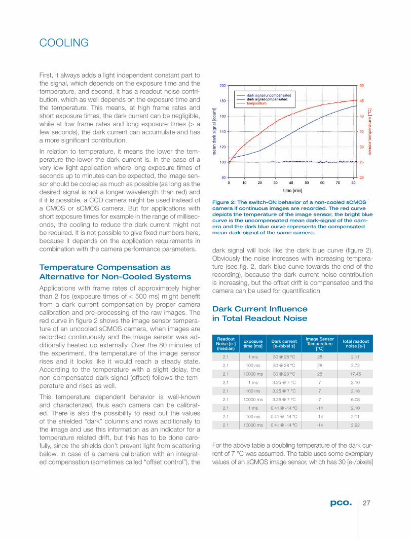
27
COOLING
First, it always adds a light independent constant part to the signal, which depends on the exposure time and the temperature, and second, it has a readout noise contri-bution, which as well depends on the exposure time and the temperature. This means, at high frame rates and short exposure times, the dark current can be negligible, while at low frame rates and long exposure times (> a few seconds), the dark current can accumulate and has a more signifi cant contribution.
In relation to temperature, it means the lower the tem-perature the lower the dark current is. In the case of a very low light application where long exposure times of seconds up to minutes can be expected, the image sen-sor should be cooled as much as possible (as long as the desired signal is not a longer wavelength than red) and if it is possible, a CCD camera might be used instead of a CMOS or sCMOS camera. But for applications with short exposure times for example in the range of millisec-onds, the cooling to reduce the dark current might not be required. It is not possible to give fi xed numbers here, because it depends on the application requirements in combination with the camera performance parameters.
Temperature Compensation asAlternative for Non-Cooled Systems
Applications with frame rates of approximately higher than 2 fps (exposure times of < 500 ms) might benefi t from a dark current compensation by proper camera calibration and pre-processing of the raw images. The red curve in fi gure 2 shows the image sensor tempera-ture of an uncooled sCMOS camera, when images are recorded continuously and the image sensor was ad-ditionally heated up externally. Over the 80 minutes of the experiment, the temperature of the image sensor rises and it looks like it would reach a steady state. According to the temperature with a slight delay, the non-compensated dark signal (offset) follows the tem-perature and rises as well.
This temperature dependent behavior is well-known and characterized, thus each camera can be calibrat-ed. There is also the possibility to read out the values of the shielded “dark” columns and rows additionally to the image and use this information as an indicator for a temperature related drift, but this has to be done care-fully, since the shields don’t prevent light from scattering below. In case of a camera calibration with an integrat-ed compensation (sometimes called “offset control”), the
dark signal will look like the dark blue curve (fi gure 2). Obviously the noise increases with increasing tempera-ture (see fi g. 2, dark blue curve towards the end of the recording), because the dark current noise contribution is increasing, but the offset drift is compensated and the camera can be used for quantifi cation.
Dark Current In� uencein Total Readout Noise
Figure 2: The switch-ON behavior of a non-cooled sCMOS camera if continuous images are recorded. The red curve depicts the temperature of the image sensor, the bright blue curve is the uncompensated mean dark-signal of the cam-era and the dark blue curve represents the compensated mean dark-signal of the same camera.
Readout Noise [e-] (median)
Exposure time [ms]
Dark current [e-/pixel s]
Image Sensor Temperature
[°C]
Total readout noise [e-]
2.1 1 ms 30 @ 28 °C 28 2.11
2.1 100 ms 30 @ 28 °C 28 2.72
2.1 10000 ms 30 @ 28 °C 28 17.45
2.1 1 ms 3.25 @ 7 °C 7 2.10
2.1 100 ms 3.25 @ 7 °C 7 2.18
2.1 10000 ms 3.25 @ 7 °C 7 6.08
2.1 1 ms 0.41 @ -14 °C -14 2.10
2.1 100 ms 0.41 @ -14 °C -14 2.11
2.1 10000 ms 0.41 @ -14 °C -14 2.92
For the above table a doubling temperature of the dark cur-rent of 7 °C was assumed. The table uses some exemplary values of an sCMOS image sensor, which has 30 [e-/pixels]
IS IT TRUE THAT COOLED CAMERAS ARE MORE SENSITIVE THAN NON-COOLED CAMERAS?
The temperature has a signifi cant impact on certain noise sources prevalent in cameras, which contribute to the to-tal readout noise of an image sensor. When electronic devices are operated continuously, they dissipate heat due to losses in the signal processing, and reduction of temperature via “cooling” of image sensor components or electronic circuits in devices can indeed improve im-age quality and performance.
Upon further inspection, the advantages and disadvan-tages of cooling reveal that cooled cameras may not necessarily be more sensitive than non-cooled camer-as. For this we need a closer look at the underlying effects of cooling.
Temperature Control
Subsequently, this camera can be used for light intensity quantifi cation, because any change of the signal will be due to incoming light as opposed to fl uctuations in tem-perature. But there is no direct link with the quality of this stabilization and the absolute temperature. Therefore, it is less important to stabilize the image sensor at a deep or low temperature, but rather more critical to stabilize or control it. The drift or signal change in fi gure 1 per hour is about 0.5 [count], which means, it is extremely stable.
Reduction of Dark Current
Another reason for cooling is the reduction of noise. In a light sensitive pixel, there are temperature relat-ed noise sources which can be minimized by cooling. There also remains the possibility of temperature gen-erated charge carriers, called dark current. One of the remaining advantages of CCD image sensors com-pared to CMOS and sCMOS image sensors is the low-er dark current, as the latter always have signifi cantly higher dark current values. The contribution of the dark current to the signal is dependent on the exposure time and the operating temperature. If we have a look to the dark signal µd of an image sensor or camera, there is a temperature independent part µd.0 and the temperature related part µtherm. This goes linearly with the exposure time and equals the dark current µI (unit = [e-/(pixel *s)]) times the exposure time texp:
𝜇𝑑 = 𝜇𝑑.0 + 𝜇therm = 𝜇𝑑.0 + 𝜇𝐼 ⋅ texp1
According to the laws of error propagation, the variance of the dark signal is then given as:
𝜎𝑑2 = 𝜎𝑑
2.0 + 𝜎2
therm = 𝜎𝑑2
.0 + 𝜇𝐼 ⋅ texp
Because the thermally induced electrons are Poisson dis-tributed as are the light induced ones with 𝜎2
therm = 𝜇therm. Therefore the dark current has different consequences.
Figure 1: A four hour measurement of the mean dark signal of an sCMOS camera, which was continuously read out at full speed (100 fps) and whose image sensor was tempera-ture controlled at + 5°C (pco.edge 5.5).
The major reason for cooling is the temperature control of a camera system and especially the image sensor. Fig-ure 1 shows an image sensor that is thermally stabilized with a thermo-electric Peltier-cooler; the camera can be operated, but the offset, the dark value, stays constant.

28
DNA-PAINT: A SUPER-RESOLUTION MICROSCOPY TECHNIQUE
Super-resolution1 techniques have enabled researchers to perform imaging below the classical diffraction-lim-it of light with thus far unprecedented precision. In sin-gle-molecule localization implementations, molecules are 'switched' between non-� uorescent dark- (or OFF-) and � uorescent bright-states (or ON-states) in order to assign and detect their position with sub-diffraction precision. By acquiring not only one, but rather a whole stack of images, in which only a random subset of � uorescent molecules (which differs from frame to frame) are recorded in the “ON-state”, a super-resolved image can be constructed.
The recently introduced super-resolution method DNA-PAINT2 is based on transient DNA-DNA interactions. Compared to other stochastic approaches such as STORM3, PALM4, or GSDIM5 the � uorescence molecules aren’t switched between dark and bright states, but the so-called “blinking” in DNA-PAINT is created by transient hybridization (binding and unbinding) of short � uorescent DNA strands (imagers) to their targets (� gure 1a). Once the imager is bound to the docking site, the � uorophore is immobilized and can be detected by a camera. DNA-PAINT does not suffer from photobleaching as the imag-er strands are dynamically replenished. This allows the extraction of the full photon capacity of an immobilized imager strand upon binding to the docking site, facili-tating superior resolution down to a few nanometers6. The high signal-to-background ratio enables the com-bination of DNA-PAINT and confocal approaches, such as spinning disc confocal microscopy7. We assayed a new non-cooled scienti� c CMOS camera (pco.panda 4.2) with synthetic DNA nanostructures. Therefore, we decorated a � at rectangle DNA origami with DNA-PAINT docking sites in a grid pattern with 10 nm spacing (� gure 1b) and imaged the surface-bound structures using total internal re� ection � uorescence8 (TIRF) microscopy. Indi-vidual docking sites could be localized with a precision of around 1.5 nm, translating to a remarkable FWHM-reso-lution ~3.6 nm (Figure 1c).
Due to the programmable nature DNA interactions in DNA-PAINT, multicolor image acquisition is not limited to spectral multiplexing. The DNA sequence of the imager strand can serve as a pseudo-color, where every orthog-onal sequence represents a unique color. This enables multiplexed imaging using the same best-performing � uorescent dye, in a method called exchange-PAINT9. Image acquisition is then performed sequentially. The transiently binding imager strands can be removed using washing buffer and the new ‘color’ (e.g. imagers with a different sequence) can be introduced.
Figure 1: DNA-PAINT imaging of DNA origami. (a) DNA-PAINT principle: Short oligonucleotides functionalized with � uores-cent dyes bind transiently to complementary DNA strands (docking site) localized at the target. (b) Flat rectangle DNA origami decorated for DNA-PAINT imaging with a 4 x 4 grid pattern, spacing 10 nm. (c) Sum image of n = 24 DNA origa-mi imaged with DNA-PAINT and the sCMOS camera (pco.panda 4.2). Scale bar: 20 nm (a).
By Alexander Auer & Ralf Jungmann
COOLING
dark current at 21 °C temperature. A reduction of the tem-perature by 7 °C means half of the dark current. The total readout noise, which determines the achievable signal-to-noise-ratio, changes then according to exposure time and temperature of the image sensor. There are three different exposure times assumed: 1 ms – 100 ms – 10000 ms to show the contribution of the dark current to the total readout noise, and all this is given at different image sensor tempera-tures from 28 °C via 7 °C down to – 14 °C. Clearly for the long exposure time of 10 s and the high sensor temperature the additional noise contribution is much too high, but at 100 ms exposure time the dark current related increase of 0.6 [e-] of the total readout noise is reasonable, and at 1 ms exposure time, the dark current has no impact. If the image sensor is cooled down to – 14 °C even the 10 s exposure time can be used, because the readout noise increase of 0.82 [e-] is acceptable.
The table shows for these performance data, the image sen-sor can be used at 28 °C for exposure times of 100 ms and shorter. If, for the given example, the image sensor should be used at exposure times of 10 s, a cooling of the image sensor for example down to – 14 °C would be required.
Disadvantage of Cooling
An intriguing relationship of temperature and image sensor behavior exists, likely attributable to the pure semi-conductor physics of silicon. Measuring light with-in an integrating sphere and with homogenous illumina-tion at different image sensor temperatures and differ-ent wavelengths produces unexpected and somewhat surprising results. The results in � gure 3 show the tem-perature dependence of the relative quantum ef� ciency for various wavelengths. The signals are all related to the values of the camera when the image sensor has a temperature of + 5°C. Similar results have been obtained with CCD image sensors.
From UV to green radiation, the sensitivity of the image sensor increases a little with cooling, but only 1-2 %. Red to NIR produces the opposite effect, where the more the image sensor is cooled the less sensitive it becomes for this spectral range of radiation. For example, for a wave-length of λ = 950 nm the loss of relative quantum ef� -ciency with a cooling from +5 °C down to -25 °C is 18 %. In turn this means using a deep cooled camera (- 50 °C sensor temperature) to measure long wavelength radia-tion (> 700 nm) is not optimal.
Cooling reduces the mobility of the charge carriers, and for long wavelength detection the radiation is penetrat-ing deep into the silicon to be able to generate a charge carrier (electron-hole pair). Now the charge carrier has to drift a large distance, and it does it slower, which increas-es the probability that it either recombines or gets lost by other mechanisms, but it doesn’t contribute to the signal. For sure this effect has to be balanced with the tempera-ture induced dark current noise contribution.
So, Are Cooled CamerasMore Sensitive?
No, not in general! As described, the cooling reduces the readout noise in some situations, and is recommended for longer exposure times (many seconds to minutes), but it also might have a negative effect on the quantum ef� ciency. Thermal stabilization is a good thing in general, but, in case proper calibration and compensation is con-ducted, it is not always required.
Figure 3: Measurement of the relative quantum ef� ciency of an sCMOS image sensor taken at different image sensor temperatures for various wavelengths (378 nm – 451 nm – 516 nm – 643 nm – 740 nm – 950 nm).
END NOTES
1 Equation 19 from EMVA 1288 Standard - Standard for Characterization of Image Sensors and Cameras, Release 3.1

29
DNA-PAINT: A SUPER-RESOLUTION MICROSCOPY TECHNIQUE
Super-resolution1 techniques have enabled researchers to perform imaging below the classical diffraction-lim-it of light with thus far unprecedented precision. In sin-gle-molecule localization implementations, molecules are 'switched' between non-� uorescent dark- (or OFF-) and � uorescent bright-states (or ON-states) in order to assign and detect their position with sub-diffraction precision. By acquiring not only one, but rather a whole stack of images, in which only a random subset of � uorescent molecules (which differs from frame to frame) are recorded in the “ON-state”, a super-resolved image can be constructed.
The recently introduced super-resolution method DNA-PAINT2 is based on transient DNA-DNA interactions. Compared to other stochastic approaches such as STORM3, PALM4, or GSDIM5 the � uorescence molecules aren’t switched between dark and bright states, but the so-called “blinking” in DNA-PAINT is created by transient hybridization (binding and unbinding) of short � uorescent DNA strands (imagers) to their targets (� gure 1a). Once the imager is bound to the docking site, the � uorophore is immobilized and can be detected by a camera. DNA-PAINT does not suffer from photobleaching as the imag-er strands are dynamically replenished. This allows the extraction of the full photon capacity of an immobilized imager strand upon binding to the docking site, facili-tating superior resolution down to a few nanometers6. The high signal-to-background ratio enables the com-bination of DNA-PAINT and confocal approaches, such as spinning disc confocal microscopy7. We assayed a new non-cooled scienti� c CMOS camera (pco.panda 4.2) with synthetic DNA nanostructures. Therefore, we decorated a � at rectangle DNA origami with DNA-PAINT docking sites in a grid pattern with 10 nm spacing (� gure 1b) and imaged the surface-bound structures using total internal re� ection � uorescence8 (TIRF) microscopy. Indi-vidual docking sites could be localized with a precision of around 1.5 nm, translating to a remarkable FWHM-reso-lution ~3.6 nm (Figure 1c).
Due to the programmable nature DNA interactions in DNA-PAINT, multicolor image acquisition is not limited to spectral multiplexing. The DNA sequence of the imager strand can serve as a pseudo-color, where every orthog-onal sequence represents a unique color. This enables multiplexed imaging using the same best-performing � uorescent dye, in a method called exchange-PAINT9. Image acquisition is then performed sequentially. The transiently binding imager strands can be removed using washing buffer and the new ‘color’ (e.g. imagers with a different sequence) can be introduced.
Figure 1: DNA-PAINT imaging of DNA origami. (a) DNA-PAINT principle: Short oligonucleotides functionalized with � uores-cent dyes bind transiently to complementary DNA strands (docking site) localized at the target. (b) Flat rectangle DNA origami decorated for DNA-PAINT imaging with a 4 x 4 grid pattern, spacing 10 nm. (c) Sum image of n = 24 DNA origa-mi imaged with DNA-PAINT and the sCMOS camera (pco.panda 4.2). Scale bar: 20 nm (a).
By Alexander Auer & Ralf Jungmann
COOLING
dark current at 21 °C temperature. A reduction of the tem-perature by 7 °C means half of the dark current. The total readout noise, which determines the achievable signal-to-noise-ratio, changes then according to exposure time and temperature of the image sensor. There are three different exposure times assumed: 1 ms – 100 ms – 10000 ms to show the contribution of the dark current to the total readout noise, and all this is given at different image sensor tempera-tures from 28 °C via 7 °C down to – 14 °C. Clearly for the long exposure time of 10 s and the high sensor temperature the additional noise contribution is much too high, but at 100 ms exposure time the dark current related increase of 0.6 [e-] of the total readout noise is reasonable, and at 1 ms exposure time, the dark current has no impact. If the image sensor is cooled down to – 14 °C even the 10 s exposure time can be used, because the readout noise increase of 0.82 [e-] is acceptable.
The table shows for these performance data, the image sen-sor can be used at 28 °C for exposure times of 100 ms and shorter. If, for the given example, the image sensor should be used at exposure times of 10 s, a cooling of the image sensor for example down to – 14 °C would be required.
Disadvantage of Cooling
An intriguing relationship of temperature and image sensor behavior exists, likely attributable to the pure semi-conductor physics of silicon. Measuring light with-in an integrating sphere and with homogenous illumina-tion at different image sensor temperatures and differ-ent wavelengths produces unexpected and somewhat surprising results. The results in � gure 3 show the tem-perature dependence of the relative quantum ef� ciency for various wavelengths. The signals are all related to the values of the camera when the image sensor has a temperature of + 5°C. Similar results have been obtained with CCD image sensors.
From UV to green radiation, the sensitivity of the image sensor increases a little with cooling, but only 1-2 %. Red to NIR produces the opposite effect, where the more the image sensor is cooled the less sensitive it becomes for this spectral range of radiation. For example, for a wave-length of λ = 950 nm the loss of relative quantum ef� -ciency with a cooling from +5 °C down to -25 °C is 18 %. In turn this means using a deep cooled camera (- 50 °C sensor temperature) to measure long wavelength radia-tion (> 700 nm) is not optimal.
Cooling reduces the mobility of the charge carriers, and for long wavelength detection the radiation is penetrat-ing deep into the silicon to be able to generate a charge carrier (electron-hole pair). Now the charge carrier has to drift a large distance, and it does it slower, which increas-es the probability that it either recombines or gets lost by other mechanisms, but it doesn’t contribute to the signal. For sure this effect has to be balanced with the tempera-ture induced dark current noise contribution.
So, Are Cooled CamerasMore Sensitive?
No, not in general! As described, the cooling reduces the readout noise in some situations, and is recommended for longer exposure times (many seconds to minutes), but it also might have a negative effect on the quantum ef� ciency. Thermal stabilization is a good thing in general, but, in case proper calibration and compensation is con-ducted, it is not always required.
Figure 3: Measurement of the relative quantum ef� ciency of an sCMOS image sensor taken at different image sensor temperatures for various wavelengths (378 nm – 451 nm – 516 nm – 643 nm – 740 nm – 950 nm).
END NOTES
1 Equation 19 from EMVA 1288 Standard - Standard for Characterization of Image Sensors and Cameras, Release 3.1

30
APPLICATION DNA-PAINT
To image cellular components with DNA-PAINT, label-ing probes (for example antibodies10, nanobodies11 or Affi mers12) were conjugated with short DNA oligonucle-otides serving as the docking site. We investigated the imaging capability of a non-cooled sCMOS camera in a cellular environment of a fi xed COS7 cell, where alpha tubulin was labeled with primary and secondary antibody (fi gure 2). The overview (fi gure 2a) shows the super-re-solved microtubule network. Comparison of the diffrac-tion-limited zoom-in panel in fi gure 2b with the super-re-solved zoom-in fi gure 2c clearly displays the increase in resolution, allowing the discrimination and the distance measurement (fi gure 2d) between individual tubulin fi la-ments. Clearly a non-cooled sCMOS camera is well suit-ed to do these kind of super resolution measurements with the DNA-PAINT method.
Figure 2: DNA-PAINT imaging in a cellular environment. (a) Microtubules are labeled with alpha tubulin primary antibod-ies and DNA-conjugated secondary antibodies. Imaging was performed in TIRF mode with an uncooled sCMOS camera (pco.panda 4.2). (b) Diffraction-limited (DL) representation and (c) super-resolution (SR) zoom-in of the highlighted area in a. (d) Cross-sectional histogram of the area marked in (c) shows the distances between three microtubule � laments. Scale bars: 5 µm (a), 500 nm (b, c).
END NOTES
1 Hell, S.W., et al., The 2015 super-resolution microscopy roadmap. Journal of Physics D-Applied Physics, 2015. 48(44).
2 Jungmann, R., et al., Single-molecule kinetics and super-resolution microscopy by fl uorescence imaging of transient binding on DNA origami. Nano Lett, 2010. 10(11): p. 4756-61.
3 Rust, M.J., M. Bates, and X.W. Zhuang, Sub-diffraction-limit imaging by stochastic optical reconstruction microscopy (STORM). Nature Methods, 2006. 3(10): p. 793-795.
4 Betzig, E., et al., Imaging intracellular fl uorescent proteins at nanometer resolu-tion. Science, 2006. 313(5793): p. 1642-1645.
5 Fölling, J., et al., Fluorescence nanoscopy by ground-state depletion and sin-gle-molecule return. Nat Methods 5 (2008), p. 943-945.
6 Dai, M., DNA-PAINT Super-Resolution Imaging for Nucleic Acid Nanostructures. Methods Mol Biol, 2017. 1500: p. 185-202.
7 Schueder, F., et al., Multiplexed 3D super-resolution imaging of whole cells using spinning disk confocal microscopy and DNA-PAINT. Nat Commun, 2017. 8(1): p. 2090.
8 Axelrod, D., Cell-substrate contacts illuminated by total internal refl ection fl uores-cence. J Cell Biol, 1981. 89(1): p. 141-5.
9 Jungmann, R., et al., Multiplexed 3D cellular super-resolution imaging with DNA-PAINT and Exchange-PAINT. Nat Methods, 2014. 11(3): p. 313-8.
10 Schnitzbauer, J., et al., Super-resolution microscopy with DNA-PAINT. Nat Protoc, 2017. 12(6): p. 1198-1228.
11 Agasti, S.S., et al., DNA-barcoded labeling probes for highly multiplexed Ex-change-PAINT imaging. Chem Sci, 2017. 8(4): p. 3080-3091.
12 Schlichthaerle, T., et al., Site-specifi c labeling of Affi mers for DNA-PAINT micros-copy. Angew Chem Int Ed Engl, 2018.
STANDARDS ALWAYSSOUND IMPRESSIVE,BUT IS THERE ANY BENEFIT FOR ME AS AN sCMOS CAMERA USER?
In the case of the EMVA1288, which is a standard for the specifi cation and measurement of machine vision sen-sors and cameras, the answer is – YES, there is a signif-icant benefi t for an sCMOS camera user.
This standard was initiated by the European Machine Vision Association (EMVA)1. The initiative was launched to defi ne a unifi ed method to measure, compute and present specifi cation parameters for cameras and image sensors used for machine vision applications, but it is not limited to machine vision applications. It has also been further accepted by the American Automated Imaging Association (AIA)2 and the Japan Industrial Imaging As-sociation (JIIA)3.
What is the reason for theEMVA1288 standard?
Choosing a suitable camera for a given imaging appli-cation often proves to be a challenging task. The data sheets provided by the manufacturers are diffi cult to compare. Frequently, vital pieces of information are not available and the user is forced to conduct a costly comparative test which still may fail to deliver all rele-vant camera parameters. This is where the EMVA 1288 Standard comes in. It creates transparency by defi ning reliable and exact measurement procedures as well as
data presentation guidelines and makes the comparison of cameras and image sensors much easier.
The Standard is elaborated by a consortium of the in-dustry leading sensor and camera manufacturers, dis-tributers and component customers4. The Standard is organized in a modular approach. The fi rst module was offi cially released by the working group member compa-nies in August 2005.
The EMVA1288 standard is continuously improved and missing topics are integrated. To understand how the information is presented and prepared for customers, it is relevant to have a look to the summary sheet of a digital camera.
The summary data sheet as shown in fi gure 1 contains three mayor elements.
[1] Operating point: Contains a complete description of the settings of the operating point at which the EMVA 1288 measurements have been acquired. Settings not specifi ed are assumed to be in the factory default mode. If, for instance, the binning factor is not given, the camera was measured without binning. This en-sures that the measurements can be repeated any-time under the same conditions.
[2] Photon transfer and SNR curves: The upper graph contains the photon transfer curve [2a], i.e., the vari-ance of the image sensor noise versus the mean value. For an ideal linear camera this curve should be linear. Only if the lower 70 % of the curve is lin-ear, can the EMVA 1288 performance parameters be estimated accurately. If a camera has any type of defi ciencies, these can often fi rst be seen in the

31
APPLICATION DNA-PAINT
To image cellular components with DNA-PAINT, label-ing probes (for example antibodies10, nanobodies11 or Affi mers12) were conjugated with short DNA oligonucle-otides serving as the docking site. We investigated the imaging capability of a non-cooled sCMOS camera in a cellular environment of a fi xed COS7 cell, where alpha tubulin was labeled with primary and secondary antibody (fi gure 2). The overview (fi gure 2a) shows the super-re-solved microtubule network. Comparison of the diffrac-tion-limited zoom-in panel in fi gure 2b with the super-re-solved zoom-in fi gure 2c clearly displays the increase in resolution, allowing the discrimination and the distance measurement (fi gure 2d) between individual tubulin fi la-ments. Clearly a non-cooled sCMOS camera is well suit-ed to do these kind of super resolution measurements with the DNA-PAINT method.
Figure 2: DNA-PAINT imaging in a cellular environment. (a) Microtubules are labeled with alpha tubulin primary antibod-ies and DNA-conjugated secondary antibodies. Imaging was performed in TIRF mode with an uncooled sCMOS camera (pco.panda 4.2). (b) Diffraction-limited (DL) representation and (c) super-resolution (SR) zoom-in of the highlighted area in a. (d) Cross-sectional histogram of the area marked in (c) shows the distances between three microtubule � laments. Scale bars: 5 µm (a), 500 nm (b, c).
END NOTES
1 Hell, S.W., et al., The 2015 super-resolution microscopy roadmap. Journal of Physics D-Applied Physics, 2015. 48(44).
2 Jungmann, R., et al., Single-molecule kinetics and super-resolution microscopy by fl uorescence imaging of transient binding on DNA origami. Nano Lett, 2010. 10(11): p. 4756-61.
3 Rust, M.J., M. Bates, and X.W. Zhuang, Sub-diffraction-limit imaging by stochastic optical reconstruction microscopy (STORM). Nature Methods, 2006. 3(10): p. 793-795.
4 Betzig, E., et al., Imaging intracellular fl uorescent proteins at nanometer resolu-tion. Science, 2006. 313(5793): p. 1642-1645.
5 Fölling, J., et al., Fluorescence nanoscopy by ground-state depletion and sin-gle-molecule return. Nat Methods 5 (2008), p. 943-945.
6 Dai, M., DNA-PAINT Super-Resolution Imaging for Nucleic Acid Nanostructures. Methods Mol Biol, 2017. 1500: p. 185-202.
7 Schueder, F., et al., Multiplexed 3D super-resolution imaging of whole cells using spinning disk confocal microscopy and DNA-PAINT. Nat Commun, 2017. 8(1): p. 2090.
8 Axelrod, D., Cell-substrate contacts illuminated by total internal refl ection fl uores-cence. J Cell Biol, 1981. 89(1): p. 141-5.
9 Jungmann, R., et al., Multiplexed 3D cellular super-resolution imaging with DNA-PAINT and Exchange-PAINT. Nat Methods, 2014. 11(3): p. 313-8.
10 Schnitzbauer, J., et al., Super-resolution microscopy with DNA-PAINT. Nat Protoc, 2017. 12(6): p. 1198-1228.
11 Agasti, S.S., et al., DNA-barcoded labeling probes for highly multiplexed Ex-change-PAINT imaging. Chem Sci, 2017. 8(4): p. 3080-3091.
12 Schlichthaerle, T., et al., Site-specifi c labeling of Affi mers for DNA-PAINT micros-copy. Angew Chem Int Ed Engl, 2018.
STANDARDS ALWAYSSOUND IMPRESSIVE,BUT IS THERE ANY BENEFIT FOR ME AS AN sCMOS CAMERA USER?
In the case of the EMVA1288, which is a standard for the specifi cation and measurement of machine vision sen-sors and cameras, the answer is – YES, there is a signif-icant benefi t for an sCMOS camera user.
This standard was initiated by the European Machine Vision Association (EMVA)1. The initiative was launched to defi ne a unifi ed method to measure, compute and present specifi cation parameters for cameras and image sensors used for machine vision applications, but it is not limited to machine vision applications. It has also been further accepted by the American Automated Imaging Association (AIA)2 and the Japan Industrial Imaging As-sociation (JIIA)3.
What is the reason for theEMVA1288 standard?
Choosing a suitable camera for a given imaging appli-cation often proves to be a challenging task. The data sheets provided by the manufacturers are diffi cult to compare. Frequently, vital pieces of information are not available and the user is forced to conduct a costly comparative test which still may fail to deliver all rele-vant camera parameters. This is where the EMVA 1288 Standard comes in. It creates transparency by defi ning reliable and exact measurement procedures as well as
data presentation guidelines and makes the comparison of cameras and image sensors much easier.
The Standard is elaborated by a consortium of the in-dustry leading sensor and camera manufacturers, dis-tributers and component customers4. The Standard is organized in a modular approach. The fi rst module was offi cially released by the working group member compa-nies in August 2005.
The EMVA1288 standard is continuously improved and missing topics are integrated. To understand how the information is presented and prepared for customers, it is relevant to have a look to the summary sheet of a digital camera.
The summary data sheet as shown in fi gure 1 contains three mayor elements.
[1] Operating point: Contains a complete description of the settings of the operating point at which the EMVA 1288 measurements have been acquired. Settings not specifi ed are assumed to be in the factory default mode. If, for instance, the binning factor is not given, the camera was measured without binning. This en-sures that the measurements can be repeated any-time under the same conditions.
[2] Photon transfer and SNR curves: The upper graph contains the photon transfer curve [2a], i.e., the vari-ance of the image sensor noise versus the mean value. For an ideal linear camera this curve should be linear. Only if the lower 70 % of the curve is lin-ear, can the EMVA 1288 performance parameters be estimated accurately. If a camera has any type of defi ciencies, these can often fi rst be seen in the

32
photon transfer curve. The double-logarithmic SNR curve [2b] is a nice overall graphical representation of all camera performance parameters except for the dark current. The absolute sensitivity threshold is marked as well as the saturation capacity. In addi-tion, the maximum signal-to-noise ratio and the dy-namic range can be read from the graph. The total SNR is plotted as a dashed line. It includes both the variances from the temporal noise and the nonuni-formities. If this line lies recognizably below the solid line of the SNR curve, nonuniformities signifi cantly reduce the performance of the camera.
[3] EMVA 1288 performance parameters: This col-umn lists all EMVA 1288 performance parameters.Here only some aspects of the three most important are discussed:
[3a] Quantum effi ciency: Denotes how effi ciently a camera converts light into electric charges. Thus, if you have enough light in your applica-tion, this parameter is not critical. Be aware that this parameter requires an absolute calibration of the measuring equipment which is typically not more accurate than 3 %. So differences in the quantum effi ciencies between different data sheets in the range of a few percent are not sig-nifi cant and not decision criterion.
[3b] Absolute sensitivity threshold: Tells you the low-est light level the camera can detect. It is given in photons and in photons per area unit (μm²). The latter is important if you compare cameras with different pixel sizes because in most applications the irradiance (photons per time and area) at the image plane is given.
[3c] Saturation capacity: Gives the largest irradiation the camera can measure. It also determines the best possible signal quality you can get from an image sensor, the maximum signal-to-noise ratio.
These exemplary considerations clearly indicate how you can fi nd the best camera for your application. Find out the most critical parameter by asking questions like: Do I have enough light? Do I have to see both dark and bright parts in the image with enough resolution? Do I have to detect slight intensity variations? Then take the corre-sponding EMVA 1288 parameters and compare.
Bene� t for sCMOS camera users
In case an sCMOS camera should be selected for a sci-entifi c application, the customer can ask the manufac-turers for an EMVA1288 compliant data sheet, because these data sheets are at the moment the best possible way to compare the performance data of the variety of available sCMOS cameras prior to an application. How-ever, a demo testing will always give the fi nal arguments for the correct camera system decision.
END NOTES
1 https://www.emva.org/
2 https://www.visiononline.org/
3 http://jiia.org/en/
4 https://www.emva.org/standards-technology/emva-1288/
EMVA 1288 TEST STANDARDS
Figure 1: The EMVA1288 summary sheet of a CMOS camera.
EMVA 1288 TEST STANDARDS

33
photon transfer curve. The double-logarithmic SNR curve [2b] is a nice overall graphical representation of all camera performance parameters except for the dark current. The absolute sensitivity threshold is marked as well as the saturation capacity. In addi-tion, the maximum signal-to-noise ratio and the dy-namic range can be read from the graph. The total SNR is plotted as a dashed line. It includes both the variances from the temporal noise and the nonuni-formities. If this line lies recognizably below the solid line of the SNR curve, nonuniformities signifi cantly reduce the performance of the camera.
[3] EMVA 1288 performance parameters: This col-umn lists all EMVA 1288 performance parameters.Here only some aspects of the three most important are discussed:
[3a] Quantum effi ciency: Denotes how effi ciently a camera converts light into electric charges. Thus, if you have enough light in your applica-tion, this parameter is not critical. Be aware that this parameter requires an absolute calibration of the measuring equipment which is typically not more accurate than 3 %. So differences in the quantum effi ciencies between different data sheets in the range of a few percent are not sig-nifi cant and not decision criterion.
[3b] Absolute sensitivity threshold: Tells you the low-est light level the camera can detect. It is given in photons and in photons per area unit (μm²). The latter is important if you compare cameras with different pixel sizes because in most applications the irradiance (photons per time and area) at the image plane is given.
[3c] Saturation capacity: Gives the largest irradiation the camera can measure. It also determines the best possible signal quality you can get from an image sensor, the maximum signal-to-noise ratio.
These exemplary considerations clearly indicate how you can fi nd the best camera for your application. Find out the most critical parameter by asking questions like: Do I have enough light? Do I have to see both dark and bright parts in the image with enough resolution? Do I have to detect slight intensity variations? Then take the corre-sponding EMVA 1288 parameters and compare.
Bene� t for sCMOS camera users
In case an sCMOS camera should be selected for a sci-entifi c application, the customer can ask the manufac-turers for an EMVA1288 compliant data sheet, because these data sheets are at the moment the best possible way to compare the performance data of the variety of available sCMOS cameras prior to an application. How-ever, a demo testing will always give the fi nal arguments for the correct camera system decision.
END NOTES
1 https://www.emva.org/
2 https://www.visiononline.org/
3 http://jiia.org/en/
4 https://www.emva.org/standards-technology/emva-1288/
EMVA 1288 TEST STANDARDS
Figure 1: The EMVA1288 summary sheet of a CMOS camera.
EMVA 1288 TEST STANDARDS

34
WHY IS A BACKSIDE ILLUMINATED SENSORMORE SENSITIVE THANA FRONT SIDE ILLUMINATED?
All image sensors have light sensitive pixels, but what does that mean? The pixels allow a spatial localization of incoming light and consist of various electronics in-terconnected with metal wires to enable digitization. The basic light to charge carrier conversion elements are the photodiodes (fi gure 2). Both the lateral area and volume of a pixel are shared by photodiodes, metal wiring, tran-sistors and capacitors. Thus, the sensitivity of an image sensor strongly depends on how much of the total pixel area is used for light to charge carrier conversion, or in other words, is light sensitive.
Fill Factor
The fi ll factor is a technical term for an image sensor which describes the ratio of light sensitive area to total area of a pixel:
fill factor = light sensitive area of pixel
total area of pixel
For example, in interline transfer CCD image sensors where the pixel area was shared by the photodiode and the shield-ed register, the fi ll factor was in the range of 30 %. This means, a minimum of 70 % of the incoming light would have been lost. The same principle holds true for CMOS image sensors, where all the transistors, capacitors and wires oc-cupy valuable light converting space (fi gure 1).
Figure 1 depicts the pixel layout of a CMOS image sen-sor with 6 transistors in each pixel and a fi ll factor of approximately 50 %. During CCD sensor development, measures were developed to compensate the fi ll factor loss. The most effective measure was done simply by adding micro lenses on top of the image sensor. Figure
2 illustrates the differences in light collection shown for perpendicular impinging light. While some of the light is scattered, refl ected or absorbed in spaces of the image sensors, the microlenses focus the light to the charge conversion photodiodes much more effi ciently than without (fi gure 2a and 2b).
By this measure, the CMOS image sensor, shown in fi g-ure 1 has a total quantum effi ciency of about 50 % - quite good considering there are additional loss mechanisms in image sensors. The best quantum effi ciencies achieved
Figure 1: Pixel Layout of a CMOS image sensor with 50 %� ll factor (3x3 pixels shown).
BACKSIDE ILLUMINATION
in interline transfer CCDs (with 30 % fi ll factor) have been around 50 to 70 %. In more recent sCMOS image sensors with similar fi ll factors, quantum effi ciencies of above 80 % have been achieved by optimization of the micro-lenses and the manufacturing process. But the micro-lenses are, in most cases, made of moldable plastic material, which attenuates signifi cantly any UV light transmission.
Furthermore, there is a new infl uence introduced by micro lenses, since the performance of these optical devices is dependent on the angle of incidence. This means that the micro lenses add a more pronounced angular dependency to the quantum effi ciency, as can be seen in fi gure 3.
signifi cantly, while the vertical dependence is less pro-nounced, which can be explained by the fact that in vertical direction the light sensitive area nearly covers the whole pixel while horizontally half or more of the area is used by the shielded register.
From Frontside to Backside Illumination
However, the micro-lenses cannot collect and focus all ray angles of incoming light. Further, the semiconduc-tor manufacturing process contributes additional layers above the photodiodes (fi gure 4, depicting the wiring, the transistors and the capacitors). The electronics in these layers can cause light to be scattered and absorbed, re-sulting in a loss of light to charge conversion.
Metal Wiring
Substrate
Photodiodes
Metal Wiring
Metal Wiring
Substrate
On-Chip Lens
Photodiodes
Metal Wiring
Figure 2: Schematic cross section through a frontside illuminated CMOS image sensor without (a) and with micro lenses (b) to illustrate the micro lens effect of improving the light collection.
Figure 3: Measured data of the vertical and horizontalangular dependence of the relative quantum ef� ciencyof a interline transfer CCD (KAI-2020) with micro lenses.
The blue curve shows the horizontal angular depen-dence of the relative quantum effi ciency of the interline transfer CCD image sensor. From an incident angle of 5 ° and higher, the relative quantum effi ciency drops
Metal Wiring
Substrate
On-Chip Lens
Photodiodes
Metal Wiring
Metal Wiring
On-Chip Lens
Photodiodes
Metal Wiring
Frontside Illuminated Image Sensor Backside Illuminated Image Sensor
Figure 4: Schematic cross section through a frontside illumi-nated CMOS image sensor with micro lenses (a) and a back-side illuminated CMOS image sensor with micro lenses (b) to illustrate the effect of frontside vs. backside illumination.
The loss of light due to physical blocking and scatter-ing by electronics is more pronounced in CMOS image sensors with small pixel pitches and higher pixel counts (> 4 MPixel) than many CCD sensors. Due to massive adoption of CMOS sensors (e.g. smart phone cameras) semiconductor manufacturers have developed methods to process the wafer with the image sensors effectively reversed, and a large part of the substrates physically and chemically etched away. This process results in image sensors that are effectively illuminated from the back, and the light reaches the photodiodes more directly (fi gure 4b).
Backside illumination of current CMOS image sensors has seen quantum effi ciencies better than 90 %. By the introduction of an additional surface (the surface of the backside), there are also additional dark current and noise sources added, the caveat being that many back-side illuminated image sensors have higher dark current compared to the frontside illuminated counterparts.

35
WHY IS A BACKSIDE ILLUMINATED SENSORMORE SENSITIVE THANA FRONT SIDE ILLUMINATED?
All image sensors have light sensitive pixels, but what does that mean? The pixels allow a spatial localization of incoming light and consist of various electronics in-terconnected with metal wires to enable digitization. The basic light to charge carrier conversion elements are the photodiodes (fi gure 2). Both the lateral area and volume of a pixel are shared by photodiodes, metal wiring, tran-sistors and capacitors. Thus, the sensitivity of an image sensor strongly depends on how much of the total pixel area is used for light to charge carrier conversion, or in other words, is light sensitive.
Fill Factor
The fi ll factor is a technical term for an image sensor which describes the ratio of light sensitive area to total area of a pixel:
fill factor = light sensitive area of pixel
total area of pixel
For example, in interline transfer CCD image sensors where the pixel area was shared by the photodiode and the shield-ed register, the fi ll factor was in the range of 30 %. This means, a minimum of 70 % of the incoming light would have been lost. The same principle holds true for CMOS image sensors, where all the transistors, capacitors and wires oc-cupy valuable light converting space (fi gure 1).
Figure 1 depicts the pixel layout of a CMOS image sen-sor with 6 transistors in each pixel and a fi ll factor of approximately 50 %. During CCD sensor development, measures were developed to compensate the fi ll factor loss. The most effective measure was done simply by adding micro lenses on top of the image sensor. Figure
2 illustrates the differences in light collection shown for perpendicular impinging light. While some of the light is scattered, refl ected or absorbed in spaces of the image sensors, the microlenses focus the light to the charge conversion photodiodes much more effi ciently than without (fi gure 2a and 2b).
By this measure, the CMOS image sensor, shown in fi g-ure 1 has a total quantum effi ciency of about 50 % - quite good considering there are additional loss mechanisms in image sensors. The best quantum effi ciencies achieved
Figure 1: Pixel Layout of a CMOS image sensor with 50 %� ll factor (3x3 pixels shown).
BACKSIDE ILLUMINATION
in interline transfer CCDs (with 30 % fi ll factor) have been around 50 to 70 %. In more recent sCMOS image sensors with similar fi ll factors, quantum effi ciencies of above 80 % have been achieved by optimization of the micro-lenses and the manufacturing process. But the micro-lenses are, in most cases, made of moldable plastic material, which attenuates signifi cantly any UV light transmission.
Furthermore, there is a new infl uence introduced by micro lenses, since the performance of these optical devices is dependent on the angle of incidence. This means that the micro lenses add a more pronounced angular dependency to the quantum effi ciency, as can be seen in fi gure 3.
signifi cantly, while the vertical dependence is less pro-nounced, which can be explained by the fact that in vertical direction the light sensitive area nearly covers the whole pixel while horizontally half or more of the area is used by the shielded register.
From Frontside to Backside Illumination
However, the micro-lenses cannot collect and focus all ray angles of incoming light. Further, the semiconduc-tor manufacturing process contributes additional layers above the photodiodes (fi gure 4, depicting the wiring, the transistors and the capacitors). The electronics in these layers can cause light to be scattered and absorbed, re-sulting in a loss of light to charge conversion.
Metal Wiring
Substrate
Photodiodes
Metal Wiring
Metal Wiring
Substrate
On-Chip Lens
Photodiodes
Metal Wiring
Figure 2: Schematic cross section through a frontside illuminated CMOS image sensor without (a) and with micro lenses (b) to illustrate the micro lens effect of improving the light collection.
Figure 3: Measured data of the vertical and horizontalangular dependence of the relative quantum ef� ciencyof a interline transfer CCD (KAI-2020) with micro lenses.
The blue curve shows the horizontal angular depen-dence of the relative quantum effi ciency of the interline transfer CCD image sensor. From an incident angle of 5 ° and higher, the relative quantum effi ciency drops
Metal Wiring
Substrate
On-Chip Lens
Photodiodes
Metal Wiring
Metal Wiring
On-Chip Lens
Photodiodes
Metal Wiring
Frontside Illuminated Image Sensor Backside Illuminated Image Sensor
Figure 4: Schematic cross section through a frontside illumi-nated CMOS image sensor with micro lenses (a) and a back-side illuminated CMOS image sensor with micro lenses (b) to illustrate the effect of frontside vs. backside illumination.
The loss of light due to physical blocking and scatter-ing by electronics is more pronounced in CMOS image sensors with small pixel pitches and higher pixel counts (> 4 MPixel) than many CCD sensors. Due to massive adoption of CMOS sensors (e.g. smart phone cameras) semiconductor manufacturers have developed methods to process the wafer with the image sensors effectively reversed, and a large part of the substrates physically and chemically etched away. This process results in image sensors that are effectively illuminated from the back, and the light reaches the photodiodes more directly (fi gure 4b).
Backside illumination of current CMOS image sensors has seen quantum effi ciencies better than 90 %. By the introduction of an additional surface (the surface of the backside), there are also additional dark current and noise sources added, the caveat being that many back-side illuminated image sensors have higher dark current compared to the frontside illuminated counterparts.

36
Backside Illuminated Image sensors with Micro-Lenses?
The advantage of having fewer layers above the photo-diodes (higher sensitivity) also presents a disadvantage in decreased sharpness, or spatial resolution (techni-cally measured as modulation transfer function (MTF)). Due to the remaining substrate above the photodiodes, backside illuminated image sensors generally show a decreased MTF, and if light arrives at particular angles, can be scattered or incorrectly guided to the next pixel. Luckily, the same micro-lens method, initially developed to increase the � ll factor, now improves the MTF.
Metal Wiring
On-Chip Lens
Photodiodes
Metal Wiring
Metal Wiring
On-Chip Lens
Photodiodes
Metal Wiring
Figure 5: Schematic cross section through a backside illumi-nated CMOS image sensor without (a) and with micro lenses (b) to illustrate the micro lens effect of improving the MTF.
Figure 5 illustrates the light rays hitting a backside illu-minated image sensor under an angle (� gure 5a), and showing that the micro-lenses (� gure 5b) help collect the light at the photodiodes belonging to the pixel, where the light was impinging.
Conversely, as mentioned above in � gure 3, the introduc-tion of micro lenses again has an impact on the angular dependence of the quantum ef� ciency, which means that the back illuminated image sensors without micro lenses have a larger independence of the incident angle, even better than the red curve in � gure 3.
Prior to the process of wafer scale backside thinning be-ing introduced and readily available, all of the backside illuminated image sensors had been processed individu-ally. This individual manufacturing resulted in higher risks of damage to the image sensor and saw extremely high production costs. The requirements of smartphone cam-eras and subsequently developed technologies made backside illuminated image sensors affordable for the scienti� c camera market.
Answer
Returning to the answer of our initial question, backside illuminated image sensors have fewer obstacles in the pathway of the incoming light as it reaches the volume of the pixel, where the conversion to charge carriers takes place. Thus, backside illuminated CMOS image sensors are able to convert more of the light into charge carriers, resulting in larger signals and better images.
BACKSIDE ILLUMINATION
When you open up a package of nuts, you expect just good quality nuts inside. The presence of any kind of for-eign material (nut shells, for example, or bits of stone or plastic) can be a disastrous outcome for any company. Consumer preference can plummet, and negative PR has a lasting effect.
Located in California’s agricultural heartland is Travaille & Phippen, a renowned almond producer. Their prod-uct quality is exceptionally high because they’ve started using Bratney Companies’ Almond Sorter that features Headwall’s hyperspectral imaging sensors with custom PCO sCMOS cameras. Travaille & Phippen’s CEO Scott Phippen explains the advantages of spectral imaging within his business: “We wanted to differentiate our prod-uct with respect to quality, and the combination of spec-
tral imaging and robots allows us to grade and sort our almonds with a very high degree of pre-cision.”
Hyperspectral imag-ing technology enables the ability to inspect and grade food prod-ucts based on spectral re� ectance differenc-es between materials. Kwok Wong, Headwall’s Technology Manager for Spectral Imaging Prod-ucts, noted that “Tradi-tional RGB camera sys-tems and humans can generally detect foreign
materials in the stream that look different in the visible range, but they cannot consistently detect foreign mate-rials or defective products that are similar in color to good products such as shells versus almond skin or rotten nuts versus healthy nuts.” The VNIR (visible-near infrared) hyperspectral imaging sensors used in the almond sort-ers provide over 300 spectral bands of data, allowing the measurement of the spectral re� ectance curve of every pixel in the scene. This means that a food producer such as Travaille & Phippen can accurately detect and remove foreign materials and nuts not � t for consumption, as well as sorting nuts to meet higher quality standards for select customers/uses. “Our customers are global, and they have preferences that spectral imaging sensors can help us identify,” said Phippen.
Every material has its own spectral re� ectance curve. The hyperspectral imaging sensor works in conjunction with spectral algorithms that not only distinguish an almond from a piece of tree bark or other foreign material, but also a darker almond from a lighter one. Size, rot, color, and shape are other characteristics the sensor is trained to detect. This allows Travaille & Phippen to grade and sort products with a level of precision unobtainable from human inspectors or RGB camera systems. “The sensor has very high spectral and spatial resolution, so it can accurately determine what it sees and where it is on the inspection line,” said Kwok.
The hyperspectral imager is actually a line scanner that captures spectral data of a line across the conveyor belt at each instant of time, building a 2D image of what is on the belt as the belt moves. A Headwall hy-perspectral imaging sensor comprises several compo-nents. First is a foreoptic, or an input lens which images light from the scene onto a slit. This allows light from a
WHY DOES HIGH-RESOLUTION INSPECTION OF FOOD PRODUCTS MATTER?By Kwok Wong

37
Backside Illuminated Image sensors with Micro-Lenses?
The advantage of having fewer layers above the photo-diodes (higher sensitivity) also presents a disadvantage in decreased sharpness, or spatial resolution (techni-cally measured as modulation transfer function (MTF)). Due to the remaining substrate above the photodiodes, backside illuminated image sensors generally show a decreased MTF, and if light arrives at particular angles, can be scattered or incorrectly guided to the next pixel. Luckily, the same micro-lens method, initially developed to increase the � ll factor, now improves the MTF.
Metal Wiring
On-Chip Lens
Photodiodes
Metal Wiring
Metal Wiring
On-Chip Lens
Photodiodes
Metal Wiring
Figure 5: Schematic cross section through a backside illumi-nated CMOS image sensor without (a) and with micro lenses (b) to illustrate the micro lens effect of improving the MTF.
Figure 5 illustrates the light rays hitting a backside illu-minated image sensor under an angle (� gure 5a), and showing that the micro-lenses (� gure 5b) help collect the light at the photodiodes belonging to the pixel, where the light was impinging.
Conversely, as mentioned above in � gure 3, the introduc-tion of micro lenses again has an impact on the angular dependence of the quantum ef� ciency, which means that the back illuminated image sensors without micro lenses have a larger independence of the incident angle, even better than the red curve in � gure 3.
Prior to the process of wafer scale backside thinning be-ing introduced and readily available, all of the backside illuminated image sensors had been processed individu-ally. This individual manufacturing resulted in higher risks of damage to the image sensor and saw extremely high production costs. The requirements of smartphone cam-eras and subsequently developed technologies made backside illuminated image sensors affordable for the scienti� c camera market.
Answer
Returning to the answer of our initial question, backside illuminated image sensors have fewer obstacles in the pathway of the incoming light as it reaches the volume of the pixel, where the conversion to charge carriers takes place. Thus, backside illuminated CMOS image sensors are able to convert more of the light into charge carriers, resulting in larger signals and better images.
BACKSIDE ILLUMINATION
When you open up a package of nuts, you expect just good quality nuts inside. The presence of any kind of for-eign material (nut shells, for example, or bits of stone or plastic) can be a disastrous outcome for any company. Consumer preference can plummet, and negative PR has a lasting effect.
Located in California’s agricultural heartland is Travaille & Phippen, a renowned almond producer. Their prod-uct quality is exceptionally high because they’ve started using Bratney Companies’ Almond Sorter that features Headwall’s hyperspectral imaging sensors with custom PCO sCMOS cameras. Travaille & Phippen’s CEO Scott Phippen explains the advantages of spectral imaging within his business: “We wanted to differentiate our prod-uct with respect to quality, and the combination of spec-
tral imaging and robots allows us to grade and sort our almonds with a very high degree of pre-cision.”
Hyperspectral imag-ing technology enables the ability to inspect and grade food prod-ucts based on spectral re� ectance differenc-es between materials. Kwok Wong, Headwall’s Technology Manager for Spectral Imaging Prod-ucts, noted that “Tradi-tional RGB camera sys-tems and humans can generally detect foreign
materials in the stream that look different in the visible range, but they cannot consistently detect foreign mate-rials or defective products that are similar in color to good products such as shells versus almond skin or rotten nuts versus healthy nuts.” The VNIR (visible-near infrared) hyperspectral imaging sensors used in the almond sort-ers provide over 300 spectral bands of data, allowing the measurement of the spectral re� ectance curve of every pixel in the scene. This means that a food producer such as Travaille & Phippen can accurately detect and remove foreign materials and nuts not � t for consumption, as well as sorting nuts to meet higher quality standards for select customers/uses. “Our customers are global, and they have preferences that spectral imaging sensors can help us identify,” said Phippen.
Every material has its own spectral re� ectance curve. The hyperspectral imaging sensor works in conjunction with spectral algorithms that not only distinguish an almond from a piece of tree bark or other foreign material, but also a darker almond from a lighter one. Size, rot, color, and shape are other characteristics the sensor is trained to detect. This allows Travaille & Phippen to grade and sort products with a level of precision unobtainable from human inspectors or RGB camera systems. “The sensor has very high spectral and spatial resolution, so it can accurately determine what it sees and where it is on the inspection line,” said Kwok.
The hyperspectral imager is actually a line scanner that captures spectral data of a line across the conveyor belt at each instant of time, building a 2D image of what is on the belt as the belt moves. A Headwall hy-perspectral imaging sensor comprises several compo-nents. First is a foreoptic, or an input lens which images light from the scene onto a slit. This allows light from a
WHY DOES HIGH-RESOLUTION INSPECTION OF FOOD PRODUCTS MATTER?By Kwok Wong

38
APPLICATION HIGH-RESOLUTION INSPECTION
‘line’ of the scene image to enter the next component, the spectrograph. The spectrograph disperses the light that came through the slit into its spectral components. A focal plane array (FPA) or camera captures the spec-trally dispersed line image which represents hundreds of narrow wavebands for each point along the line im-age. The output of this system is called a hyperspectral data cube comprising all the collected frames, each of which contains full spectral data for every pixel within the fi eld of view.
In the Travaille & Phippen systems, two sensors are posi-tioned above the conveyor belt. The almonds are fl ipped between scans to get both sides, with automated robotic systems picking offending items off the line based on the very precise spatial data collected by the sensor.
One of the challenges of using spectral imaging in a pro-duction environment is the small number of photons from the scene that end up on each pixel of the focal plane ar-ray. The light from each scene pixel is spread out across many pixels on the focal plane to enable the hundreds of spectral bands. This high number of narrow spectral bands is why a hyperspectral imaging sensor can classi-fy based on many different variables as discussed earli-er. In addition, fast camera frame rates are necessary in fast belt-speed applications to avoid motion blur and to capture fi ne spatial resolution images that are processed producing ejection instructions being communicated to downstream robotics.
Why did Headwall choose PCO to make their custom camera for this application? Headwall needed a cus-tom high-performance camera from a reliable cam-era manufacturer. The camera must have very good low-light sensitivity, very low read noise, high dynamic range, fast frame rates, good linearity and stability, and high reliability. PCO, an industry-leading manufacturer of high-end scientific cameras, was willing and able to build such a camera integrating special optical com-ponents within the camera at a reasonable cost and quick turnaround time. The resulting camera featured a Scientific CMOS (sCMOS) focal plane array with an integrated thermoelectric cooler and excellent elec-tronics. For this particular advanced machine vision application at Travaille & Phippen, these are the key features and benefits:
Illuminated light line
Inspection lines each contain two hyperspectral sensors so that both sides of the almond can be inspected and graded.
The hyperspectral sensors communicate spatial (location) information to downstream Robotics in real-time.
Algorithm-powered hyperspectral software provides rich data analytics to food inspection companies.
WHAT ARE ALL THE DISCUSSIONS ABOUTGLOBAL VS. ROLLING SHUTTER?
Control of exposure timesand acquiring sharp images
The shutter offers control of the exposure time and thus, the level of signal in an image. The shutter also defi nes the quality of an image if the objects are moving, as well as setting the environment for experiments, especially in-volving synchronization with illumination light.
In the beginning: mechanicaland electro-mechanical shutters
Prior to the arrival of digital image sensors, shutters had to control and limit the time that light sensitive fi lms were exposed to a particular scene or a sample. For single lens refl ex (SLR) cameras used in photog-raphy, there existed two electro-mechanical types of focal-plane shutters. Figures 1a and 1b depict a fo-cal-plane shutter with vertical metal shutter blades, while Figure 1c shows a horizontal moving slit shutters, generally used in less expensive applications.
Controlling the shutter width and timing allows for ad-justing the optimum exposure time for an application. The horizontal slit shutter in Figure 1c shows a short exposure time, where the slit allowing light to enter is smaller than the total opening. Various shutter confi gu-rations were developed, like central shutters within the camera lens or a moving slit shutter for fi lm cameras. Even external shutters in optical bench set-ups are uti-lized to interrupt the light path. In the case where the movement of an object to be imaged was faster than a shutter could physically move, short pulses of light can be used, allowing to effectively “freeze” the motion, even with longer exposure times.
Shutters in CCD image sensors –electrical shutters appear
Charge Coupled Devices (CCD) image sensors were the fi rst prominent digital image sensors used extensively in both consumer and scientifi c imaging. The architecture allowed, for the fi rst time, a purely electrical method of controlling the exposure time. Figure 2 is a schematic of the various primary architectures of CCD image sensors.
The fi rst CCD architecture developed was the full frame CCD (fi gure 2a). Here, all pixels are illuminated at the same time, with a maximum fi ll factor (which means nearly all of
Figure 1: (a) Electro-mechanical focal-plane shutter with vertically moving shutter blades, (b) a schematic of shutter movement for a vertical shutter and (c) a schematic of shutter movement for a horizontal shutter (photo taken from Wikipedia1)
(a)
(b)
(c)

39
APPLICATION HIGH-RESOLUTION INSPECTION
‘line’ of the scene image to enter the next component, the spectrograph. The spectrograph disperses the light that came through the slit into its spectral components. A focal plane array (FPA) or camera captures the spec-trally dispersed line image which represents hundreds of narrow wavebands for each point along the line im-age. The output of this system is called a hyperspectral data cube comprising all the collected frames, each of which contains full spectral data for every pixel within the fi eld of view.
In the Travaille & Phippen systems, two sensors are posi-tioned above the conveyor belt. The almonds are fl ipped between scans to get both sides, with automated robotic systems picking offending items off the line based on the very precise spatial data collected by the sensor.
One of the challenges of using spectral imaging in a pro-duction environment is the small number of photons from the scene that end up on each pixel of the focal plane ar-ray. The light from each scene pixel is spread out across many pixels on the focal plane to enable the hundreds of spectral bands. This high number of narrow spectral bands is why a hyperspectral imaging sensor can classi-fy based on many different variables as discussed earli-er. In addition, fast camera frame rates are necessary in fast belt-speed applications to avoid motion blur and to capture fi ne spatial resolution images that are processed producing ejection instructions being communicated to downstream robotics.
Why did Headwall choose PCO to make their custom camera for this application? Headwall needed a cus-tom high-performance camera from a reliable cam-era manufacturer. The camera must have very good low-light sensitivity, very low read noise, high dynamic range, fast frame rates, good linearity and stability, and high reliability. PCO, an industry-leading manufacturer of high-end scientific cameras, was willing and able to build such a camera integrating special optical com-ponents within the camera at a reasonable cost and quick turnaround time. The resulting camera featured a Scientific CMOS (sCMOS) focal plane array with an integrated thermoelectric cooler and excellent elec-tronics. For this particular advanced machine vision application at Travaille & Phippen, these are the key features and benefits:
Illuminated light line
Inspection lines each contain two hyperspectral sensors so that both sides of the almond can be inspected and graded.
The hyperspectral sensors communicate spatial (location) information to downstream Robotics in real-time.
Algorithm-powered hyperspectral software provides rich data analytics to food inspection companies.
WHAT ARE ALL THE DISCUSSIONS ABOUTGLOBAL VS. ROLLING SHUTTER?
Control of exposure timesand acquiring sharp images
The shutter offers control of the exposure time and thus, the level of signal in an image. The shutter also defi nes the quality of an image if the objects are moving, as well as setting the environment for experiments, especially in-volving synchronization with illumination light.
In the beginning: mechanicaland electro-mechanical shutters
Prior to the arrival of digital image sensors, shutters had to control and limit the time that light sensitive fi lms were exposed to a particular scene or a sample. For single lens refl ex (SLR) cameras used in photog-raphy, there existed two electro-mechanical types of focal-plane shutters. Figures 1a and 1b depict a fo-cal-plane shutter with vertical metal shutter blades, while Figure 1c shows a horizontal moving slit shutters, generally used in less expensive applications.
Controlling the shutter width and timing allows for ad-justing the optimum exposure time for an application. The horizontal slit shutter in Figure 1c shows a short exposure time, where the slit allowing light to enter is smaller than the total opening. Various shutter confi gu-rations were developed, like central shutters within the camera lens or a moving slit shutter for fi lm cameras. Even external shutters in optical bench set-ups are uti-lized to interrupt the light path. In the case where the movement of an object to be imaged was faster than a shutter could physically move, short pulses of light can be used, allowing to effectively “freeze” the motion, even with longer exposure times.
Shutters in CCD image sensors –electrical shutters appear
Charge Coupled Devices (CCD) image sensors were the fi rst prominent digital image sensors used extensively in both consumer and scientifi c imaging. The architecture allowed, for the fi rst time, a purely electrical method of controlling the exposure time. Figure 2 is a schematic of the various primary architectures of CCD image sensors.
The fi rst CCD architecture developed was the full frame CCD (fi gure 2a). Here, all pixels are illuminated at the same time, with a maximum fi ll factor (which means nearly all of
Figure 1: (a) Electro-mechanical focal-plane shutter with vertically moving shutter blades, (b) a schematic of shutter movement for a vertical shutter and (c) a schematic of shutter movement for a horizontal shutter (photo taken from Wikipedia1)
(a)
(b)
(c)

40
the pixel area is light sensitive). The exposure control al-ways requires a mechanical or electromechanical shutter to open and close the light falling onto the image sensor. When the exposure is fi nished and the shutter is closed, the whole image is shifted vertically downward row-by-row into the horizontal shift register, which is the serial readout register. Once a row is shifted into that horizontal register, it is shifted pixel by pixel to the output amplifi er and A/D con-verter (fi gure 2 – triangle). When the row is readout, the next row is shifted into the horizontal shift register. These image sensors were often found in the fi rst digital still cameras, because the image sensors were relatively inexpensive, displayed aedequate sensitivity and the manufacturers already had electro-mechanical shutters in their cameras from the time they used fi lm as light detector.
In the next architecture, the so-called frame transfer CCD (fi gure 2b), essentially two full frame CCD image sensors are used side by side. One of them is covered with a light shield, such that the exposure can be controlled via a fast vertical shifting of all the light sensitive rows. When they reach the shielded area, they are shifted slower vertically again row-by-row into the horizontal readout register, and the serial readout process is the same as in the full frame CCD. These image sensors had a kind of electronical shut-ter with the fast downward shift, but nevertheless, the up-permost row catches the most unwanted light, because it is the last row, which reaches the shielded area. This ar-chitecture was often used for emCCDs, and it requires the largest area on the wafer, because the image sensor has to be twice as large, yet still has a good fi ll factor.
Figure 2: Schematic of the three relevant architecturesof CCD image sensors: a) full frame b) frame transferand c) interline transfer. Arrows indicate the shift andreadout direction.
Note: Shutter Ef� ciency!
The electronical shutter in CCD, CMOS or sCMOS image sensors has a limited blocking effi ciency, when compared to the early mechanical shutters. Although the charge storage nodes or registers are usually shielded by a metal layer in the semi-conductor material, which are more or less “impermeable” for photons, light always can be scattered below the shields coming in through the open spaces, which are necessary for the light sensitive parts of the pixels. Further, since the semi-conductor material around the photodiodes is differently doped but it is nevertheless silicon. Thus it can as well absorb light and generate charge carriers which might contribute to the signal charge package. Therefore the shutter effi ciency usually given as a ratio of 1 to something describes how good the electronic shutter in the given image sensor works. Small ratios are those below 1 : 200 and good ones are above. In case one has an application with a lot of continuous light, this should be taken into account.
The fi nal architecture is the interline transfer CCD (fi gure 2c), where for the fi rst time an electronical shutter was in-troduced, allowing for even shorter exposure times. Each pixel had approximately 30 % area light sensitive while the remaining area was shielded. Now the exposure was started with stopping the connection to the substrate and it was stopped by a fast horizontal shift into the registers in the pixels. From here the readout process is identical to the other architectures, row-by-row the charges are shifted vertically downward, and subsequently readout horizontally. The poor fi ll factor (< 50 %) of this architec-ture was compensated by the use of micro lenses on each pixel, which focused the incoming light onto the light sensitive part of the pixel. Exposure times down to hundreds of nanoseconds were now a possibility.
While the above described architectures are the most relevant in CCD image sensors, there always have been special solutions or special versions as well. There was for example also a frame interline transfer CCD for TV appli-cations from Texas Instruments, called Impactron TC246.
SHUTTER
Shutters in CMOS image sensors – new electrical shutter options:rolling & global
With the development of new CMOS image sensors (Complementary Metal-Oxide Semiconductors), new possibilities for a large variety of architectures appeared with the most prominent shutter differences in “Rolling” and “Global” Shutters. In theory, CMOS image sensors are operated and readout per pixel, which was claimed as advantage of CMOS over CCD image sensors. The true technical realizations of CMOS image sensors resulted in row oriented readout structures (in CCD image sensors as well) but with amplifi cation and A/D conversion per ele-ment of the row. Thus, all pixel columns are interconnect-ed, such that row wise the signals are switched onto the column and the whole row is then converted at the same time at the top or the bottom or both. Using this design of architectures, very effi cient CMOS and sCMOS image sensors have been created.
At the beginning the disadvantage of CMOS image sen-sors was that each pixel requires a charge to voltage conversion with a certain amount of transistors on each pixel, because only voltages can be transferred extremely fast to the amplifi cation and A/D conversion at the end of the column. The consequence is that these devices need physical space in each pixel, and the more transistors one needs, the worse the so-called fi ll factor2 and result-ing sensitivity becomes. Despite the fact that to a certain extent the poor fi ll factor might be improved by the use of micro lenses, the fi ll factor also plays an important role in the decision between rolling shutter and global shutter CMOS image sensors, because the latter require more transistors per pixel.
Rolling shutter operation
The rolling shutter represents an electrical version of the aforementioned focal-plane shutters with a slit curtain. Figure 3 shows the typical timing of the sCMOS image sensors CIS2521 or CIS2020A if operated as rolling shutter image sensors and an exposure time which is shorter than the readout time. The picture shows on the left per row the snapshot of an image sensor model just with 10 x 10 pixel to explain the functionality and on the right the corresponding timing of the different operations at this specifi c moment.
The readout direction of this sCMOS image sensor is from top to bottom, in the fi rst “snapshot” the fi rst row already had been started with the exposure and the sec-ond row is just started at the moment (see fi gure 3), the start is indicated by a thin grey rectangle and the expo-sure time is depicted by a light gray arrow. This process is going continuously further down the image sensor. While in the snapshot 2, row 4 in image 1 starts with the exposure, row 1 of image 1 has already been stopped and the image information of this row has been started to read out. This process moves further down the image sensor as can be seen in snapshot 3 in fi gure 3. While the exposure of row 7 is started the fi rst three rows of image 1 have already been readout and the exposure of row 4 has been stopped and the image information has been started to readout. As can be seen from snapshot 1 to 3 the slit, which exposes two rows at the same time is moving downward like the exposure slit in a focal plane shutter. The snapshots 4 to 7 show the ongoing process. While the exposure of the second image can be start-ed before the last row has been read out, it cannot be stopped before that moment.
A special situation is given by an exposure time which is equal to the readout time of an image. This is shown in the same manner in fi gure 4. Here, the area of the image sensor which has an exposure at the same time is larger as can be seen by the different snapshots.
In case the exposure time is further increased, there is some time during which the whole image sensor is ex-posed with all rows simultaneously. In case the image sensor has only rolling shutter but all pixels should be illuminated at the same moment, this timing situation can be used together with a fl ash illumination to achieve an “effective” global exposure. Figure 5 depicts the “effec-tive” global shutter (compare fi gure 10).
Two snapshots in fi gure 5 show the situation that the whole image sensor is exposed simultaneously (fi gure 5 snapshots 3 and 5).
Since in most CMOS and sCMOS image sensors the readout is row-oriented, the readout time for a whole image or frame is one of the major time dominating fac-tors. While the rolling shutter very much looks like the old slit curtain shutters, the other type of shutter, the global shutter, is more like a central shutter or near to the for-mer interline transfer CCD shutter, which allowed for very short exposure times.
SHUTTER

41
the pixel area is light sensitive). The exposure control al-ways requires a mechanical or electromechanical shutter to open and close the light falling onto the image sensor. When the exposure is fi nished and the shutter is closed, the whole image is shifted vertically downward row-by-row into the horizontal shift register, which is the serial readout register. Once a row is shifted into that horizontal register, it is shifted pixel by pixel to the output amplifi er and A/D con-verter (fi gure 2 – triangle). When the row is readout, the next row is shifted into the horizontal shift register. These image sensors were often found in the fi rst digital still cameras, because the image sensors were relatively inexpensive, displayed aedequate sensitivity and the manufacturers already had electro-mechanical shutters in their cameras from the time they used fi lm as light detector.
In the next architecture, the so-called frame transfer CCD (fi gure 2b), essentially two full frame CCD image sensors are used side by side. One of them is covered with a light shield, such that the exposure can be controlled via a fast vertical shifting of all the light sensitive rows. When they reach the shielded area, they are shifted slower vertically again row-by-row into the horizontal readout register, and the serial readout process is the same as in the full frame CCD. These image sensors had a kind of electronical shut-ter with the fast downward shift, but nevertheless, the up-permost row catches the most unwanted light, because it is the last row, which reaches the shielded area. This ar-chitecture was often used for emCCDs, and it requires the largest area on the wafer, because the image sensor has to be twice as large, yet still has a good fi ll factor.
Figure 2: Schematic of the three relevant architecturesof CCD image sensors: a) full frame b) frame transferand c) interline transfer. Arrows indicate the shift andreadout direction.
The fi nal architecture is the interline transfer CCD (fi gure 2c), where for the fi rst time an electronical shutter was in-troduced, allowing for even shorter exposure times. Each pixel had approximately 30 % area light sensitive while the remaining area was shielded. Now the exposure was started with stopping the connection to the substrate and it was stopped by a fast horizontal shift into the registers in the pixels. From here the readout process is identical to the other architectures, row-by-row the charges are shifted vertically downward, and subsequently readout horizontally. The poor fi ll factor (< 50 %) of this architec-ture was compensated by the use of micro lenses on each pixel, which focused the incoming light onto the light sensitive part of the pixel. Exposure times down to hundreds of nanoseconds were now a possibility.
While the above described architectures are the most relevant in CCD image sensors, there always have been special solutions or special versions as well. There was for example also a frame interline transfer CCD for TV appli-cations from Texas Instruments, called Impactron TC246.
SHUTTER
Shutters in CMOS image sensors – new electrical shutter options:rolling & global
With the development of new CMOS image sensors (Complementary Metal-Oxide Semiconductors), new possibilities for a large variety of architectures appeared with the most prominent shutter differences in “Rolling” and “Global” Shutters. In theory, CMOS image sensors are operated and readout per pixel, which was claimed as advantage of CMOS over CCD image sensors. The true technical realizations of CMOS image sensors resulted in row oriented readout structures (in CCD image sensors as well) but with amplifi cation and A/D conversion per ele-ment of the row. Thus, all pixel columns are interconnect-ed, such that row wise the signals are switched onto the column and the whole row is then converted at the same time at the top or the bottom or both. Using this design of architectures, very effi cient CMOS and sCMOS image sensors have been created.
At the beginning the disadvantage of CMOS image sen-sors was that each pixel requires a charge to voltage conversion with a certain amount of transistors on each pixel, because only voltages can be transferred extremely fast to the amplifi cation and A/D conversion at the end of the column. The consequence is that these devices need physical space in each pixel, and the more transistors one needs, the worse the so-called fi ll factor2 and result-ing sensitivity becomes. Despite the fact that to a certain extent the poor fi ll factor might be improved by the use of micro lenses, the fi ll factor also plays an important role in the decision between rolling shutter and global shutter CMOS image sensors, because the latter require more transistors per pixel.
Rolling shutter operation
The rolling shutter represents an electrical version of the aforementioned focal-plane shutters with a slit curtain. Figure 3 shows the typical timing of the sCMOS image sensors CIS2521 or CIS2020A if operated as rolling shutter image sensors and an exposure time which is shorter than the readout time. The picture shows on the left per row the snapshot of an image sensor model just with 10 x 10 pixel to explain the functionality and on the right the corresponding timing of the different operations at this specifi c moment.
The readout direction of this sCMOS image sensor is from top to bottom, in the fi rst “snapshot” the fi rst row already had been started with the exposure and the sec-ond row is just started at the moment (see fi gure 3), the start is indicated by a thin grey rectangle and the expo-sure time is depicted by a light gray arrow. This process is going continuously further down the image sensor. While in the snapshot 2, row 4 in image 1 starts with the exposure, row 1 of image 1 has already been stopped and the image information of this row has been started to read out. This process moves further down the image sensor as can be seen in snapshot 3 in fi gure 3. While the exposure of row 7 is started the fi rst three rows of image 1 have already been readout and the exposure of row 4 has been stopped and the image information has been started to readout. As can be seen from snapshot 1 to 3 the slit, which exposes two rows at the same time is moving downward like the exposure slit in a focal plane shutter. The snapshots 4 to 7 show the ongoing process. While the exposure of the second image can be start-ed before the last row has been read out, it cannot be stopped before that moment.
A special situation is given by an exposure time which is equal to the readout time of an image. This is shown in the same manner in fi gure 4. Here, the area of the image sensor which has an exposure at the same time is larger as can be seen by the different snapshots.
In case the exposure time is further increased, there is some time during which the whole image sensor is ex-posed with all rows simultaneously. In case the image sensor has only rolling shutter but all pixels should be illuminated at the same moment, this timing situation can be used together with a fl ash illumination to achieve an “effective” global exposure. Figure 5 depicts the “effec-tive” global shutter (compare fi gure 10).
Two snapshots in fi gure 5 show the situation that the whole image sensor is exposed simultaneously (fi gure 5 snapshots 3 and 5).
Since in most CMOS and sCMOS image sensors the readout is row-oriented, the readout time for a whole image or frame is one of the major time dominating fac-tors. While the rolling shutter very much looks like the old slit curtain shutters, the other type of shutter, the global shutter, is more like a central shutter or near to the for-mer interline transfer CCD shutter, which allowed for very short exposure times.
SHUTTER

42
Figure 3: Schematic of the rolling shutter operation with the example of the sCMOS image sensors CSI2521 or CIS2020 with an exposure time < readout time. The different rows show different moments in time of an sCMOS model with 10 x 10 pixels. Left, a snapshot of the image sensor is shown while on the right side the corresponding timing diagram is given. Dark gray means exposure start (reset), light gray arrows are the real exposure time, orange represents exposure stop and the blue neuron image is the image data or information, medium gray means non-relevant.
SHUTTER
Figure 4: Schematic of the rolling shutter operation with the example of the sCMOS image sensors CSI2521 or CIS2020 where Exposure time = Readout time. The different rows show different moments in time of an sCMOS model with 10 x 10 pixels. On the left, a snapshot of the image sensor is shown, while on the right, the corresponding timing diagram is given. Dark gray means exposure start (reset), light gray arrows are the real exposure time, orange represents exposure stop and the blue neuron image is the image data or information, medium gray means non-relevant.
SHUTTER

43
Figure 3: Schematic of the rolling shutter operation with the example of the sCMOS image sensors CSI2521 or CIS2020 with an exposure time < readout time. The different rows show different moments in time of an sCMOS model with 10 x 10 pixels. Left, a snapshot of the image sensor is shown while on the right side the corresponding timing diagram is given. Dark gray means exposure start (reset), light gray arrows are the real exposure time, orange represents exposure stop and the blue neuron image is the image data or information, medium gray means non-relevant.
SHUTTER
Figure 4: Schematic of the rolling shutter operation with the example of the sCMOS image sensors CSI2521 or CIS2020 where Exposure time = Readout time. The different rows show different moments in time of an sCMOS model with 10 x 10 pixels. On the left, a snapshot of the image sensor is shown, while on the right, the corresponding timing diagram is given. Dark gray means exposure start (reset), light gray arrows are the real exposure time, orange represents exposure stop and the blue neuron image is the image data or information, medium gray means non-relevant.
SHUTTER

44
Figure 5: Schematic of the rolling shutter operation with the example of the sCMOS image sensors CSI2521 or CIS2020 with an exposure time > readout time. The different rows show different moments in time of an sCMOS model with 10 x 10 pixels. On the left, a snapshot of the image sensor is shown, while on the right, the corresponding timing diagram is given. Dark gray means exposure start (reset), light gray arrows are the real exposure time, orange represents exposure stop and the blue neuron image is the image data or information, medium gray means non-relevant.
Global shutter operation
The global shutter has the advantage that all pixels have an exposure start and stop simultaneously, which cor-responds to a real snapshot. All motion (as long as it is slower than the shutter) “freezes” in the image. The most
crucial drawback is the higher amount of devices per pixel (more transistors). A higher amount of transistors results in poorer fi ll factors and more noise, due to more parts contributing to the noise, and in some cases even more layers in the semi-conductor.
SHUTTER
Figure 6: Schematic of the global shutter operation with the idea of a normal global shutter CMOS image sensor with an exposure time < readout time. The different rows show different moments in time of an CMOS model with 10 x 10 pixels. On the left, a snapshot of the image sensor is shown, while on the right, the corresponding timing diagram is given. Dark gray means exposure start (reset), light gray arrows are the real exposure time, orange represents exposure stop and the blue neuron image is the image data or infor-mation, medium gray means non-relevant.
As can be seen in fi gure 6, all pixels are reset at the same time, such that the exposure starts for all. Then the ex-posure is stopped for all and the row or line wise read-out starts. When this readout is fi nished, usually the next exposure can be started. In some image sensors, the
exposure could have been started earlier, but it could not be stopped before the last row of the previous image has been read out.
The fi rst sCMOS image sensor made by BAE Fairchild, the CIS2521, has a peculiarity. It can be operated either in rolling or in global shutter mode. Yet in order to not spoil the area of the pixel with too many transistors, it was decided to readout two images in global shutter op-eration. The required reset value subtraction for correlat-ed double sampling externally is carried out either in the camera RAM or in the computer. Hence, the timing in the global shutter sCMOS image sensor is shown in fi gure 7. First all rows or lines are reset and the dark values of each pixel are read out. The reference point in time is the moment when the last row is readout. From there back-wards the exposure could be started, because it may not be stopped until the last row / line of the dark reset “image” (it is treated as an image but refl ects the start value of the collection sites in each pixel) has been read out. Figure 7 assumes an exposure time shorter than the readout time. First, the reset image is read out, and while the last rows are read out the exposure for all pixels is started and stopped when the last row of the dark im-age has been read out. Then the row-wise readout of the image is started. After the readout is fi nished, the next image process can start. The subtraction of the dark im-age from the data image is done either in the camera or externally, depending on the camera system design.
Global reset or global start operation
For some applications when the camera has to follow an external trigger event instantaneously, using a fl ash illumination, it may be important to have a global start of the exposure. The main exposure control is achieved by the duration of the fl ash illumination. In order to accom-plish this, the global reset or global start was introduced, made possible in the sCMOS image sensors CIS2521 and CIS2020. It has the disadvantage of a non-constant dark current, since the dark current of the last row would be the largest, but it enables a global reset operation for the pure rolling shutter image sensor CIS2020, and enables better readout noise values and frame rate in conjunction with a global start but rolling stop with the CIS2521 sCMOS image sensor.
As shown in fi gure 8, all pixels start at the same time, but then the fi rst row exposure is stopped and readout and then the second row, etc. The last row will have the
SHUTTER

45
Figure 5: Schematic of the rolling shutter operation with the example of the sCMOS image sensors CSI2521 or CIS2020 with an exposure time > readout time. The different rows show different moments in time of an sCMOS model with 10 x 10 pixels. On the left, a snapshot of the image sensor is shown, while on the right, the corresponding timing diagram is given. Dark gray means exposure start (reset), light gray arrows are the real exposure time, orange represents exposure stop and the blue neuron image is the image data or information, medium gray means non-relevant.
Global shutter operation
The global shutter has the advantage that all pixels have an exposure start and stop simultaneously, which cor-responds to a real snapshot. All motion (as long as it is slower than the shutter) “freezes” in the image. The most
crucial drawback is the higher amount of devices per pixel (more transistors). A higher amount of transistors results in poorer fi ll factors and more noise, due to more parts contributing to the noise, and in some cases even more layers in the semi-conductor.
SHUTTER
Figure 6: Schematic of the global shutter operation with the idea of a normal global shutter CMOS image sensor with an exposure time < readout time. The different rows show different moments in time of an CMOS model with 10 x 10 pixels. On the left, a snapshot of the image sensor is shown, while on the right, the corresponding timing diagram is given. Dark gray means exposure start (reset), light gray arrows are the real exposure time, orange represents exposure stop and the blue neuron image is the image data or infor-mation, medium gray means non-relevant.
As can be seen in fi gure 6, all pixels are reset at the same time, such that the exposure starts for all. Then the ex-posure is stopped for all and the row or line wise read-out starts. When this readout is fi nished, usually the next exposure can be started. In some image sensors, the
exposure could have been started earlier, but it could not be stopped before the last row of the previous image has been read out.
The fi rst sCMOS image sensor made by BAE Fairchild, the CIS2521, has a peculiarity. It can be operated either in rolling or in global shutter mode. Yet in order to not spoil the area of the pixel with too many transistors, it was decided to readout two images in global shutter op-eration. The required reset value subtraction for correlat-ed double sampling externally is carried out either in the camera RAM or in the computer. Hence, the timing in the global shutter sCMOS image sensor is shown in fi gure 7. First all rows or lines are reset and the dark values of each pixel are read out. The reference point in time is the moment when the last row is readout. From there back-wards the exposure could be started, because it may not be stopped until the last row / line of the dark reset “image” (it is treated as an image but refl ects the start value of the collection sites in each pixel) has been read out. Figure 7 assumes an exposure time shorter than the readout time. First, the reset image is read out, and while the last rows are read out the exposure for all pixels is started and stopped when the last row of the dark im-age has been read out. Then the row-wise readout of the image is started. After the readout is fi nished, the next image process can start. The subtraction of the dark im-age from the data image is done either in the camera or externally, depending on the camera system design.
Global reset or global start operation
For some applications when the camera has to follow an external trigger event instantaneously, using a fl ash illumination, it may be important to have a global start of the exposure. The main exposure control is achieved by the duration of the fl ash illumination. In order to accom-plish this, the global reset or global start was introduced, made possible in the sCMOS image sensors CIS2521 and CIS2020. It has the disadvantage of a non-constant dark current, since the dark current of the last row would be the largest, but it enables a global reset operation for the pure rolling shutter image sensor CIS2020, and enables better readout noise values and frame rate in conjunction with a global start but rolling stop with the CIS2521 sCMOS image sensor.
As shown in fi gure 8, all pixels start at the same time, but then the fi rst row exposure is stopped and readout and then the second row, etc. The last row will have the
SHUTTER

46
Figure 7: Schematic of the global shutter operation with the example of the sCMOS image sensor CSI2521 with an exposure time < readout time. The different rows show different moments in time of an sCMOS model with 10 x 10 pixels. On the left, a snapshot of the image sensor is shown, while on the right, the corresponding timing diagram is given. Dark gray means expo-sure start (reset), light gray arrows are the real exposure time, orange represents exposure stop and the blue neuron image is the image data or information, medium gray means non-relevant.
SHUTTER
largest exposure time, which is exposure time + image readout time. In case of exposure times below 100 ms, the additional amount of dark current could be neglect-ed, and in these applications the exposure is anyhow controlled by the fl ash illumination duration.
Figure 8: Schematic of the global start or reset operation with the example of the sCMOS image sensors CSI2521 and CIS2020 with an exposure time < readout time. The different rows show different moments in time of an sCMOS model with 10 x 10 pixels. On the left, a snapshot of the image sen-sor is shown, while on the right, the corresponding timing di-agram is given. Dark gray means exposure start (reset), light gray arrows are the real exposure time, orange represents exposure stop and the blue neuron image is the image data or information, medium gray means non-relevant.
Features for Applications
Global and Rolling Shutter for Motion
The general discussion of whether a global or a rolling shutter is better is similar to many camera conversations, and extremely application-dependent. The most common warning for using a rolling shutter is related to objects, which move perpendicular to the view axis faster than the readout time of a rolling shutter image sensor. This means each of the exposed rows gets the image information of the object at slightly different positions, and when image sequences are played back well-known distortions ap-pear, as in the case of a fan propeller (fi gure 9 [d]).
Figure 9: Four pictures of a fan: [a] global shutter imageof a stopped fan, [b] rolling shutter image of a stoppedfan, [c] global shutter image of an actively turning fan,and [d] rolling shutter image of an actively turning fan(same sCMOS camera).
In the case where the application requires accurately freezing the motion of an object, then obviously a rolling shutter image sensor is not the best choice. On the other hand, this topic was pretty much the same in the old days of analog photography, since most of the cameras had vertical or horizontal focal plane slit shutters. If a mo-tion should be captured at the time, the requirement was either to use an extremely short exposure time (the slit runs faster than the motion) or to use a fl ashlight with a short fl ash duration, which then freezes the motion.
SHUTTER

47
Figure 7: Schematic of the global shutter operation with the example of the sCMOS image sensor CSI2521 with an exposure time < readout time. The different rows show different moments in time of an sCMOS model with 10 x 10 pixels. On the left, a snapshot of the image sensor is shown, while on the right, the corresponding timing diagram is given. Dark gray means expo-sure start (reset), light gray arrows are the real exposure time, orange represents exposure stop and the blue neuron image is the image data or information, medium gray means non-relevant.
SHUTTER
largest exposure time, which is exposure time + image readout time. In case of exposure times below 100 ms, the additional amount of dark current could be neglect-ed, and in these applications the exposure is anyhow controlled by the fl ash illumination duration.
Figure 8: Schematic of the global start or reset operation with the example of the sCMOS image sensors CSI2521 and CIS2020 with an exposure time < readout time. The different rows show different moments in time of an sCMOS model with 10 x 10 pixels. On the left, a snapshot of the image sen-sor is shown, while on the right, the corresponding timing di-agram is given. Dark gray means exposure start (reset), light gray arrows are the real exposure time, orange represents exposure stop and the blue neuron image is the image data or information, medium gray means non-relevant.
Features for Applications
Global and Rolling Shutter for Motion
The general discussion of whether a global or a rolling shutter is better is similar to many camera conversations, and extremely application-dependent. The most common warning for using a rolling shutter is related to objects, which move perpendicular to the view axis faster than the readout time of a rolling shutter image sensor. This means each of the exposed rows gets the image information of the object at slightly different positions, and when image sequences are played back well-known distortions ap-pear, as in the case of a fan propeller (fi gure 9 [d]).
Figure 9: Four pictures of a fan: [a] global shutter imageof a stopped fan, [b] rolling shutter image of a stoppedfan, [c] global shutter image of an actively turning fan,and [d] rolling shutter image of an actively turning fan(same sCMOS camera).
In the case where the application requires accurately freezing the motion of an object, then obviously a rolling shutter image sensor is not the best choice. On the other hand, this topic was pretty much the same in the old days of analog photography, since most of the cameras had vertical or horizontal focal plane slit shutters. If a mo-tion should be captured at the time, the requirement was either to use an extremely short exposure time (the slit runs faster than the motion) or to use a fl ashlight with a short fl ash duration, which then freezes the motion.
SHUTTER

48
shutter mode, it is more convenient to let the camera be the master trigger for the fl ashlight (using the exposure signal). In case of the global start or reset, again it doesn’t matter which the master is, since either the camera can start the fl ash or the light can trigger the camera expo-sure. Finally in case the rolling shutter, if the exposure time is longer than the image readout time, there is a time when the whole image sensor is exposed to the signal, then a fl ashlight could be triggered by a last row exposure start signal. With this it is also possible to take snapshots without distortion with a rolling shutter image sensor.
Scanning with an area image sensor
Due to the issues with timing and distorted results (fi gure 9), the rolling shutter sometimes gets a bad reputation. On the other hand, in all existing CMOS and sCMOS
Figure 10: Schematic of the different timing requirements, if a � ash illumination should be used. The yellow area indicates when the � ashlight should be started in case (from up to down) a global shutter CMOS image sensor, a global shutter sCMOS image sensor (CIS2521), an image sensor with global or rolling shutter which allows a global start and a rolling shutter sCMOS image sensor should be used with the � ash illumination.
Stop the Motion by fl ashlight
If the application allows, a fl ashlight can be used to get sharp snapshots. For example, in particle tracking ve-locimetry (PTV), which is the established technique to measure and visualize all kinds of fl ow, two light fl ashes are always used to snapshot the position of seed parti-cles. But the technology of the electronical shutter has a consequence on the timing of the trigger signals and it defi nes which can be the master of the trigger signals, the camera or the fl ashlight.
Figure 10 shows the timing options for the fl ashlight. Let us start with the normal global shutter, which is simple because either the camera or the fl ashlight could be the master trigger source, during the global exposure the fl ashlight can be started at any time. It could as well be shorter than the shortest exposure time. In case of the CIS2521 sCMOS image sensor with its special global
SHUTTER
Figure 11: Schematic of the rolling shutter operation which can be synchronized with a line scan movement of the illumination (ex-ample of the sCMOS image sensors CSI2521 or CIS2020 with a row exposure time). The different rows show different moments in time of an sCMOS model with 10 x 10 pixels. On the left, a snapshot of the image sensor is shown, while on the right, the corre-sponding timing diagram is given. Dark gray means exposure start (reset), light gray arrows are the real exposure time, orange represents exposure stop and the blue neuron image is the image data or information, medium gray means non-relevant.
SHUTTER

49
shutter mode, it is more convenient to let the camera be the master trigger for the fl ashlight (using the exposure signal). In case of the global start or reset, again it doesn’t matter which the master is, since either the camera can start the fl ash or the light can trigger the camera expo-sure. Finally in case the rolling shutter, if the exposure time is longer than the image readout time, there is a time when the whole image sensor is exposed to the signal, then a fl ashlight could be triggered by a last row exposure start signal. With this it is also possible to take snapshots without distortion with a rolling shutter image sensor.
Scanning with an area image sensor
Due to the issues with timing and distorted results (fi gure 9), the rolling shutter sometimes gets a bad reputation. On the other hand, in all existing CMOS and sCMOS
Figure 10: Schematic of the different timing requirements, if a � ash illumination should be used. The yellow area indicates when the � ashlight should be started in case (from up to down) a global shutter CMOS image sensor, a global shutter sCMOS image sensor (CIS2521), an image sensor with global or rolling shutter which allows a global start and a rolling shutter sCMOS image sensor should be used with the � ash illumination.
Stop the Motion by fl ashlight
If the application allows, a fl ashlight can be used to get sharp snapshots. For example, in particle tracking ve-locimetry (PTV), which is the established technique to measure and visualize all kinds of fl ow, two light fl ashes are always used to snapshot the position of seed parti-cles. But the technology of the electronical shutter has a consequence on the timing of the trigger signals and it defi nes which can be the master of the trigger signals, the camera or the fl ashlight.
Figure 10 shows the timing options for the fl ashlight. Let us start with the normal global shutter, which is simple because either the camera or the fl ashlight could be the master trigger source, during the global exposure the fl ashlight can be started at any time. It could as well be shorter than the shortest exposure time. In case of the CIS2521 sCMOS image sensor with its special global
SHUTTER
Figure 11: Schematic of the rolling shutter operation which can be synchronized with a line scan movement of the illumination (ex-ample of the sCMOS image sensors CSI2521 or CIS2020 with a row exposure time). The different rows show different moments in time of an sCMOS model with 10 x 10 pixels. On the left, a snapshot of the image sensor is shown, while on the right, the corre-sponding timing diagram is given. Dark gray means exposure start (reset), light gray arrows are the real exposure time, orange represents exposure stop and the blue neuron image is the image data or information, medium gray means non-relevant.
SHUTTER

50
image sensors the rolling shutter image sensors always have better quantum effi ciency and better readout noise performance due to the smaller amount of required elec-tronic devices in the pixel architecture and the smaller amount of required layers in the semi-conductor. Further, the moving slit similarity of the rolling shutter enables ap-plications which can benefi t from this “scanning” like be-havior of the moving rolling shutter exposure.
Figure 11 illustrates how the synchronization can be done. On the left, the snapshot of the moment in time is shown, and on the right, the corresponding timing of the signals is given. The exposure is just one row (but can be longer if required) and the camera gives out a trigger signal, which can be used to synchronize for example an illumination line in the sample image, and while the exposure slit moves on, a scanner moves the illumination line through the focal plane of the sam-ple. By this the light energy load (photo stress) on the sample can be reduced. This may be called “lightsheet mode” by certain camera manufacturers, because it fi ts nicely to lightsheet microscopy applications and read-out techniques.
A Final Comparison of Rolling Shutter vs.Global Shutter CMOS / sCMOS image sensors
Parameter Global Shutter (GS) Rolling Shutter (RS)
Readout Noise Larger than RS Smaller than GS
Frame Rate Up to RS Can be faster than GS
Fill Factor Smaller than RS Larger than GS
Complexity ofpixel architecture Higher than RS Lower than GS
Snapshot Ability Better than RS Worse than GS
Risk of Distortion of Moving Objects3 Low Risk High Risk
Since the question was, what are all the discussions about global and rolling shutter, there should be a con-clusive comparison of the impact of each shutter on important imaging parameters. Like usual, each deci-sion for an image sensor in this case with a specifi c shutter mechanism depends on the requirements of the application.
The most important difference might be the risk of dis-torted images of moving objects, which defi nitively is higher in rolling shutter image sensors. Nevertheless,
it should always be evaluated, if the movement is fast enough to cause these distortions, and in case the exposure time is longer than the image readout time, the movement can be frozen if a proper fl ash light il-lumination can be used. Since always rolling shutter image sensors are less complex in architecture, they also have less components in each pixel, and there-fore they tend to be cheaper, they have better fi ll fac-tors and lower readout noise. On the other hand there are imaging methods like particle tracking velocimetry (PTV) which require global shutter operation. Therefore, all the discussions about global and rolling shutters are necessary to fi gure out, which is the best image sensor for an application.
END NOTES
1 https://en.wikipedia.org/wiki/Focal-plane_shutter
2 The fi ll factor describes the ratio of (the light sensitive area of a pixel)/(total area of a pixel).
3 The distortion depends of the speed of the movement compared to theexposure time
SHUTTER
WHY ARE THERE SPECIAL INTERFACES FOR THE TRANSMISSION OF IMAGE DATA?
As camera technology has evolved, so have the inter-faces used to extract image data from a camera and transmit it for storage and processing. Early cameras, such as those for early Television (TV) and Closed Cir-cuit Television (CCTV) fi lming, used an analog interface. This interface enables easy real-time viewing but makes it diffi cult to capture and store images for subsequent digital post-processing. When cameras began using dig-ital image sensors to capture digital image data, com-puters had not yet advanced to store or process such large volumes of data. Thus, the digital fi lm had to be converted to an analogue TV signal and fed to monitors and video recorders for storage. Later, special devices were developed to either convert TV signals back into digital information or transfer the digital signals from the digital image sensors (mostly CCD image sensors) for storage on a computer. These boards are called “frame grabbers“ (since they ‘grab‘ images for digital storage.) Aside from TV cameras, there were no standard data in-terfaces at the time. All interfaces were proprietary (see fi g. 1 [a] and [b]).
To eliminate the backward step of converting digital im-age data to an analog TV signal, the Institute of Electrical and Electronics Engineers (IEEE) introduced IEEE 1394 Firewire as a common interface in 1995. Firewire was de-rived from a former Sony digital video interface originating from consumer applications (fi g. 1 [c] and fi g. 3 [a]). The Firewire interface made transferring image data from a camera to a computer easy and cost-effective. It allowed for a data bandwidth of approximately 30 MB/s, which suffi ced for many applications at the time.
However, as camera technology continued to advance, it became necessary to develop a new digital data in-terface that surpassed the speed and performance of Firewire. In the late 1990’s, National Instruments (NI)
developed a digital interface called Channel Link. This interface was adapted by the Automated Imaging As-sociation (AIA) as an offi cial Vision Standard called Camera Link in October 2000 (fi g. 1 [h], fi g. 2 middle camera and fi g 3. [b]). The Camera Link interface start-ed with a data bandwidth of 100 MB/s and advanced to over 800 MB/s of bandwidth with a later release in 2012. Camera Link’s simple hardware reduces camera costs but increases system costs, as it requires the use of special frame grabber boards and demanding high quality transmission cables to operate.
Around the same time, a very successful consumer com-puter interface was introduced to the market: Universal Serial Bus (USB). Since 2000, USB has been available in Version 2.0 (fi g. 1 [d] and fi g. 3 [d]), which provides near-
Figure 1: Photos of a variety of image data interface connec-tors: [a] proprietary highspeed serial data interface based on coaxial cables, [b] proprietary highspeed serial data interface based on LAN cables, [c] IEEE 1394 a “Firewire” interface, [d] USB 2.0 interface (device side), [e] USB 3.0 interface (device side), [f] Camera Link HS interface, [g] Gigabit Ethernet interface, [h] Camera Link Full interfaceand [i] USB 3.1 Gen 1 interface.

51
image sensors the rolling shutter image sensors always have better quantum effi ciency and better readout noise performance due to the smaller amount of required elec-tronic devices in the pixel architecture and the smaller amount of required layers in the semi-conductor. Further, the moving slit similarity of the rolling shutter enables ap-plications which can benefi t from this “scanning” like be-havior of the moving rolling shutter exposure.
Figure 11 illustrates how the synchronization can be done. On the left, the snapshot of the moment in time is shown, and on the right, the corresponding timing of the signals is given. The exposure is just one row (but can be longer if required) and the camera gives out a trigger signal, which can be used to synchronize for example an illumination line in the sample image, and while the exposure slit moves on, a scanner moves the illumination line through the focal plane of the sam-ple. By this the light energy load (photo stress) on the sample can be reduced. This may be called “lightsheet mode” by certain camera manufacturers, because it fi ts nicely to lightsheet microscopy applications and read-out techniques.
A Final Comparison of Rolling Shutter vs.Global Shutter CMOS / sCMOS image sensors
Parameter Global Shutter (GS) Rolling Shutter (RS)
Readout Noise Larger than RS Smaller than GS
Frame Rate Up to RS Can be faster than GS
Fill Factor Smaller than RS Larger than GS
Complexity ofpixel architecture Higher than RS Lower than GS
Snapshot Ability Better than RS Worse than GS
Risk of Distortion of Moving Objects3 Low Risk High Risk
Since the question was, what are all the discussions about global and rolling shutter, there should be a con-clusive comparison of the impact of each shutter on important imaging parameters. Like usual, each deci-sion for an image sensor in this case with a specifi c shutter mechanism depends on the requirements of the application.
The most important difference might be the risk of dis-torted images of moving objects, which defi nitively is higher in rolling shutter image sensors. Nevertheless,
it should always be evaluated, if the movement is fast enough to cause these distortions, and in case the exposure time is longer than the image readout time, the movement can be frozen if a proper fl ash light il-lumination can be used. Since always rolling shutter image sensors are less complex in architecture, they also have less components in each pixel, and there-fore they tend to be cheaper, they have better fi ll fac-tors and lower readout noise. On the other hand there are imaging methods like particle tracking velocimetry (PTV) which require global shutter operation. Therefore, all the discussions about global and rolling shutters are necessary to fi gure out, which is the best image sensor for an application.
END NOTES
1 https://en.wikipedia.org/wiki/Focal-plane_shutter
2 The fi ll factor describes the ratio of (the light sensitive area of a pixel)/(total area of a pixel).
3 The distortion depends of the speed of the movement compared to theexposure time
SHUTTER
WHY ARE THERE SPECIAL INTERFACES FOR THE TRANSMISSION OF IMAGE DATA?
As camera technology has evolved, so have the inter-faces used to extract image data from a camera and transmit it for storage and processing. Early cameras, such as those for early Television (TV) and Closed Cir-cuit Television (CCTV) fi lming, used an analog interface. This interface enables easy real-time viewing but makes it diffi cult to capture and store images for subsequent digital post-processing. When cameras began using dig-ital image sensors to capture digital image data, com-puters had not yet advanced to store or process such large volumes of data. Thus, the digital fi lm had to be converted to an analogue TV signal and fed to monitors and video recorders for storage. Later, special devices were developed to either convert TV signals back into digital information or transfer the digital signals from the digital image sensors (mostly CCD image sensors) for storage on a computer. These boards are called “frame grabbers“ (since they ‘grab‘ images for digital storage.) Aside from TV cameras, there were no standard data in-terfaces at the time. All interfaces were proprietary (see fi g. 1 [a] and [b]).
To eliminate the backward step of converting digital im-age data to an analog TV signal, the Institute of Electrical and Electronics Engineers (IEEE) introduced IEEE 1394 Firewire as a common interface in 1995. Firewire was de-rived from a former Sony digital video interface originating from consumer applications (fi g. 1 [c] and fi g. 3 [a]). The Firewire interface made transferring image data from a camera to a computer easy and cost-effective. It allowed for a data bandwidth of approximately 30 MB/s, which suffi ced for many applications at the time.
However, as camera technology continued to advance, it became necessary to develop a new digital data in-terface that surpassed the speed and performance of Firewire. In the late 1990’s, National Instruments (NI)
developed a digital interface called Channel Link. This interface was adapted by the Automated Imaging As-sociation (AIA) as an offi cial Vision Standard called Camera Link in October 2000 (fi g. 1 [h], fi g. 2 middle camera and fi g 3. [b]). The Camera Link interface start-ed with a data bandwidth of 100 MB/s and advanced to over 800 MB/s of bandwidth with a later release in 2012. Camera Link’s simple hardware reduces camera costs but increases system costs, as it requires the use of special frame grabber boards and demanding high quality transmission cables to operate.
Around the same time, a very successful consumer com-puter interface was introduced to the market: Universal Serial Bus (USB). Since 2000, USB has been available in Version 2.0 (fi g. 1 [d] and fi g. 3 [d]), which provides near-
Figure 1: Photos of a variety of image data interface connec-tors: [a] proprietary highspeed serial data interface based on coaxial cables, [b] proprietary highspeed serial data interface based on LAN cables, [c] IEEE 1394 a “Firewire” interface, [d] USB 2.0 interface (device side), [e] USB 3.0 interface (device side), [f] Camera Link HS interface, [g] Gigabit Ethernet interface, [h] Camera Link Full interfaceand [i] USB 3.1 Gen 1 interface.

52
Like CoaXPress, CLHS requires an uncommon computer interface frame grabber.
A technical question arises: is there a solution for high im-age data transfer and long cable length without the over-head of a special interface protocol like 10 GigE, CXP or CLHS? The answer lies with the external PCIe (com-puter bus), and Thunderbolt (fi g. 3 [i]), a tunnel for PCIe. In both cases special fi ber cables can be used. Some camera manufacturers use both interfaces, and both can use special fi ber cables. However, neither is popular, and PCIe requires complex camera hardware.
Of course, there are many other interfaces available, like HD-SDI by SMPTE. However, these interfaces target specifi c markets and applications and are not classic in-terfaces for machine vision and scientifi c cameras.
Figure 3: A selection of logos of the different standard image data interfaces: [a] IEEE 1394 “Firewire”, [b] Camera Link, [c] Camera Link HS, [d] USB 2.0, [e] GigE Vision, [f] USB 3.0/3.1 Gen 1, [g] 10 GigE Vision, [h] CoaXPress, [i] Thunderbolt.
Regarding the hardware, there are similarities between 10 GigE (10 GigE Vision) and Camera Link HS, as both use the 10 Gigabit Ethernet network technology. How-ever, each uses a different protocol and different over-head and integrated features for error correction. Since CLHS doesn’t use the standard network protocol, it has a much leaner protocol overhead compared to 10 GigE Vision, and even the integrated forward error cor-rection for safe image data transmission doesn’t gen-erate any additional overhead.
To conclude, we return to the titular question of this chapter: why are special interfaces necessary? As cam-era technology moves forward, the amount of image data that must be transferred to computers for storage and processing is continuously increasing in all fi elds of application. The demand for fast, reliable data transfer increases in turn.
Scientifi c applications are a prescient example. High-speed cameras can record 36 GB of image data in sec-onds, but it takes much longer to download that data to a computer. It is common in life science to collect, process and store this volume of data in everyday applications. Special camera interfaces enable reliable streaming data transfer from the camera to the computer, and depend-ing on the application, across larger distances.
Name Cable Type Cable Length Bandwidth (MB/s)
Firewire Twister Pair/Fiber 4.5 m / 100 m 125
USB 2.0 Twisted Pair 5 m 50
USB 3.1 Gen 1 Twisted Pair 3 m 450
USB 3.1 Gen 2 Twisted Pair 2 m 1100
USB 3.2 Twisted Pair 2 m 2200
GigE Twister Pair/Fiber 100 m / 10 km 118
10 GigE Twister Pair/Fiber 100 m / 10 km 1183
CoaXPress Coax Cable 212 m / 68 m 116 / 580(single link)
Camera Link HS Fiber 10 km 1183 (single link)
Thunderbolt Twisted Pair 3 m 515(PCIe Gen 2 x2)
Table 1: Data interfaces for image data transfer withmaximum cable length and bandwidth
DATA INTERFACES
ly 40 MB/s of bandwidth suffi cient for small-resolution cameras. One of the greatest advantages of USB 2.0 is its widespread availability as the main interface for con-sumer computer peripherals like keyboards, printers, and scanners. Most desktop and notebook computers come with USB as a standard interface. In 2008, USB technol-ogy took a major step forward with USB 3.0 (later called USB 3.1 Gen 1, see fi g. 1 [e] & [i], fi g. 2 right camera and fi g. 3 [f]). This latest USB interface supports a data band-width of nearly 450 MB/s and an additional delivery of power via cable up to 15 W, enabling high-performance single-cable cameras. New capabilities with USB 3.2 al-low for power supplies up to 100 W and a bandwidth of approximately 1800 MB/s.
ufacturers’ proprietary protocols. The GenICam protocol was compatible with both Ethernet and USB, creating a new standard called USB Vision. Future camera interfac-es will also use GenICam. GenICam defi nes a common method to control cameras and frame grabbers, allowing customers and system integrators to develop applica-tions hardware separately.
Camera Link eventually reached limitations in bandwidth and cable length, and certain applications are not suited to standard interfaces like USB and GigE. This led to the development of new standards: CoaXPress (see fi g. 3 [h]) by the Japan Industrial Imaging Association (JIIA) in 2010, and Camera Link HS (see fi g. 1 [f], fi g. 2 left cam-era and fi g. 3 [c]) by the AIA in 2012.
The main goal of CoaXPress (CXP) is to use a single coax cable for camera control, image data transmission, pow-er supply and camera trigger. The fi rst version provides a bandwidth of approximately 580 MB/s in its fastest form (CXP-6) and 116 MB/s in its slowest form (CXP-1). Addi-tionally this interface is scalable by using several cables with a single camera to increase bandwidth. In version 2.0, CXP-12 will have a bandwidth of 1160 MB/s across a single cable with up to 13 W of power usable by the camera. Depending on the link speed, a minimum cable length of 68 m (CXP-6) is possible. Like Camera Link, CXP requires a special chipset for data transmission (which is only available from Microchip) and high-quality cables rather than cheap coax cables. CXP uses an un-common computer interface frame grabber.
Camera Link HS (CLHS) succeeds the popular Camera Link interface. It provides a very high bandwidth, superior data reliability and long cable length in an affordable de-sign using off-the-shelf hardware. It uses Ethernet-based hardware (specifi cally the fi ber standard of 10G Ether-net/10GBASE-R). Fiber transmission is highly reliable, with immunity to electromagnetic interference (EMI) and an effect forward error correction protocol to correct bit error bursts of up to 11 bits. There are no limits to cable lengths with fi ber cables; over 10 km can be achieved easily and cost-effectively. The fi rst version of CLHS achieved bandwidth of up to 1187 MB/s from a single fi ber with a bitrate of 10.3125 GB/s. Like CXP, the in-terface is scalable to increase the bandwidth of a single camera to up to 8309 MB/s. In version 2.0, the useable bitrate is increased up to 15.9375 GB/s for a total band-width of 1834 MB/s for image data over a single fi ber cable, and triggering of the camera was also possible.
Figure 2: Same model of an sCMOS camera with three dif-ferent image data interfaces. From left to right: Camera Link HS, Camera Link (full) and USB 3.0.
Ethernet, one of the IEEE’s oldest computer interfaces, is also signifi cant in the history of camera interfaces. The development of Gigabit Ethernet (GigE) in 1999 allowed for a bandwidth of approximately 120 MB/s and lev-eraged the complete infrastructure of a network. GigE makes it possible to connect several cameras on a sin-gle port using Ethernet Switches, with the use of very long cables (up to 100 m in length) extending the scope of application. Ethernet also provides power over cable. In 2006, GigE Vision (see fi g. 1 [g] and fi g. 3 [e]) be-came the AIA’s standard control and image transmission protocol, replacing manufacturers’ proprietary commu-nication protocols. All camera manufacturers eventually supported the use of 10 GigE, GigE with Channel Bond-ing (increasing bandwidth combining several cables to a virtual transfer channel), NBASE-T (5 G Ethernet). 40 G and 100 G Ethernet followed.
GigE and GigE Vision laid the foundation for a generic camera interface called GenICam in 2006, hosted by the European Machine Vision Association (EMVA). This com-mon control and data transmission protocol was a big step forward to improve compatibility over camera man-
DATA INTERFACES

53
Like CoaXPress, CLHS requires an uncommon computer interface frame grabber.
A technical question arises: is there a solution for high im-age data transfer and long cable length without the over-head of a special interface protocol like 10 GigE, CXP or CLHS? The answer lies with the external PCIe (com-puter bus), and Thunderbolt (fi g. 3 [i]), a tunnel for PCIe. In both cases special fi ber cables can be used. Some camera manufacturers use both interfaces, and both can use special fi ber cables. However, neither is popular, and PCIe requires complex camera hardware.
Of course, there are many other interfaces available, like HD-SDI by SMPTE. However, these interfaces target specifi c markets and applications and are not classic in-terfaces for machine vision and scientifi c cameras.
Figure 3: A selection of logos of the different standard image data interfaces: [a] IEEE 1394 “Firewire”, [b] Camera Link, [c] Camera Link HS, [d] USB 2.0, [e] GigE Vision, [f] USB 3.0/3.1 Gen 1, [g] 10 GigE Vision, [h] CoaXPress, [i] Thunderbolt.
Regarding the hardware, there are similarities between 10 GigE (10 GigE Vision) and Camera Link HS, as both use the 10 Gigabit Ethernet network technology. How-ever, each uses a different protocol and different over-head and integrated features for error correction. Since CLHS doesn’t use the standard network protocol, it has a much leaner protocol overhead compared to 10 GigE Vision, and even the integrated forward error cor-rection for safe image data transmission doesn’t gen-erate any additional overhead.
To conclude, we return to the titular question of this chapter: why are special interfaces necessary? As cam-era technology moves forward, the amount of image data that must be transferred to computers for storage and processing is continuously increasing in all fi elds of application. The demand for fast, reliable data transfer increases in turn.
Scientifi c applications are a prescient example. High-speed cameras can record 36 GB of image data in sec-onds, but it takes much longer to download that data to a computer. It is common in life science to collect, process and store this volume of data in everyday applications. Special camera interfaces enable reliable streaming data transfer from the camera to the computer, and depend-ing on the application, across larger distances.
Name Cable Type Cable Length Bandwidth (MB/s)
Firewire Twister Pair/Fiber 4.5 m / 100 m 125
USB 2.0 Twisted Pair 5 m 50
USB 3.1 Gen 1 Twisted Pair 3 m 450
USB 3.1 Gen 2 Twisted Pair 2 m 1100
USB 3.2 Twisted Pair 2 m 2200
GigE Twister Pair/Fiber 100 m / 10 km 118
10 GigE Twister Pair/Fiber 100 m / 10 km 1183
CoaXPress Coax Cable 212 m / 68 m 116 / 580(single link)
Camera Link HS Fiber 10 km 1183 (single link)
Thunderbolt Twisted Pair 3 m 515(PCIe Gen 2 x2)
Table 1: Data interfaces for image data transfer withmaximum cable length and bandwidth
DATA INTERFACES
ly 40 MB/s of bandwidth suffi cient for small-resolution cameras. One of the greatest advantages of USB 2.0 is its widespread availability as the main interface for con-sumer computer peripherals like keyboards, printers, and scanners. Most desktop and notebook computers come with USB as a standard interface. In 2008, USB technol-ogy took a major step forward with USB 3.0 (later called USB 3.1 Gen 1, see fi g. 1 [e] & [i], fi g. 2 right camera and fi g. 3 [f]). This latest USB interface supports a data band-width of nearly 450 MB/s and an additional delivery of power via cable up to 15 W, enabling high-performance single-cable cameras. New capabilities with USB 3.2 al-low for power supplies up to 100 W and a bandwidth of approximately 1800 MB/s.
ufacturers’ proprietary protocols. The GenICam protocol was compatible with both Ethernet and USB, creating a new standard called USB Vision. Future camera interfac-es will also use GenICam. GenICam defi nes a common method to control cameras and frame grabbers, allowing customers and system integrators to develop applica-tions hardware separately.
Camera Link eventually reached limitations in bandwidth and cable length, and certain applications are not suited to standard interfaces like USB and GigE. This led to the development of new standards: CoaXPress (see fi g. 3 [h]) by the Japan Industrial Imaging Association (JIIA) in 2010, and Camera Link HS (see fi g. 1 [f], fi g. 2 left cam-era and fi g. 3 [c]) by the AIA in 2012.
The main goal of CoaXPress (CXP) is to use a single coax cable for camera control, image data transmission, pow-er supply and camera trigger. The fi rst version provides a bandwidth of approximately 580 MB/s in its fastest form (CXP-6) and 116 MB/s in its slowest form (CXP-1). Addi-tionally this interface is scalable by using several cables with a single camera to increase bandwidth. In version 2.0, CXP-12 will have a bandwidth of 1160 MB/s across a single cable with up to 13 W of power usable by the camera. Depending on the link speed, a minimum cable length of 68 m (CXP-6) is possible. Like Camera Link, CXP requires a special chipset for data transmission (which is only available from Microchip) and high-quality cables rather than cheap coax cables. CXP uses an un-common computer interface frame grabber.
Camera Link HS (CLHS) succeeds the popular Camera Link interface. It provides a very high bandwidth, superior data reliability and long cable length in an affordable de-sign using off-the-shelf hardware. It uses Ethernet-based hardware (specifi cally the fi ber standard of 10G Ether-net/10GBASE-R). Fiber transmission is highly reliable, with immunity to electromagnetic interference (EMI) and an effect forward error correction protocol to correct bit error bursts of up to 11 bits. There are no limits to cable lengths with fi ber cables; over 10 km can be achieved easily and cost-effectively. The fi rst version of CLHS achieved bandwidth of up to 1187 MB/s from a single fi ber with a bitrate of 10.3125 GB/s. Like CXP, the in-terface is scalable to increase the bandwidth of a single camera to up to 8309 MB/s. In version 2.0, the useable bitrate is increased up to 15.9375 GB/s for a total band-width of 1834 MB/s for image data over a single fi ber cable, and triggering of the camera was also possible.
Figure 2: Same model of an sCMOS camera with three dif-ferent image data interfaces. From left to right: Camera Link HS, Camera Link (full) and USB 3.0.
Ethernet, one of the IEEE’s oldest computer interfaces, is also signifi cant in the history of camera interfaces. The development of Gigabit Ethernet (GigE) in 1999 allowed for a bandwidth of approximately 120 MB/s and lev-eraged the complete infrastructure of a network. GigE makes it possible to connect several cameras on a sin-gle port using Ethernet Switches, with the use of very long cables (up to 100 m in length) extending the scope of application. Ethernet also provides power over cable. In 2006, GigE Vision (see fi g. 1 [g] and fi g. 3 [e]) be-came the AIA’s standard control and image transmission protocol, replacing manufacturers’ proprietary commu-nication protocols. All camera manufacturers eventually supported the use of 10 GigE, GigE with Channel Bond-ing (increasing bandwidth combining several cables to a virtual transfer channel), NBASE-T (5 G Ethernet). 40 G and 100 G Ethernet followed.
GigE and GigE Vision laid the foundation for a generic camera interface called GenICam in 2006, hosted by the European Machine Vision Association (EMVA). This com-mon control and data transmission protocol was a big step forward to improve compatibility over camera man-
DATA INTERFACES

europePCO AGDonaupark 1193309 Kelheim, Germany
+49 9441 2005 [email protected]
americaPCO-TECH Inc.6930 Metroplex DriveRomulus, Michigan 48174, USA
+1 248 276 [email protected]
asiaPCO Imaging Asia Pte.3 Temasek AveCentennial Tower, Level 34Singapore, 039190
+65 6549 [email protected]
chinaSuzhou PCO Imaging Technology Co., Ltd. Suzhou (Jiangsu), P. R. China
+86 512 [email protected]
fi nd us
subject to changes without prior notice | © PCO AG, Kelheim