system hardware monitor with two-wire/smbus serial interface
TRANSCRIPT

TemperatureSensor
LimitRegisters
andAlarm
Comparators
InterruptMasking
andInterruptControl
Interface and Control
AMC80
CH0
CH6
AnalogInputs
TMP75
TemperatureSensor
ChassisIntrusionDetector
GPI(CI)
INT_IN
BTI
A0/NTEST_OUT
SDA
SCL
A1
A2
CH1
CH2
CH3
CH4
CH5
GPO
INT
RST_OUT OS/
InterruptOutputs
SerialBus
Interface
10-BitDelta-Sigma
ADC
V+
PositiveVoltage
NegativeVoltage
Fan SpeedCounter
FAN1
FAN2
NTEST_IN RESET_IN/
DigitalInputsandOutputs
Product
Folder
Sample &Buy
Technical
Documents
Tools &
Software
Support &Community
AMC80SBOS559B –MAY 2011–REVISED OCTOBER 2015
AMC80 System Hardware Monitor with Two-Wire and SMBus Serial Interface1 Features 3 Description
The AMC80 is a system hardware monitoring and1• 10-Bit ADC With Seven Analog Inputs
control circuit that includes a seven-channel, 10-bit• Fan-Speed Monitoring Inputs analog-to-digital converter (ADC), two programmable• Input Range/Resolution: fan-speed monitors, and a two-wire interface. The
AMC80 also includes programmable upper over-limit– Default: 2.56 V/2.5 mVand lower under-limit alarms that activate when the– Programmable: VDD/6 mV programmed limits are exceeded.
• Chassis Intrusion Detection InputThe AMC80 can interface with both linear and digital• Interrupt Alarms: temperature sensors. The 2.5-mV least significant bit
– Upper Over-Limit (LSB) and 2.56-V input range can accept inputs froma linear sensor such as the TMP20. The BTI pin is– Lower Under-Limitused as an input from a digital sensor such as the• Interrupt Status Register Input for External TMP75. The AMC80 operates from a 3-V to 5.5-VTemperature Sensors supply voltage, has low supply current, and can be
• Shutdown Mode configured using a two-wire interface, thus making itideal for a wide range of applications.• Programmable RST_OUT/OS
• Pin Compatible with LM96080 and LM80 The AMC80 is available in a 24-lead TSSOP packageand is fully specified over the –40°C to +125°C• Package: 24-Pin TSSOPtemperature range.
2 ApplicationsDevice Information(1)
• Communications Equipment PART NUMBER PACKAGE BODY SIZE (NOM)• Servers AMC80 TSSOP (24) 7.80 mm × 4.40 mm• Industrial and Medical Equipment (1) For all available packages, see the package option addendum
at the end of the data sheet.• Storage Area Networks• Set-Top Boxes• Test and Measurement Equipment
Simplified Schematic
1
An IMPORTANT NOTICE at the end of this data sheet addresses availability, warranty, changes, use in safety-critical applications,intellectual property matters and other important disclaimers. PRODUCTION DATA.

AMC80SBOS559B –MAY 2011–REVISED OCTOBER 2015 www.ti.com
Table of Contents7.1 Overview ................................................................. 101 Features .................................................................. 17.2 Functional Block Diagram ....................................... 102 Applications ........................................................... 17.3 Feature Description................................................. 103 Description ............................................................. 17.4 Programming........................................................... 144 Revision History..................................................... 27.5 Register Map........................................................... 165 Pin Configuration and Functions ......................... 3
8 Application and Implementation ........................ 216 Specifications......................................................... 58.1 Application Information............................................ 216.1 Absolute Maximum Ratings ..................................... 5
9 Device and Documentation Support.................. 236.2 ESD Ratings.............................................................. 59.1 Community Resources............................................ 236.3 Recommended Operating Conditions....................... 59.2 Trademarks ............................................................. 236.4 Thermal Information .................................................. 59.3 Electrostatic Discharge Caution.............................. 236.5 Electrical Characteristics........................................... 69.4 Glossary .................................................................. 236.6 Timing Requirements ................................................ 8
10 Mechanical, Packaging, and Orderable6.7 Typical Characteristics .............................................. 9Information ........................................................... 237 Detailed Description ............................................ 10
4 Revision History
Changes from Revision A (January 2012) to Revision B Page
• Changed INT pin description .................................................................................................................................................. 4• Added pins to input voltage range in Absolute Maximum Ratings table ................................................................................ 5• Added ESD Ratings table....................................................................................................................................................... 5• Added new note 1 to Timing Requirements table .................................................................................................................. 8• Added Detailed Description section...................................................................................................................................... 10• Added Application and Implementation section.................................................................................................................... 21• Added Device and Documentation Support section............................................................................................................. 23
Changes from Original (May 2011) to Revision A Page
• Added SMBus timeout parameter to Electrical Characteristics.............................................................................................. 6• Changed Bit 0 = '1' in Table 10 ............................................................................................................................................ 18
2 Submit Documentation Feedback Copyright © 2011–2015, Texas Instruments Incorporated
Product Folder Links: AMC80

INT_IN
SDA
SCL
FAN1
FAN2
BTI
GPI/CI
GND
V+
INT
GPO
NTEST_IN RESET_IN/
A2
A1
A0/NTEST_OUT
CH0
CH1
CH2
CH3
CH4
CH5
CH6
AGND
RST_OUT OS/
1
2
3
4
5
6
7
8
9
10
11
12
24
23
22
21
20
19
18
17
16
15
AMC80
14
13
AMC80www.ti.com SBOS559B –MAY 2011–REVISED OCTOBER 2015
5 Pin Configuration and Functions
PW Package24-Pin TSSOP
Top View
Copyright © 2011–2015, Texas Instruments Incorporated Submit Documentation Feedback 3
Product Folder Links: AMC80

AMC80SBOS559B –MAY 2011–REVISED OCTOBER 2015 www.ti.com
Pin FunctionsPIN
NO. NAME I/O TYPE DESCRIPTIONInterrupt input pin. An active low input that extends the INT_IN signal to the INT output1 INT_IN Input Digital of the AMC80.
2 SDA I/O Digital Serial bus data line for SMBus, open-drain; requires pull-up resistor.3 SCL I/O Digital Serial bus clock line for SMBus, open-drain; requires pull-up resistor.4 FAN1 Input Digital Fan tachometer input pin5 FAN2 Input Digital Fan tachometer input pin
Board temperature interrupt pin. BTI is driven by the over-temperature shutdown (OS)6 BTI Input Digital outputs of the additional temperature sensors. This pin has an internal 10-kΩ pull-up
resistor.General-purpose input pin (chassis interrupt). An active high interrupt input pin to latch7 GPI(CI) Input Digital a chassis interrupt event.
8 DGND Power Analog Digital ground.9 V+ Power Analog Positive supply voltage (3V to 5.5V).
Non-maskable interrupt (active high, PMOS, push-pull) or interrupt request (active low,10 INT Output Digital NMOS, push-pull) pin. The INT pin becomes active when INT_IN, BTI, or GPI
interrupts. This pin does not require a pullup resistor to V+.General-purpose output pin. GPO is an active low, NMOS, open-drain output. This pin
11 GPO Output Digital is intended to drive an external power PMOS for software power control or to controlpower to a cooling fan.This pin is an active-low input that enables NAND tree board-level connectivity testing.12 NTEST_IN/RESET_IN Input Digital The AMC80 resets to its power-on state when NAND tree connectivity is enabled.This pin is an NMOS open-drain output. RST_OUT provides a master reset to devices13 RST_OUT/OS Output Digital connected to this line. OS is dedicated to the temperature reading alarm.Analog ground. This pin must be tied to a low-noise analog ground plane for optimum14 AGND Power Analog performance.
15 CH6 Input Analog Analog input channel 616 CH5 Input Analog Analog input channel 517 CH4 Input Analog Analog input channel 418 CH3 Input Analog Analog input channel 319 CH2 Input Analog Analog input channel 220 CH1 Input Analog Analog input channel 121 CH0 Input Analog Analog input channel 0
The lowest order bit of the serial bus address. During a NAND tree test for ATE board-22 A0/NTEST_OUT I/O Digital level connectivity, this pin functions as an output.23 A1 Input Digital Address pin 124 A2 Input Digital Address pin 2
4 Submit Documentation Feedback Copyright © 2011–2015, Texas Instruments Incorporated
Product Folder Links: AMC80

AMC80www.ti.com SBOS559B –MAY 2011–REVISED OCTOBER 2015
6 Specifications
6.1 Absolute Maximum Ratings (1)
Over operating free-air temperature range, unless otherwise noted.MIN MAX UNIT
Power-supply voltage range, V+ –0.3 7 VPins 6, 10, 15, 16, 17, 18, 19, 20, 21, 22, 24 –0.3 (V+) + 0.3
Input voltage range, VIN VPins 1, 2, 3, 4, 5, 7, 9, 11, 12, 13, 23 –0.3 7
Input current, IIN 10 mAOperating temperature range, TA –55 127 °CJunction temperature range, TJ max 150 °CStorage temperature range, TSTG –65 150 °C
(1) Stresses above these ratings my cause permanent damage. Exposure to absolute maximum conditions for extended periods maydegrade device reliability. These are stress ratings only, and functional operation of the device at these or any other conditions beyondthose specified is not implied.
6.2 ESD RatingsVALUE UNIT
Human-body model (HBM), per ANSI/ESDA/JEDEC JS-001 (1) ±2500V(ESD) Electrostatic discharge Charged-device model (CDM), per JEDEC specification JESD22-C101 (2) ±1000 V
Machine model (MM) ±200
(1) JEDEC document JEP155 states that 500-V HBM allows safe manufacturing with a standard ESD control process.(2) JEDEC document JEP157 states that 250-V CDM allows safe manufacturing with a standard ESD control process. ance.
6.3 Recommended Operating ConditionsMIN NOM MAX UNIT
Supply voltage range, V+ 3 5.5 VInput voltage range, VIN –0.05 (V+) + 0.05 VOperating temperature range, TA –40 125 °C
6.4 Thermal InformationAMC80
THERMAL METRIC (1) PW (TSSOP) UNIT24 PINS
RθJA Junction-to-ambient thermal resistance 100.72 °C/WRθJC(top) Junction-to-case (top) thermal resistance 31.4 °C/WRθJB Junction-to-board thermal resistance 54.7 °C/WψJT Junction-to-top characterization parameter 1.0 °C/WψJB Junction-to-board characterization parameter 54.2 °C/WRθJC(bot) Junction-to-case (bottom) thermal resistance N/A °C/W
(1) For more information about traditional and new thermal metrics, see the Semiconductor and IC Package Thermal Metrics applicationreport, SPRA953.
Copyright © 2011–2015, Texas Instruments Incorporated Submit Documentation Feedback 5
Product Folder Links: AMC80
AMC80SBOS559B –MAY 2011–REVISED OCTOBER 2015 www.ti.com
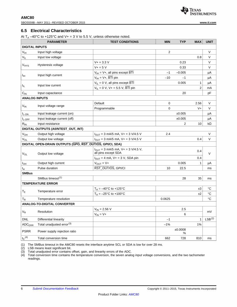
6.5 Electrical CharacteristicsAt TA –40°C to +125°C and V+ = 3 V to 5.5 V, unless otherwise noted.
PARAMETER TEST CONDITIONS MIN TYP MAX UNITDIGITAL INPUTSVIH Input high voltage 2 VVIL Input low voltage 0.8 V
V+ = 3.3 V 0.23 VVHYS Hysteresis voltage
V+ = 5 V 0.33 VVIH = V+, all pins except BTI –1 –0.005 µA
IIH Input high currentVIH = V+, BTI pin –10 –1 µAVIL = 0 V, all pins except BTI 0.005 1 µA
IIL Input low currentVIL = 0 V, V+ = 5.5 V, BTI pin 2 mA
CIN Input capacitance 20 pFANALOG INPUTS
Default 0 2.56 VVIN Input voltage range
Programmable 0 V+ VIL-ON Input leakage current (on) ±0.005 µAIL-OFF Input leakage current (off) ±0.005 µARIN Input resistance 2 10 kΩDIGITAL OUTPUTS (A0/NTEST_OUT, INT)VOH Output high voltage IOUT = 3 mA/5 mA, V+ = 3 V/4.5 V 2.4 VVOL Output low voltage IOUT = 3 mA/5 mA, V+ = 3 V/4.5 V 0.4 VDIGITAL OPEN-DRAIN OUTPUTS (GPO, RST_OUT/OS, GPI/CI, SDA)
IOUT = 3 mA/5 mA, V+ = 3 V/4.5 V, 0.4all pins except SDAVOL Output low voltage VIOUT = 4 mA, V+ = 3 V, SDA pin 0.4
IOH Output high current VOUT = V+ 0.005 1 µAtw Pulse duration RST_OUT/OS, GPI/CI 10 22.5 msSMBus
SMBus timeout (1) 28 35 msTEMPERATURE ERROR
TA = –40°C to +125°C ±3 °CTE Temperature error
TA = –25°C to +100°C ±2 °CTR Temperature resolution 0.0625 °CANALOG-TO-DIGITAL CONVERTER
VIN = 2.56 V 2.5VR Resolution mV
VIN = V+ 6DNL Differential linearity –1 1 LSB (2)
ADCERR Total unadjusted error (3) –1% 1%±0.0008PSRR Power supply rejection ratio %
tC(4) Total conversion time 662 728 810 ms
(1) The SMBus timeout in the AMC80 resets the interface anytime SCL or SDA is low for over 28 ms.(2) LSB means least significant bit.(3) Total unadjusted error contains offset, gain, and linearity errors of the ADC.(4) Total conversion time contains the temperature conversion, the seven analog input voltage conversions, and the two tachometer
readings.
6 Submit Documentation Feedback Copyright © 2011–2015, Texas Instruments Incorporated
Product Folder Links: AMC80
AMC80www.ti.com SBOS559B –MAY 2011–REVISED OCTOBER 2015
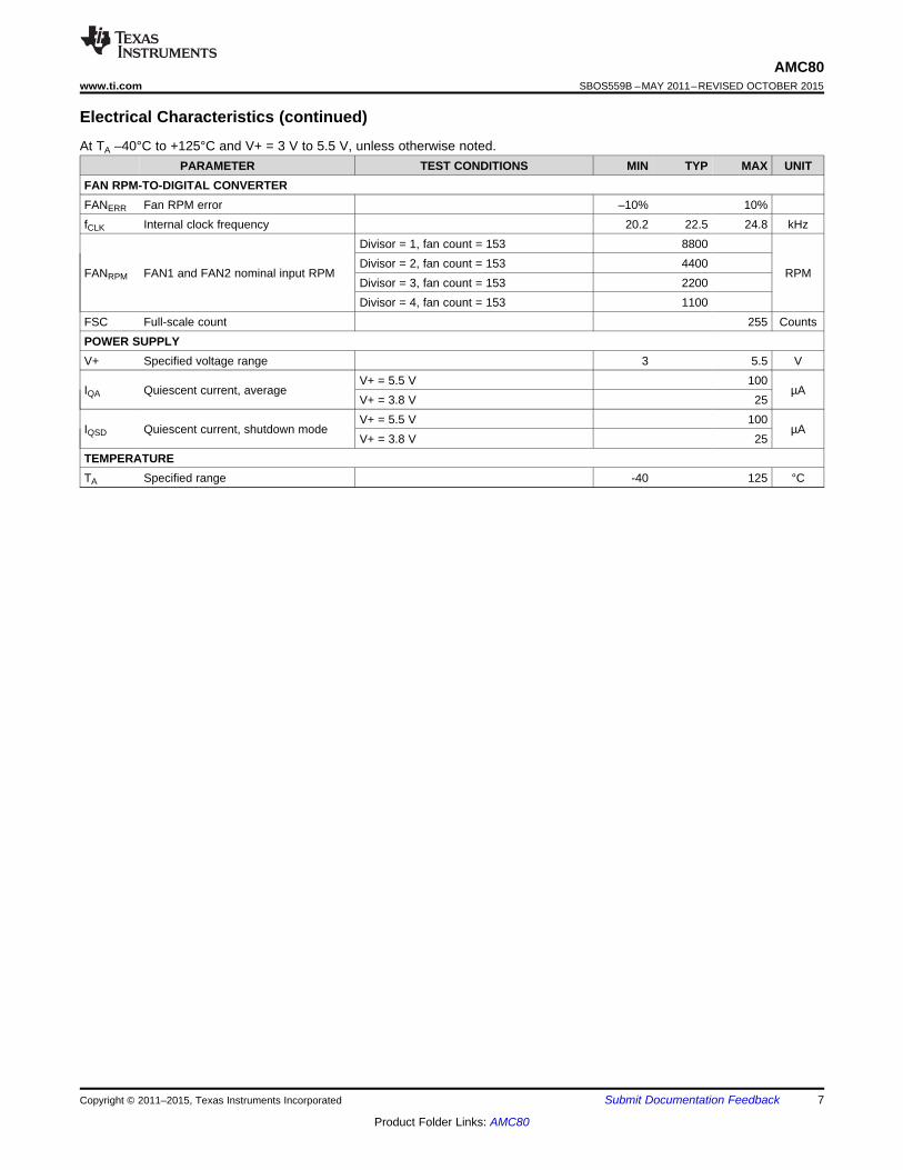
Electrical Characteristics (continued)At TA –40°C to +125°C and V+ = 3 V to 5.5 V, unless otherwise noted.
PARAMETER TEST CONDITIONS MIN TYP MAX UNITFAN RPM-TO-DIGITAL CONVERTERFANERR Fan RPM error –10% 10%fCLK Internal clock frequency 20.2 22.5 24.8 kHz
Divisor = 1, fan count = 153 8800Divisor = 2, fan count = 153 4400
FANRPM FAN1 and FAN2 nominal input RPM RPMDivisor = 3, fan count = 153 2200Divisor = 4, fan count = 153 1100
FSC Full-scale count 255 CountsPOWER SUPPLYV+ Specified voltage range 3 5.5 V
V+ = 5.5 V 100IQA Quiescent current, average µA
V+ = 3.8 V 25V+ = 5.5 V 100
IQSD Quiescent current, shutdown mode µAV+ = 3.8 V 25
TEMPERATURETA Specified range -40 125 °C
Copyright © 2011–2015, Texas Instruments Incorporated Submit Documentation Feedback 7
Product Folder Links: AMC80

SCL
SDA
t(LOW)tR tF t(HDSTA)
t(HDSTA)
t(HDDAT)
t(BUF)
t(SUDAT)
t(HIGH) t(SUSTA)t(SUSTO)
P S S P
AMC80SBOS559B –MAY 2011–REVISED OCTOBER 2015 www.ti.com
6.6 Timing RequirementsAt TA –40°C to +125°C and VS = 3V to 5.5V, unless otherwise noted.
FAST MODE (1) HIGH-SPEED MODE (1)
MIN MAX MIN MAX UNITf(SCL) SCL operating frequency 10 400 10 3400 kHzt(BUF) Bus free time between STOP and START conditions 600 160 ns
Hold time after repeated START condition. After thist(HDSTA) 600 160 nsperiod, the first clock is generated.t(SUSTA) Repeated START condition setup time 600 160 nst(SUSTO) STOP condition setup time 600 160 nst(HDDAT) Data hold time 0 (2) 0 (3) nst(SUDAT) Data setup time 100 10 nst(LOW) Clock low period 1300 160 nst(HIGH) Clock high period 600 60 nstR Clock/Data input rise time 300 160 nstF Clock/Data input fall time 300 160 ns
(1) Values based on a statistical analysis of a one-time sample of devices. Minimum and maximum values are not specified and notproduction tested.
(2) For cases when the fall time of SCL is less than 20 ns and/or the rise time or fall time of SDA is less than 20 ns, the hold time should begreater than 20 ns.
(3) For cases when the fall time of SCL is less than 10 ns and/or the rise or fall time of SDA is less than 10 ns, the hold time should begreater than 10 ns.
Figure 1. Serial Bus Interface Timing
8 Submit Documentation Feedback Copyright © 2011–2015, Texas Instruments Incorporated
Product Folder Links: AMC80

0.16
0.12
0.08
0.04
5.554.543.532.5
Tem
pe
ratu
re E
rro
r (
C)
°
V+ (V)
240
220
200
180
160
140
120
100
5.554.543.532.5
I(
A)
mQ
T
V+ (V)
45
40
35
30
25
20
15
10
5
0
5.554.543.532.5
I(
A)
mQ
SD
V+ (V)
50
45
40
35
30
25
20
15
10
5
0
5.554.543.532.5
I(
A)
mQ
A
V+ (V)
220
200
180
160
140
120
100
5.554.543.532.5
I(
A)
mQ
V
V+ (V)
AMC80www.ti.com SBOS559B –MAY 2011–REVISED OCTOBER 2015
6.7 Typical CharacteristicsAt TA = +25°C and V+ = 3 V to 5.5 V, unless otherwise noted.
Figure 2. Average Quiescent Current vs Supply Voltage Figure 3. Quiescent Current During Voltage Conversion vsSupply Voltage
Figure 4. Quiescent Current During Temperature Figure 5. Quiescent Current During Shutdown vs SupplyConversion vs Supply Voltage Voltage
Figure 6. Temperature Error vs Supply Voltage
Copyright © 2011–2015, Texas Instruments Incorporated Submit Documentation Feedback 9
Product Folder Links: AMC80

TemperatureSensor
IN0Addr = 20h
InterruptMasking
andInterruptControl
Interface and Control
AMC80
CH0
CH6
AnalogInputs
GPI(CI)
INT_IN
BTI
A0/TEST_OUT
SDA
SCL
A1
A2
CH1
CH2
CH3
CH4
CH5
INT
RST_OUT OS/
InterruptOutputs
SerialBus
Interface
10-BitDelta-Sigma
ADC
Fan SpeedCounter
FAN1
FAN2
NTEST_IN RESET_IN/
DigitalInputsandOutputs
InterruptStatus
Registers
Value RAM
IN1Addr = 21h
IN2Addr = 22h
IN3Addr = 23h
IN4Addr = 24h
IN5Addr = 25h
IN6Addr = 26h
TemperatureAddr = 27h
Fan1Addr = 28h
Fan2Addr = 29h
Upper LimitLower Limit
Watchdog
Upper LimitLower LimitUpper LimitLower LimitUpper LimitLower LimitUpper LimitLower LimitUpper LimitLower LimitUpper LimitLower Limit
OSHysteresis
Upper Limit
Upper Limit
HotHysteresis
FanTachometer
Pulse Inputs
GPO
AMC80SBOS559B –MAY 2011–REVISED OCTOBER 2015 www.ti.com
7 Detailed Description
7.1 OverviewThe AMC80 provides seven analog inputs, a temperature sensor, a delta-sigma analog-to-digital converter(ADC), and a variety of inputs and outputs on a single chip. A two-wire SMBus interface is also provided. TheAMC80 can continuously perform power-supply, temperature, and fan monitoring for a variety of applications.The AMC80 is fully pin- and software-compatible with the LM96080 and LM80.
7.2 Functional Block Diagram
7.3 Feature Description
7.3.1 Block Level DescriptionThe AMC80 continuously converts analog inputs to 10-bit resolution using a 2.5-mV least significant bit (LSB)with a default input range of 0 V to 2.56 V, or a 6-mV LSB with a programmable input range of 0 V to V+. Theanalog inputs (CH0 to CH6) are intended for connection to the several power supplies present in any typicalsystem. Temperature can be converted to a 9-bit or 12-bit resolution with either 0.5°C or 0.0625°C LSB,respectively. The FAN1 and FAN2 inputs can be programmed to accept either a fan failure indicator ortachometer signals. Fan failure signals can be programmed to be either active high or active low. Fan inputsmeasure the period of tachometer pulses from the the fans, providing a higher count for lower fan speeds. Thefan inputs are digital inputs with transition levels according to the Digital Inputs section of the ElectricalCharacteristics table. Full-scale fan counts are 255 (8-bit counter), which represent a stopped or very slow fan.Nominal speeds, based on a count of 153, are programmable from 1100 RPM to 8800 RPM. Signal conditioningcircuitry is included to accommodate slow rise and fall times.
The AMC80 provides a number of internal registers:• Configuration Register: Provides control and configuration.• Interrupt Status Registers: Two registers that provide the status of each interrupt alarm.• Interrupt Mask Registers: Allows masking of individual interrupt sources, as well as separate masking for
10 Submit Documentation Feedback Copyright © 2011–2015, Texas Instruments Incorporated
Product Folder Links: AMC80

AMC80www.ti.com SBOS559B –MAY 2011–REVISED OCTOBER 2015
Feature Description (continued)both hardware interrupt outputs.
• Fan Divisor/RST_OUT/OS Register: Bits 0 to 5 of this register contain the divisor bits for the FAN1 andFAN2 inputs. Bits 6 and 7 control the function of the RST_OUT/OS output.
• OS Configuration/Temperature Resolution Register: The configuration of the overtemperature shutdown(OS) is controlled by the lower three bits of this register. Bit 3 enables 12-bit temperature conversions. In 12-bit mode, bits 4 to 7 represent the four LSBs of the temperature measurement. In 9-bit mode, bit 4 representsthe LSB of the temperature measurement.
• Conversion Rate Register: Sets the time interval of the continuous monitoring cycle to either fixed orprogrammable (see the Conversion Rate Count Register for setting the programmable time interval).
• Voltage/Temperature Channel Disable Register: Allows voltage inputs and the local temperatureconversion to be disabled.
• Input Mode Register: Allows voltage inputs to be configured as single-ended or as a differential pair withnormal or reverse polarity.
• ADC Control Register: Bits 0 to 2 set the programmable conversion rate for the 10-bit ADC. Bits 3 to 5 allowfor programmable input full-scale voltage.
• Conversion Rate Count Register: Selects the adjustable time interval when the conversion rate of thecontinuous monitoring cycle is set to programmable.
• Value RAM: The monitoring results (for temperature, voltages, fan counts, and Fan Divisor/RST_OUT/OSRegister limits) are all contained in the Value RAM. The Value RAM consists of 32 bytes. The first 10 bytesare all of the results, the next 20 bytes are the interrupt alarm limits, and the last two bytes are at the upperlocations for manufacturer ID and die revision ID.
The AMC80 SMBus is compatible with both fast mode (400 kHz) and high-speed mode (3.4 MHz) two-wireinterface modes of operation. The AMC80 supports a timeout reset function on SDA and SCL that prevents two-wire bus lockup, and includes an analog filter on the two-wire digital control lines that improves noise immunity.Three address pins (A0 to A2), allow up to eight devices on a single bus. When enabled, the AMC80 starts bycycling through each measurement in sequence, and continuously loops through the sequence based on theConversion Rate Register (address 07h) setting. Each measured value is compared to values stored in the ValueRAM Registers (addresses 2Ah to 3Dh). When the measured value exceeds the programmed limit, the AMC80sets a corresponding interrupt in the Interrupt Status Registers (addresses 01h and 02h). Two output interruptlines (INT and RST_OUT/OS) are available. INT is fully programmable with the ability to mask each interruptsource and each output. The Fan Divisor/RST_OUT/OS Register (address 05h) has control bits that enable ordisable the hardware interrupts. Additional digital inputs are provided for daisy-chaining the interrupt output pin,INT. This configuration is achieved by connecting multiple external temperature sensors (for example, theTMP75) to the board temperature interrupt (BTI) input and/or the GPI/CI input. The chassis intrusion (CI) input isdesigned to accept an active high signal from an external circuit that latches (for example, when the chassis froma server rack is removed).
Copyright © 2011–2015, Texas Instruments Incorporated Submit Documentation Feedback 11
Product Folder Links: AMC80
AMC80SBOS559B –MAY 2011–REVISED OCTOBER 2015 www.ti.com
Feature Description (continued)7.3.2 Temperature MeasurementThe AMC80 ΔVBE-type temperature sensor, is a ΔΣ ADC that performs 9-bit or 12-bit twos complementtemperature conversions. An 8-bit comparator that compares the readings to the user-programmable hot andovertemperature setpoints, and hysteresis values is also incorporated into the AMC80.
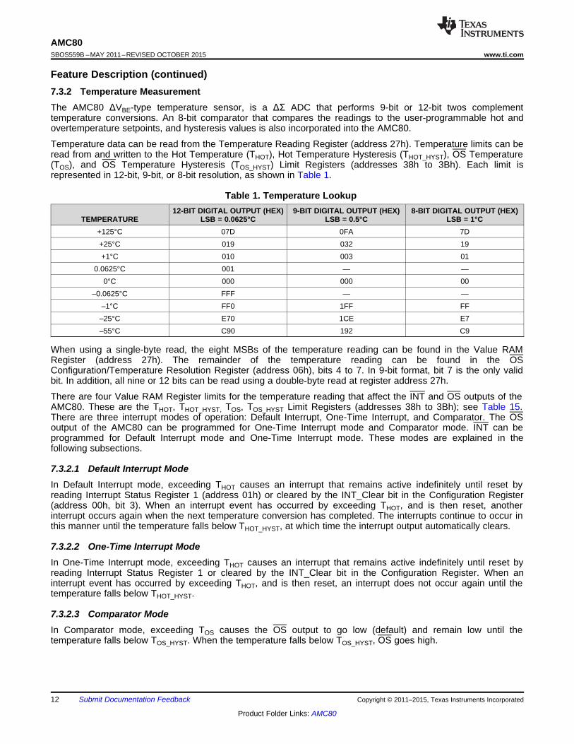
Temperature data can be read from the Temperature Reading Register (address 27h). Temperature limits can beread from and written to the Hot Temperature (THOT), Hot Temperature Hysteresis (THOT_HYST), OS Temperature(TOS), and OS Temperature Hysteresis (TOS_HYST) Limit Registers (addresses 38h to 3Bh). Each limit isrepresented in 12-bit, 9-bit, or 8-bit resolution, as shown in Table 1.
Table 1. Temperature Lookup12-BIT DIGITAL OUTPUT (HEX) 9-BIT DIGITAL OUTPUT (HEX) 8-BIT DIGITAL OUTPUT (HEX)
TEMPERATURE LSB = 0.0625°C LSB = 0.5°C LSB = 1°C+125°C 07D 0FA 7D+25°C 019 032 19+1°C 010 003 01
0.0625°C 001 — —0°C 000 000 00
–0.0625°C FFF — —–1°C FF0 1FF FF–25°C E70 1CE E7–55°C C90 192 C9
When using a single-byte read, the eight MSBs of the temperature reading can be found in the Value RAMRegister (address 27h). The remainder of the temperature reading can be found in the OSConfiguration/Temperature Resolution Register (address 06h), bits 4 to 7. In 9-bit format, bit 7 is the only validbit. In addition, all nine or 12 bits can be read using a double-byte read at register address 27h.
There are four Value RAM Register limits for the temperature reading that affect the INT and OS outputs of theAMC80. These are the THOT, THOT_HYST, TOS, TOS_HYST Limit Registers (addresses 38h to 3Bh); see Table 15.There are three interrupt modes of operation: Default Interrupt, One-Time Interrupt, and Comparator. The OSoutput of the AMC80 can be programmed for One-Time Interrupt mode and Comparator mode. INT can beprogrammed for Default Interrupt mode and One-Time Interrupt mode. These modes are explained in thefollowing subsections.
7.3.2.1 Default Interrupt ModeIn Default Interrupt mode, exceeding THOT causes an interrupt that remains active indefinitely until reset byreading Interrupt Status Register 1 (address 01h) or cleared by the INT_Clear bit in the Configuration Register(address 00h, bit 3). When an interrupt event has occurred by exceeding THOT, and is then reset, anotherinterrupt occurs again when the next temperature conversion has completed. The interrupts continue to occur inthis manner until the temperature falls below THOT_HYST, at which time the interrupt output automatically clears.
7.3.2.2 One-Time Interrupt ModeIn One-Time Interrupt mode, exceeding THOT causes an interrupt that remains active indefinitely until reset byreading Interrupt Status Register 1 or cleared by the INT_Clear bit in the Configuration Register. When aninterrupt event has occurred by exceeding THOT, and is then reset, an interrupt does not occur again until thetemperature falls below THOT_HYST.
7.3.2.3 Comparator ModeIn Comparator mode, exceeding TOS causes the OS output to go low (default) and remain low until thetemperature falls below TOS_HYST. When the temperature falls below TOS_HYST, OS goes high.
12 Submit Documentation Feedback Copyright © 2011–2015, Texas Instruments Incorporated
Product Folder Links: AMC80

Input,Temperature,
and FanWatchdogs
InterruptStatus
Registers
BTI
GPI/CI
INT_IN
InterruptMasking
andControl
RST_OUT OS/
OS Status: R06h, B0
INT
OS Pin Enable: R05h, B6
RST Enable: R05h, B7
RESET: R00h, B4
Temp Watchdog
OS Polarity: R06h, B1
INT Enable: R00h, B1
INT Clear: R00h, B3
INT Polarity Select: R00h, B2
AMC80www.ti.com SBOS559B –MAY 2011–REVISED OCTOBER 2015
7.3.3 Interrupt StructureFigure 7 depicts the interrupt structure of the AMC80.
Figure 7. Interrupt Structure
External interrupt inputs can come from the following sources:• Board Temperature Interrupt (BTI) - This pin is an active low interrupt recommended to come from the
overtemperature shutdown (OS) output of TMP75 temperature sensors. The TMP75 OS output activateswhen its temperature exceeds a programmed threshold. If the temperature of any TMP75 exceeds itsprogrammed limit, BTI is driven low. This action generates an interrupt through bit 1 of Interrupt StatusRegister 2 (address 02h) that notifies the host of a possible overtemperature condition. To disable thisfeature, set bit 1 of Interrupt Mask Register 2 (address 04h) to high. This pin also provides an internal, 10-kΩpull-up resistor.
• GPI/CI - This pin is an active high interrupt from any type of device that detects and captures chassisintrusion violations. This action could be accomplished mechanically, optically, or electrically; circuitry externalto the AMC80 is expected to latch the event. Read this interrupt using bit 4 of Interrupt Status Register 2(address 02h), and disable it using bit 4 of Interrupt Mask Register 2 (address 04h). The design of the AMC80allows this input to go high even with no power applied, and no clamping or other interference with the lineoccurs. This line can also be pulled low by the AMC80 for at least 10ms to reset a typical chassis-intrusioncircuit. Accomplish this reset by setting bit 5 of the Configuration Register (address 00h) to high; this bit isself-clearing.
• INT_IN - This pin is an active low interrupt that provides a way to connect an INT from other devices throughthe AMC80 to the processor. If this pin is pulled low, then bit 7 of Interrupt Status Register 1 (address 01h)goes high, indicating this interrupt detection. Setting bit 1 of the Configuration Register (address 00h) alsoallows the INT pin to go low when INT_IN goes low. To disable this feature, set bit 7 of Interrupt MaskRegister 1 (address 03h) to high.
Device interrupt outputs can come from the following sources:• INT - This pin becomes active whenever INT_IN, BTI, or GPI/CI interrupts. INT is enabled when bit 1 of the
Configuration Register (address 00h) is set high. Bits 2 and 3 of the Configuration Register are also used toset the polarity and state of the INT interrupt line.
• OS - In the Fan Divisor/RST_OUT/OS Register (address 05h), bit 6 (OS Pin Enable), must be set high and bit7 (RST Enable) must be set to low in order to enable the OS function on the RST_OUT/OS pin. The OS pinhas two modes of operation: One-Time Interrupt and Comparator. One-Time Interrupt mode is selected bytaking bit 2 of the OS Configuration/Temperature Resolution Register (address 06h) high. If bit 2 is taken low,then Comparator mode is selected. Unlike the OS pin, the OS bit in Interrupt Status Register 2 (address 02h,bit 5) functions in Default Interrupt and One-Time Interrupt modes. The OS bit can be masked to the INT pinby taking bit 5 in Interrupt Mask Register 2 (address 04h) low.
Reading the Interrupt Status Registers (addresses 01h to 02h) outputs the contents and then resets the registersand the INT pin. The INT pin is also cleared by the INT_Clear bit (address 00h, bit 3) without affecting thecontents of the Interrupt Status Registers. When this bit is high, the AMC80 monitoring loop is inactive;monitoring resumes when this bit is low.
Copyright © 2011–2015, Texas Instruments Incorporated Submit Documentation Feedback 13
Product Folder Links: AMC80

AMC80SBOS559B –MAY 2011–REVISED OCTOBER 2015 www.ti.com
7.4 Programming
7.4.1 Interface and ControlThe SMBus control lines in the AMC80 include SDA, SCL, and the A0 to A2 address pins, which allow up toeight AMC80 devices to be on the same bus. The AMC80 can only operate as a slave device. The SCL linecontrols only the serial interface; all other clock-related functions within the AMC80 (such as the ADC and fancounters) operate with a separate asynchronous internal clock. The default power-on SMBus address for theAMC80 is '0101'(A2)(A1)(A0) binary, where (A2)(A1)(A0) is the SMBus address.
When using the SMBus interface, a write command always consists of the AMC80 SMBus interface addressbyte, followed by the internal address register byte, and then the data byte (see Figure 8).
See Figure 9 for the read operation timing. There are two cases for a read operation:1. If the contents of the Internal Address Register are known, simply read the AMC80 with the SMBus interface
address byte, followed by the data byte read from the ADC80.2. If the internal Address Register contents are unknown, write to the AMC80 with the SMBus interface address
byte, followed by the internal address register bye. Then restart the serial communication with a read thatconsist of the SMBus interface address byte, followed by the data byte read from the AMC80.
Table 2. Register OverviewINTERNAL POWER-ONADDRESS VALUE
REGISTER (HEX) (HEX) NOTESConfiguration Register 00 08Interrupt Status Register 1 01 xx IndeterminateInterrupt Status Register 2 02 xx IndeterminateInterrupt Mask Register 1 03 00Interrupt Mask Register 2 04 00Fan Divisor/RST_OUT/OS Register 05 14 FAN1 and FAN2 divisor = 2 (count of 153 = 4400 RPM)OS Configuration/Temperature Resolution 06 x1 Four MSBs are indeterminateRegisterConversion Rate Register 07 40Voltage/Temperature Channel Disable 08 00 Allows voltage monitoring inputs to be disabledRegisterInput Mode Register 09 00ADC Control Register 0A 02Conversion Rate Count Register 0B 40Value RAM Register 20 to 29 xx IndeterminateValue RAM Register 2A to 3D xx IndeterminateValue RAM Register 3E 80Value RAM Register 3F 09
14 Submit Documentation Feedback Copyright © 2011–2015, Texas Instruments Incorporated
Product Folder Links: AMC80

Frame 1 Two-Wire Slave Address Byte Frame 2 Pointer Register Byte
0
Start By
Master
ACK By
AMC80
ACK By
AMC80
Frame 3 Two-Wire Slave Address Byte Frame 4 Data Byte 1 Read Register
Start By
Master
ACK By
AMC80
ACK By
Master(2)
From
AMC80
1 9 1 9
1 9 1 9
SDA
SCL
1 0 1 R/W P7 P6 P5 P4 P3 P2 P1 P0
¼
¼
¼
SDA
(Continued)
SCL
(Continued)
SDA
(Continued)
SCL
(Continued)
0 1 0 1
A2(1)
A1(1)
A0(1)
A2(1)
A1(1)
A0(1) R/W D7 D6 D5 D4 D3 D2 D1 D0
Frame 5 Data Byte 2 Read Register
Stop By
Master
ACK By
Master(3)
From
AMC80
1 9
D7 D6 D5 D4 D3 D2 D1 D0
Stop By
Master
Frame 1 Two-Wire Slave Address Byte Frame 2 Pointer Register Byte
Frame 4 Data Byte 2
0
Start By
Master
ACK By
AMC80
ACK By
AMC80
ACK By
AMC80
Stop By
Master
1 9 1
1
D7 D6 D5 D4 D3 D2 D1 D0
9
Frame 3 Data Byte 1
ACK By
AMC80
1
D7SDA
(Continued)
SCL
(Continued)
D6 D5 D4 D3 D2 D1 D0
9
9
SDA
SCL
1 0 1 A2(1) A1(1) A0(1) R/W P7 P6 P5 P4 P3 P2 P1 P0 ¼
¼
AMC80www.ti.com SBOS559B –MAY 2011–REVISED OCTOBER 2015
(1) The values of A0, A1, and A2 are determined by the A0, A1, and A2 pins, respectively.
Figure 8. Two-Wire Timing for Write Word Format
(1) The values of A0, A1, and A2 are determined by the A0, A1, and A2 pins, respectively.(2) Master should leave SDA high to terminate a single-byte read operation.(3) Master should leave SDA high to terminate a two-byte read operation.
Figure 9. Two-Wire Timing for Read Word Format
Copyright © 2011–2015, Texas Instruments Incorporated Submit Documentation Feedback 15
Product Folder Links: AMC80

AMC80SBOS559B –MAY 2011–REVISED OCTOBER 2015 www.ti.com
7.5 Register Map
7.5.1 Configuration Register
Table 3. Configuration Register (Address = 00h, Default = 08h)BIT NAME TYPE DESCRIPTION0 Start R/W '1' enables startup of monitoring activity; '0' puts device in shutdown mode.1 INT Enable R/W '1' enables the INT output.2 INT Polarity Select R/W '1' selects active-high, open-source output; '0' selects active-low, open-drain output.
'1' disables the INT output without affecting the contents of the Interrupt Status Registers.3 INT_Clear R/W The device stops monitoring and resumes on a '0'.'1' outputs an active-low reset signal at RST_OUT, if bit 7 and bit 6 in the Fan Divisor/
4 RESET R/W Register (address 05h) are set to '1' and '0', respectively. This bit is cleared when the pulsebecomes inactive.
5 Chassis Clear R/W '1' clears the GPI/CI pin. This bit clears itself after 10ms.6 GPO R/W '1' drives the GPO pin low.7 INITIALIZATION R/W '1' restores power-on-default values to the registers. This bit is self-clearing
7.5.2 Interrupt Status Registers
Table 4. Interrupt Status Register 1 (Address = 01h, Default = xxh; see Table 2)BIT NAME TYPE DESCRIPTION0 CH0 Read '1' indicates a high or low limit has been exceeded.1 CH1 Read '1' indicates a high or low limit has been exceeded.2 CH2 Read '1' indicates a high or low limit has been exceeded.3 CH3 Read '1' indicates a high or low limit has been exceeded.4 CH4 Read '1' indicates a high or low limit has been exceeded.5 CH5 Read '1' indicates a high or low limit has been exceeded.6 CH6 Read '1' indicates a high or low limit has been exceeded.7 INT_IN Read '1' indicates that a low signal has been detected on the INT_IN pin.
Table 5. Interrupt Status Register 2 (Address = 02h, Default = xxh; see Table 2)BIT NAME TYPE DESCRIPTION
'1' indicates a high or low limit has been exceeded. One-Time Interrupt and Default Interrupt0 Hot Temperature Read modes are supported and can be set by bit 6 of Interrupt Mask Register 2 (address 04h).1 BTI Read '1' indicates that an interrupt has occurred from the BTI input pin.2 FAN 1 Read '1' indicates that a fan count limit has been exceeded.3 FAN 2 Read '1' indicates that a fan count limit has been exceeded.4 GPI/CI Read '1' indidates that GPI/CI has gone high.
'1' indicates a high or low temperature limit has been exceeded. One-Time Interrupt and5 OS Read Default Interrupt modes are supported and can be set by bit 7 of Interrupt Mask Register 2
(address 04h).6 Reserved Read This bit is reserved.7 Reserved Read This bit is reserved.
16 Submit Documentation Feedback Copyright © 2011–2015, Texas Instruments Incorporated
Product Folder Links: AMC80

AMC80www.ti.com SBOS559B –MAY 2011–REVISED OCTOBER 2015
7.5.3 Interrupt Mask Registers
Table 6. Interrupt Mask Register 1 (Address = 03h, Default = 00h)BIT NAME TYPE DESCRIPTION0 CH0 R/W1 CH1 R/W2 CH2 R/W3 CH3 R/W
'1' disables the corresponding interrupt status bit in Table 4 to trigger the INT interrupt.4 CH4 R/W5 CH5 R/W6 CH6 R/W7 INT_IN R/W
Table 7. Interrupt Mask Register 2 (Address = 04h, Default = 00h)BIT NAME TYPE DESCRIPTION0 Hot Temperature R/W1 BTI R/W2 FAN 1 R/W
'1' disables the corresponding interrupt status bit in Table 5 to trigger the INT interrupt.3 FAN 2 R/W4 GPI/CI R/W5 OS R/W
INT Interrupt Mode6 R/W '0' selects Default Interrupt mode. '1' selects One-Time Interrupt mode.SelectOS Interrupt Mode7 R/W '0' selects Comparator mode. '1' selects One-Time Interrupt mode.Select
7.5.4 Fan Divisor/RST_OUT/OS Register
Table 8. Fan Divisor/RST_OUT/OS Register (Address = 05h, Default = 14h)BIT NAME TYPE DESCRIPTION0 FAN1 Mode Select R/W '1' selects the level-sensitive input mode. '0' selects the fan count mode for the FAN1 input.1 FAN2 Mode Select R/W '1' selects the level-sensitive input mode. '0' selects the fan count mode for the FAN2 input.2 FAN1 RPM Control 1 R/W FAN1 speed control:
'00' = divide by 1.'01' = divide by 2.'10' = divide by 4.
3 FAN1 RPM Control 0 R/W '11' = divide by 8.If level-sensitive input is selected, '01' selects an active-low input and '00' selects an active-high input.
4 FAN2 RPM Control 1 R/W FAN2 speed control:'00' = divide by 1.'01' = divide by 2.'10' = divide by 4.
5 FAN2 RPM Control 0 R/W '11' = divide by 8.If level select input is selected, '01' selects an active-low input and '00' selects an active-highinput.'1' enables OS mode on the RST_OUT/OS pin when bit 7 is set to '0'.6 OS Pin Enable R/W NOTE: When bits 6 and 7 are both set to '1', the RST_OUT/OS pin is disabled.'1' enables RST_OUT mode on the RST_OUT/OS pin when bit 6 is set to '0'.7 RST_OUT Pin Enable R/W NOTE: When bits 6 and 7 are both set to '1', the RST_OUT/OS pin is disabled.
Copyright © 2011–2015, Texas Instruments Incorporated Submit Documentation Feedback 17
Product Folder Links: AMC80

AMC80SBOS559B –MAY 2011–REVISED OCTOBER 2015 www.ti.com
7.5.5 OS Configuration/Temperature Resolution Register
Table 9. OS Configuration/Temperature Resolution Register (Address = 06h, Default = x1h; see Table 2)BIT NAME TYPE DESCRIPTION0 OS Status Read This bit mirrors the state of the RST_OUT/OS pin when in OS mode.1 OS Polarity R/W '1' selects OS to be active-high '0' selects OS to be active-low.2 OS Mode Select R/W '1' selects One-Time-Interrupt mode; '0' selects Comparator mode.
Temperature '1' selects 11-bit plus sign resolution temperature conversion; '0' selects the default 8-bit plus3 R/WResolution Control sign resolution temperature conversion.4 Temp3 R/W5 Temp2 R/W The lower four LSBs of the 11-bit plus sign temperature data. For 8-bit plus sign temperature
data, bit 7 is the LSB and bits 4 to 6 are undefined.6 Temp1 R/W7 Temp0 R/W
7.5.6 Conversion Rate Register
Table 10. Conversion Rate Register (Address = 07h, Default = 40h)BIT NAME TYPE DESCRIPTION
Controls conversion rate:'0' = Programmable conversion rate by the following formula:Monitoring delay = (ms) = 1.42 × (8 × N + 6)0 CR1 R/Wwhere N can be set by bits 7:0 in the Conversion Rate Count Register (address 0Bh).'1' = Continuous conversion.
1 Reserved R/W '0' must be written to this bit.2 Reserved R/W '0' must be written to this bit.3 Reserved R/W '0' must be written to this bit.4 Reserved R/W '0' must be written to this bit.5 Reserved R/W '0' must be written to this bit.6 Reserved R/W '0' must be written to this bit.7 Reserved R/W '0' must be written to this bit.
7.5.7 Voltage/Temperature Channel Disable Register
Table 11. Voltage/Temperature Channel Disable Register (Address = 08h, Default = 00h)BIT NAME TYPE DESCRIPTION0 CH0 R/W '1' disables conversions and suppresses error events; Value RAM Register reads '0' for CH0.1 CH1 R/W '1' disables conversions and suppresses error events; Value RAM Register reads '0' for CH1.2 CH2 R/W '1' disables conversions and suppresses error events; Value RAM Register reads '0' for CH2.3 CH3 R/W '1' disables conversions and suppresses error events; Value RAM Register reads '0' for CH3.4 CH4 R/W '1' disables conversions and suppresses error events; Value RAM Register reads '0' for CH4.5 CH5 R/W '1' disables conversions and suppresses error events; Value RAM Register reads '0' for CH5.6 CH6 R/W '1' disables conversions and suppresses error events; Value RAM Register reads '0' for CH6.
'1' disables conversions and suppresses error events; Value RAM Register reads '0' for7 Temp R/W temperature.
18 Submit Documentation Feedback Copyright © 2011–2015, Texas Instruments Incorporated
Product Folder Links: AMC80

AMC80www.ti.com SBOS559B –MAY 2011–REVISED OCTOBER 2015
7.5.8 Input Mode Register
Table 12. Input Mode Register (Address = 09h, Default = 00h)BIT NAME TYPE DESCRIPTION
When set to '1', CH0 and CH1 operate as a differential input.0 Diff01 R/W When set to '0', CH0 and CH1 operate as 2 single-ended inputs.When bit 0 = '1', CH0 and CH1 differential inputs are setup in normal polarity mode when
1 Pol01 R/W this bit is set to '1', and in reverse polarity mode when this bit is set to '0'.When bit 0 is set to “0”, this bit is ignored.When set to '1', CH2 and CH3 operate as a differential input.2 Diff23 R/W When set to '0', CH2 and CH3 operate as 2 single-ended inputs.When bit 0 = '1', CH2 and CH3 differential inputs are setup in normal polarity mode when
3 Pol23 R/W this bit is set to '1', and in reverse polarity mode when this bit is set to '0'.When bit 0 is set to “0”, this bit is ignored.When set to '1', CH4 and CH5 operate as a differential input.4 Diff45 R/W When set to '0', CH4 and CH5 operate as 2 single-ended inputs.When bit 0 = '1', CH4 and CH5 differential inputs are setup in normal polarity mode when
5 Pol45 R/W this bit is set to '1', and in reverse polarity mode when this bit is set to '0'.When bit 0 is set to “0”, this bit is ignored.
6 Reserved R/W '0' must be written to this bit.7 Reserved R/W '0' must be written to this bit.
7.5.9 ADC Control Register
Table 13. ADC Control Register (Address = 0Ah, Default = 02h)BIT NAME TYPE DESCRIPTION0 DR2 R/W The 10-bit ADC conversion rate for the analog inputs is set as follows:
000 = 0.512 kHz1 DR1 R/W 001 = 1 kHz010 = 1.98 kHz011 = 3.6 kHz100 = 6.3 kHz2 DR0 R/W 101 = 9.8 kHz110 = 13.15 kHz111 = 13.15 kHz
3 PGA2 R/W The full-scale analog input range is set as follows:000 = 2.56 V4 PGA1 R/W 001 = VDD010 = 4.096 V or VDD (whichever is less)011 = 2.048 V100 = 1.024 V5 PGA0 R/W 101 = 0.512 V110 = 0.256 V111 = 0.256 V
6 Reserved R/W '0' must be written to this bit.7 Reserved R/W '0' must be written to this bit.
Copyright © 2011–2015, Texas Instruments Incorporated Submit Documentation Feedback 19
Product Folder Links: AMC80

AMC80SBOS559B –MAY 2011–REVISED OCTOBER 2015 www.ti.com
7.5.10 Conversion Rate Count Register
Table 14. Conversion Rate Count Register (Address = 0Bh, Default = 40h)BIT NAME TYPE DESCRIPTION0 CRC7 R/W1 CRC6 R/W When bit 0 of the Conversion Rate Register (address 07h) is set to '0', the monitoring
conversion delay can be programmed as follows:2 CRC5 R/W0000000 = 0
3 CRC4 R/W 0000001 = 10000010 = 24 CRC3 R/W… … …
5 CRC2 R/W 1111111 = 255When bit 0 of the Conversion Rate Register is set to '1', these bits are ignored.6 CRC1 R/W
7 CRC0 R/W
7.5.11 Value Ram Register
Table 15. Value RAM Register (Addresses = 20h to 3Fh)ADDRESS (HEX) DESCRIPTION
20 CH0 reading (10-bit)21 CH1 reading (10-bit)22 CH2 reading (10-bit)23 CH3 reading (10-bit)24 CH4 reading (10-bit)25 CH5 reading (10-bit)26 CH6 reading (10-bit)27 Temperature reading (9-bit or 12-bit for easy readback)28 FAN1 reading29 FAN2 reading2A CH0 high limit2B CH0 low limit2C CH1 high limit2D CH1 low limit2E CH2 high limit2F CH2 low limit30 CH3 high limit31 CH3 low limit32 CH4 high limit33 CH4 low limit34 CH5 high limit35 CH5 low limit36 CH6 high limit37 CH6 low limit38 Hot temperature high limit (THOT)39 Hot temperature hysteresis low limit (THOT_HYST)3A OS temperature high limit (TOS)3B OS temperature hysteresis low limit (TOS_HYST)3C FAN1 fan count limit3D FAN2 fan count limit3E Manufacturer ID (always defaults to 80h)3F Die revision ID (always defaults to 08h)
20 Submit Documentation Feedback Copyright © 2011–2015, Texas Instruments Incorporated
Product Folder Links: AMC80

AMC80www.ti.com SBOS559B –MAY 2011–REVISED OCTOBER 2015
8 Application and Implementation
NOTEInformation in the following applications sections is not part of the TI componentspecification, and TI does not warrant its accuracy or completeness. TI’s customers areresponsible for determining suitability of components for their purposes. Customers shouldvalidate and test their design implementation to confirm system functionality.
8.1 Application Information
8.1.1 Device Power-OnThe AMC80 undergoes a power-on-reset condition when power is first applied to the device, or when theConfiguration Register INITIALIZATION bit (address 00h, bit 7) is set high; this bit automatically clears afterbeing set. The AMC80 can also be forced to a reset condition by taking the NTEST_IN/RESET_IN pin low for atleast 50 ns.
To start the AMC80 monitoring functions (temperature, analog inputs, and fan speeds), write to the ConfigurationRegister with a '0' to INT_Clear (bit 3) and a '1' to Start (bit 0). The AMC80 then performs continuous monitoringof all temperature, analog inputs, and fan speeds. The sequence of items that are monitored (except for thetemperature reading) corresponds to locations in the Value RAM, respectively:1. Temperature2. CH03. CH14. CH25. CH36. CH47. CH58. CH69. Fan 110. Fan 2
The conversion results are available in the Value RAM (addresses 20h to 29h). Conversions can be read at anytime and provide the result of the last conversion. A typical sequence of events after AMC80 power-on consistsof these actions:1. Set alarm limits2. Set interrupt masks3. Start the AMC80 monitoring process
Copyright © 2011–2015, Texas Instruments Incorporated Submit Documentation Feedback 21
Product Folder Links: AMC80

Count =1.35 10´
´
6
RPM Divisor
AMC80SBOS559B –MAY 2011–REVISED OCTOBER 2015 www.ti.com
Application Information (continued)8.1.2 Analog InputsIn the default state, the 10-bit ADC has a 2.5-mV LSB, yielding a 2.56-V full-scale input range. The input rangecan also be programmed with several values up to the V+ full-scale input range with a 6-mV LSB. These settingsare programmed by bits 3 to 5 in the ADC Control Register.
In most applications, the analog inputs are often connected to power supplies. The voltage inputs should beattenuated with external resistors to any desired value within the input range.
CAUTIONCare should be taken not to exceed V+ on the device input pins at any time.
In select applications where inputs to be monitored are differential in nature, analog inputs (CH0 to CH5) can beconfigured as up to three differential pairs (inputs 0-1, 2-3, and 4-5) by setting bits 0, 2, and 4 in the Input ModeRegister. If needed, the input pair polarity can be changed by setting bits 1, 3, and 5 in the Input Mode Register.
8.1.3 Fan InputsInputs are provided on the AMC80 for signals from fans equipped with tachometer outputs. Signal conditioning inthe AMC80 accommodates the slow rise and fall times typical of fan tachometer outputs. The maximum inputsignal range is 0 V to 5.5 V. In the event that these inputs are supplied from fan outputs that exceed 0 V to 5.5 V,either resistive division or diode clamping must be included to keep inputs within an acceptable range.
The Fan Inputs gate an internal 22.5-kHz oscillator for one period of the Fan signal into an 8-bit counter(maximum count = 255). The default divisor is set to 2 (choices are 1, 2, 4, and 8) providing a nominal count of153 for a 4400 RPM fan with two pulses per revolution. Typical practice is to consider 70% of normal RPM a fanfailure, at which point the count will be 219. The fan count can be determined as shown in Equation 1:
Where:RPM = fan speedDivisor = fan 1 or fan 2 divisor set through the Fan_Divisor/RST_OUT/OS Register (address 05h) (1)
FAN1 and FAN2 inputs can also be programmed to be level-sensitive interrupt inputs. Fans that provide only onepulse per revolution require a divisor that is set twice as high as fans that provide two pulses, thus maintaining anominal fan count of 153. Therefore, using Equation 1, the divisor should be set to 4 for a fan that provides onepulse per revolution with a nominal RPM of 4400.
22 Submit Documentation Feedback Copyright © 2011–2015, Texas Instruments Incorporated
Product Folder Links: AMC80

AMC80www.ti.com SBOS559B –MAY 2011–REVISED OCTOBER 2015
9 Device and Documentation Support
9.1 Community ResourcesThe following links connect to TI community resources. Linked contents are provided "AS IS" by the respectivecontributors. They do not constitute TI specifications and do not necessarily reflect TI's views; see TI's Terms ofUse.
TI E2E™ Online Community TI's Engineer-to-Engineer (E2E) Community. Created to foster collaborationamong engineers. At e2e.ti.com, you can ask questions, share knowledge, explore ideas and helpsolve problems with fellow engineers.
Design Support TI's Design Support Quickly find helpful E2E forums along with design support tools andcontact information for technical support.
9.2 TrademarksE2E is a trademark of Texas Instruments.All other trademarks are the property of their respective owners.
9.3 Electrostatic Discharge CautionThis integrated circuit can be damaged by ESD. Texas Instruments recommends that all integrated circuits be handled withappropriate precautions. Failure to observe proper handling and installation procedures can cause damage.
ESD damage can range from subtle performance degradation to complete device failure. Precision integrated circuits may be moresusceptible to damage because very small parametric changes could cause the device not to meet its published specifications.
9.4 GlossarySLYZ022 — TI Glossary.
This glossary lists and explains terms, acronyms, and definitions.
10 Mechanical, Packaging, and Orderable InformationThe following pages include mechanical, packaging, and orderable information. This information is the mostcurrent data available for the designated devices. This data is subject to change without notice and revision ofthis document. For browser-based versions of this data sheet, refer to the left-hand navigation.
Copyright © 2011–2015, Texas Instruments Incorporated Submit Documentation Feedback 23
Product Folder Links: AMC80

PACKAGE OPTION ADDENDUM
www.ti.com 23-Dec-2015
Addendum-Page 1
PACKAGING INFORMATION
Orderable Device Status(1)
Package Type PackageDrawing
Pins PackageQty
Eco Plan(2)
Lead/Ball Finish(6)
MSL Peak Temp(3)
Op Temp (°C) Device Marking(4/5)
Samples
AMC80AIPW ACTIVE TSSOP PW 24 60 Green (RoHS& no Sb/Br)
CU NIPDAU Level-2-260C-1 YEAR -40 to 125 AMC80A
AMC80AIPWR ACTIVE TSSOP PW 24 2000 Green (RoHS& no Sb/Br)
CU NIPDAU Level-2-260C-1 YEAR -40 to 125 AMC80A
(1) The marketing status values are defined as follows:ACTIVE: Product device recommended for new designs.LIFEBUY: TI has announced that the device will be discontinued, and a lifetime-buy period is in effect.NRND: Not recommended for new designs. Device is in production to support existing customers, but TI does not recommend using this part in a new design.PREVIEW: Device has been announced but is not in production. Samples may or may not be available.OBSOLETE: TI has discontinued the production of the device.
(2) Eco Plan - The planned eco-friendly classification: Pb-Free (RoHS), Pb-Free (RoHS Exempt), or Green (RoHS & no Sb/Br) - please check http://www.ti.com/productcontent for the latest availabilityinformation and additional product content details.TBD: The Pb-Free/Green conversion plan has not been defined.Pb-Free (RoHS): TI's terms "Lead-Free" or "Pb-Free" mean semiconductor products that are compatible with the current RoHS requirements for all 6 substances, including the requirement thatlead not exceed 0.1% by weight in homogeneous materials. Where designed to be soldered at high temperatures, TI Pb-Free products are suitable for use in specified lead-free processes.Pb-Free (RoHS Exempt): This component has a RoHS exemption for either 1) lead-based flip-chip solder bumps used between the die and package, or 2) lead-based die adhesive used betweenthe die and leadframe. The component is otherwise considered Pb-Free (RoHS compatible) as defined above.Green (RoHS & no Sb/Br): TI defines "Green" to mean Pb-Free (RoHS compatible), and free of Bromine (Br) and Antimony (Sb) based flame retardants (Br or Sb do not exceed 0.1% by weightin homogeneous material)
(3) MSL, Peak Temp. - The Moisture Sensitivity Level rating according to the JEDEC industry standard classifications, and peak solder temperature.
(4) There may be additional marking, which relates to the logo, the lot trace code information, or the environmental category on the device.
(5) Multiple Device Markings will be inside parentheses. Only one Device Marking contained in parentheses and separated by a "~" will appear on a device. If a line is indented then it is a continuationof the previous line and the two combined represent the entire Device Marking for that device.
(6) Lead/Ball Finish - Orderable Devices may have multiple material finish options. Finish options are separated by a vertical ruled line. Lead/Ball Finish values may wrap to two lines if the finishvalue exceeds the maximum column width.
Important Information and Disclaimer:The information provided on this page represents TI's knowledge and belief as of the date that it is provided. TI bases its knowledge and belief on informationprovided by third parties, and makes no representation or warranty as to the accuracy of such information. Efforts are underway to better integrate information from third parties. TI has taken andcontinues to take reasonable steps to provide representative and accurate information but may not have conducted destructive testing or chemical analysis on incoming materials and chemicals.TI and TI suppliers consider certain information to be proprietary, and thus CAS numbers and other limited information may not be available for release.
PACKAGE OPTION ADDENDUM
www.ti.com 23-Dec-2015
Addendum-Page 2
In no event shall TI's liability arising out of such information exceed the total purchase price of the TI part(s) at issue in this document sold by TI to Customer on an annual basis.

TAPE AND REEL INFORMATION
*All dimensions are nominal
Device PackageType
PackageDrawing
Pins SPQ ReelDiameter
(mm)
ReelWidth
W1 (mm)
A0(mm)
B0(mm)
K0(mm)
P1(mm)
W(mm)
Pin1Quadrant
AMC80AIPWR TSSOP PW 24 2000 330.0 16.4 6.95 8.3 1.6 8.0 16.0 Q1
PACKAGE MATERIALS INFORMATION
www.ti.com 24-Dec-2015
Pack Materials-Page 1

*All dimensions are nominal
Device Package Type Package Drawing Pins SPQ Length (mm) Width (mm) Height (mm)
AMC80AIPWR TSSOP PW 24 2000 367.0 367.0 38.0
PACKAGE MATERIALS INFORMATION
www.ti.com 24-Dec-2015
Pack Materials-Page 2


IMPORTANT NOTICE
Texas Instruments Incorporated and its subsidiaries (TI) reserve the right to make corrections, enhancements, improvements and otherchanges to its semiconductor products and services per JESD46, latest issue, and to discontinue any product or service per JESD48, latestissue. Buyers should obtain the latest relevant information before placing orders and should verify that such information is current andcomplete. All semiconductor products (also referred to herein as “components”) are sold subject to TI’s terms and conditions of salesupplied at the time of order acknowledgment.TI warrants performance of its components to the specifications applicable at the time of sale, in accordance with the warranty in TI’s termsand conditions of sale of semiconductor products. Testing and other quality control techniques are used to the extent TI deems necessaryto support this warranty. Except where mandated by applicable law, testing of all parameters of each component is not necessarilyperformed.TI assumes no liability for applications assistance or the design of Buyers’ products. Buyers are responsible for their products andapplications using TI components. To minimize the risks associated with Buyers’ products and applications, Buyers should provideadequate design and operating safeguards.TI does not warrant or represent that any license, either express or implied, is granted under any patent right, copyright, mask work right, orother intellectual property right relating to any combination, machine, or process in which TI components or services are used. Informationpublished by TI regarding third-party products or services does not constitute a license to use such products or services or a warranty orendorsement thereof. Use of such information may require a license from a third party under the patents or other intellectual property of thethird party, or a license from TI under the patents or other intellectual property of TI.Reproduction of significant portions of TI information in TI data books or data sheets is permissible only if reproduction is without alterationand is accompanied by all associated warranties, conditions, limitations, and notices. TI is not responsible or liable for such altereddocumentation. Information of third parties may be subject to additional restrictions.Resale of TI components or services with statements different from or beyond the parameters stated by TI for that component or servicevoids all express and any implied warranties for the associated TI component or service and is an unfair and deceptive business practice.TI is not responsible or liable for any such statements.Buyer acknowledges and agrees that it is solely responsible for compliance with all legal, regulatory and safety-related requirementsconcerning its products, and any use of TI components in its applications, notwithstanding any applications-related information or supportthat may be provided by TI. Buyer represents and agrees that it has all the necessary expertise to create and implement safeguards whichanticipate dangerous consequences of failures, monitor failures and their consequences, lessen the likelihood of failures that might causeharm and take appropriate remedial actions. Buyer will fully indemnify TI and its representatives against any damages arising out of the useof any TI components in safety-critical applications.In some cases, TI components may be promoted specifically to facilitate safety-related applications. With such components, TI’s goal is tohelp enable customers to design and create their own end-product solutions that meet applicable functional safety standards andrequirements. Nonetheless, such components are subject to these terms.No TI components are authorized for use in FDA Class III (or similar life-critical medical equipment) unless authorized officers of the partieshave executed a special agreement specifically governing such use.Only those TI components which TI has specifically designated as military grade or “enhanced plastic” are designed and intended for use inmilitary/aerospace applications or environments. Buyer acknowledges and agrees that any military or aerospace use of TI componentswhich have not been so designated is solely at the Buyer's risk, and that Buyer is solely responsible for compliance with all legal andregulatory requirements in connection with such use.TI has specifically designated certain components as meeting ISO/TS16949 requirements, mainly for automotive use. In any case of use ofnon-designated products, TI will not be responsible for any failure to meet ISO/TS16949.
Products ApplicationsAudio www.ti.com/audio Automotive and Transportation www.ti.com/automotiveAmplifiers amplifier.ti.com Communications and Telecom www.ti.com/communicationsData Converters dataconverter.ti.com Computers and Peripherals www.ti.com/computersDLP® Products www.dlp.com Consumer Electronics www.ti.com/consumer-appsDSP dsp.ti.com Energy and Lighting www.ti.com/energyClocks and Timers www.ti.com/clocks Industrial www.ti.com/industrialInterface interface.ti.com Medical www.ti.com/medicalLogic logic.ti.com Security www.ti.com/securityPower Mgmt power.ti.com Space, Avionics and Defense www.ti.com/space-avionics-defenseMicrocontrollers microcontroller.ti.com Video and Imaging www.ti.com/videoRFID www.ti-rfid.comOMAP Applications Processors www.ti.com/omap TI E2E Community e2e.ti.comWireless Connectivity www.ti.com/wirelessconnectivity
Mailing Address: Texas Instruments, Post Office Box 655303, Dallas, Texas 75265Copyright © 2015, Texas Instruments Incorporated