system architecture for high-speed close-proximity low-power rf memory tags and wireless internet...
TRANSCRIPT

System Architecture for High-speed Close-proximity Low-power RF Memory Tags
and Wireless Internet Access
Iiro Jantunen
Department of Applied Physics
University of Eastern Finland
Kuopio, Finland
Joni Jantunena, Harald Kaaja
a, Sergey Boldyrev
b
aNokia Research Center
bNokia Location & Commerce
Helsinki, Finland
{joni.jantunen, harald.kaaja, sergey.boldyrev}@nokia.com
Le Wang, Jyri Hämäläinen Department of Communications and Networking
Aalto University
Espoo, Finland
{le.wang, jyri.hamalainen}@aalto.fi
Abstract — We have developed an open architecture platform
for implementing passive radio-frequency identification
(RFID) tags with a mass memory for close proximity environ-
ment. Purposes for such mass memory tags are, e.g., multime-
dia files embedded in advertisements or logged sensor data on
a low-power sensor node. In the proposed architecture, a mo-
bile phone acts as the reader that can read or write the
memory of these RFID tags. The architecture also enables
creation of a new type of wireless internet access suitable for,
e.g., internet kiosks. The architecture is designed so that devel-
opment path to a full Network on Terminal Architecture (No-
TA) is feasible. The wireless reading speed of the mass memory
tags, demonstrated to be 112 Mbit/s, is in the range that a 3-
minute 640×320-pixel video can be loaded from the tag to the
phone in less than 10 s. Our solution supports Nokia’s Explore
and Share concept.
Keywords — memory architecture; multimedia systems;
RFID; telephone sets; RF memory tags; Internet connection
I. INTRODUCTION
Today’s mobile phones contain music and video players, which make it possible for consumers to enjoy entertainment while on the move. Acquiring new multimedia content by downloading or streaming, however, is hampered by the high cost and slow speed of Internet connections, as well as by the fact that commonly used physical multimedia formats, such as optical disks, cannot be read with a mobile phone. Thus, to make acquiring new content easier, cheaper and less pow-er-consuming, we propose a new technology based on radio frequency (RF) memory tags readable and writable by mo-bile phones [1].
RFID tags are increasingly a part of our life; transport, traceability, and secure access are some of the main uses of this close proximity technology today. Conventional ma-chine-readable wireless tags, e.g., Near Field Communica-tion (NFC) tags, normally have a very small memory in the range of hundreds of bytes or kilobytes. Some RFID stand-ards include an option to have a flexible-use memory, but the capacity is low compared to factory-set fixed-content memory. Tag selection is based on reading the content in a selected tag memory address (e.g., tag or manufacturer ID).
As the memory capacity of these tags is small, the amount of data to be transferred is also small and power consumption of RF communication is, thus, not a critical issue.
Various research groups have developed improvements to the commercially available RFID technologies. To over-come the storage capacity limitation of passive tags, Wu et al. increase effective tag storage sizes with proposed distrib-uted RFID tag storage infrastructure (D-RFID stores) [2]. Tags would be distributed in space and time in this architec-ture. Ahmed et al. focus on RFID system unreliability and improvements in middleware for object tracking and object location with moving readers or tags [3]. As a result of their research, a virtual reader system architecture was introduced. Ying described a verification platform for RFID reader that utilized Ultra High Frequency (UHF) frequency [4]. This platform is applicable for customization with different RFID standards. Pillin et al. have developed a passive far-field RFID tag using the 2.45 GHz Industrial, Scientific and Med-ical (ISM) band, with a data rate of 4 Mbit/s on the range of 5.5 cm [5]. As an example of a proprietary solution, HP’s Memory Spot tag also works on the 2.45 GHz ISM band and has demonstrated 4 MB memory and 10 Mbit/s data rate but only allowing a touch range [6].
The problems of low data reading rate and small memory size provided by contemporary RFID tags become empha-sized if one considers mobile users reading multimedia files from tags embedded on, e.g., paper media. The attention span of a mobile user is about 10 seconds [7]. Within this period, the user could get a single multimedia content file from a memory tag. Considering a movie trailer, the file size for a 2-minute 640×320-pixel 30-fps (3 Mbit/s), encoded with H.264, would be around 50 MB [8]. The required min-imum data transfer rate from the user point-of-view is thus 50 Mbit/s. This exceeds the maximum data rate available by the 13.56 MHz NFC technology, 848 kbit/s, by a factor of 60. Even the maximum data rate for NFC demonstrated on a laboratory set-up, 6.78 Mbit/s [9], is not enough. When users are getting used to NFC, the speed and storage capacity be-comes quite easily a limiting factor. Thus, there is a need for a new high-speed touch-range RFID radio interface.

The aim of our research has been to develop a high-capacity memory tag, which is wirelessly readable with a mobile phone and suitable for consumer markets in ubimedia applications [10][11]. The mobile phone acts as the user interface for reading and writing passive RF memory tags that contain a high-capacity memory (0.1–1 GB). The rea-soning for the proposed technology was justified by modern trends in non-volatile memory technologies, according to which the power consumption, physical size, and price of memory are continuously decreasing. The technology pre-sented in this paper supports Nokia’s Explore and Share concept, a new way of transferring content (e.g., multimedia, maps, and applications) to a mobile phone [12].
Another use case for the technology presented in this pa-per is an Internet Kiosk, i.e., a short-range hotspot providing access to the Internet. Traditionally, an Internet kiosk is nearly always a computer connected to core network via a backhaul link that can be wired or wireless broadband. The-se Internet Kiosks are typically pay-as-you-go (credit card or pre-paid) or funded by advertisements presented within the kiosk screen.
Nowadays, accessing the Internet freely and securely has become critical for business and recreational needs. Personal wireless terminals (such as mobile phones or laptop comput-ers) are, thus, associated with modern Internet hotspots based on wireless local area network (Wi-Fi) technology. These Wi-Fi hotspots are either free or paid by credit card when logging in and are widely deployed. Another kind of wire-less Internet hotspot is femtocell-based [14], providing a local connectivity through cellular technology such as wide-band code division multiple access (WCDMA). Convention-ally, femtocells are designed for use in a home or small busi-ness to improve indoor wireless coverage. As Bluetooth is a competitive wireless solution especially from energy saving point-of-view, it has also been considered as one technology to enable wireless kiosks [15]. Moreover, NFC featured kiosks allow users to be connected and download multimedia content via NFC-enabled mobile phones [16].
All the wireless internet kiosk or hotspot types mentioned above share the demand of internal power within the phone, the power usage of the connection depending on the technol-ogy and status of the hotspot (distance, amount of devices connected etc.). If draining the battery of the phone is not
acceptable (e.g., while travelling), a wired connection to a power outlet is needed.
In this paper, we describe and specify a network architec-ture, which enables mobile phones to read and write passive RF memory tags and use a RF memory tag based Internet connection. The architecture has been developed and demon-strated in the EU's 6
th Framework Programme (FP) “Micro-
Nano integrated platform for transverse Ambient Intelligence applications” (MINAmI) project [17], and thus the architec-ture is referred to as MINAmI Architecture. Important archi-tecture requirements include openness, modularity, scalabil-ity, and energy efficiency. Openness and modularity are needed to support creation of novel applications and services by 3
rd parties. Scalability of data rate is needed to enable
evolution of the technology along with evolution of multi-media services. Energy efficiency is essential to enable pas-sive operation of the tags as well as to save the phone’s bat-tery.
The paper is organized as follows. In Section II, we in-troduce the system architecture, along with a key component of the architecture, RF memory tags. In Section III, we intro-duce a novel dual-band radio subsystem and its hardware and software implementation. In Section IV, we introduce a new type of power-saving short-range wireless internet access for mobile devices and compare its power use to other available wireless internet access technologies. In Section V, we pre-sent the current status of implementation of the architecture, discuss possibilities for future development, and draw some conclusions.
II. MINAMI ARCHITECTURE
The proposed MINAmI architecture makes use of the mobile phone’s capability of running software and providing several radio interfaces (Fig. 1). The architecture is modular, enabling simpler and faster development of new technical extensions (e.g., RF memory tags). Our architecture focuses on utilization of modularity on component level (e.g., where to plug memory tag functionality) and on communication level (e.g., how the available memory tags are utilized). At close proximity domain (range < 1 m), different tags are communicating locally with a mobile phone. In the present work we have concentrated on the RF memory tags. The sensor parts of the architecture (RFID sensor tags and Blue-
Figure 1. MINAmI Architecture [11]

tooth sensor devices) have been studied in an earlier project [18][19].
The main RF memory tag architectural design challenges include target platform performance obstacles, such as avail-able bus operations (read/write) and power requirements, especially when drawing the line for autonomous operations in the described MINAmI architecture. The other challenge is minimizing changes to the existing system communication layering, only to the external memory stack block. The tech-nological choices in the MINAmI system architecture were able to support both existing standard radios for low-rate sensors, and the high-rate high-capacity memory tags.
A. Network-on-Terminal Architecture (NoTA)
NoTA is a modular service-based system architecture for mobile and embedded devices offering services and applica-tions to each other [20]. The concept is being defined in an open initiative. NoTA is also known as an open device dis-tributed architecture, which allows direct connections be-tween different nodes, within subsystem or between subsys-tems, supporting several physical interfaces within the device or between devices [21]. This architecture also supports both messaging and streaming services. The beauty in the archi-tecture resides in modularity and transport independency. Direct connection between subsystems improves the effi-ciency as they do not necessarily require any processor in-volvement, when subsystems have all the needed functionali-ties available for their independent operations. Transport-specific portion is hidden underneath NoTA communication layering.
NoTA communication layering is built around transport-independent parts and it provides interfaces towards transport-specific parts (Fig. 2). Extension architecture with Device Interconnect Protocol (DIP) enables flexible open-source architecture for different hardware platforms. DIP provides logical links between a requesting subsystem and other subsystems or within a subsystem [21]. DIP is a de-
vice-level communication protocol that can be implemented for various physical interfaces ranging from MIPI (Mobile Industry Processor Interface) high speed serial interfaces and Universal Serial Bus (USB) to wireless interfaces, such as Bluetooth [22][23]. Another example of utilization of DIP is the Open Modem Interface Protocol [24].
NoTA host subsystem and neighboring subsystems are connected via the high speed physical interface. DIP adapts physical interfaces to the upper layers. It is the lowest layer that is common for all subsystems (i.e., also for MINAmI subsystem) and hides the physical dependencies underneath. Above DIP there is a common service interface used for resource management, file systems, and system boot-ups. Middleware frameworks, e.g., for multimedia, USB, and other applications, use a common service interface or exten-sion Application Programming Interface (API). The architec-ture also takes into account vertical solutions, which may require an optimized protocol design for certain requirements that are tied to HW-specific applications.
NoTA subsystem structure takes into account possibility to add different types of independent service or application subsystems to the architecture, and the MINAmI subsystem forms one high data rate high capacity subsystem. When properly designed, the modular NoTA-based subsystem specification involves clear distinction of the system design-er/integrator and vendor views of subsystem description and scenarios. Based on a provided subsystem specification the vendors test and validate their subsystem implementation and deliver them to the product designers for integration [25].
The MINAmI subsystem offers memory tag read/write, storage and local connectivity services to other subsystems within mobile device, and its architecture is compatible with NoTA communication layering. The MINAmI subsystem includes both the mobile phone (Mobile Reader/Writer) and the tag and all the relating hardware and software resources. Mobile Reader/Writer sees the contents of the memory of a
Figure 2. NoTA extension architecture for MINAmI subsystem, where HSI = High Speed Serial Interface; HS-MMC = High Speed MultiMediaCard: SPI =
Serial Peripheral Interface bus.

passive RF memory tag only when there is an established connection, i.e., power field and data connection exists.
B. RF Memory Tags
The focus of our research has been on mobile-phone-operable memory tags suitable for consumer markets and ubimedia applications. The tag is developed as a part of our mobile-phone-centric architecture. Our memory tag devel-opment targets improving both transfer speed and storage capacity. These improvements give direct benefit for ubimedia users.
The target memory capacity of our memory tag has been in the range of gigabits and mobile reader/writer transfer speed to and from memory tag in excess of 10 Mbit/s. The same design platform is usable for both ends, for mobile phone platform reader/writer and for tag implementation. When designing the platform, various important design pa-rameters, such as the selection of the used radio technology, were considered to provide an efficient and low-power solu-tion for mobile reader/writer and tags.
It was important to make sure that connectivity technolo-gy is simple enough for the user, e.g., it should facilitate easy content selection (see Section III.D). Memory tag content selections should be based on metadata (e.g., filenames, file content types, file content keywords). Due to the large memory size, power consumption for memory access is a critical design issue, both for reading and writing the memory tag. To be successful on the market, RF memory tags for ubimedia must be passive to make them as small (size) and cheap as possible, and to achieve autonomous usage with minimum maintenance (e.g., usage without charging of battery). This severely limits the power budget. On the other hand, a short communication range (even touch) is sometimes preferable to make it easier for the user to physically select the tag. An RF memory tag will be read many times by different users, but written more rarely – in some cases, only once. The memory unit must work reliably even with several consecutive read cycles. A limited write throughput due to power constraint is not an issue, as data is rarely written by the users.
III. UWB LOW END EXTENSION
As memory tags have high data storage capacity, a high-speed radio is needed for communication to enable reading even all the contents of the tag in an acceptable time. Cur-rently available mobile phones contain several radio trans-ceivers, such as cellular, Bluetooth, and Wi-Fi, along with NFC. Most of the technologies are made for well-established communication between active devices, consuming a rela-tively large amount of power. These technologies are also not inherently designed for ad-hoc, possibly one-time, con-nections between devices that have not communicated with each other before, resulting in long latency in establishing the communications. For example, in an environment with many unknown Bluetooth devices, the Bluetooth connection setup latency can be over 10 seconds [26]. NFC enables communications between an active and a passive battery-less device and is physically more selective; its communication range is almost in touch. However, it has severe limitations in data transfer speed.
To provide higher data rates, a wider frequency band available on higher frequencies needs to be used. On the other hand, the efficiency of wireless power transfer (WPT) decreases as a function of center frequency. To solve the problem of providing high-speed communication (high fre-quency needed) while simultaneously providing power wire-lessly to the tag, a dual-band radio interface has been pro-posed [27]. One narrowband signal on RFID frequencies (e.g., RFID frequency bands globally available between 860–960 MHz) is used to power the tag and to provide a mutual clock reference for both ends of the communication link, whereas the communication link itself is based on impulse Ultra-Wideband (UWB) technique to provide a high com-munication bandwidth and scalability for even higher data rates.
As the selected RFID frequencies are approximately in the same frequency range as Global System for Mobile Communications (GSM) or WCDMA 900 MHz, in the read-er there is a possibility of integrating the WPT function to the existing Phone Radio Subsystem, as presented in Fig. 3. In that case, Phone Radio Subsystem is designed so that the WPT Physical (PHY) Layer function may request a direct access to control the activation of the narrowband transmit-ter. Especially, the time-domain interleaving of different
Figure 3. MINAmI Architecture on phone
PHONE
UI/APP
MIPI BUS
WPT
MINAmI CONTROLLER
POWER
SUBSYS
MEMORY
SUBSYSTEM
BATTE
RY
PHONE
RADIO
SUBSYS
MINAmI
SUBSYSTEM
PO
WE
R
MA
NA
GE
ME
NT
I-UWB
HS
IMEMORY
CONTROL LAYER
MIPI mPHYPCM
NETWORK
UWBLEE MAC
UWBLEE PHY
I-UWB WPT
CONTROL BLOCK
Figure 4. MINAmI Architecture on a RF memory tag

functions is important to support co-existence of GSM/WCDMA and WPT signaling.
The architecture of the RF memory tag (Fig. 4) is similar to the MINAmI subsystem on the mobile phone. For simple RF memory tags, no network layer implementation is needed to take care of the point-to-point communication between the reader and the tag, and therefore is handled on Medium Ac-cess Control (MAC) layer.
As an option for use-cases like data-logging sensor de-vices, the memory control layer provides a sensor interface. During the sensing, the sensor data is stored to the Phase-Change Memory (PCM) block and the low data-rate data capturing is powered from a battery or with energy harvested from the environment. For fast downloading of the logged data, the reader powers the sensor tag wirelessly.
A. Hardware architecture
The hardware, both the radio front-end and the memory,
of the RF memory tag needs to run on the energy scavenged
from the UHF transmission of the mobile phone. This sub-
section describes the enabling technologies: low-power
high-data-rate radio front-end and low-power high-capacity
high-speed non-volatile memory.
1) Radio Front-end As presented in [27], a very simple super-regenerative
transceiver architecture can be used in impulse UWB com-munication to achieve required data-rates over short distanc-es. In contrast to conventional impulse UWB transceivers [28], there is no need for multipath recovery over the dis-tances below 30 cm. This decreases the requirements set for the UWB transceivers. This is used to minimize complexity and power consumption of the transceivers. In the aforemen-tioned super-regenerative transceiver one super-regenerative oscillator is used alternately both to generate transmitted pulses and to amplify received pulses, and no linear amplifi-ers are needed. Thus, the architecture utilizes the inherently low duty cycle of the transmitted impulse UWB signal also in reception the receiver being fully active only exactly dur-ing the detection of incoming pulses.
Synchronization is often problematic in impulse UWB systems because of the low duty cycle and pseudo-random timing of pulsed signal, and due to frequency drift and dif-ferences of reference clocks between the transceivers. In the proposed system the frequency synchronization between the reader and tag is achieved thanks to the mutual narrowband WPT signal, which is also used as the reference clock. The phase synchronization of impulse UWB transceivers is also easier to achieve due to decreased need for pseudo-random time-coding of pulse patterns.
The transceiver structure supports simple On-Off-Keying (OOK) modulation. The data-rate and power consumption is also scalable depending on the power level available for the wirelessly powered tag. Due to the simplified transceiver structure, targeted ultra-low power consumption and partial exploitation (500 MHz) of full UWB band (3.1–10.6 GHz) authorized by Federal Communications Commission (FCC) for unlicensed use, the impulse UWB system referred here is called UWBLEE (UWB Low End Extension).
Altogether, the optimized transceiver architecture makes it possible to achieve required high data-rates with a low power consumption performance (a few mW) suitable for WPT. As a proof-of-concept, a complete wirelessly powered RF front-end implementation of the super-regenerative trans-ceiver is presented in [29] and [30] by using a single super-regenerative oscillator for transmission and reception. The front-end implementation supports data-rates up to 112 Mbit/s with the energy consumption of 48 pJ/bit in reception and 58 pJ/bit in transmission. The feasibility of the ultra low power consumption in high data-rate two-way communica-tion is verified with an integrated RF front-end implementa-tion based on the symmetrical transceiver architecture pro-posed earlier [27]. A 900 MHz WPT signal is used as a mu-tual clock reference and the communication is done over an impulse UWB link at 7.9 GHz center frequency. The scala-ble data-rate of UWB link up to 112 Mbit/s has been demon-strated as well as robustness against narrowband interfer-ence.
2) Non-Volatile Memory (NVM) technology The main reason to pick up PCM in favor of any other
memory technology [31] were the benefits of PCM technol-ogy, e.g., the estimated high number of read/write cycles as 1×10^6, which consequently results in need of no or just a lightweight wear leveling algorithm, and the bit alterability – lack of need of block erase cycles (as with flash memory) when data should be stored. From the perspective of technol-ogy lifecycle PCM stands now between a pure innovative technology and early adopters’ stage. There are several 90 nm products [32] on the market already and more to come.
Aggregating main memory characteristics in comparison with NAND/NOR flash technology and dynamic random-access memory (DRAM) execution memory, PCM stands between those two in terms of cost per die. It is characterized as 5.5 F^2 factor in cell size having the same wafer complex-ity as DRAM technology. Currently only Single Level Cell (SLC) PCM is available, though Multi-Level Cell (MLC) PCM is on the way out, which can substantially extend the density and, justify the cost structure [31]. Thus, the applica-tion range can be quite wide from external usage (cards, keys) and wireless applications (RF memory tags) to high performance computing applications (caches, code execu-tion, data storage). Considering reliability characteristics it is important to note that PCM technology gives more than 10 years retention ratio that can be extended even further, if necessary, by proper bit error management.
PCM has performance characteristics such as read & write latency and read & write endurance almost as good as DRAM, while giving clear benefits through the non-volatile nature of PCM technology. PCM has a low system-wise energy consumption (~0.2 mW/pF read, <1.25 mW write) ~<1 mW/GB of idle power, access time comparable to DRAM (~85 ns), with read latency 50–100 ns, write band-width from 10 to 100+ Mbit/s/die, write latency 500 ns – 1 µs, various packaging and die stacking solutions, high-speed low-pin-count low-power interface solutions, and maturity of the technology as such.
The PCM technology highlights provide clear reasoning for the selection of such technology for the RF memory tag

application, preserving the opportunity to justify it even further when some other application should be designed.
B. Software Architecture (protocol stack)
The MINAmI software architecture (protocol stack) is designed to be modular and scalable. The protocol stack is based on three layers: Network Layer, MAC Layer, and PHY Layer. The APIs of the layers are open for 3
rd parties. These
layers will be presented in the following sections. The proto-col stack has been developed taking into account future compatibility with NoTA architecture. Care should be taken to have a clear implementation path towards the final archi-tectural (NoTA) solution.
1) Network Layer Network Layer will first only provide point-to-point con-
nections regardless of state. In future, also applications using multiple targets could become feasible when MINAmI Sub-system is in active mode. If a point-to-multipoint network protocol is needed, nanoIP is easily implementable [18][33]. However, to get full internet support classical IP protocol may be valid, and more common in networking devices. In the final architecture (NoTA) solution, the network layer will consist of Device Interconnect Protocol (DIP), as a middle-ware, which guarantees the compatibility with NoTA. In DIP protocol, it is possible to select, which transport mode and network is used. For example DIP TCP L_IN (transport selected) is ready to be used within one device and between several devices in a sub-network as such. Multicasting must be enabled in IP interface in order for device discovery to work. Nodes, which are in different sub-network, cannot be detected [21].
Packet size is an important parameter and depends on what is feasible for MAC and PHY layers. Upper layer pack-ets are segmented and reassembled and this is dependent on what kind of packet sizes the system supports.
2) MAC Layer The MAC of the novel dual-band radio interface has
three different operational modes: the passive mode, where no internal power source is available or used; and the active and semi-passive modes, where internal power source is available. Tags on battery-less objects without power wire connection (e.g., implanted on paper) are passive.
In the active mode, the mobile phone actively searches and selects the target tags, sends the targets the WPT signal for powering and for frequency synchronization of the com-munication link, reads/writes data on the tags, and closes the connection to the target when active connection is no longer required. This operation can be an automatic feature, or ena-bled by the user (initiating the application for reading and writing the tag). In the semi-passive mode the phone receives data sent by an outside device, but powers itself, allowing a longer communication range, which would otherwise be limited by the WPT link. In semi-passive mode, however, the initiator device takes care of the synchronization of the I-UWB communication link.
Active mode states are used by battery-powered mobile devices, whereas passive mode states are applied for passive devices and tags. In passive mode, possible connections are powered by an outside device with WPT. In the passive
operating mode, the default state (when powered by an out-side device) is P-IDLE, i.e., ready to receive any data, after the boot-up sequence.
The main operational states of UWBLEE MAC are shown in Figures 5 and 6. In addition to the shown directions of movement from state to state, there need to be possibility of built-in error recovery operation from any operational state to the corresponding idle state (A-IDLE or P-IDLE). For the applications requiring higher security, a suitable security protocol can be applied for the ongoing data trans-mission.
3) Physical Layer UWBLEE PHY layer controls both the I-UWB commu-
nications and Wireless Power Transfer (WPT) transmission. Depending on the operational mode (active or passive) WPT link is used to send (or receive) power and/or to provide the clock reference signal.
UWBLEE PHY is divided to two sub-blocks: I-UWB PHY and WPT PHY. I-UWB PHY controls the Impulse-UWB radio interface and WPT PHY controls the Wireless Power Transfer interface. I-UWB PHY and WPT PHY are coordinated by UWBLEE PHY so that I-UWB transmission is synchronized with the WPT transmission.
The function performed by UWBLEE PHY is defined by UWBLEE MAC, as shown in Table 1.
Figure 5. Active (and semi-passive) UWBLEE MAC states on a mobile
phone. Active states denoted with A, semi-passive with S.
Figure 6. Passive UWBLEE MAC states on a RF memory tag.
TABLE I: UWBLEE PHY IN DIFFERENT MAC STATES
MAC mode
Passive Semi-passive Active
I-UWB Transmit / receive
WPT synch Receive Receive Transmit
WPT power Receive Transmit
Power source WPT
reception
Battery Battery
Remarks Being read / written Reading / writing other devices
ACTIVE MODE
OFF A-IDLE A-SCAN
A-CONNECT A-CONNECTED
S-CONNECT S-CONNECTED
MOBILE
PHONE
PASSIVE MODE
OFFP-IDLEP-CONNECT
P-CONNECTED
PASSIVE MEMORY TAG
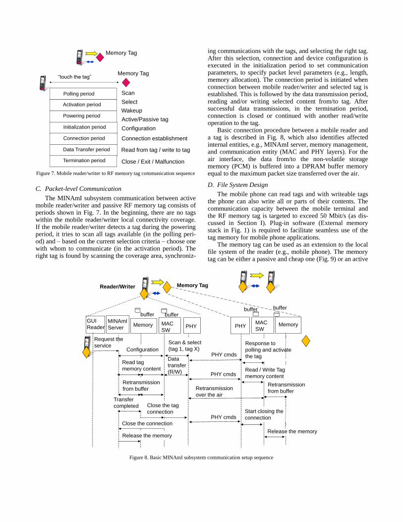
C. Packet-level Communication
The MINAmI subsystem communication between active mobile reader/writer and passive RF memory tag consists of periods shown in Fig. 7. In the beginning, there are no tags within the mobile reader/writer local connectivity coverage. If the mobile reader/writer detects a tag during the powering period, it tries to scan all tags available (in the polling peri-od) and – based on the current selection criteria – choose one with whom to communicate (in the activation period). The right tag is found by scanning the coverage area, synchroniz-
ing communications with the tags, and selecting the right tag. After this selection, connection and device configuration is executed in the initialization period to set communication parameters, to specify packet level parameters (e.g., length, memory allocation). The connection period is initiated when connection between mobile reader/writer and selected tag is established. This is followed by the data transmission period, reading and/or writing selected content from/to tag. After successful data transmissions, in the termination period, connection is closed or continued with another read/write operation to the tag.
Basic connection procedure between a mobile reader and a tag is described in Fig. 8, which also identifies affected internal entities, e.g., MINAmI server, memory management, and communication entity (MAC and PHY layers). For the air interface, the data from/to the non-volatile storage memory (PCM) is buffered into a DPRAM buffer memory equal to the maximum packet size transferred over the air.
D. File System Design
The mobile phone can read tags and with writeable tags the phone can also write all or parts of their contents. The communication capacity between the mobile terminal and the RF memory tag is targeted to exceed 50 Mbit/s (as dis-cussed in Section I). Plug-in software (External memory stack in Fig. 1) is required to facilitate seamless use of the tag memory for mobile phone applications.
The memory tag can be used as an extension to the local file system of the reader (e.g., mobile phone). The memory tag can be either a passive and cheap one (Fig. 9) or an active
Figure 7. Mobile reader/writer to RF memory tag communication sequence
Memory Tag“touch the tag”
Polling period
Activation period
Powering period
Initialization period
Connection period
Data Transfer period
Termination period
Scan
Select
Wakeup
Active/Passive tag
Configuration
Connection establishment
Read from tag / write to tag
Close / Exit / Malfunction
Memory Tag
Figure 8. Basic MINAmI subsystem communication setup sequence
Memory Tag
Memory MAC
SW
Reader/Writer
PHY
Request the
serviceConfiguration
PHY cmds
Read tag
memory content
Data
transfer
(R/W) PHY cmds
Transfer
completed
PHY cmds
Retransmission
over the air
Retransmission
from buffer
buffer bufferbuffer buffer
Release the memory
MINAmI
Server
GUI
Reader PHYMAC
SWMemory
Close the tag
connection
Close the connection
Scan & select
(tag 1, tag X)Response to
polling and activate
the tag
Read / Write Tag
memory content
Start closing the
connection
Release the memory
Retransmission
from buffer
one, including an own power source and thus being more expensive (Fig. 10) [11]. Plug-in software in the file system of the reading device handles the connection to the memory tag. Storage space on the memory is mounted on the local file system in the same way as any detachable storage. The volatile nature of the connection causes overhead in main-taining the file system view in the reader/writer device. This kind of RF memory tag would be suitable for e.g., a concert ticket containing implanted multimedia available to be read with a mobile device.
Adding a processing element to the memory simplifies the connection. An ultra low-power processing element can process the access requests independently and even provide some more advanced services like metadata-based queries [34]. A service proxy relays the service interface of the memory directly to the applications running on the accessing device. The volatile nature of the connection is not a problem
if the server is made stateless and transactions atomic. This type of RF memory tag will be able to support more complex use cases.
Device internal modules need to support NoTA to get full benefit of subsystem independency and still give a fast con-nection between subsystems. This interconnect architecture allows future extensions for modules within one device.
IV. WIRELESS INTERNET ACCESS
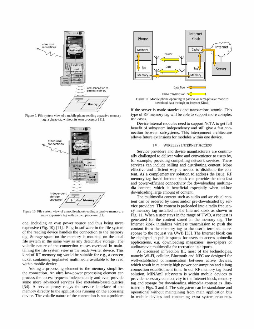
Service providers and device manufacturers are continu-ally challenged to deliver value and convenience to users by, for example, providing compelling network services. These services can include selling and distributing content. More effective and efficient way is needed to distribute the con-tent. As a complementary solution to address the issue, RF memory tag based internet kiosk can provide the ultra-fast and power-efficient connectivity for downloading multime-dia content, which is beneficial especially when ad-hoc downloading large amount of content.
The multimedia content such as audio and /or visual con-tent can be ordered by users and/or pre-downloaded by ser-vice providers. The content is preloaded into a radio frequen-cy memory tag installed in the Internet kiosk as shown in Fig. 11. When a user stays in the range of UWB, a request is generated for the content stored in the memory tag. The Internet kiosk initializes wireless transmission to push the content from the memory tag to the user’s terminal in re-sponse to the request via UWB [35]. The Internet kiosk can be deployed in public spaces for users to access ubimedia applications, e.g. downloading magazines, newspapers or audio/movie multimedia for recreation in airports.
As discussed in Section III, most of the technologies, namely Wi-Fi, cellular, Bluetooth and NFC are designed for well-established communication between active devices, which result in relatively high power consumption and a long connection establishment time. In our RF memory tag based solution, MINAmI subsystem is within mobile devices to provide necessary connectivity to the Internet kiosk, memory tag and storage for downloading ubimedia content as illus-trated in Figs. 3 and 4. The subsystem can be standalone and operational without maintaining from main application bus in mobile devices and consuming extra system resources.
Figure 9. File system view of a mobile phone reading a passive memory
tag: a cheap tag without its own processor [11].
Figure 10. File system view of a mobile phone reading a passive memory: a
more expensive tag with its own processor [11].
Figure 11. Mobile phone operating in passive or semi-passive mode to
download data through an Internet Kiosk.
Data flow
Radio transmission
Phone
Tag
Memory
Memory
Power
Data Tag
Memory
InternetKiosk
CacheInternet
Server

Besides, the subsystem can be powered off until a new re-quest arrives and it would not suffer from long latency in establishing a new connection.
In this architecture, the mobile devices could operate in either semi-passive or passive mode instead of active mode. The downloading is powered by phone battery in semi-passive mode and it is powered by the Internet kiosk in passive mode. By running in passive mode, the memory tag is powered by the Internet kiosk, and the mobile devices only consume energy to receive content and write these data into memory. This yields a great potential of energy saving on mobile devices especially when downloading large amount of content.
From the communications point-of-view, under the end-to-end Transmission Control Protocol – Internet Protocol TCP/IP layer there is a memory connection (MEMCON) layer connecting the content of the phone tag and the kiosk tag (see Fig. 12). The memory within the tags is divided into at least two parts, of which one is outgoing and one incoming data area. The master device (in the case of the kiosk, the kiosk tag) reads automatically the data in the outgoing data area of the slave device (phone tag), copying it to the incom-ing data area of its own memory. The data is then read by the controlling software and possible application level com-mands (e.g., fetch content from web address) found are then carried out. The reply data (e.g., data fetched from the web address) is then written to the outgoing data area of the kiosk tag, which is automatically copied to the incoming data area of the phone tag. Thus the memory connection layer auto-matically reads and copies the outgoing data from each de-vice to the incoming data area of the other device. The upper layer control software of each device then moves the data further to the Internet services (Kiosk) or phone memory (phone) to be used by the application requesting the data. From the point-of-view of an application on the phone re-questing data (e.g., Internet message access protocol (IMAP) email download) from a service provider in the Internet, there is a TCP/IP connection available.
The solution also makes possible providing an instant content download possibility by preloading data from an Internet service to the phone, e.g., a web page, digital maga-zine, or email account contents. In that case, the kiosk can be
labeled with the logo of the corresponding service, telling the user what he/she would get by touching the logo with the phone. As the data is pre-loaded to the tag, the speed of de-livery is only affected by the speed of the UWBLEE connec-tion and data handling and displaying within the phone.
A. Comparisons
Maximized throughput and minimized power consump-tion are critical requirements in order to extend battery life of mobile devices. Given the scenario of Internet Kiosks, vari-ous radio technologies could be utilized to provide Internet connectivity from mobile phones to the Internet Kiosks. Normally, Wi-Fi and femtocell focus on local coverage. They are widely deployed and typically used by mobile devices. However, they are not always the most viable solu-tions. When traveling abroad, data roaming over cellular network, such as 3G (WCDMA) may be very expensive.
3G and Wi-Fi typically drain battery quickly on mobile devices. Since the fixed overhead of transmission is signifi-cantly high when the radio interfaces are in communication state. Once the radio interface is on and operates in active state, most of the power is consumed on circuits and does not matter how many data are sent or received over the interface. Especially in 3G networks, the radio switches to the higher power states, DCH (Dedicated Channel) or FACH (Forward Access Channel) from IDLE state, when the network is ac-
Phone stack Embedded tag Kiosk tag Internet
Phone
memoryContent
TCP/IP
Buffer Buffer
HTTP
UI/APP
NET
MAC
PHY
NET
MAC
PHY
MEMCON MEMCON
HTTP
OUT
IN
IN
OUT
UWBLEE
TCP/IP
I-UWB
Figure 12. Schematic layout of the communication system when a mobile phone connects to the Internet via a memory-tag-based Internet kiosk.
TABLE II. COMPARISON OF POWER CONSUMPTION OF DIFFERENT
DATA COMMUNICATION TECHNOLOGIES
Wireless
interface
Max
data
rate
Maximum
application
throughput
Power
consumption
Energy
consumption
Mbit/s mW nJ/bit
3G 7.2 ~5 ~850 ~170
IEEE
802.11g 54 ~20 ~500 ~25
Bluetooth
2.0+ EDR 3 ~2.1 ~60 ~28
NFC 6.78 848 kbit/s ~30 ~35
UWBLEE 112 ~50 ~5.4 50-60 pJ/bit (*
*) The value 50-60 pJ/bit is only for the RF front-end of UWBLEE

tive [36]. Based on our measurements on a Nokia N900 phone, IDLE state is considered as low power states, which consume only around 30 mW. The state of Cell FACH con-sumes around 400 mW and the state of Cell DCH consumes around 800 mW. According to 3GPP standard, there are so called inactivity timers managed by the radio network con-troller (RNC). The transitions between the different states are controlled by inactivity timers. Transitioning from the high to the low power state immediately after a packet is transmit-ted, the device transitions only when the network has been inactive for the length of the inactivity timer. This mecha-nism serves two benefits: 1) it alleviates the delay incurred in moving to the high power state from the idle state, and 2) it reduces the signaling overhead incurred due to channel allo-cation and release during state transitions. Since lingering in the high power state also consumes more energy, network operators set the value of the inactivity timer based on this performance/energy trade-off, with typical values being several seconds long. However, these timers result in extra energy consumption even if there is no data to be sent or received since the radio has to wait for the timers to expire. The energy consumption is defined as tail energy [36].
To overcome energy consumption constraint in 3G and WLAN networks, short-range radio communication could be used. There are several radio technologies that can be con-sidered for the use of Internet Kiosks. For instance, Blue-tooth, NFC and UWBLEE where the mobile phone could operate in semi-passive mode in which communications are powered by the Internet Kiosk.
In order to reduce power consumption and extend battery
life of mobile phones, battery-operated devices require be-
ing equipped with a radio technology with high bandwidth
and low power consumption. Therefore, the mentioned radio
technologies are taken into consideration of comparison.
The transmission rate and energy consumption of receiving
data over various radios are benchmarked in Table II. Considering the scenario shown in Section I, which as-
sumes a mobile user downloads 50 MB movie trailer, Fig. 13 demonstrates the time and energy consumption of using various radio technologies. In the figure, the value of time is shown in the left y-axis and the value of energy consumption in the right. In the results of the case in 3G, data rate follows High-Speed Downlink Packet Access (HSDPA) Category 10 in 3
rd Generation Partnership Project (3GPP) Release 5 and
we assumed inactivity timer lasts 5 seconds. For the
UWBLEE technology the estimated total power consump-tion for the complete integrated transceiver with digital parts in passive and semi-passive operating modes is multiplied with the factor of 2 in comparison to the power consumption of RF front-end implementation [30]. However, the power consumption of digital parts is highly dependent on the total complexity allowed in passive and semi-passive operating modes, and on the optimized design of integrated circuit. The energy consumption does not include the part of writing data into memory storage in all the cases and only shows the energy consumption of receiving data via different radios. The power consumption of writing in our NoTA-based solu-tion is around 2 nJ/bit for NAND flash and approximate 1–2 nJ/bit for PCM. Both of memories are considered competi-tive from energy efficiency point-of-view [37].
Based on the calculation, the time spent on downloading
the movie trailer is only 8 s and the energy consumption of
RF front-end is 0.043 J when using UWBLEE. As men-
tioned, in the total power consumption for the complete
integrated transceiver the power consumption of digital
parts must be taken into account. In addition, there is a great
difference in the global power consumption of the system in
the passive and semi-passive modes although the power
consumption of the functions in the mobile phone is equal in
the two modes. The reason for this is that in the passive
mode the energy for communication is transferred wireless-
ly, whereas in the semi-passive mode the energy is taken
from the battery. The efficiency of the WPT link, mandatory
in the passive mode, is highly dependent on the factors such
as transfer frequency, size of antennas, and distance, and it
is obviously lower than in battery-powered case. Neverthe-
less, the estimated total energy consumption of downloading
the trailer remains below 0.1 J (and below 1 J with the
memory access) for UWBLEE in the mobile phone. Com-
paring other technologies with UWBLEE, the energy con-
sumption of using 3G is up to 72.25 J, where the tail energy
accounts for 6% of total energy consumption. Moreover,
time consumed on downloading the movie trailer by using
Bluetooth and NFC is up to 190.5 s and 417.7 s respective-
ly. No matter from speed and energy saving point of view,
our RF memory tag based solution would enable shorter
time of downloading ubimedia content, better user experi-
ence, as well as smaller energy consumption.
V. DISCUSSION AND CONCLUSIONS
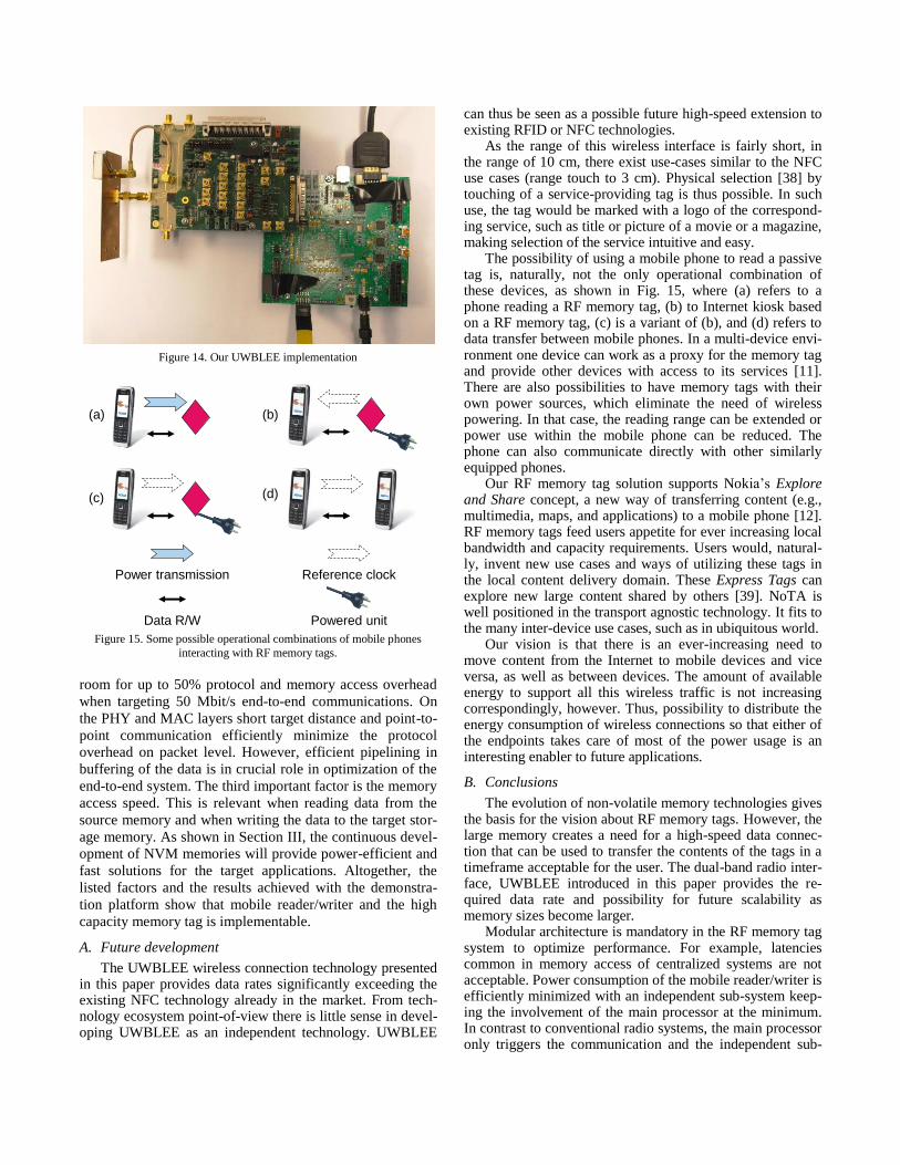
The RF memory tag (i.e., mobile reader/writer and tag)
solution was developed and tested in the MINAmI project.
Implementation is shown in Fig. 14. The development of a
RF memory tag sub-system of MINAmI project is based on
a flexible, field-programmable gate array (FPGA) based
hardware platform. The sub-system takes benefit from the
ultra-low power UWBLEE transceiver architecture, which is
suitable for data rates required in RF memory tag applica-
tions. The technical results are promising and useful for the
concept of mobile-phone-readable RF memory tags. The
data-rate of 112 Mbit/s has been achieved over the novel
radio interface in technical demonstrations [30]. This leaves
Figure 13. Time and energy consumed of using different radio technologies
when downloading 50MB movie trailer.
0
25
50
75
100
0
50
100
150
200
3G Wi-Fi Bluetooth NFC UWE
En
erg
y c
on
su
mp
tio
n /
J
Tim
e /
s
Time
Energy
Incl. energy tail
Up to 471.7 s
Only 86 mJ
room for up to 50% protocol and memory access overhead
when targeting 50 Mbit/s end-to-end communications. On
the PHY and MAC layers short target distance and point-to-
point communication efficiently minimize the protocol
overhead on packet level. However, efficient pipelining in
buffering of the data is in crucial role in optimization of the
end-to-end system. The third important factor is the memory
access speed. This is relevant when reading data from the
source memory and when writing the data to the target stor-
age memory. As shown in Section III, the continuous devel-
opment of NVM memories will provide power-efficient and
fast solutions for the target applications. Altogether, the
listed factors and the results achieved with the demonstra-
tion platform show that mobile reader/writer and the high
capacity memory tag is implementable.
A. Future development
The UWBLEE wireless connection technology presented in this paper provides data rates significantly exceeding the existing NFC technology already in the market. From tech-nology ecosystem point-of-view there is little sense in devel-oping UWBLEE as an independent technology. UWBLEE
can thus be seen as a possible future high-speed extension to existing RFID or NFC technologies.
As the range of this wireless interface is fairly short, in the range of 10 cm, there exist use-cases similar to the NFC use cases (range touch to 3 cm). Physical selection [38] by touching of a service-providing tag is thus possible. In such use, the tag would be marked with a logo of the correspond-ing service, such as title or picture of a movie or a magazine, making selection of the service intuitive and easy.
The possibility of using a mobile phone to read a passive tag is, naturally, not the only operational combination of these devices, as shown in Fig. 15, where (a) refers to a phone reading a RF memory tag, (b) to Internet kiosk based on a RF memory tag, (c) is a variant of (b), and (d) refers to data transfer between mobile phones. In a multi-device envi-ronment one device can work as a proxy for the memory tag and provide other devices with access to its services [11]. There are also possibilities to have memory tags with their own power sources, which eliminate the need of wireless powering. In that case, the reading range can be extended or power use within the mobile phone can be reduced. The phone can also communicate directly with other similarly equipped phones.
Our RF memory tag solution supports Nokia’s Explore and Share concept, a new way of transferring content (e.g., multimedia, maps, and applications) to a mobile phone [12]. RF memory tags feed users appetite for ever increasing local bandwidth and capacity requirements. Users would, natural-ly, invent new use cases and ways of utilizing these tags in the local content delivery domain. These Express Tags can explore new large content shared by others [39]. NoTA is well positioned in the transport agnostic technology. It fits to the many inter-device use cases, such as in ubiquitous world.
Our vision is that there is an ever-increasing need to move content from the Internet to mobile devices and vice versa, as well as between devices. The amount of available energy to support all this wireless traffic is not increasing correspondingly, however. Thus, possibility to distribute the energy consumption of wireless connections so that either of the endpoints takes care of most of the power usage is an interesting enabler to future applications.
B. Conclusions
The evolution of non-volatile memory technologies gives the basis for the vision about RF memory tags. However, the large memory creates a need for a high-speed data connec-tion that can be used to transfer the contents of the tags in a timeframe acceptable for the user. The dual-band radio inter-face, UWBLEE introduced in this paper provides the re-quired data rate and possibility for future scalability as memory sizes become larger.
Modular architecture is mandatory in the RF memory tag system to optimize performance. For example, latencies common in memory access of centralized systems are not acceptable. Power consumption of the mobile reader/writer is efficiently minimized with an independent sub-system keep-ing the involvement of the main processor at the minimum. In contrast to conventional radio systems, the main processor only triggers the communication and the independent sub-
Figure 14. Our UWBLEE implementation
Figure 15. Some possible operational combinations of mobile phones
interacting with RF memory tags.
Power transmission Reference clock
Data R/W Powered unit
(a) (b)
(c) (d)

system handles the transfer and storage of the data. Thus, the main processor does not have to be involved in the low level communication processes.
In addition to the RF memory tag reader/writer capability in mobile devices, mobile devices can be also equipped with embedded RF memory tags. This enables a new usage sce-nario called internet kiosk which can be further used to ena-ble internet connection seemingly with zero power consump-tion in the mobile device.
ACKNOWLEDGMENT
We thank all the partners of MINAmI project, who have contributed to development of this technology. This study is a part of MINAmI project under EU FP6 contract IST-034690. This research was also supported by the Finnish Academy under grant no 129446.
REFERENCES
[1] I. Jantunen, J. Hämäläinen, T. Korhonen, H. Kaaja, J. Jantunen, and S. Boldyrev, "System architecture for mobile-phone-readable RF memory tags". Proc. UBICOMM 2010. IARIA, 2010, pp. 310–316.
[2] V. Wu, M. Montanari, N. Vaidya, and R. Campbell, “Distributed RFID tag storage infrastructure”. University of Illinois at Urbana-Champaign, IL, USA. Tech. Rep. 2009.
[3] N. Ahmed, R. Kumar, R.S. French, and U. Ramachandran, ”RF2ID: a reliable middleware framework for RFID deployment”. Proc. IPDPS 2007. IEEE, 2007, pp 1–10.
[4] C. Ying, “A verification development platform for UHF RFID reader”. Proc. CMC'09. IEEE, 2009, pp. 358–361.
[5] N. Pillin, N. Joehl, C. Dehollain, and M.J. Declercq, “High data rate RFID tag/reader architecture using wireless voltage regulation”. Proc. RFID 2008. IEEE, 2008, pp. 141–149.
[6] J.T.E. McDonnell, J. Waters, W.W. Loh, R. Castle, F. Dickin, H. Balinsky, and K. Shepherd, “Memory Spot: A Labeling Technology”. IEEE Pervas. Comput., vol. 9, 2010, pp. 11–17.
[7] J. Nielsen, “Usability engineering”. Morgan Kaufmann, 1993.
[8] W. Cui, P. Ranta, T.A. Brown, and C. Reed, “Wireless video streaming over UWB”. Proc. ICUWB 2007. IEEE, 2007, pp.933–936.
[9] H. Witschnig, C. Patauner, A. Maier, E. Leitgeb, and D. Rinner, “High speed RFID lab-scaled prototype at the frequency of 13.56 MHz”. Elektrotechnik & Informationstechnik, vol. 124, 2007, pp. 376–383.
[10] J. Jantunen, I. Oliver, S. Boldyrev, and J. Honkola, ”Agent/space-based computing and RF memory tag interaction”. Proc. IWRT 2009. INSTICC PRESS, 2009, pp. 27–38.
[11] E. Kaasinen, M. Niemelä, T. Tuomisto, P. Välkkynen, I. Jantunen, J. Sierra, M. Santiago, and H. Kaaja, “Ubimedia based on readable and writable memory tags”. Multimedia Syst., vol. 16, 2010, pp. 57–74.
[12] M. Cooper, “Explore and Share – Nokia shows ultra-fast wireless data transfer concept”. Nokia Conversations, 23 Feb 2010.
[13] “The PayKiosks Opportunity”. PayKiosks Internet Terminals, 2011.
[14] A. R. Brisebois and R.Klein. “Enterprise femto based kiosk”. US Pat. App. 20100318417. 16 Dec. 2010.
[15] Bluetooth Kiosk System Project. webee.technion.ac.il /labs/comnet/Info/projects/winter08/cn02w08 12.1.2012
[16] K. Ok. V. Coskun, M.N. Aydin, and B. Ozdenizci, “Current Benefits and Future Directions of NFC Services”. Proc. ICEMT 2010. IEEE, 2010, pp. 334–338.
[17] www.fp6-minami.org 12.1.2012
[18] I. Jantunen, H. Laine, P. Huuskonen, D. Trossen, and V. Ermolov, “Smart sensor architecture for mobile-terminal-centric ambient intelligence”. Sens. Actuators A, vol. 142, 2008, pp. 352–360.
[19] Y. Têtu, I. Jantunen, B. Gomez, and S. Robinet, “Mobile-phone-readable 2.45GHz passive digital sensor tag”. Proc. RFID 2009. IEEE, 2009, pp. 88–94.
[20] K. Kronlöf, S. Kontinen, I. Oliver, and T. Eriksson, “A Method for Mobile Terminal Platform Architecture Development”. Advances in Design and Specification Languages for Embedded Systems, S.A. Huss, ed. Springer, 2007, pp. 285–300.
[21] projects.forum.nokia.com/NoTA/wiki 12.1.2012
[22] K. Keinänen, J. Leino, and J. Suomalainen, “Developing keyboard service for NoTA”. VTT, Espoo, Finland. Tech. Rep. 2008.
[23] www.mipi.org 12.1.2012
[24] “Open Modem Interface Proposal Based on Device Interconnect Protocol Version 1.0”. Nokia, Espoo, Finland. White paper, 2010.
[25] D. Truscan, J. Lindqvist, J. Lilius, I. Porres, T. Eriksson, J. Rakkola, and A. Latva-Aho, “Testable Specifications of NoTA-based Modular Embedded Systems”. Proc. ECBS 2008. IEEE, 2008, pp. 375–383.
[26] S. Asthana, and D.N. Kalofonos, “The problem of Bluetooth pollution and accelerating connectivity in Bluetooth ad-hoc networks”. Proc. PerCom 2005. IEEE, 2005, pp. 200–207.
[27] J. Jantunen, A. Lappeteläinen, J. Arponen, A. Pärssinen, M. Pelissier, B. Gomez, and J.A. Keignart, “New symmetric transceiver architecture for pulsed short-range communication”. Proc. GLOBECOM 2008. IEEE, 2008, pp. 1–5.
[28] S.R. Aedudodla, S. Vijayakumaran, and T.F. Wong, “Timing acquisition in ultra-wideband communication systems”. IEEE T. Veh. Technol., vol. 54, 2005, pp. 1570–1583.
[29] M. Pelissier, B. Gomez, G. Masson, S. Dia, M. Gary, J. Jantunen, J. Arponen, and J. Varteva, “112Mb/s full duplex remotely-powered impulse-UWB RFID transceiver for wireless NV-memory applications”. Proc. VLSIC 2010. IEEE, 2010, pp. 25–26.
[30] M. Pelissier, J. Jantunen, B. Gomez, J. Arponen, G. Masson, S. Dia, J. Varteva, and M. Gary, "A 112 Mb/s Full Duplex Remotely-Powered Impulse-UWB RFID Transceiver for Wireless NV-Memory Applications," IEEE J. Solid-St. Circ., vol.46, 2011, pp. 916–927.
[31] G.W. Burr, B.N. Kurdi, J.C. Scott, C.H. Lam, K. Gopalakrishnan, and R.S. Shenoy, “Overview of candidate device technologies for storage-class memory”. IBM J. Res. Dev., vol. 52, 2008, pp. 449–464.
[32] “Intel, STMicroelectronics deliver industry's first phase change memory prototypes”. Physorg.com, 6 Feb 2008.
[33] Z. Shelby, P. Mahonen, J. Riihijärvi, O. Raivio, and P. Huuskonen, “NanoIP: the zen of embedded networking”. Proc. ICC’03. IEEE, 2003, vol. 2, pp. 1218–1222.
[34] J. Arponen, A. Lappeteläinen, J. Jantunen, and O. Tyrkkö, ”Content storing device query”. US Pat. App. 20080281787. 13 Nov 2008.
[35] S. Boldyrev, I. Oliver, J. Jantunen, J. Arponen, and S. Balandin. “Method and apparatus for retrieving content via a service endpoint”. US Pat. App. 20110055351. 3 Mar 2011.
[36] N. Balasubramanian, A. Balasubramanian, and A. Venkataramani, “Energy Consumption in Mobile Phones: A Measurement Study and Implications for Network Applications”. Proc. IMC’09. ACM, 2009, pp. 280–293.
[37] S. Eilert, M. Leinwander, and G. Crisenza, “Phase Change Memory: A New Memory Enables New Memory Usage Models”. Proc. IMW’09. IEEE, 2009, pp. 1–2.
[38] P. Välkkynen, M. Niemelä, and T. Tuomisto, “Evaluating touching and pointing with a mobile terminal for physical browsing”. Proc. NordiCHI’06. ACM, 2006, pp. 28–37.
[39] S. Constantinescu, “Nokia Research Center working on high speed NFC enabled file transfers”. Intomobile.com, 9 June 2011.