synthesisandcharacterization ofcds se 1...
TRANSCRIPT

SYNTHESIS AND CHARACTERIZATION OF CdSxSe1-x/ZnS ALLOY CORE/SHELL
NANOCRYSTALS: PHOTOLUMINESCENCE QUANTUM YIELD
IMPROVEMENT WITH INFLUENCE OF COMPOSITION
By
Jessica Annette Sammons
Thesis
Submitted to the Faculty of the
Graduate School of Vanderbilt University
in partial fulfillment of the requirements
for the degree of
MASTER OF SCIENCE
in
Chemistry
August, 2009
Nashville, Tennessee
Approved:
Sandra J. Rosenthal, Ph.D.
Timothy P. Hanusa, Ph.D.

ii
ACKNOWLEDGEMENTS
I would like to thank the following people:
My advisor, Dr. Sandra J. Rosenthal, for the allowing me the opportunity to conduct
research on this project.
Professors Charles Lukehart, Timothy Hanusa and Bridget Rogers, for their
additional help and support.
Professor Anthony B. Hmelo, for training and guidance with the Rutherford
Backscattering experiment.
Albert Dukes III, for the providing me the idea of shelling alloy nanocrystals.
All members of the Rosenthal research group, especially Dr. Nathaniel Smith, Dr.
James McBride, Albert Dukes, Michael Schrueder, Jerry Chang, Becky Ordnoff, and M.
Danielle Garrett for their help, advise, and friendship.
Funding for this work was provided by several Teaching Assistantships from
Vanderbilt University and grants from the Department of Energy.

iii
TABLE OF CONTENTS
Page
ACKNOWLEDGEMENTS.................................................................................... ii
LIST OF FIGURES .................................................................................................v
Chapter
I. INTRODUCTION .......................................................................................1 1.1 Overview..........................................................................................1 1.2 Quantum Confinement in Semiconductor Nanocrystals..................3 1.3 Shelling ............................................................................................4 1.4 CdSxSe1-x Alloys ..............................................................................5 1.5 Concluding Remarks........................................................................7
II. EXPERIMENTAL.......................................................................................8
2.1 CdSxSe1-x Alloy Synthesis ...............................................................8 2.1.1 CdSe, CdS, and CdSxSe1-x Synthesis ...................................8
2.2 Core/Shell Synthesis ......................................................................10 2.2.1 CdSxSe1-x/ZnS Core/Shell Synthesis .................................10
2.3 Characterization .............................................................................11 2.3.1 Static Absorption ...............................................................11 2.3.2 Static Emission and Fluorescence Quantum Yield............12 2.3.3 Transmission Electron Microscopy (TEM) .......................13 2.3.4 Rutherford Backscattering Spectroscopy...........................13
III. RESULTS AND DISCUSSION................................................................16
3.1 Introduction....................................................................................16 3.2 Results and Discussion ..................................................................17 3.3 Conclusion .....................................................................................24
Appendix
A. Core Modifications of CdSe Nanocrystals: Manganese Doping ...............26
A.1 Manganese Doping ........................................................................26 A.1.1 Difficulty in Manganese Doping of CdSe
Nanocrystals.......................................................................27 A.2 Synthesis and Characterization of Mn:CdSe .................................28

iv
A.2.1 Synthesis of Mn:CdSe........................................................28 A.2.2 Characterization .................................................................30
A.3 Results and Discussion ..................................................................31 A.3.1 Early Synthesis and Preliminary Characterization ............31 A.3.2 Early Synthesis subjected to Growth Solution...................33 A.3.3 Selenium Heavy Synthesis and Characterization ..............35
A.3.3.1 RBS of Selenium Heavy Synthesis.....................36 A.3.3.2 TEM and EELS of Selenium Heavy
Synthesis .............................................................37 A.3.3.3 EPR of Selenium Heavy Synthesis .....................39 A.3.3.4 RBS of Selenium Heavy Synthesis: Second
Wash Series.........................................................40 A.4 Conclusion .....................................................................................41 A.5 Concluding Remarks......................................................................42
B. Surface Modifications of Ultrasmall CdSe Nanocrystals ..........................43
B.1 Synthesis and Surface Modifications.............................................44 B.1.1 Ultrasmall CdSe Nanocrystals Synthesis...........................44 B.1.2 Ligand exchange of Ultrasmall CdSe Nanocrystals ..........45 B.1.3 Shelling Ultrasmall CdSe Nanocrystals with ZnS.............46 B.1.4 Characterization .................................................................46
B.2 Results and Discussion ..................................................................46 B.2.1 Ligand Exchange of Ultrasmall CdSe Nanocrystals..........46 B.2.2 Shelling Ultrasmall Nanocrystals with ZnS.......................50
B.3 Conclusion .....................................................................................51 REFERENCES ......................................................................................................53
v
LIST OF FIGURES
Figures Page
1.1 Illustration of quantum confinement in CdSxSe1-x nanocrystals ..............................1 1.2 Illustration of quantum confinement in CdSe nanocrystals.....................................3 3.1 Absorption spectra of CdSxSe1-x of varying composition......................................17 3.2 Emission spectra of CdS0.53Se0.47 before and after the shelling. ............................20 3.3 TEM image of CdS0.63Se0.37 and CdS0.63Se0.37/ZnS nanocrystals ..........................20 3.4 RBS spectra of CdSxSe1-x and CdSxSe1-x/ZnS nanocrystals ................................. 21 3.5 Plot of quantum yield of CdSxSe1-x and CdSxSe1-x/ZnS by compositions .............23 A.1 Absorption and emission spectra of early synthesis of Mn:CdSe..........................31 A.2 Photoluminescence excitation spectra of early synthesis of Mn:CdSe..................32 A.3 Absorption spectra of early synthesis of Mn:CdSe after growth solution.............34 A.4 Absorption and emission spectra of selenium heavy synthesis of Mn:CdSe.........35 A.5 RBS spectrum of nanocrystals and wash solutions of Se heavy synthesis of
Mn:CdSe ................................................................................................................36 A.6 TEM image of nanocrystals produced by Se heavy synthesis of Mn:CdSe. .........38 A.7 EPR of nanocrystals produced by of Se heavy synthesis of Mn:CdSe..................40 A.8 RBS spectrum of nanocrystals and wash solutions of second wash series............41 B.1 Absorption and emission spectra of ultrasmall nanocrystals.................................44 B.2 a) Illustration of the pinning behavior of ultrasmall nanocrystals b) Absorption and emission spectra of nanocrystals within and outside the
pinning regime .......................................................................................................47 B.3 Emission spectra of ultrasmall nanocrystals before and after ligand
exchanges...............................................................................................................49 B.4 Emission spectra of ultrasmall nanocrystals during ZnS shelling .........................50
1
CHAPTER I
INTRODUCTION
1.1 Overview
Semiconductor nanocrystals have been the focus of extensive research because of
their unique size-dependent optical and electronic properties,1-3 which are of great
fundamental and applied interest. Various applications, such as light-emitting diodes
(LEDs),4-7 photovoltaics,8, 9 single-electron resistors,10, 11 and fluorescent tags for biological
imaging.12-14, already utilize the size tunable properties that result from the quantum
confinement of the exciton within the core. A variation on the idea of binary semiconductor
nanocrystals, alloy nanocrystals (ABxC1-x) are not only size tunable but also compositionally
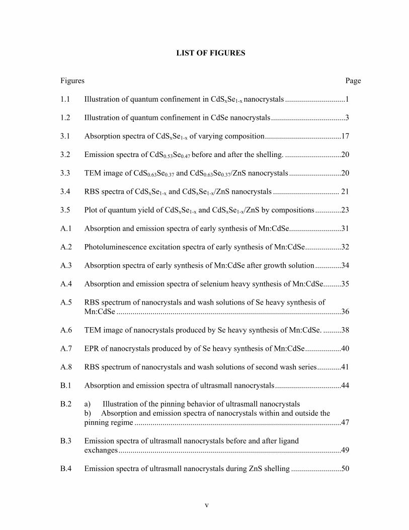
tunable materials (Figure 1.1) allowing for continuous control of their physical and optical
Figure 1.1. Illustration of quantum confinement in CdSxSe1-x nanocrystals. The dotted line represents the Bulk Bohr diameter, which decreases as the value of the variable x decreases. As the band gap energy decreases, the fluorescence of nanocrystals of similar size is seen to shift towards the red.

2
properties with the increase in the value of the variable x.15 The change in nanocrystal
constitution results in the extension of the exciton energy in the band gap of the nanocrystal,
allowing researchers to synthesize size and color tunable nanocrystals which have the ability
to access to wavelengths that are difficult to achieve with binary compounds. Alloy
nanocrystals may be the solution for applications with dual requirements, requiring small
nanocrystals in varying colors, such as in vivo imagining, multiplexing experiments16 or
photovoltaic applications.17 To date, several II-VI semiconductor alloy nanocrystals have
been synthesized: CdSxSe1-x,15 CdxZn1-xS,
18 CdxZn1-xSe,19, 20 CdSexTe1-x,
21 CdSxTe1-x22 and
HgSexS1-x.23
Lattice mismatch of the two components of the psuedobinary compound results in a
homogeneously alloyed nanocrystals that suffer from low fluorescence quantum yield. This
presents a problem for implementation and applications. An inspired solution to the problem
of low quantum yield was first reported for semiconductor nanocrystals by Hines and Guyot-
Sionnest.24 Nanocrystal cores are encapsulated by a wider band gap semiconductor material
confining electron and hole recombination to the core, eliminating fluorescence quenching
surface trap states. This process of shelling nanocrystal cores can be extended to shelling
alloy nanocrystal cores, and would prove useful in the production of high quantum yield
nanocrystals for use in future applications.
In order to increase the efficiency of the CdSxSe1-x nanocrystals and investigate the
effect of composition on photoluminescence quantum yield, this research has examined the
shelling of alloy nanocrystals of similar size and varying compositions with a wider band gap
material, ZnS. To date, there have been no reports of shelled homogeneous semiconductor

3
alloy nanocrystals (ABxC1-x). In addition to this, once the alloy nanocrystals have been
modified, there is a possibility of further functionalization for biological applications.
1.2 Quantum Confinement in Semiconductor Nanocrystals
Semiconductor nanocrystals’ optical and electronic properties are a result of the quantum
confinement of their photocreated electron-hole pairs. In bulk semiconductors, when excited,
an electron separates from the hole at a characteristic distance known as the bulk Bohr radius.
As the size of the crystal decreases below the bulk Bohr radius, the energy of the first excited
state increases, and the nanocrystal qualitatively follows particle-in-a-box behavior.25
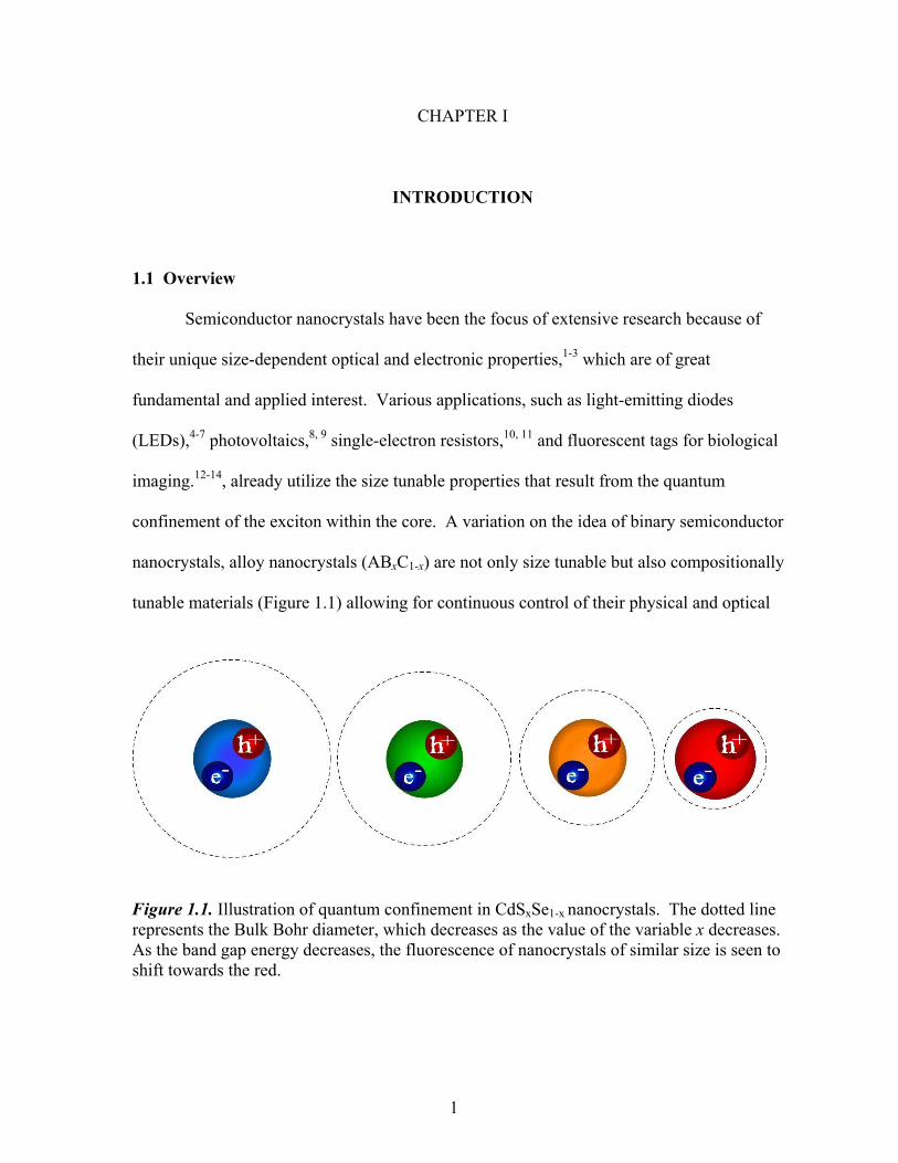
Figure 1.2. Illustration of quantum confinement in CdSe nanocrystals. The dotted line represents the Bulk Bohr diameter. As the size of the nanocrystal increases, the band gap energy decreases and the fluorescence shifts towards the red.
The energy difference between the valence and conduction band can be estimated to the first
approximation as:
∑∞
=
+−
+=
1
22
0
2
2
2
4
8.111
8 k
k
k
CdSehe
exR
S
R
e
R
e
mmR
hE α
επε (1.1)

4
where h is Plank’s constant, m is mass, and R is the nanocrystal radius, accounting for
kinetic, coulombic, and polarization energies of the electron and hole.26 The inverse square
relationship between energy and nanocrystal radius explains why as the nanocrystal increases
in size, the band gap narrows and shifts fluorescence toward redder wavelengths. In an ideal
system the energy of the photon absorbed by the nanocrystal would be equal to the energy of
the photon emitted in radiative recombination; however, energy is lost in nonradiative
processes resulting mainly from unpassivated surface atoms that act as hole traps,1 and lattice
strain from defect sites. The efficiency of radiative electron and hole recombination is
measured by quantum yield photoluminescence.
1.3 Shelling
For many applications it is desirable to produce nanocrystals with high luminescence
quantum yield. The quantum yield of pyrolytically synthesized CdSe is about 10% at room
temperature. 27 Shelling is a very useful surface modification method which drastically
improves fluorescence by growing a heteroepitaxial layer of a wide band gap semiconductor
material around a core nanocrystal, confining the electron and hole recombination to the core
and eliminating fluorescence quenching from surface trap states. In the case of CdSe
nanocrystals, ZnS is most commonly used to create CdSe/ZnS core/shells which exhibit up to
a 60% quantum yield.24 Indeed, core/shells of CdSe/CdS/ZnS have been created that can
exhibit a quantum yield of nearly 100%.28 In addition to improved photoluminescence,
shelling nanocrystals with a wider band gap material also enhances electroluminescence and
stability against photo-oxidation.24 It also acts as an encapsulant, creating a more robust

5
particle containing toxic elements such as cadmium, and allowing for surface modification
for further functionalization for use in biological applications.
1.4 CdSxSe1-x Alloys
Alloys are characterized by their combination of two or more metals, semiconductors,
or insulators, having properties differing from that of the composite pure materials. CdSxSe1-x
is a type of alloy that is known as psuedobinary, because it is composed of two compound
semiconductors, CdS and CdSe. In the same way that binary semiconductors properties
change as crystal sizes reach the nanometer scale, semiconductor alloy nanocrystals allow for
continuous tunability of their physical and optical properties through variations of the ratios
of transition metals and/or chalcogens. This allows an added degree of freedom in tuning the
nanocrystal’s properties, independent of their size, and extends the properties to that of each
characteristic binary compound and beyond. Nanocrystals that have varied amounts of two
transition metals have properties that change in a somewhat linear fashion with their
composition, while nanocrystals with varied amounts of two chalcogens (e.g. CdSxSe1-x)
sometimes have a more nonlinear dependence on the ratio, and their properties can be more
difficult to predict. Bernard and Zunger29 explained these nonlinear effects, or “optical
bowing,” by the structural and electronic effects of different atomic sizes,
electronegativities, and lattice constants of the ions involved in the semiconductor
compounds. The lattice constant, a, of CdSxSe1-x is seen to vary linearly with composition.30
CdSeCdS )1()( axxaxa −+= (1.2)
6
Meanwhile other physical properties of CdSxSe1-x alloys, such as band gap, vary nonlinearly:
)1()CdSe()1()CdS()SeCdS( x1x xbxExxEE ggg −−−+=− (1.3)
and the bowing constant, b, describes the degree of nonlinearity. Nanocrystals are
characterized by their quantum confinement, and so in addition to composition, size
dependence of the bandgap must be considered26 and when combined15 gives:
2),(),(
d
c
d
axEdxE xx
gg ++∞= (1.4)
where d is the diameter of the nanocrystal (Å), and a and c are the linear combinations of the
binary constituents.
21
21
)1(
)1(
cxxcc
axxaa
x
x
−+=−+=
(1.5)
Swafford et al.15 successfully synthesized CdSxSe1-x nanocrystals, investigated their
homogeneity and optical properties, and confirmed the tunability of the alloy nanocrystals by
size and composition. They also explored the composition dependence of the Stoke’s shift,
which changed due to nonlinear effects. Rutherford backscattering spectroscopy was used to
investigate the homogeneity as well as the composition of the alloy nanocrystals. Because
the synthesized alloys do not always have the same ratios as the original precursor mixtures,
RBS proved to be an effective method for determining the alloy stoichiometry.
7
Garrett et al.31 investigated the carrier dynamics and the effect of surface trap states
of these CdSxSe1-x alloy nanocrystals using ultrafast fluorescence upconversion spectroscopy
showing the size and composition dependent fluorescence lifetimes at the band edge which
result from the change in availability of surface trap sites and sulfur concentration.
1.5 Concluding Remarks
In this chapter, we have reviewed the basic properties of semiconductor nanocrystals,
resulting from quantum confinement, and the added degree of freedom available in alloy
nanocrystals. Shelling offers the ability to dramatically increase the fluorescence quantum
yield of conventional binary nanocrystals, and thus should be explored for improving the
quantum yield of alloy nanocrystals. In the following chapters, the synthesis of CdSxSe1-x-
/ZnS core/shells and their analysis by UV-Vis absorption spectroscopy, fluorescence
spectroscopy, RBS, and TEM to determine their size, composition, and shelling will be
described. This work is the first example of the intentional shelling of homogeneous alloy
nanocrystals. On a practical level, this opens doors for future applications by allowing
further surface functionalization of nanocrystals with higher quantum yields. On a
fundamental level, this shelling will allow further insight into origin of the optical properties
of the alloy nanocrystals.

8
CHAPTER II
EXPERIMENTAL
2.1 CdSxSe1-x Alloy Synthesis
The method of synthesizing CdSxSe1-x is discussed below in detail and was previously
described by Swafford et al.15 The cadmium source most commonly used in early binary
CdX (X= S, Se, Te) synthesis was dimethylcadmium, Cd(CH3)2, which is an expensive, air-
sensitive, toxic, pyrophoric chemical. To convert to a “greener” cadmium source, CdO has
replaced dimethylcadmium as a safer and cheaper alternative, while still producing
nanocrystals of good quality. In contrast to prevailing binary synthetic methods which use
the pyrolysis of organometallic precursors in trioctylphosphine oxide (TOPO) and
phosphonic acid,27, 32, 33 the alloy synthesis is a variation of the synthesis of Yu et al.34 which
uses oleic acid (OA) to form a Cd-oleate complex with the CdO precursor in a non-
coordinating solvent, octadecene (ODE). Nanocrystals synthesized by this method are
coated with OA as the surface ligand, and are generally of a poorer quality and have a larger
size distribution because nucleation and growth is more rapid and less controlled. However,
this synthetic technique allows for the formation of CdS, CdSxSe1-x, and CdSe and is
therefore employed for alloy synthesis.
2.1.1 CdSe, CdS, and CdSxSe1-x Synthesis
Cadmium oxide (Puratrem, CdO, 99.999%), oleic acid (OA, 90%) 1-octadecene
(ODE, 90%), tri-n-butylphosphine (TBP, tech grade 97-99%), selenium shot (200 mesh),

9
sulfur powder (Fisher, reagent grade), hexanes, toluene, butanol, ethanol, acetone, and
chloroform (all reagent grade), were purchased from Sigma-Aldrich or Strem if not otherwise
indicated and used as delivered. The cadmium precursor was prepared by combining 0.256 g
of CdO, 2.4 mL OA and 10 mL of ODE in a 100 mL three neck round-bottom flask fitted
with a temperature probe, bump trap, and a rubber septum. The reaction mixture was stirred
and purged with argon until the reaction reached 140 °C. The temperature was then raised to
310 °C and stirred until the solution became clear and colorless. For CdSxSe1-x alloy
nanocrystals, when the temperature reached 310 °C, an injection solution of 10x mL of 0.1 M
S:ODE with 10(1-x) mL of 0.1 M Se:TBP:ODE (diluted with ODE from a 4 M Se:TBP stock
solution, where x is less than 1) was swiftly injected and the temperature was reduced to 275
°C. Nanocrystals will not grow larger than approximately 36 Å in diameter without the
addition of growth solution. Aliquots were taken and diluted with toluene for subsequent
characterization. Post-synthesis isolation of the nanocrystals was carried out by precipitation
in a butanol:ethanol (1:4) mix and collected by centrifugation. The pelleted solid was
dispersed in 5 mL of chloroform and the nanocrystals precipitated by the addition of acetone
and collected by centrifugation.35 The pelleted solid containing the nanocrystals were once
again precipitated with the chloroform:acetone mix and collected by centrifugation. The
cleaned alloy nanocrystals were dispersed in hexanes for characterization. Some analysis
required cleaner nanocrystals, in which case the nanocrystals dispersed in hexanes were
precipitated out of solution by a butanol:ethanol (1:4) mix and collected by centrifugation.
This process was repeated as many as six times.

10
2.2 Core/Shell Synthesis
Even high quality, well made CdSe nanocrystals have a very low quantum yield,
ranging from 0-15%, yet many applications demand the high luminescence quantum yield.
Hines and Guyot-Sionnest were the first discover that the luminescence of such
semiconductor nanocrystals can be greatly improved by growing a heteroepitaxial layer of a
wider band gap material on a nanocrystal core.24 The first core/shells were made by growing
a layer of ZnS around CdSe cores, which improved the quantum yield of the material from
10% to 50%. The shelling layer passivates surface trap states and confines exciton
recombination to the core, resulting in more efficient radiative recombination. Recently,
advances have been made producing materials with near unity quantum yield.28 The original
synthesis used a Zn/S/TOP stock solution which used dimethylzinc(ZnMe2) and
bis(trimethylsilyl)sulfide [(TMS)2S] as the zinc and sulfur precursors, dissolved in
trioctylphosphine, TOP. In the same manner as the original nanocrystal methodologies, the
shelling procedures have been refined to exclude air sensitive chemicals and aim for a
greener and more cost effective synthesis.
2.2.1 CdSxSe1-x/ZnS Core/Shell Synthesis.
Shelling of the alloy nanocrystals was carried out following the procedure reported by
Riess et al.36 with modifications. A sample of purified nanocrystals in hexanes, 20 mL of
ODE and 6 mL of OA were combined in a 100 mL three-neck flask fitted with temperature
probe, short-path distillation apparatus, and rubber septum. The mixture is heated under
argon with stirring to 200 °C, distilling off the hexanes. When the temperature reached

11
200 °C, a solution consisting of equal volumes of 0.1M zinc napthonate:toluene, 0.1M S:di-
butyl ether, and toluene were mixed in a syringe. The ZnS solution was pumped at a
constant rate of 0.78 mL/min into the nanocrystal solution and aliquots were taken at regular
time intervals. The absorption and fluorescence measurements were monitored and addition
of the shelling solution was stopped when the fluorescence ceased to increase. Isolation of
the shelled alloy nanocrystals was carried out in the same manner as the alloy nanocrystals.
2.3 Characterization
Once the nanocrystals had been synthesized and cleaned they were characterized to
determine size, monodispersity, quantum yield, shape, and structure. Static absorption was
used to analyze the band gap energy and correspondingly the size of the nanocrystal sample
(Section 2.3.1). Static Emission was used to determine the monodispersity of the nanocrystal
sample, as indicated by the full width at half-maximum (FWHM), as well as the fluorescence
quantum yield (Section 2.3.2). Transmission electron microscopy was used to determine the
size and size distribution, as well as reveal insight as to the crystallinity of the nanocrystal
sample (Section 2.3.3). Lastly, Rutherford backscattering spectroscopy was used to
determine the elemental composition (Section 2.4.4).
2.3.1 Static Absorption
UV-visible absorption spectroscopy is an extremely useful analytical tool for
monitoring nanocrystal properties. As a result of quantum confinement in semiconductor
nanocrystals, the first excitonic peak detected by static absorption can be used to determine
the band-edge energy and consequently the nanocrystals size37 and size distribution.38

12
Nanocrystal samples were placed in a 1-cm path length cuvette and diluted in either toluene
or hexanes to an optical density of less than 1. Absorption spectra were collected from 300-
800 nm using a Varian Cary 50 UV-vis spectrophotometer. High quality nanocrystal
samples are indicated by sharper and more defined spectral features. The relationship
between the band gap, as revealed by absorption, and size has been described for binary CdS
and CdSe,37 and was found to also be nonlinearly related for CdSxSe1-x alloy nanocrystals,15
as shown in equation 1.4.
2.3.2 Static Emission and Fluorescence Quantum Yield
Fluorometry was used to collect static emission spectra, which is of particular interest
in determining the monodispersity and quantum yield of the nanocrystal samples. The
quantum yield is a measure of efficiency of radiative electron-hole recombination.
Fluorescence quantum yields are calculated by comparing the emission from a standard laser
dye to the emission from a nanocrystal sample. To prepare samples for measuring quantum
yield, the optical density (OD) of both the standard and the nanocrystal sample must be set to
less than 0.1 at the desired excitation wavelength via static absorption measurements. The
nanocrystal quantum yield can be determined using the equation:
2
2
R
R
R
Rn
n
OD
OD
I
IQQ = (2.1)
Where Q is the quantum yield, I is the integrated intensity, OD is the optical density, and n is
the refractive index of the solvent. The subscript R refers to the reference standard used, with

13
a known quantum yield. The laser dyes used were Rhodamine 6G in methanol or Coumarin
314 in ethanol depending on nanocrystal band edge.
Photoluminescence (PL) spectra were taken on an ISS PC1 photon counting
spectrofluorometer using the same sample preparation as that for absorption spectra. The PL
spectra were obtained with an excitation wavelength below the nanocrystal band edge
wavelength, and an emission range of 15 nm above the excitation wavelength to 800 nm.
2.3.3 Transmission Electron Microscopy (TEM)
High-resolution transmission electron microscopy (TEM) uses a focused electron
beam for imaging, and this technique was used on select samples to determine the size of the
nanocrystals as compared to the absorption spectra, as well as their shape and lattice order.
Because there is an accepted linear relationship between size and absorption for alloy
CdSxSe1-x,15 TEM analysis wasn’t necessary for every sample. Images were taken on a
Phillips CM20 200 kV TEM. Further details on microscope operation and sample
preparation are discussed in detail by McBride.39
2.3.4 Rutherford Backscattering Spectroscopy
Rutherford backscattering spectroscopy (RBS) is an analytical technique that uses a
high energy ion beam to bombard a sample, and measures the energy difference of
backscattered ions to determine the composition of the sample. RBS has been seen to
determine composition of nanocrystals samples to an accuracy of better than a picomole. 40
The stoichiometry of CdSxSe1-x as measured by RBS was previously reported by Swafford,15

14
and an in depth description of theory and sample preparation and evaluation have been
presented.41
Rutherford backscattering spectroscopy is able to detect atoms of different atomic
numbers, allowing each element to be identified as well as its stoichiometry. Each particle
backscatters a characteristic energy relative to the incident beam. The energy of the scattered
particles of the incident beam, E1, is related to the energy of the incident beam, E0, the mass
of the helium ions of the incident beam, m1, the mass of the target nucleus, m2, and the
scattering angle of the incident beam, θ1, by the equation:
( )
2
21
2
121
2211
01
sincos
+−±
=mm
mmmEE
θθ (2.2)
The energy of the backscattered ions is linearly related to the channel number in the RBS
spectrum, and therefore the stoichiometry of the elements can be elucidated using the ratio of
integrals of the peaks. The stoichiometry of the resulting sample can be calculated by the
equation:
( )( )
AR
BR
o
A
R
o
B
R
B
A
B
A
E
E
A
A
N
N
××=
σσ
σσ
θσθσ,
, (2.3)
where the stoichiometric ratio of element A to element B, NA/NB, is related to the integrals of
the peaks corresponding to each element, the Rutherford-pure coulomb scattering differential

15
cross section, ),( θσ ER , and a correction factor for cross sections that deviate from
Rutherford at high and low energies, Rσ
σ .
Rutherford backscattering spectrometry (RBS) was performed using a custom-built
setup.42 Nanocrystals were diluted in hexanes to an optical density of < 1.0, and dropcast on
the surface of a graphite substrate (Carbone of America), wicking to remove excess solvent.
Experiments were performed under a high vacuum (< 10-6 Torr) with a 1.8 MeV 4He ion
beam. Backscattered ions were detected at an angle of 176° Spectra were analyzed
according the procedure described by Feldman et al.43

16
CHAPTER III
RESULTS AND DISCUSSION
3.1 Introduction
Alloy nanocrystals have the potential to become the solution for biological imaging
applications with dual requirements, since they have emissions tunable by size and
composition.15 In order to utilize alloys nanocrystals they must be modified to improve the
quantum yield and allow for functionalization. By shelling the nanocrystals in a similar
fashion to that previously employed with binary nanocrystal core/shells,24 the alloy
nanocrystal core is encapsulated in ZnS. Creating an alloy core/shell serves to improve the
quantum yield of the nanocrystal while opening the possibility of further surface
modification for future applications. In addition to the practical benefit of shelling alloy
nanocrystals, it also allows an avenue through which to investigate the effect of composition
on alloy fluorescence. Garrett et al. investigated the effect of alloy composition on carrier
dynamics and found that with increasing sulfur concentration, CdSxSe1-x nanocrystals have a
larger concentration of trap states, affecting the radiative recombination fluorescence
lifetimes.44 In addition to fluorescence lifetimes, this increase in trap states affects the optical
properties of the alloy nanocrystals. Alloy core/shell nanocrystals may give information for
differentiating between the intrinsic electron trapping properties of sulfur, and surface
trapping. Sulfur’s intrinsic trapping would not be affected by the shelling layer, leading to a
less efficient core/shell, however shelling should passivate surface trapping, leading to a
more efficient and higher quantum yield material.
17
3.2 Results and Discussion
Synthesis of CdSxSe1-x nanocrystals of 30 ± 5 Å of varying compositions was
achieved using CdO in an OA:ODE mixture. Using the OA:ODE system instead of the
TOPO:HDA system yields nanocrystals with a zinc blende crystal structure rather than
wurtzite, which is essential in synthesizing the CdSxSe1-x alloy nanocrystals. This method has
previously been verified, yielding monodisperse samples of homogeneously alloyed
nanocrystals.15 However, the quantum yield of the nanocrystals synthesized in this system
(OA:ODE) is comparatively very low. This is likely due to surface trapping caused dangling
bonds or by zinc blende stacking faults and surface defects.35
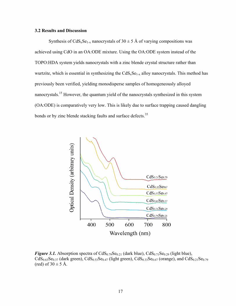
Figure 3.1. Absorption spectra of CdS0.79Se0.21 (dark blue), CdS0.71Se0.29 (light blue), CdS0.63Se0.37 (dark green), CdS0.53Se0.47 (light green), CdS0.33Se0.67 (orange), and CdS0.21Se0.79 (red) of 30 ± 5 Å.

18
The static absorption and emissions of the alloy nanocrystals were taken before shelling to
determine size and monodispersity. From the absorption maximum, the band edge was
determined and used to elucidate the nanocrystal size using equation 1.4. Absorption spectra
for CdSxSe1-x nanocrystals of approximately 30 ± 5 Å are shown in Figure 3.1. Alloy
nanocrystals displayed a typical band-edge emission peak, with deep-trap emission becoming
more apparent as the concentration of sulfur increased, as expected with increased surface
trapping. Nanocrystals with band edge emission peaks having a smooth and symmetrical line
shape with a full width at half-maximum (FWHM) of 50 nm or less were considered
adequately monodisperse and were used in the shelling experiments. Any change in the
FWHM during shelling will reflect the focusing or defocusing of the size distributions of the
alloy nanocrystals.
The need for a semiconductor with a wider band gap than both CdSe and CdS guided
the choice of ZnS as the shelling material. Indeed ZnS is a popular choice and has many
advantages for shelling CdSxSe1-x. A layer of ZnS can be added to core nanocrystals at a
temperature that doesn’t encourage core growth or ZnS nucleation. Because ZnS forms at a
lower temperature than CdS, and has a 7% lattice mismatch, while the lattice mismatch for
CdSe and ZnS is about 12%,45 there is little possibility for core/shell alloying. As a shelling
layer, ZnS effectively confines both electrons and holes to the core allowing for direct
recombination.
The absorption and emission was monitored during the shelling process. In most
cases as the shelling layer increased, the peaks in the absorption spectra did not shift a
significant amount; however they did broaden, with higher energy transitions covered by the
continuum of the band gap. This broadening is due to nonradiative processes, caused by
19
bond strain and lattice mismatch created by growth of the shell on the alloy core surface as
well as a distribution of shell thickness.46 The retention of the band edge peak in the
absorption indicates that the shelling process has not allowed for core modification or core
and shell alloying. The emission spectrum confirms that the quality of the nanocrystals
remain intact, continually displaying a narrow band edge peak. Initially the emission peak
seems to blue shift while decreasing in intensity. It is believed that the reason for this is the
initial surface rearrangement that takes place as the first layer of ZnS is added. As the
shelling layer thickens, the emission peak is seen to red shift only slightly, likely due to
partial exciton leakage into the ZnS matrix,46 while the intensity increases as much a five-
fold. This red shifting behavior has been observed in nanocrystals allowed to grow without
any shelling layer. However nanocrystal core growth is unlikely the case, during synthesis
the alloy nanocrystals were allowed to grow to the largest size possible without adding
growth solution, and a marked improvement in quantum yield not seen in nanocrystals grown
without shelling material was observed. Indeed, a similar slight red shift has been seen in
CdSe/ZnS.24, 46 An example of the alloy emissions specta before and after completion of the
shelling process is shown in Figure 3.2. The ZnS creates a heteroepitaxial layer on the
surface, quenching trap sites and confining the electron and hole to the alloy core. This leads
to an emission spectrum with greatly improved quantum yield, dominated by band edge
recombination.

20
Figure 3.2. An example of the emission spectra of CdSxSe1-x before and after the shelling process. The quantum yield of this particular sample (CdS0.53Se0.47) increases from 4.8% to 22.3% with the addition of the ZnS shelling layer. There is a slight redshift of the band edge peak due to exciton leakage into the ZnS matrix.
Figure 3.3. TEM image of CdS0.63Se0.37 and CdS0.63Se0.37/ZnS core/shell nanocrystals.

21
High resolution transmission electron microscopy images were taken to ensure that
nanocrystal samples consisted of monodisperse crystals (corroborating the emission data) and
to confirm the presence and thickness of a shelling layer. Figure 3.3 shows the TEM images
taken before and after shelling CdS0.63Se0.37 nanocrystals. The diameter increases from about
30 Å to 50 Å, indicating a shell growth of approximately 10 Å, which corresponds to 3.2
monolayers of ZnS shell.46 Samples imaged by TEM were seen to have a shelling layer of
similar thickness.
Rutherford backscattering spectroscopy was used to determine the stoichiometry of
CdSxSe1-x as well as confirm the presence of zinc for the CdSxSe1-x/ZnS core/shells. An
example of normal RBS spectra before and after shelling can be seen in Figure 3.4.
Figure 3.4. Typical RBS spectra of CdSxSe1-x (red) and CdSxSe1-x/ZnS (blue) normalized to the Cd peak. The appearance of a Zn peak and increase in the S peak qualitatively confirms shell growth. Peaks at 160 and 299 are from Oxygen, which is present on the nanocrystal surface, and Calcium, which is an impurity in the solvents used to purify the nanocrystals.
Because of reaction conditions, the stoichiometry of the synthesized nanocrystals
differs slightly from the ratios used in synthesis. The true stoichiometry of the alloy

22
nanocrystal is calculated by equation 2.3, as determined by RBS evaluation of thoroughly
cleaned samples. In addition to stoichiometry, it is also possible to calculate the average
thickness of the shelling layer of the alloy core/shell.41 Because of the different binding
energies of the nanocrystal facets the shelling does not produce an even layer encapsulating
the core, it is heteroepitaxial in nature, therefore the calculated shell thickness would only
serve as an average estimate. The presence of a very large Zn peak as well as the increase in
the S peak indicates that the expected normal shelling layer on the nanocrystal is present, but
TEM serves as a better tool for quantitatively determining shell thickness.
The success of this work is seen in the enhanced fluorescence efficiency of the
CdSxSe1-x alloy nanocrystals. The quantum yield was determined using a standard laser dye,
matching the optical density of the nanocrystal sample and dye at a specified wavelength. In
this experiment, either Rhodamine 6G in methanol or Coumarin 314 in ethanol were the
preferred laser dye standards. The photoluminescence quantum yield was calculated using
equation 2.1. Some general trends are detectable, as seen in Figure 3.5 which shows the
quantum yield before and after shelling of various compositions.

23
Figure 3.5. Scatter plot of quantum yield of CdSxSe1-x and CdSxSe1-x core/shells with varied values of x.
While the band edge emission of more sulfur heavy alloy nanocrystals is indeed less
intense than selenium heavy, the effect of increased sulfur content is the increase in alloy
core deep trap emission from surface trap states, contributing to an higher quantum yield
overall. As the shelling layer is grown surface trap states are passivated, quenching the deep
trap emission and the band edge peak is seen to dramatically increase in intensity in all
samples regardless of composition. It was expected that the quantum yield of the shelled
alloys would display a similarly increasing trend as seen in the alloy cores, as the lattice
constant of ZnS is closer to that of CdS than CdSe resulting in less lattice mismatch.
However, the quantum yield of the alloy core/shells seemed to reach a maximum at about
midway through the composition. At CdS0.5Se0.5 the crystal structure has reached the
maximum amount of structural disorder and has a lattice constant halfway in between CdS
and CdSe, after which the surface becomes dominated by sulfur dangling bonds. The
decreased improvement in quantum yield may be explained in terms of Se and S dangling

24
bond reactivity. Selenium dangling bonds are more reactive because of the smaller CdSe
band gap, and are therefore more likely to oxidize, be bound to a ligand, and in the case of
shelling, become the bond at the ZnS core/shell interface. This means that fewer Se dangling
bonds will be available for hole trapping. As the concentration of S increases, so does the
amount of potentially unpassivated bonds at the core/shell interface, which in conjunction
with shell growth preferentially forming at the Se sites, may induce lattice strain not
originally expected in comparing the lattice constants of the core and shell materials.
It has previously been seen that CdS is inherently inefficient, possessing a lower
quantum yield than normal CdSe. Sulfur acts as an intrinsic electron trap, which Garrett et al.
observed when investigating CdSxSe1-x nanocrystal fluorescence lifetimes. Shelling with a
wider band gap material would be ineffective in restoring direct radiative recombination not
caused by surface trap states. Trapping is seen in the shelling of more sulfur heavy alloys,
the quantum yield improvement decreases with increasing sulfur content.
In any case, with the addition of a ZnS capping layer there is a dramatic increase in
alloy nanocrystal quantum yield. This opens up the possibility of CdSxSe1-x use in future
applications. In particular, shelling makes alloys viable possibilities for biological imaging
applications by encapsulating toxic cadmium and allowing for further surface
functionalization.
3.3 Conclusion
This work presents the first example of alloy semiconductor nanocrystals shelled with
ZnS. The presence of the wider band gap shell formed directly on nearly monodisperse alloy
cores is established by RBS and TEM. Static absorption and emission proves the retention of

25
the initial core size. The quantum yield of the passivated alloy nanocrystals is seen to benefit,
exhibiting an unexpected trend with changing composition. In the future, these new alloy
core/shell nanocrystals may be further characterized to better understand their optical
properties, trends in quantum yield improvement, as well as their recombination kinetics.
They may also be water-solublized and functionalized for biological imaging applications
having dual requirements that would benefit from the alloy nanocrystal’s added degree of
freedom.

26
APPENDIX A
Core Modifications of CdSe Nanocrystals: Manganese Doping
Alloy semiconductor nanocrystals are compositionally tunable materials, exploiting
the properties of the binary semiconductor materials that are used to create them. A different
way to tune nanocrystals emission is to modify the core structure by doping with transition
metal ions, introducing new energy levels into the semiconductor band structure.
Furdyna et al. first investigated transition metal doped bulk semiconductors, also
called diluted magnetic semiconductors (DMS), and found that they exhibit optical properties
tunable in respect to dopant concentration.47 Only in the past decade has there been
investigation into the doping of semiconductor nanocrystals, potentially overcoming intrinsic
disadvantages such as sensitivity to thermal, chemical and photochemical disturbances, and
self-absorption.48, 49
A.1 Manganese Doping
Among the transition metals used to dope bulk DMS, paramagnetic ions such as
manganese display unique magnetic and magneto-optical properties, which result from the
sp-d exchange interaction between dopant ions and semiconductor charge carriers.50, 51
Manganese has a sharp, atomic-like emission line that is easily detectable in the visible
range, making it a logical and popular choice as a dopant ion and luminescence activator.52
In the matter of transition metal-doped II-VI nanocrystals, there have been several reports of

27
successful Mn2+ incorporation in CdS, ZnS, ZnxCd1-xS and ZnSe semiconducting
nanocrystals, and only a few reports of CdSe.48, 53-61
A.1.1 Difficulty in Manganese Doping of CdSe Nanocrystals
CdSe would be an ideal nanocrystal system to dope with Mn2+ because it is the most
understood II-VI system and has absorption and emission within the range of visible
wavelengths, making the optical properties easily detectable and useful. Manganese is
isovalent to cadmium; therefore it will not contribute any extra electrons or holes, but can
enhance the interaction between the charge carriers recombination by localizing the exciton
before nonradiative processes can occur,62 in turn improving the efficiency of the
fluorescence. Early efforts to dope Mn2+ into CdSe failed to incorporate any dopant.59
While Mn2+ is sufficiently soluble in bulk, it is resistant to incorporation into the CdSe
nanocrystal lattice. Studies to explain the difficulty of manganese doping of CdSe have been
carried out. Dalpian et al. proposed that the nanocrystals “self-purify,” pushing out the
impurities as they grow.63 This theory assumes that nanocrystal is in thermodynamic
equilibrium with its environment and that the impurity atoms are able to diffuse readily
throughout the nanocrystal. However, Mn2+ diffusion in bulk II-VI semiconductors is
negligible at liquid-phase growth temperatures, although surface diffusion may still be
facile.64 Erwin et al. utilized density-functional theory (DFT) to calculated the binding
energies of Mn2+ to CdSe facets.65 They reported that the underlying mechanism of doping is
controlled by the initial adsorption of impurities onto the nanocrystal surface during growth.
The efficiency of the adsorption is determined by the nanocrystals surface morphology,
shape, size, and the surfactants present in growth solution. They found that theoretically,
28
Mn2+ has a high binding energy to the (001) facets of zinc blende CdSe, but no binding
energy of sufficient strength to any of the wurtzite facets.
Mikulec et al. were the first to report a successful synthesis of Mn:CdSe59 by
organometallic decomposition using Mn2(µ-SeMe)2(CO)8 as a single source Mn-Se
precursor. Other methods have been used to produce Mn:CdSe, such as Atomic Layer
Epitaxy (ALE)61 and the use of inorganic cluster precursors. 60 Because of the difficulty of
CdSe doping, normal colloidal synthesis had not been reported until recently, when Kwak et
al. reported a method of doping zinc blende CdSe in a paraffin oil solvent with oleic acid as
the ligand,58 which allowed ~ 4 % Mn2+ doping. However, only the absorption spectra and
XRD were reported, which does not seem to be sufficient evidence of successful doping.
In an attempt to confirm the successful doping of CdSe with Mn2+ this appendix
discusses static absorption and emission, Rutherford backscattering spectroscopy (RBS),
high-resolution transmission electron spectroscopy (TEM), electron energy loss spectroscopy
(EELS), and electron paramagnetic resonance spectroscopy (EPR) performed on nanocrystal
samples synthesized by the colloidal method. The use of these analytical techniques should
provide a better understanding of the extent of doping than methods previously reported.
A.2 Synthesis and Characterization of Mn:CdSe
A.2.1 Synthesis of Mn:CdSe
Cadmium oxide (Puratrem, CdO, 99.999%), cadmium acetate dihydrate
(Cd(OCOCH3)2·2H2O, 98%), cadmium chloride (CdCl2, ≥99.0%), manganese acetate
(Mn(OCOCH3)2, 98%), manganese acetate tetrahydrate (Mn(OCOCH3)2·4H2O, ≥99.0%)
oleic acid (OA, 90%) 1-octadecene (ODE, 90%), selenium shot (200 mesh), hexanes,

29
toluene, butanol, ethanol, acetone, and chloroform (all reagent grade), were purchased from
Sigma-Aldrich or Strem if not otherwise indicated and used as delivered.
The procedure for doping CdSe nanocrystals with Mn2+ as submitted by Kwak et al.
was followed58 with modifications. A total of 2 mmol of Cd precursor (CdO,
Cd(OCOCH3)2·2H2O, CdCl2), 0.5 mmol Mn- precursor (Mn(OCOCH3)2,
Mn(OCOCH3)2·4H2O), 10 mL ODE, and 4 mmol OA were placed in a 100 mL threeneck
round-bottom flask and heated to 160°C purging with Ar until 150°C. The resulting solution
was clear and colorless. When cadmium precursor was completely converted, 2.5 mmol- 3
mmol of Se precursor (Se:ODE) was injected into the hot solution and allowed to grow to the
desired size. To stop growth, heat was removed and BuOH was quickly injected. Isolation
of the nanocrystals was carried out by precipitation in a butanol:ethanol (1:4) mix and
collected by centrifugation. The pelleted solid was dispersed in 5 mL of chloroform and the
nanocrystals precipitated by the addition of acetone and collected by centrifugation.35 The
pelleted solid containing the nanocrystals were once again precipitated with the
chloroform:acetone mix and collected by centrifugation after which they were subjected to
further precipitation by butanol:ethanol or chloroform:acetone as many times as necessary.
The clean nanocrystals were dispersed in hexanes or toluene for characterization, storage, or
any other future purpose.
To create larger nanocrystals, a growth solution must be added to the cleaned
nanocrystals. The solution is created by combining 0.76g of CdO, 6 mL OA, and 25 mL
ODE which is then heated to 290 °C until the solution become clear and colorless. The
solution was cooled to 50 °C and then 1.25 mL of 4M Se:TBP was added to the solution at

30
room temperature. This solution is added dropwise at a constant rate to cleaned nanocrystals
in a three-neck flask at 160 °C.
A.2.2 Characterization
Once the doped nanocrystals had been synthesized and cleaned they were
characterized to determine size, photoluminescence, monodispersity, shape, stoichiometry,
and presence of dopant ions. Static absorption (Section 2.3.1), static emission (Section 2.3.2)
transmission electron microscopy (Section 2.3.3), and Rutherford backscattering
spectroscopy (Section 2.4.4) were used for the purposes expressed as discussed in the
previous sections.
Scanning transmission electron microscope electron energy loss spectroscopy
(STEM-EELS) is used to detect the presence of manganese in the nanocrystal samples. High
resolution EELS analysis is useful for providing elemental analysis on the atomic scale. 66
Manganese is known to have a strong EELS signal, especially when in the oxidation state is
+2 and it has a paramagnetic d5 orbital arrangement.67 However, this signal may be difficult
to detect if the Mn2+ is not very concentrated in the nanocrystal.
Electron paramagnetic resonance (EPR), is used to measure the absorption of
microwave radiation of unpaired electrons in a strong magnetic field and reveals spin
interactions of bonded atoms. This allows for the detection of paramagnetic ions as well as
investigation into the nature of the dopant location. The spin interactions are sensitive to the
dopant’s local environment, whether it is bound to the surface or incorporated into the
nanocrystal.68 Manganese (Mn2+) is readily detectable by EPR because it is paramagnetic,

31
having five unpaired electrons occupying all five d-orbitals, giving a nuclear spin of I=5/2.
Splitting patterns are predicted by the equation 2I+1.
A.3 Results and Discussion
In an attempt to synthesize Mn2+ doped CdSe nanocrystals by common colloidal
pyrolysis method, reactions were carried out following the method of Kwak et al. with
modifications.58 It was found that larger nanocrystals could be synthesized using a selenium
heavy reaction.
A.3.1 Early Synthesis and Preliminary Characterization
Early efforts to synthesize Mn:CdSe nanocrystals resulted in absorption spectra with
two pronounced features at about 458 nm and 430 nm (Figure A1), regardless of the amount
of time they were allowed to grow.
Figure A1. Typical example of normalized absorption (red) and emission (blue) spectra of early synthesis of Mn:CdSe

32
The sharp, two-featured absorption is unlike previously reported spectra. If these
features are not characteristic of Mn:CdSe, they could possibly be the result of nanocrystal
seeds occurring at energetically favorable sizes, nanocrystals with abnormal shape (i.e. rods
or triangular) instead of the typical spherical shape, or of some byproduct of the reaction. If
nanocrystal seeds were produced, the corresponding emission spectrum would be expected to
show multiple peaks corresponding to nanocrystals of different sizes, however this does not
seem to be the case. Manganese in known to have an atomic-like emission line occurring at
about 580 nm, which should be observed along with band edge emission at nanocrystal sizes
less than 3.3 nm.69 Figure A1 shows the emission spectrum containing a small peak at about
467 nm, possibly the band edge peak, and a large peak at about 580 nm, indicating the
presence of Mn2+ in the nanocrystal, followed by what appears to be deep trap emission.
The PLE spectrum collected by monitoring at 580 nm mimics the absorption spectra
(Figure A2). These results have been previously observed,69 and is believed to
Figure A2. Normalized PLE excitation spectra monitoring at different wavelengths.

33
demonstrate that the Mn2+ emission is sensitized to the CdSe nanocrystal excitation and the
exciton is quenched. Interestingly, the PLE spectra collected at 625, 640, and 660 nm, all
mimic the absorption spectrum. The PLE spectrum collected by monitoring below 580 nm,
such as at 467 nm (the wavelength of the taller of the two features), did not show the origin
of the absorption features. If Mn2+ doping does the quench exciton, it is expected that the
PLE collected by monitoring below the manganese transition energy would produce a
featureless spectrum.
The broad emission to the red of the Mn2+ emission may be explained by mid gap trap
sites cause by surface defects, or by bond strain or defects of the nanocrystal lattice caused
by the substitution of Mn2+ in the crystal lattice. These lower lying levels would not be
quenched by Mn2+ doping like band edge recombination, having recognizable deep trap
behavior after 580 nm.
Preliminary RBS data determined that the nanocrystals had a detectable Mn peak.
However, it is possible that if the Mn2+ precursor has similar solubility in solvents, the Mn
detected by the RBS is in solution with the nanocrystals or loosely bound to the surface and
not incorporated in the nanocrystals.
A.3.2 Early Synthesis subjected to Growth Solution
In order to create larger nanocrystals for easier imaging and test if the unusual
absorption features were indicative of monodisperse doped nanocrystals seeds, or some other
non-emitting material, a batch of Mn:CdSe nanocrystals was injected with a CdSe growth
solution. If the nanocrystals are doped and monodisperse, it is expected that the growth
solution should act as a shelling layer, encapsulating any Mn2+ on the surface of the

34
nanocrystal, and increasing the size of the nanocrystal in solution. Figure A3 shows the
growth of the nanocrystals, one large peak appears in the absorption spectrum, indicative of a
single size of monodisperse nanocrystals. These nanocrystals may be a result of new
Figure A3. Normalized absorption of early synthesis of Mn:CdSe subjected to a growth solution at 160° C. Ideally CdSe would act as a shelling layer, encapsulating the impurities inside of the NC. Note that the features at 430 and 458 nm remain.
nucleation and growth, or of doped or undoped nanocrystals increasing in size. The two
original absorption features become less dominant, but are still present after the growth
solution has been added, however they do not move with respect to the size of the
nanocrystal. Higher order energy transitions behave in the same way as the first allowed
transition, as a “particle in a box,”25 changing in energy with respect to nanocrystal size.
Therefore, the peaks in the absorption spectra are indicative of some byproduct material that
is not subject to quantum confinement and does not shift when subjected to a CdSe growth
solution.

35
A.3.3 Selenium Heavy Synthesis and Characterization
A selenium heavy synthesis has been seen to increase the surface area of the 001
facet, the energetically favorable facet for doping with Mn2+, in Mn:ZnSe.65 A selenium
heavy synthesis for Mn:CdSe yielded more concentrated solutions of larger nanocrystals,
more quickly, and resulted in absorption spectra with one feature dependent on the growth
time. Figure A4 shows an example of the absorption and emission spectra of the selenium
heavy synthesis. The narrow emission peak has a full width half maximum (FWHM) of
about 40 nm, indicating a fairly monodisperse sample. This band edge peak is the only
feature seen in the emission spectrum because the energy of the conduction band is lower
than the Mn2+ transition, thus dominating the emission spectrum.69 Again it is noted that the
absorption features at 430 and 458 (not pictured), believed to result from some byproduct of
the reaction, are still present in the nanocrystal synthesized by the Se heavy method.
Figure A4. Typical example of normalized absorption (red) and emission (blue) spectra of selenium heavy synthesis of Mn:CdSe which yields larger NCs.
These results were more similar to what Kwak et al. found, and seemed quite
promising. Unfortunately, since no Mn2+ emission can be observed, other analytical methods

36
must be used to evaluate the samples and provide support for successful doping.
Transmission electron spectroscopy was used to image the nanocrystals and reveal their size
and morphology. Rutherford backscattering spectroscopy, EELS, and EPR were used to
determine if the nanocrystals were indeed being doped with Mn2+, and to what extent.
A.3.3.1 RBS of Selenium Heavy Synthesis
The nanocrystals from the selenium heavy synthesis were washed multiple times and
the nanocrystals as well as supernatant were evaluated using RBS (Figure A5) to determine
the dopant concentration and monitor the effectiveness of the washes in
Figure A5. Normalized RBS spectrum, with regards to Se. Nanocrystals (A) and wash solution (B)

37
removing the Mn precursor. The nanocrystals were extracted with butanol:ethanol
and additional six times after the initial purification. RBS analysis of the nanocrystals after
the final wash shows a Mn signal, and the wash solution no longer shows a Mn signal,
indicating the manganese being detected may be from doped Mn:CdSe.
Using equation 2.3, the stoichiometry of the Mn:CdSe was calculated. A doping
range of 6.7% to 28.6% was observed, generally with less than 10% relative uncertainty.
This data suggests that either the doping concentration achieved is much greater than that
reported by Kwak et al., or that all of the Mn is not being removed from solution, the latter
being much more likely. Nevertheless, this evidence encouraged further analysis to reveal
information about the location and nature of the Mn2+ dopant atom. The nanocrystals were
evaluated by TEM, EELS and to prove the incorporation of the Mn2+ dopant.
A.3.3.2 TEM and EELS of Selenium Heavy Synthesis
Transmission electron microscopy (TEM) and scanning transmission electron
microscope electron energy loss spectroscopy (STEM-EELS), were used to image and study
the Mn:CdSe semiconductor nanocrystals. TEM is a useful technique for obtaining structural
information for single nanocrystals. Figure A6 shows the TEM images of the Mn:CdSe
nanocrystals from the selenium heavy synthesis. The image shows monodisperse
nanocrystals with a diameter of about 5 nm.

38
Figure A6. TEM image of Se heavy synthesis of Mn:CdSe. NCs appear fairly monodisperse (A). Magnified portion of TEM (B) shows NC of approximately 5 nm in diameter with obvious lattice fringes. Shape and fringing are consistent with zinc blende structure.
This corresponds nicely with the absorption feature at 605 nm (Fig A4), consistent
with a nanocrystal of 4.8 nm in diameter, as calculated from previous literature.37 The
nanocrystals exhibit a triangular shape, which is commonly observed with zinc blende
nanocrystals. The triangular shape is slightly more pronounced than in normal CdSe
nanocrystal reactions, which could result from the different reactivity of the precursors and
their binding energies to the different facets.
High resolution EELS analysis is useful for providing elemental analysis on the
atomic scale. 66 Manganese is known to have a strong EELS signal, especially when in the
oxidation state is +2 and it has a paramagnetic d5 orbital arrangement.67 However, this signal
may be difficult to detect if the Mn2+ is not very concentrated in the nanocrystal. If the

39
nanocrystal synthesized by the modified Kwak et. al method have the same doping efficiency
as the previously reported Mn:CdSe, then the concentration is expected to be quite low at
only 4% (at.) or less.58 When the sample was evaluated using EELS no Mn2+ signal was
detected, indicating that the sample has very low dopant concentration or possibly no dopant
incorporation at all.
A.3.3.3 EPR of Selenium Heavy Synthesis
Another method of investigating the presence and nature of the Mn2+ bond in the
nanocrystal is measuring the absorption of microwave radiation by unpaired electrons in a
strong magnetic field by electron paramagnetic resonance (EPR). The Mn2+ ion is
paramagnetic, having five unpaired electrons occupying all five d-orbitals, giving a nuclear
spin of I=5/2. Splitting patterns are predicted by the equation 2I+1, thus predicting that Mn2+
would have a six line pattern, which is indeed a signature of Mn2+ hyperfine splitting. The
hyperfine splitting reported for Mn2+ in bulk CdSe is 62×10-4 cm-1,70 and the hyperfine
splitting for Mn:CdSe nanocrystals was found by Mikulec et. al to be 83×10-4 cm-1.59
Mikulec conjectures that the larger splitting pattern is a result of the different bonding
environments of Mn2+ loosely bound to the surface of the nanocrystal instead of in the core.
When the samples were evaluated using EPR (Figure A7), the line shape showed no
characteristic hyperfine splitting, indicating no dopant incorporation in the CdSe nanocrystal
or surface bound dopant ions.

40
Figure A7. EPR of Se heavy synthesis of Mn:CdSe. No hyperfine splitting is observed.
A.3.3.4 RBS of Selenium Heavy Synthesis: Second Wash Series
The data collected with RBS disagrees with the EELS and EPR data. It is possible
that the Mn precursor solubility in the solutions used in the first wash series was too high, so
a second wash series was performed on a new batch of nanocrystal subject to the same
doping conditions. Six additional extractions with chloroform:acetone were performed after
the initial purification. The washed nanocrystals as well as the wash solution were evaluated
using RBS (Figure A8). A disappearance of the Mn peak in the nanocrystal samples was
observed after only two washes. The wash solution continued to have Mn peaks, indicating
no Mn2+ was being doped into the CdSe, but that it was all being removed in successive

41
Figure A8. Normalized RBS spectrum, with regards to Se. Nanocrystals subjected to second wash series (A) and the second series wash solutions (B).
washes. These results indicate that the Mn precursor must be more soluble in the
chloroform:acetone mixture allowing for better removal of the Mn precursor, and cleaner
nanocrystals.
A.4 Conclusion
The selenium heavy modified synthetic method used in this work gave similar results
to that reported by Kwak et al., but after further evaluation with RBS, EELS, and EPR were

42
found to not be successfully doped. Rutherford backscattering spectroscopy is a useful tool
for determining nanocrystal stoichiometry, and it sensitive up to a picomole, however it is not
able to distinguish between dopant atoms incorporated into nanocrystals and dopant that is in
solution with the nanocrystal. EELS and EPR are able to detect nanocrystals doped with
paramagnetic manganese as well as reveal the nature of the dopant bond and location. Using
these analytical techniques it is concluded that this synthesis was not successful. However, a
wash method of additional chloroform:acetone extractions proved more effective than
previously reported methods in removing manganese precursor and ions from solution.
A.5 Concluding Remarks
CdSe is a notoriously difficult nanocrystal system to dope with Mn2+. Erwin reported
that doping depends on the size, shape, and morphology of the nanocrystals and the
surfactants present in solution.64 Pradhan et al. reported that in Mn:ZnSe, the Mn2+ precursor
should be significantly less reactive than Zn2+ if they both have the same carboxylate
ligand.62 Most certainly Cd2+ would also be a more reactive precursor. Seemingly, the
surfactants present in solution and the shape of the nanocrystal are the varying factors that
may make doping in this system difficult. A few more avenues could be explored before
abandoning this system. Precursors and surfactants of differing reactivities may provide a
more successful approach to this general system. Also, shelling with a more reactive and
stable shell, such as ZnS, may allow for the encapsulation of the Mn atoms on the surface of
the CdSe nanocrystal that may otherwise be removed during washes.

43
APPENDIX B
Surface Modifications of Ultrasmall CdSe Nanocrystals
In addition to being able to tune nanocrystal properties by core composition (i.e.
alloying and doping), it is also possible to affect photoluminescence by controlling the
surface of the particle. Optical studies indicate that surface morphology may play as
important a role in photoluminescence as crystallite size, especially in the electronic
relaxation processes.1, 33, 71 Surface studies33, 42 as well as theoretical modeling 72 agree that
the majority of CdSe nanocrystal hole traps originate from surface selenium sp3-hybridized
dangling bond orbitals, leading to charged, higher energy surfaces. Cadmium atoms
generally do not act as electron traps because of the superior passivating ability of the surface
ligands.42
As nanocrystal size decreases entering into the ultrasmall size regime, 1.7 nm and
below, the optical properties change dramatically because of the ever increasing surface area
to volume ratio. Instead of the size-dependent, strong band edge emission that is typically
observed in larger nanocrystals, the ultrasmall CdSe nanocrystals, on the order of 15 Å, are
governed by their surface states instead of band gap, producing a white-light emission. 73, 74
This broadband emission covers the wavelengths of the entire visible spectrum, and is
characterized by three trap-state emission features (Figure B1) that are size independent.75
In order to better understand the nature of the unique, size-independent properties, the
surface of the ultrasmall nanocrystals were modified and the effect of the surface change on
their optical properties observed. The surface modifications discussed in this appendix are

44
ligand exchange and shelling, and this work has been published in reports by Dukes75 and
Bowers,76 respectively.
Figure B1. Typical absorption (red) and emission (blue) spectra of ultrasmall white-light emitting nanocrystals.
B.1 Synthesis and Surface Modifications
B.1.1 Ultrasmall CdSe Nanocrystals Synthesis
Tri-n-butylphosphine (TBP, tech grade 97-99%), selenium shot (200 mesh), cadmium
oxide (Puratrem, 99.999%), hexadecylamine (HDA, tech grade, 90%), triethylphosphite,
dodecylbromide, octylbromide, hexadecylbromide, ethyl acetate, hexanes, toluene, methanol,
and hexanol (all reagent grade), were purchased from Sigma-Aldrich or Strem if not
otherwise indicated and used as delivered. The alkyl phosphonic acids were synthesized by
the Michaelis-Arbuzov reaction according to standard procedures.77, 78 The ultrasmall white-
light nanocrystals were synthesized similar to the method reported by Bowers et al.73 The
reactive cadmium precursor was prepared by combining 20 g of HDA, 2 mmol of CdO, and 4
mmol of the phosphonic acid in a 100 mL three neck round-bottom flask fitted with a

45
temperature probe, bump trap, and a rubber septum. The reaction mixture was stirred and
purged with argon until the reaction reached 150 °C. The temperature was then raised to
320 °C and stirred until the solution became clear and colorless. Once the solution was
colorless, 10 mL of 0.2M Se:TBP solution was injected into the hot solution. A swift
injection of 20 mL of butanol (BuOH) was used to halt the reaction at the desired size,
cooling the solution to ~130 °C, after which compressed air was used to further cool the
solution to 90 °C. Aliquots were taken and diluted with toluene for subsequent
characterization. Isolation of the nanocrystals was carried out by precipitation with methanol
and collected by centrifugation. The yellow pellet was then dispersed in hexanol and
centrifuged to collect the undissolved HDA. The nanocrystals were then precipitated from
the hexanol by the addition of methanol, and collected by centrifugation. The cleaned
nanocrystals were dispersed in hexanes for characterization, storage, or any other future
purpose.
B.1.2 Ligand exchange of Ultrasmall CdSe Nanocrystals
The ultrasmall nanocrystals (already purified) were dispersed in hexanes for ligand
exchange. Five milliliters of 0.5 µM nanocrystal solution was added to 15 mL of pure
ligand, for ligand exchange with pyridine and oleic acid. These solutions were allowed to
stir overnight at room temperature. The nanocrystals were then diluted with hexanes for
spectroscopic measurements. For ligand exchange with dodecanethiol, three drops of
dodecanethiol were added to a cuvette of ultrasmall nanocrystals in hexanes (0.17 µM) and
stirred.

46
B.1.3 Shelling Ultrasmall CdSe Nanocrystals with ZnS
The ultrasmall nanocrystals were shelled following the procedure reported by Riess et
al. with modifications.36 In a three neck flask 10g of TOPO, 10g of HDA, and 0.25g of
nanocrystals (already purified) in hexanes were combined and heated under Argon to 150
°C with stirring, distilling off the hexanes. A solution consisting of equal volumes of 0.1M
zinc napthonate, 0.1M S:dibutylether, and toluene were mixed in a syringe. The ZnS
solution was pumped at a constant rate of 0.78 mL/min into the nanocrystal solution after
the completion of distillation, holding the temperature at 150°C for the duration of the
shelling. Aliquots were taken before shelling and at regular time intervals for subsequent
characterization.
B.1.4 Characterization
Once the ultrasmall nanocrystals had been synthesized and cleaned, and then
modified by ligand exchange or shelling, they were characterized to determine size,
monodispersity, and photoluminescence. Static absorption (Section 2.3.1) and static
emission (Section 2.3.2) were used for the purposes expressed as discussed in the previous
sections.
B.2 Results and Discussion
B.2.1 Ligand Exchange of Ultrasmall CdSe Nanocrystals
The white-light emission of ultrasmall nanocrystal is known to result from surface
trap site recombination instead of band edge recombination. Nanocrystals in the ultrasmall
size regime, 1.7 nm and below, display 3 emission features at 440, 488, and 550 nm. As

47
noted by Dukes, the bluest peak which appears similar to band edge recombination is
“pinned” at 440 nm,75 ceasing to blue shift as expected in accordance with quantum
confinement.75 Figure B2a illustrates the pinning of the first emissive feature. As the energy
of the conduction band becomes greater than that of the surface states, band edge
recombination no longer occurs in favor of the lower energy surface state recombination.
While the emission of nanocrystals in the ultrasmall regime is pinned, the absorption
continues to blue shift. Figure B2b gives an example of the absorption and emission spectra
Figure B2. a) Illustration of the pinning behavior of nanocrystals inside of the ultrasmall regime. As the energy of the conduction band rises above that of the surface state, the pinned emission (shaded box) is seen. b) The absorption and emission of nanocrystals within (solid line) and outside (dotted line) the pinning regime.
a
b

48
of a white-light emitting nanocrystal and a slightly larger nanocrystal which exhibits band
edge emission.
Recently, theoretical studies have been done to explain the origin of the band gap in
ultrasmall nanocrystals. Puzder concluded that surface states created by structural relaxation
are responsible for the nanocrystal’s emission, 79 while Lee predicts it is a state in the upper
conduction band that is unaffected by quantum confinement.80 Both studies predicted a
pinned emission, but neither able to accurately explain the phenomena observed in the white-
light emitting ultrasmall nanocrystals.
First feature pinning been seen in broad emitting ultrasmall CdSe nanocrystals, with
an absorption below 420 nm. Larger nanocrystals can undergo ligand exchange and while
their quantum yield may increase or decrease, the absorption and emission wavelengths are
not severely affected because they are not governed by surface states. However, surface
modification of ultrasmall nanocrystals allows for investigation into the specific surface
states responsible for the broad emission. Several post-preparative ligand exchanges were
performed to determine if a different surface passivation, specifically the Cd-ligand bond,
would affect the surface state leading to the emission at 440 nm. To modify the surface of
the nanocrystals, the ligands must be replaced by exposure to an excess of a competing
ligand or capping group.

49
Figure B3. The emission from nanocrystals, 1.6 nm in diameter, synthesized in octylphosphonic acid is shown in blue. After a ligand exchange with dodecane thiol (red), oleic acid (black), and pyridine (green), the emission feature at 440 nm is quenched.
The alkyl phosphonic acid was replaced with dodecanethiol, pyridine, or oleic acid
ligands (Figure B3), all of which bind to the surface Cd atoms. In all cases, the emission
feature at 440 nm is quenched when a competing ligand replaces the alkyl phosphonic acid,
indicating the elimination of the surface state responsible for the emission at 440 nm. The
surface state introduced by the phosphonic acid ligand binding to the surface of the
nanocrystal is the only state significantly affected by the ligand exchange. The position of
the remaining features are preserved, except in the case of the 550 nm emission for
dodecanethiol, which undergoes a significant red shift, due to the sulfur atom changing the
surface energy.81 Because the ligand exchange only affects the surface Cd atoms, the
retention of the emission at 488 nm may indicate that a Se surface state is responsible for the
second emissive feature, as they were unaffected by the ligand exchange. The deep trap
emission, caused by surface carrier recombination at dangling bonds of different oxidation

50
states, also remained mostly unaffected as the surface Se bonds did not participate in ligand
exchange.
B.2.2 Shelling Ultrasmall Nanocrystals with ZnS
As discussed in Chapter 1, shelling is a useful surface modification technique for
improving the quantum yield of nanocrystals whose emission depends on band edge
recombination. In the case of CdSe nanocrystals, which have a band gap of 1.74 eV, ZnS is
commonly used because of its wider band gap of 3.6 eV. The inorganic layer of
semiconductor material formed around the nanocrystal core passivates surface traps sites and
ensures radiative recombination.24
Figure B4. Normalized emission spectra of ultrasmall nanocrystals during ZnS shelling is shown. The broad emissions collapse almost immediately.
Ultrasmall white-light nanocrystals have broad band emission which has been shown
to result from the size independent surface states.75 Because shelling passivates the surface

51
of the nanocrystal, ultrasmall nanocrystals cannot undergo shelling and still retain their
unique white light emissions. Figure B4 shows the significant change that occurs in the
emission during shelling, normalized so that the changes to the spectra easily recognizable.
Early in the shelling process, the first “pinned” feature is still visible, although greatly
diminished, and the broad emission spectrum collapses almost immediately due to surface
passivation. In accordance with the ligand exchange data presented in Section B.2.1, the
disappearance of all three features, the first feature corresponding to a state introduced by the
Cd-ligand bond, the second feature possibly corresponding to a Se surface state, and deep
trap emission from surface trap states created by dangling bonds, indicates that the entire
surface of the nanocrystal has been altered and surface state recombination eliminated. This
is followed by the appearance of a single, narrow band edge feature. The ZnS shell
passivates the core crystallite, eliminating surface traps and allowing for direct radiative
recombination resulting in brighter photoluminescence.24 Although it is not shown in Figure
B4, the emergence of band edge emission is accompanied by a large increase in the
photoluminescence quantum yield, providing proof of effective shelling. After a certain shell
thickness of ZnS, due to defects in the shell producing trap states, or possibly carrier
tunneling, the luminescence is quenched. It should be noted that the emission spectra
redshift slightly. This behavior has been observed with nanocrystals that are allowed to grow
without any shell material, however the redshift is not accompanied by such a dramatic
increase in quantum yield.
B.3 Conclusion
Ultrasmall white-light emitting nanocrystals have been shelled with ZnS, a wider
band gap material. The shelling layer passivates the surface of the nanocrystal, quenching

52
the surface states responsible for the unique broadband emission. As the shelling layer
thickens, the quantum yield is seen to increase and the emission is governed by band edge
recombination. By observing the effect of surface modifications we gain insight into the
surface states responsible for the white-light emission of the ultrasmall nanocrystal.

53
REFERENCES
1. Underwood, D. F.; Kippeny, T.; Rosenthal, S. J., Ultrafast carrier dynamics in CdSe nanocrystals determined by femtosecond fluorescence upconversion spectroscopy. Journal of Physical Chemistry B 2001, 105, (2), 436-443. 2. Brus, L., Electronic Wave-Functions in Semiconductor Clusters - Experiment and Theory. Journal of Physical Chemistry 1986, 90, (12), 2555-2560. 3. Alivisatos, A. P., Semiconductor clusters, nanocrystals, and quantum dots. Science 1996, 271, (5251), 933-937. 4. Colvin, V. L.; Schlamp, M. C.; Alivisatos, A. P., Light-Emitting-Diodes Made from Cadmium Selenide Nanocrystals and a Semiconducting Polymer. Nature 1994, 370, (6488), 354-357. 5. Achermann, M.; Petruska, M. A.; Kos, S.; Smith, D. L.; Koleske, D. D.; Klimov, V. I., Energy-transfer pumping of semiconductor nanocrystals using an epitaxial quantum well. Nature 2004, 429, (6992), 642-646. 6. Firth, A. V.; Cole-Hamilton, D. J.; Allen, J. W., Optical properties of CdSe nanocrystals in a polymer matrix. Applied Physics Letters 1999, 75, (20), 3120-3122. 7. Schreuder, M. A.; Gosnell, J. D.; Smith, N. J.; Warnement, M. R.; Weiss, S. M.; Rosenthal, S. J., Encapsulated white-light CdSe nanocrystals as nanophosphors for solid-state lighting. Journal of Materials Chemistry 2008, 18, (9), 970-975. 8. Greenham, N. C. P., X.G.; Alivisatos, A.P.. , Charge separation and transport in conjugated-polymer/semiconductor-nanocrystal composites studied by photoluminescence quenching and photoconductivity. Physical Review B 1996, 54, (24), 11. 9. Erwin, M. M.; Kadavanich, A. V.; McBride, J.; Kippeny, T.; Pennycook, S.; Rosenthal, S. J., Material characterization of a nanocrystal based photovoltaic device. European Physical Journal D 2001, 16, (1-3), 275-277. 10. Klein, D. L.; Roth, R.; Lim, A. K. L.; Alivisatos, A. P.; McEuen, P. L., A single-electron transistor made from a cadmium selenide nanocrystal. Nature 1997, 389, (6652), 699-701. 11. Alivisatos, A. P., Electrical studies of semiconductor-nanocrystal colloids. Mrs
Bulletin 1998, 23, (2), 18-23. 12. Bruchez, M.; Moronne, M.; Gin, P.; Weiss, S.; Alivisatos, A. P., Semiconductor nanocrystals as fluorescent biological labels. Science 1998, 281, (5385), 2013-2016.

54
13. Warnement, M. R.; Tomlinson, I. D.; Rosenthal, S. J., Fluorescent imaging applications of Quantum Dot probes. Current Nanoscience 2007, 3, (4), 273-284. 14. Rosenthal, S. J.; Tomlinson, A.; Adkins, E. M.; Schroeter, S.; Adams, S.; Swafford, L.; McBride, J.; Wang, Y. Q.; DeFelice, L. J.; Blakely, R. D., Targeting cell surface receptors with ligand-conjugated nanocrystals. Journal of the American Chemical Society 2002, 124, (17), 4586-4594. 15. Swafford, L. A.; Weigand, L. A.; Bowers, M. J.; McBride, J. R.; Rapaport, J. L.; Watt, T. L.; Dixit, S. K.; Feldman, L. C.; Rosenthal, S. J., Homogeneously alloyed CdSxSe1-(x) nanocrystals: Synthesis, characterization, and composition/size-dependent band gap. Journal of the American Chemical Society 2006, 128, (37), 12299-12306. 16. Zimmer, J. P.; Kim, S. W.; Ohnishi, S.; Tanaka, E.; Frangioni, J. V.; Bawendi, M. G., Size series of small indium arsenide-zinc selenide core-shell nanocrystals and their application to in vivo imaging. Journal of the American Chemical Society 2006, 128, (8), 2526-2527. 17. Robel, I.; Subramanian, V.; Kuno, M.; Kamat, P. V., Quantum dot solar cells. Harvesting light energy with CdSe nanocrystals molecularly linked to mesoscopic TiO2 films. Journal of the American Chemical Society 2006, 128, (7), 2385-2393. 18. Zhong, X. H.; Feng, Y. Y.; Knoll, W.; Han, M. Y., Alloyed ZnxCd1-xS nanocrystals with highly narrow luminescence spectral width. Journal of the American Chemical Society
2003, 125, (44), 13559-13563. 19. Zhong, X. H.; Han, M. Y.; Dong, Z. L.; White, T. J.; Knoll, W., Composition-tunable ZnxCd1-xSe nanocrystals with high luminescence and stability. Journal of the American
Chemical Society 2003, 125, (28), 8589-8594. 20. Zhong, X. H.; Zhang, Z. H.; Liu, S. H.; Han, M. Y.; Knoll, W., Embryonic nuclei-induced alloying process for the reproducible synthesis of blue-emitting ZnxCd1-xSe nanocrystals with long-time thermal stability in size distribution and emission wavelength. Journal of Physical Chemistry B 2004, 108, (40), 15552-15559. 21. Bailey, R. E.; Nie, S. M., Alloyed semiconductor quantum dots: Tuning the optical properties without changing the particle size. Journal of the American Chemical Society
2003, 125, (23), 7100-7106. 22. Gurusinghe, N. P.; Hewa-Kasakarage, N. N.; Zamkov, M., Composition-tunable properties of CdSxTe1-x alloy nanocrystals. Journal of Physical Chemistry C 2008, 112, (33), 12795-12800. 23. Kuno, M.; Higginson, K. A.; Qadri, S. B.; Yousuf, M.; Lee, S. H.; Davis, B. L.; Mattoussi, H., Molecular clusters of binary and ternary mercury chalcogenides: Colloidal
55
synthesis, characterization, and optical spectra. Journal of Physical Chemistry B 2003, 107, (24), 5758-5767. 24. Hines, M. A.; Guyot-Sionnest, P., Synthesis and characterization of strongly luminescing ZnS-Capped CdSe nanocrystals. Journal of Physical Chemistry 1996, 100, (2), 468-471. 25. Kippeny, T.; Swafford, L. A.; Rosenthal, S. J., Semiconductor nanocrystals: A powerful visual aid for introducing the particle in a box. Journal of Chemical Education
2002, 79, (9), 1094-1100. 26. Brus, L. E., Electron Electron and Electron-Hole Interactions in Small Semiconductor Crystallites - the Size Dependence of the Lowest Excited Electronic State. Journal of Chemical Physics 1984, 80, (9), 4403-4409. 27. Murray, C. B.; Norris, D. J.; Bawendi, M. G., Synthesis and Characterization of Nearly Monodisperse Cde (E = S, Se, Te) Semiconductor Nanocrystallites. Journal of the American Chemical Society 1993, 115, (19), 8706-8715. 28. McBride, J.; Treadway, J.; Feldman, L. C.; Pennycook, S. J.; Rosenthal, S. J., Structural basis for near unity quantum yield core/shell nanostructures. Nano Letters 2006, 6, (7), 1496-1501. 29. Bernard, J. E.; Zunger, A., Electronic-Structure of Zns, Znse, Znte, and Their Pseudobinary Alloys. Physical Review B 1987, 36, (6), 3199-3228. 30. Vegard, L., Zeitschrift fur Physik
1921, 5, 17-26. 31. Garrett, M. D.; Dukes, A. D.; McBride, J. R.; Smith, N. J.; Pennycook, S. J.; Rosenthal, S. J., Band edge recombination in CdSe, CdS and CdSxSe1-x alloy nanocrystals observed by ultrafast fluorescence upconversion: The effect of surface trap states. Journal of Physical Chemistry C 2008, 112, (33), 12736-12746. 32. Peng, X. G.; Wickham, J.; Alivisatos, A. P., Kinetics of II-VI and III-V colloidal semiconductor nanocrystal growth: "Focusing" of size distributions. Journal of the American
Chemical Society 1998, 120, (21), 5343-5344. 33. Katari, J. E. B.; Colvin, V. L.; Alivisatos, A. P., X-Ray Photoelectron-Spectroscopy of Cdse Nanocrystals with Applications to Studies of the Nanocrystal Surface. Journal of Physical Chemistry 1994, 98, (15), 4109-4117. 34. Yu, W. W.; Peng, X. G., Formation of high-quality CdS and other II-VI semiconductor nanocrystals in noncoordinating solvents: Tunable reactivity of monomers. Angewandte Chemie-International Edition 2002, 41, (13), 2368-2371.

56
35. Qu, L. H.; Peng, X. G., Control of photoluminescence properties of CdSe nanocrystals in growth. Journal of the American Chemical Society 2002, 124, (9), 2049-2055. 36. Reiss, P.; Carayon, S.; Bleuse, J.; Pron, A., Low polydispersity core/shell nanocrystals of CdSe/ZnSe and CdSe/ZnSe/ZnS type: preparation and optical studies. Synthetic Metals 2003, 139, (3), 649-652. 37. Yu, W. W.; Qu, L. H.; Guo, W. Z.; Peng, X. G., Experimental determination of the extinction coefficient of CdTe, CdSe, and CdS nanocrystals. Chemistry of Materials 2003, 15, (14), 2854-2860. 38. Klimov, V. I.; McBranch, D. W.; Leatherdale, C. A.; Bawendi, M. G., Electron and hole relaxation pathways in semiconductor quantum dots. Physical Review B 1999, 60, (19), 13740-13749. 39. McBride, J. R. Atomic Level Characterization of CdSe Nanocrystal Systems using Atomic Number Contrast Scanning and Transmission Electron Microscopy and Rutherford Backscattering Spectroscopy. Vanderbilt University, Nashville, 2005. 40. Rosenthal, S. J.; McBride, J.; Pennycook, S. J.; Feldman, L. C., Synthesis, surface studies, composition and structural characterization of CdSe, core/shell and biologically active nanocrystals. Surface Science Reports 2007, 62, (4), 111-157. 41. Swafford, L. A. Homogeneously Alloyed Cadmium Sulfoselenide Nanocrystals. Vanderbilt University, Nashville, 2006. 42. Taylor, J.; Kippeny, T.; Rosenthal, S. J., Surface stoichiometry of CdSe nanocrystals determined by Rutherford backscattering spectroscopy. Journal of Cluster Science 2001, 12, (4), 571-582. 43. Feldman, L. C.; Mayer, J. W., North Holland-Elsevier: New York, 1986. 44. Garrett, M. D.; Bowers, M. J.; McBride, J. R.; Orndorff, R. L.; Pennycook, S. J.; Rosenthal, S. J., Band edge dynamics in CdSe nanocrystals observed by ultrafast fluorescence upconversion. Journal of Physical Chemistry C 2008, 112, (2), 436-442. 45. Semiconductors, Data in Science and Technology. Springer-Verlag: Berlin, 1992. 46. Dabbousi, B. O.; RodriguezViejo, J.; Mikulec, F. V.; Heine, J. R.; Mattoussi, H.; Ober, R.; Jensen, K. F.; Bawendi, M. G., (CdSe)ZnS core-shell quantum dots: Synthesis and characterization of a size series of highly luminescent nanocrystallites. Journal of Physical
Chemistry B 1997, 101, (46), 9463-9475. 47. Furdyna, J. K., Diluted Magnetic Semiconductors. Journal of Applied Physics 1988, 64, (4), R29-R64.

57
48. Sapra, S.; Prakash, A.; Ghangrekar, A.; Periasamy, N.; Sarma, D. D., Emission properties of manganese-doped ZnS nanocrystals. Journal of Physical Chemistry B 2005, 109, (5), 1663-1668. 49. Nag, A.; Sapra, S.; Nagamani, C.; Sharma, A.; Pradhan, N.; Bhat, S. V.; Sarma, D. D., A study of Mn2+ doping in CdS nanocrystals. Chemistry of Materials 2007, 19, (13), 3252-3259. 50. Ohno, H., Making nonmagnetic semiconductors ferromagnetic. Science 1998, 281, (5379), 951-956. 51. Das Sarma, S., Spintronics. American Scientist 2001, 89, (6), 516-523. 52. Nag, A.; Chakraborty, S.; Sarma, D. D., To Dope Mn+2 in a Semiconducting Nanocrystal. Journal of the American Chemical Society 2008, 130, (32), 6. 53. Norris, D. J.; Yao, N.; Charnock, F. T.; Kennedy, T. A., High-quality manganese-doped ZnSe nanocrystals. Nano Letters 2001, 1, (1), 3-7. 54. Li, Y. Q.; Zapien, J. A.; Shan, Y. Y.; Liu, Y. K.; Lee, S. T., Manganese doping and optical properties of ZnS nanoribbons by postannealing. Applied Physics Letters 2006, 88, (1), 3. 55. Archer, P. I.; Santangelo, S. A.; Gamelin, D. R., Inorganic cluster syntheses of TM2+-doped quantum dots (CdSe, CdS, CdSe/CdS): Physical property dependence on dopant locale. Journal of the American Chemical Society 2007, 129, (31), 9808-9818. 56. Artemyev, M. V.; Gurinovich, L. I.; Stupak, A. P.; Gaponenko, S. V. In Luminescence of CdS nanoparticles doped with Mn, 2001; Wiley-V C H Verlag Gmbh: 2001; pp 191-194. 57. Bhargava, R. N.; Gallagher, D.; Hong, X.; Nurmikko, A., Optical-Properties of Manganese-Doped Nanocrystals of Zns. Physical Review Letters 1994, 72, (3), 416-419. 58. Kwak, W. C.; Sung, Y. M.; Kim, T. G.; Chae, W. S., Synthesis of Mn-doped zinc blende CdSe nanocrystals. Applied Physics Letters 2007, 90, (17), 2. 59. Mikulec, F. V.; Kuno, M.; Bennati, M.; Hall, D. A.; Griffin, R. G.; Bawendi, M. G., Organometallic synthesis and spectroscopic characterization of manganese-doped CdSe nanocrystals. Journal of the American Chemical Society 2000, 122, (11), 2532-2540. 60. Cumberland, S. L.; Hanif, K. M.; Javier, A.; Khitrov, G. A.; Strouse, G. F.; Woessner, S. M.; Yun, C. S., Inorganic clusters as single-source precursors for preparation of CdSe, ZnSe, and CdSe/ZnS nanomaterials. Chemistry of Materials 2002, 14, (4), 1576-1584.
58
61. Tang, X.; Urbaszek, B.; Graham, T. C. M.; Warburton, R. J.; Prior, K. A.; Cavenett, B. C. In Growth and characterization of CdSe : Mn quantum dots, 2003; Elsevier Science Bv: 2003; pp 586-590. 62. Pradhan, N.; Goorskey, D.; Thessing, J.; Peng, X. G., An alternative of CdSe nanocrystal emitters: Pure and tunable impurity emissions in ZnSe nanocrystals. Journal of the American Chemical Society 2005, 127, (50), 17586-17587. 63. Dalpian, G. M.; da Silva, A. J. R.; Fazzio, A. In Adsorption of Mn atoms on the
Si(100) surface, 2004; Elsevier Science Bv: 2004; pp 688-692. 64. Norris, D. J.; Efros, A. L.; Erwin, S. C., Doped nanocrystals. Science 2008, 319, (5871), 1776-1779. 65. Erwin, S. C.; Zu, L. J.; Haftel, M. I.; Efros, A. L.; Kennedy, T. A.; Norris, D. J., Doping semiconductor nanocrystals. Nature 2005, 436, (7047), 91-94. 66. Kadavanich, A. V.; Kippeny, T. C.; Erwin, M. M.; Pennycook, S. J.; Rosenthal, S. J., Sublattice Resolution Structural and Chemical Analysis of Individual CdSe Nanocrystals Using Atomic Number Contrast Scanning Transmission Electron Microscopy and Electron Energy Loss Spectroscopy. Journal of Physical Chemistry B 2001, 105, 9. 67. Sparrow, T. G.; Williams, B. G.; Rao, C. N. R.; Thomas, J. M., L3/L2 White-Line Intensity Ratios in the Electron Energy-Loss Spectra of 3d Transition Metal Oxides. Chemical Physics Letters 1984, 108, (6), 4. 68. Kennedy, T. A.; Glaser, E. R.; Klein, P. B.; Bhargava, R. N., Symmetry and Electronic-Structure of the Mn Impurity in Zns Nanocrystals. Physical Review B 1995, 52, (20), 14356-14359. 69. Beaulac, R.; Archer, P. I.; Liu, X. Y.; Lee, S.; Salley, G. M.; Dobrowolska, M.; Furdyna, J. K.; Gamelin, D. R., Spin-polarizable excitonic luminescence in colloidal Mn2+-doped CdSe quantum dots. Nano Letters 2008, 8, (4), 1197-1201. 70. Ludwig, G. W.; Woodbury, H. H., In Solid State Physics. Academic Press: New York, 1962; Vol. 13, p p297. 71. Becerra, L. R.; Murray, C. B.; Griffin, R. G.; Bawendi, M. G., Investigation of the Surface-Morphology of Capped Cdse Nanocrystallites by P-31 Nuclear-Magnetic-Resonance. Journal of Chemical Physics 1994, 100, (4), 3297-3300. 72. Leung, K.; Whaley, K. B., Surface relaxation in CdSe nanocrystals. Journal of Chemical Physics 1999, 110, (22), 11012-11022.

59
73. Bowers, M. J.; McBride, J. R.; Rosenthal, S. J., White-light emission from magic-sized cadmium selenide nanocrystals. Journal of the American Chemical Society 2005, 127, (44), 15378-15379. 74. http://hyperphysics.phy-astr.gsu.edu/hbase/vision/cie.html#c2 75. Dukes, A. D. I.; Schreuder, M. A.; Sammons, J. A.; McBride, J. R.; Smith, N. J.; Rosenthal, S. J., Pinned emission from ultrasmall cadmium selenide nanocrystals. The Journal of Chemical Physics 2008, 129. 76. Bowers, M. J. I.; McBride, J. R.; Garrett, M. D.; Sammons, J. A.; Dukes, A. D. I.; Schreuder, M. A.; Watt, T. L.; Lupini, A. R.; Pennycook, S. J.; Rosenthal, S. J., Structure and Ultrafast Dynamics of White-Light-Emitting CdSe Nanocrystals. Journal of the American
Chemical Society 2009, 131, 5730-5731. 77. Smith, M. B., Organic Synthesis. John Wiley and Sons, Inc.: 1994. 78. Smith, M. B.; March, J., March's Advanced Organic Chemistry: reactions,
mechanisms, and structure. 5th ed.; John Wiley and Sons, Inc.: New York, 2001. 79. Puzder, A.; Williamson, A. J.; Gygi, F.; Galli, G., Self-healing of CdSe nanocrystals: First-principles calculations. Physical Review Letters 2004, 92, (21), 4. 80. Lee, J. R. I.; Meulenberg, R. W.; Hanif, K. M.; Mattoussi, H.; Klepeis, J. E.; Terminello, L. J.; van Buuren, T., Experimental observation of quantum confinement in the conduction band of CdSe quantum dots. Physical Review Letters 2007, 98, (14), 4. 81. Munro, A. M.; Plante, I. J. L.; Ng, M. S.; Ginger, D. S., Quantitative study of the effects of surface ligand concentration on CdSe nanocrystal photoluminescence. Journal of Physical Chemistry C 2007, 111, (17), 6220-6227.