synthesis and transport properties of 2d transition metal...
TRANSCRIPT

Linköping Studies in Science and Technology
Dissertation No. 1953
Synthesis and transport properties of 2D transition metal carbides
(MXenes)
Joseph Halim
Thin Film Physics Division Department of Physics, Chemistry and Biology (IFM) Linköping University, SE-581 83, Linköping, Sweden
Linköping 2018


The cover image shows schematics of single flakes of the transition metal
carbide, Ti3C2 (MXene) depicting the electronic conduction mechanisms,
that include interflake and intraflake hopping. Several flakes together form a
free-standing thin film. STEM image shows a Nb2CTZ epitaxially grown thin
film.
Joseph Halim, 2018
ISBN 978-91-7685-219-4
ISSN 0345-7524
Printed by LiU-Tryck, Linköping, 2018.


Abstract
III
ABSTRACT
Since the isolation and characterization of graphene, there has been a growing interest in
2D materials owing to their unique properties compared to their 3D counterparts.
Recently, a family of 2D materials of early transition metal carbides and nitrides, labelled
MXenes, has been discovered (Ti2CTz, Ti3C2Tz, Mo2TiC2Tz, Ti3CNTz, Ta4C3Tz, Ti4N3Tz
among many others), where T stands for surface-terminating groups (O, OH, and F).
MXenes are mostly produced by selectively etching A layers (where A stands for group
A elements, mostly groups 13 and 14) from the MAX phases. The latter are a family of
layered ternary carbides and/or nitrides and have a general formula of Mn+1AXn (n = 1-3),
where M is a transition metal and X is carbon and/or nitrogen. The produced MXenes
have a conductive carbide core and a non-conductive O-, OH- and/or F-terminated
surface, which allows them to work as electrodes for energy storage applications, such as
Li-ion batteries and supercapacitors.
Prior to this work, MXenes were produced in the form of flakes of lateral dimension
of about 1 to 2 microns; such dimensions and form are not suitable for electronic
characterization and applications. I have synthesized various MXenes (Ti3C2Tz, Ti2CTz
and Nb2CTz) as epitaxial thin films, a more suitable form for electronic and photonic
applications. These films were produced by HF, NH4HF2 or LiF + HCl etching of
magnetron sputtered epitaxial Ti3AlC2, Ti2AlC, and Nb2AlC thin films. For transport
properties of the Ti-based MXenes, Ti2CTz and Ti3C2Tz, changing n from 1 to 2 resulted
in an increase in conductivity but had no effect on the transport mechanism (i.e. both
Ti3C2Tx and Ti2CTx were metallic). In order to examine whether the electronic properties
of MXenes differ when going from a few layers to a single flake, similar to graphene, the
electrical characterization of a single Ti3C2Tz flake with a lateral size of about 10 µm was
performed. These measurements, the first for MXene, demonstrated its metallic nature,
along with determining the nature of the charge carriers and their mobility. This indicates
that Ti3C2Tz is inherently of 2D nature independent of the number of stacked layers,
unlike graphene, where the electronic properties change based on the number of stacked
layers.
Changing the transition metal from Ti to Nb, viz. comparing Ti2CTz and Nb2CTz
thin films, the electronic properties and electronic conduction mechanism differ. Ti2CTz
showed metallic-like behavior (resistivity increases with increasing temperature) unlike
Nb2CTz where the conduction occurs via variable range hopping mechanism (VRH) -
where resistivity decreases with increasing temperature.

Abstract
IV
Furthermore, these studies show the synthesis of pure Mo2CTz in the form of single
flakes and freestanding films made by filtering Mo2CTz colloidal suspensions. Electronic
characterization of free-standing films made from delaminated Mo2CTz flakes was
investigated, showing that a VRH mechanism prevails at low temperatures (7 to ≈ 60 K).
Upon vacuum annealing, the room temperature, RT, conductivity of Mo2CTx increased
by two orders of magnitude. The conduction mechanism was concluded to be VRH most
likely dominated by hopping within each flake.
Other Mo-based MXenes, Mo2TiC2Tz and Mo2Ti2C3Tz, showed VRH mechanism
at low temperature. However, at higher temperatures up to RT, the transport mechanism
was not clearly understood. Therefore, a part of this thesis was dedicated to further
investigating the transport properties of Mo-based MXenes. This includes Mo2CTz,
out-of-plane ordered Mo2TiC2Tz and Mo2Ti2C3Tz, and vacancy ordered Mo1.33CTz.
Magneto-transport of free-standing thin films of the Mo-based MXenes were studied,
showing that all Mo-based MXenes have two transport regimes: a VRH mechanism at
lower temperatures and a thermally activated process at higher temperatures. All
Mo-based MXenes except Mo1.33CTz show that the electrical transport is dominated by
inter-flake transfer. As for Mo1.33CTz, the primary electrical transport mechanism is more
likely to be intra-flake.
The synthesis of vacancy ordered MXenes (Mo1.33CTz and W1.33CTz) raised the
question of possible introduction of vacancies in all MXenes. Vacancy ordered MXenes
are produced by selective etching of Al and (Sc or Y) atoms from the parent 3D MAX
phases, such as (Mo2/3Sc1/3)2AlC, with in-plane chemical ordering of Mo and Sc.
However, not all quaternary parent MAX phases form the in-plane chemical ordering of
the two M metals; thus the synthesis of the vacancy-ordered MXenes is restricted to a
very limited number of MAX phases. I present a new method to obtain MXene flakes
with disordered vacancies that may be generalized to all quaternary MAX phases. As
proof of concept, I chose Nb-C MXene, as this 2D material has shown promise in several
applications, including energy storage, photothermal cell ablation and photocatalysts for
hydrogen evolution. Starting from synthetizing (Nb2/3Sc1/3)2AlC quaternary solid solution
and etching both the Sc and Al atoms resulted in Nb1.33C material with a large number of
vacancies and vacancy clusters. This method may be applicable to other quaternary or
higher MAX phases wherein one of the transition metals is more reactive than the other,
and it could be of vital importance in applications such as catalysis and energy storage.

Populärvetenskaplig Sammanfattning
V
POPULÄRVETENSKAPLIG SAMMANFATTNING
Tvådimensionella (2D) material har en oändlig utsträckning i x- och y-riktningen och en
tjocklek av ett enda atomlager. Sådana material uppvisar nya egenskaper som skiljer sig
från deras 3D-motsvarigheter. De optiska och elektriska egenskaperna är vanligtvis olika
på grund av att elektronerna endast kan röra sig i ett plan. Andra egenskaper, till exempel
mekaniska och kemiska, förändras också, vilket huvudsakligen beror på det höga
förhållandet mellan yta och volym.
Under 2010 tilldelades Andre Geim och Konstantin Novoselov Nobelpriset i fysik för
att de isolerat ett atomärt tunt skikt av kol (grafén) och mätt dess elektroniska egenskaper.
Grafén visade sig ha imponerande egenskaper jämfört med grafit: hög mekanisk styrka,
ballistisk ledningsförmåga, lika bra elektrisk ledningsförmåga som silver, och hög
värmeledningsförmåga. Det är nästan genomskinligt för ljus (97,7%), medan små atomer
som helium kan inte tränga igenom ett enda lager av grafen. Dessa egenskaper gör grafén
till ett lovande material för olika tillämpningar, såsom elektriska och optoelektroniska
anordningar som transistorer och transparenta ledande elektroder som används i
pekskärmar, samt elektrokemiska och biologiska sensorer.
Men grafén var bara toppen av isberget. Efter grafen har man upptäckt en rad andra
2D-material. För att nämna några: hexagonal bornitrid, MoS2, övergångsmetalloxider och
hydroxider. Under 2011 upptäcktes en ny familj 2D-material av övergångsmetallkarbider
och nitrider, vilken benämndes "MXene". MXener produceras genom att kemiskt
avlägsna "A" -skikten från de lagrade övergångsmetallkarbider och nitrider som är kända
som MAX-faser. De senare har den allmänna formeln Mn+1AXn (n = 1, 2 eller 3), där M
är en övergångsmetall, A är huvudsakligen grundämnen från grupp 13 och 14 i periodiska
systemet (t.ex. Al, Ga, Si eller Ge) och X är C och / eller N.
MXenes har främst undersökts för energilagring där de visar lovande resultat. Innan
det här arbetet påbörjades producerades MXenes i form av små flingor med en storlek på
en till två mikrometer, vilket inte är lämpligt för att karakterisera elektroniska egenskaper.
Därför är syftet med denna studie att tillverka MXene som enskilda flak stora nog för att
mäta elektroniska egenskaper, liksom i tunnfilmform av mer än ett lager. Tunna filmer
upp till 50 nm av MXene, Ti3C2, syntetiserades och deras elektroniska egenskaper
karakteriserades, och påvisade ett metalliskt beteende. Vidare visade elektroniska
mätningar för ett enda flak av Ti3C2 också metalliska egenskaper. De elektroniska
egenskaperna hos Ti3C2 är alltså oberoende av tjockleken. På samma sätt förändras inte

Populärvetenskaplig Sammanfattning
VI
de elektroniska egenskaperna av stökiometrin hos de Ti-baserade MXenerna i det
avseendet att de är metalliska, men den elektriska ledningsförmågan hos Ti2C är lägre än
Ti3C2. Byter man däremot övergångsmetall från Ti till Nb eller Mo ändras det
elektroniska beteendet till en variabel hoppningsmekanism. Utöver det har jag också
undersökt den elektroniska ledningsmekanismen för Mo-baserade MXener: Mo2C, med
vakanser på Mo-platser (Mo1.33C) och ordnade MXener (Mo2TiC2 och Mo2Ti2C3).
Fristående tunna filmer av flera mikrometer tjocka Mo-baserade MXener visade en
variabel hoppmekanism vid låga temperaturer (2 till 100 K) och en termisk aktiverad
process vid högre temperatur upp till rumstemperatur. Alla Mo-baserade MXener utom
Mo1.33C visar att den elektriska transporten domineras av transport mellan 2D-flaken. När
det gäller Mo1.33C är den elektriska transportmekanismen mer sannolikt dominerad av
transport inom varje flak.
Syntesen av vakans-ordnade MXener, som Mo1.33C, ledde till frågan: är det möjligt
att införa ordnade vakanser i alla MXener? Vakansordnade MXener produceras genom
att kemiskt avlägsna Al- och Sc-atomer från ordnade 3D MAX-faserna som (MoSc)2AlC,
där Mo- och Sc-atomerna har specifika positioner inom samma lager av atomer (kemisk
ordning i planet). Dock bildar inte alla kvaternära MAX-faser kemisk ordning i de två M-
metallerna, varför syntesen av vakansordnade MXener är begränsad. Här presenterar jag
en ny metod för att få MXene-flak med oordnade vakanser. Detta kan sannolikt
generaliseras till alla kvartenära MAX-faser. Som bevis på konceptet valde jag Nb-C
MXene, eftersom detta 2D-material är intressant inom flera tillämpningar, inklusive
energilagring, fototermisk cellablation och fotokatalysatorer för väteutveckling. Detta
gjordes med början i de första syntetiserande kvaternära faserna (NbSc)2AlC, där Nb- och
Sc-atomer fördelas slumpmässigt inom samma atomlager. Etsning av både Sc och Al-
atomer resulterar i materialet Nb1.33C med ett stort antal vakanser. Denna metod är högst
sannolikt tillämplig på alla kvaternära (eller högre) MAX-faser där en av
övergångsmetallerna är mer reaktiv än den andra. Detta kan vara av avgörande betydelse
vid tillämpningar såsom katalys och energilagring.
Den viktigaste delen av denna studie är därigenom att den för första gången
undersöker de elektroniska egenskaperna hos denna nya familj 2D-material, vilket öppnar
dörren för användning i elektroniska och optoelektroniska applikationer.

Preface
VII
PREFACE
This thesis summarizes my research work done primarily in the Thin Film Physics
Division, Department of Physics, Chemistry and Biology (IFM), Linköping University,
Linköping, Sweden from January 2012 to October 2018. The main focus of this work was
to synthesize MXenes in the form of nanocrystals and epitaxial thin films and investigate
their electronic properties. Part of the work presented herein was published in my
licentiate thesis in October 2014, Synthesis and Characterization of 2D Nanocrystals and
Thin Films of Transition Metal Carbides (MXenes) (Linköping Studies in Science and
Technology, Licentiate Thesis No. 1679).
During the period from January 2012 to June 2016, I worked on another PhD thesis,
primarily in the Materials and Engineering Department at Drexel University,
Philadelphia, Pennsylvania, United States of America. This work resulted in a separate
published PhD thesis, An X-Ray Photoelectron Spectroscopy Study of Multilayered
Transition Metal Carbides (MXenes).
Pages XI and XII list the papers included in this thesis and my contributions to them.
Pages XIII and XIV list the papers related to this thesis. Page XV lists my other papers,
including those related to my Drexel University thesis.
The work presented herein has been funded by the Swedish Research Council (VR),
Grant Nos. 621-2012-4430 and 621-2011-4420, the VR Linnaeus Strong Research
Environment LiLi-NFM, and the Swedish Foundation for Strategic Research (SSF)
through the Synergy Grant FUNCASE.


Acknowledgements
IX
ACKNOWLEDGEMENTS
I would like to express my genuine gratitude and appreciation to everyone who supported
me and/or contributed to this work. In particular, I acknowledge:
Michel Barsoum, my supervisor; for supporting me and pushing my boundaries of science
towards more research of quality and quantity. Most importantly, I am in his debt for
giving me the freedom to express my scientific ideas, as well as to perform them.
Lars Hultman, my co-supervisor at Linköping University; for all his helpful constructive
criticism of my work, as well as for finding the time for me despite being extremely busy.
Although he is currently working at IFM for only one day a week, he always finds the
time for discussions and feedback on my research and articles.
Per Eklund, my co-supervisor at Linköping University; for his outstanding help during
my stay in Linköping, as well as for being very patient and helpful throughout the process
of manuscripts preparation.
Johanna Rosén, my co-supervisor at Linköping University; for her continuous support,
and encouragement, as well as for finding the time for a progress meeting once a week,
despite being extremely busy.
Martin Magnuson, my co-supervisor at Linköping University; for his help with the
theoretical calculations portion of my research. I am looking forward to the synchrotron
addition work on MXenes.
Jun Lu (my co-supervisor), Ingemar Persson, Justinas Palisaitis, and Per Persson; for their
help with TEM characterizations and TEM micrographs analysis.
Lars-Åke and Kevin Cook, my two XPS masters; no words can express my
sincere gratitude for all the knowledge and experience you continuously provide.
Hossein Fashandi and Andrejs Petruhins; for the time and effort to train me on the
deposition system.
Michael Naguib, my friend, and officemate at Drexel University. It has been a great
pleasure working with you, and I have learnt a lot from you.

Acknowledgements
X
Maria Lukatskaya, my friend, and labmate at Drexel University. I enjoyed working with
you as much as I enjoyed our hiking trips to the parks in Philadelphia.
Árni Sigurður Ingason; for introducing me to the XRD characterization of thin films, as
well as for helping me achieve the best quality deposited films. I have learnt a lot from
you, and I enjoyed our fruitful discussions while having beer in Italy.
Yury Gogotsi, Alessio Miranda, Axel Lorke, El’ad Caspi, Philipp Kühne, Eun Ju Moon,
Marian Precner, Thierry Ouisse, and Thierry Cabioch; for their collaborations. I have
enjoyed working with you, and I learned a lot from all of you.
Marlene Mühlbacher, my Austrian friend, and office mate at Linköping University; for
making working in the summer at Linköping endurable. I really enjoyed our books
discussions, going to the movies and ice cream trips.
Rahele Meshkian and Jimmy Thörnberg; for making lab work fun and exciting.
Ildiko Farkas; for all the help regarding the chemical experiments in the HF lab.
Thomas Lingefelt, Harri Savimaki, and Sven Andersson the best and most helpful
technicians ever; for your patience and help with purchasing laboratory equipment and
making my lab work easier.
Michael Ghidiu, Sankalp Kota Elisa Mayerberger; for being awesome office and labmates
while I was at Drexel University. I truly appreciate your efforts and Kira Wojack’s in
proofreading this thesis.
Kirstin Kahl, Malin Wahlberg, and Anette Frid administrators at Linköping University,
Keiko Nakazawa, Sarit Kunz, and Yenneeka West, administrators at Drexel University.
Thank you all for your help with all the administrative work, you really made my life
much easier.
All my friends and colleagues in Drexel University and Linköping University; Thank you
for your support and help.
Last but not least, my family. Thank you for your never-ending support for all my
decisions and your encouragement to always follow my dreams.
Joseph Halim
Linköping, October 2018

Included Papers and Author’s Contribution
XI
INCLUDED PAPERS AND AUTHOR’S CONTRIBUTION
Paper I
Transparent Conductive Two-Dimensional Titanium Carbide Epitaxial Thin Films
J. Halim, M.R. Lukatskaya, K.M. Cook, J. Lu, C.R. Smith, L.-Å. Näslund, S.J. May, L.
Hultman, Y. Gogotsi, P. Eklund, and M.W. Barsoum
Chemistry of Materials 26, 2374 – 2381 (2014)
I planned and performed the thin film depositions; performed and developed the etching
process; performed XRD and XRR of the films before and after etching; measured the
room temperature resistivities; performed UV-Vis characterization; and analyzed the
produced data. I also analyzed the TEM micrographs and the XPS results. I wrote the
manuscript.
Paper II
Electronic Properties of Freestanding Ti3C2Tx MXene Monolayer
A. Miranda, J. Halim, M.W. Barsoum, and A. Lorke
Applied Physics Letters 108, 033102 (2016)
I synthesized the samples; was involved in data analysis and discussions; and took part in
the writing of the manuscript.
Paper III
Electronic and Optical Characterization of 2D Ti2C and Nb2C (MXene) Thin
Films
J. Halim, I. Persson, E.J. Moon, P. Kühne, V. Darakchieva, S.J. May, P.O.Å Persson, P.
Eklund, J. Rosen, and M.W. Barsoum
In manuscript
I planned and performed the thin film depositions; performed and developed the etching
process; performed the XRD, XPS measurements; and analyzed the produced data. I also
analyzed the transport data, including R vs. T and magnetoresistance. I took part in
writing the manuscript.

Included Papers and Author’s Contribution
XII
Paper IV
Synthesis and Characterization of 2D Molybdenum Carbide (MXene)
J. Halim, S. Kota, M.R. Lukatskaya, M. Naguib, M.Q. Zhao, E.J. Moon, J. Pitock, J.
Nanda, S.J. May, Y. Gogotsi, and M.W. Barsoum
Advanced Functional Materials 26, 3118 – 3127 (2016)
I planned the experiments, synthesized the precursor (Mo2Ga2C); developed the etching
process; performed the XRD, XPS measurements; and analyzed the produced data. I also
analyzed the transport data, including R vs. T and magnetoresistance. I took part in
writing the manuscript in cooperation with M. R. Lukatskaya, S. Kota and M. Naguib.
Paper V
Variable Range Hopping and Thermally Activated Transport in
Molybdenum-based MXenes
J. Halim, E.J. Moon, P. Eklund, J. Rosen, M.W. Barsoum, and T. Ouisse
Physical Review B 98, 104202 (2018)
I planned the experiments, took part in producing the samples and analyzing the transport
data. I took part in writing the manuscript along with T. Ouisse.
Paper VI
Synthesis of Two-Dimensional Nb1.33C (MXene) with Randomly Distributed
Vacancies by Etching of the Quaternary Solid Solution (Nb2/3Sc1/3)2AlC MAX
Phase
J. Halim, J. Palisaitis, J. Lu, J. Thörnberg, E.J. Moon, M. Precner, P. Eklund, P.O.Å.
Persson, M.W. Barsoum, and J. Rosen
ACS Applied Nano Materials 1, 2455 – 2460 (2018)
I planned the experiments; synthesized the MAX phase; developed the etching process;
performed the XRD, XPS measurements; and analyzed the produced data. I also analyzed
the transport data, including R vs. T and magnetoresistance measurements. I wrote the
manuscript.

Related Papers
XIII
RELATED PAPERS
New Two-Dimensional Niobium and Vanadium carbides as Promising Materials
for Li-ion Batteries M. Naguib, J. Halim, J. Lu, K.M. Cook, L. Hultman, Y. Gogotsi, and M.W. Barsoum
Journal of the American Chemical Society 135, 15966 – 15969 (2013)
Mo2Ga2C: A New Ternary Nanolaminated Carbide C. Hu, C-C. Lai, Q. Tao, J. Lu, J. Halim, L. Sun, J. Zhang, J. Yang, B. Anasori, J.
Wang, Y. Sakka, L. Hultman, P. Eklund, J. Rosen, M.W. Barsoum
Chemical Communications 51, 6560 – 6563 (2015)
Mo2TiAlC2: A New Ordered Layered Ternary Carbide B. Anasori, J. Halim, J. Lu, C.A. Voigt, L. Hultman, and M.W. Barsoum
Scripta Materialia 101, 5 – 7 (2015)
Experimental and Theoretical Characterization of Ordered MAX Phases
Mo2TiAlC2and Mo2Ti2AlC3 B. Anasori, M. Dahlqvist, J. Halim, E.J. Moon, J. Lu, B. C. Hosler, E. N. Caspi, S. J.
May, L. Hultman, P. Eklund, J. Rosen, and M. W. Barsoum
Journal of Applied Physics 118, 094304 (2015)
Synthesis of Two-Dimensional Molybdenum Carbide, Mo2C, from the Gallium
Based Atomic Laminate Mo2Ga2C R. Meshkian, L.Å. Näslund, J. Halim, J. Lu, M.W. Barsoum, and J. Rosen
Scripta Materialia 108, 147 – 150 (2015)
Fabrication of Ti3C2Tx MXene Transparent Thin Films with Tunable Optoelec-
tronic Properties K. Hantanasirisakul, M.Q. Zhao, P. Urbankowski, J. Halim, B. Anasori, S. Kota, C.E.
Ren, M.W. Barsoum, and Yury Gogotsi
Advanced Electronic Materials 2, 1600050 (2016)

Related Papers
XIV
Two-Dimensional Mo1.33C MXene with Divacancy Ordering Prepared from
Parent 3D Laminate with In-Plane Chemical Ordering Q. Tao, M. Dahlqvist, J. Lu, S. Kota, R. Meshkian, J. Halim, J. Palisaitis, L. Hultman,
M. W. Barsoum, P.O.Å. Persson, J. Rosen
Nature Communications 8, 14949 (2017)
Rendering Ti3C2Tx (MXene) Monolayers Visible A. Miranda, J. Halim, A. Lorke, M.W. Barsoum
Materials Research Letters 5, 322 – 328 (2017)
List of Other Papers
XV
LIST OF OTHER PAPERS
X-ray Photoelectron Spectroscopy of Select Multi-layered Transition Metal
Carbides (MXenes) J. Halim, K.M. Cook, M. Naguib, P. Eklund, Y. Gogotsi, J. Rosen, and M.W. Barsoum
Applied Surface Science 362, 406 – 417 (2016).
Ion-Exchange and Cation Solvation Reactions in Ti3C2 MXene Two-Dimensional M. Ghidiu, J. Halim, S. Kota, D. Bish, Y. Gogotsi, and M. W. Barsoum
Chemistry of Materials 28, 3507 – 3514 (2016).
Alkylammonium Cation Intercalation into Ti3C2 (MXene): Effects on Properties
and Ion-Exchange Capacity Estimation M. Ghidiu, S. Kota, J. Halim, A. W. Sherwood, N. Nedfors, J. Rosen, V. N. Mochalin,
and M. W. Barsoum
Chemistry of Materials 28, 3507 – 3514 (2017)
Structure and Thermal Expansion of (Crx, V1− x)n+ 1AlCn Phases Measured by
X-Ray Diffraction J. Halim, P. Chartier, T. Basyuk, T. Prikhna, E. N. Caspi, M. W. Barsoum and T.
Cabioc’h
Journal of the European Ceramic Society 37, 15 – 21 (2017)
New Solid Solution MAX Phases: (Ti0.5,V0.5)AlC2, (Nb0.5,V0.5)2AlC,
(Nb0.5,V0.5)AlC3 and (Zr0.8, Zr0.2)2AlC M. Naguib, G.W. Bentzel, J. Shah, J. Halim, E.N. Caspi, J. Lu, L. Hultman, and M. W
Barsoum
Materials Research Letters 2, 233 – 240 (2014)
Chemical Bonding in Carbide MXene Nanosheets M. Magnuson, J. Halim, and L.Å. Näslund
Journal of Electron Spectroscopy and Related Phenomena 224, 27 – 32 (2018)


Table of Contents
XVII
TABLE OF CONTENTS
ABSTRACT ......................................................................................................... III
POPULÄRVETENSKAPLIG SAMMANFATTNING ........................................ V
PREFACE ........................................................................................................... VII
ACKNOWLEDGEMENTS ................................................................................. IX
INCLUDED PAPERS AND AUTHOR’S CONTRIBUTION ............................ XI
RELATED PAPERS ......................................................................................... XIII
LIST OF OTHER PAPERS ................................................................................ XV
TABLE OF CONTENTS ................................................................................. XVII
1. INTRODUCTION ........................................................................................... 1
1.1 Graphene and other 2D materials .............................................................. 1
1.2 Aim ............................................................................................................ 3
1.3 Outline ....................................................................................................... 3
2. MAX PHASES ................................................................................................ 5
2.1 MAX related structures ............................................................................. 6
2.1.1 o-MAX............................................................................................... 6
2.1.2 i-MAX ............................................................................................... 6
2.1.3 MAX phase like structures ................................................................ 7
2.2 Synthesis of MAX phases ......................................................................... 7
2.2.1 Bulk synthesis techniques ................................................................. 7
2.1.2 Thin film synthesis techniques ........................................................ 10
2.2 Properties of MAX phases ....................................................................... 18
3. 2D TRANSITION METAL CARBIDES (MXENES) .................................. 21
3.1 Synthesis of MXenes ............................................................................... 21
3.1.1 Factors Influencing the Production of MXenes ............................. 22
3.2 Exfoliation, Intercalation and Delamination of MXenes ........................ 23
3.3 Structure of MXenes ................................................................................ 25
3.4 Properties and Applications of MXenes .................................................. 26
4. ELECTRONIC TRANSPORT PROPERTIES IN DISORDERED
SYSTEMS ...................................................................................................... 33
4.1 Conduction mechanisms in disordered systems ...................................... 34
4.1.1. Hubbard-Anderson Hamiltonian ................................................... 35

Table of Contents
XVIII
4.1.2. Weak localization in thin films and 2D materials ......................... 36
4.1.3. Variable range hopping (VRH) models ......................................... 38
5. CHARACTERIZATION TECHNIQUES ..................................................... 39
5.1 X-ray Diffraction (XRD) ......................................................................... 39
5.2 X-ray Reflectivity (XRR) ........................................................................ 40
5.3 X-ray Photoelectron Spectroscopy (XPS) ............................................... 41
5.4 Electron Microscopy................................................................................ 43
5.5 Ultraviolet-Visible Spectroscopy ............................................................ 44
5.6 Electrical Characterization ....................................................................... 44
5.6.1 Four-point probe ............................................................................ 44
5.6.1 Physical Properties Measurement System (PPMS) ........................ 45
5.7 Electrochemical Characterization ............................................................ 46
5.7.1 Li-ion Batteries ............................................................................... 46
5.7.2 Supercapacitors .............................................................................. 46
6. SUMMARY AND CONTRIBUTION TO THE FIELD ............................... 49
7. REFERENCES ............................................................................................... 53

1. Introduction
1
1. INTRODUCTION
1.1 Graphene and other 2D materials
In 2004, Novoselov et al. [1] managed to isolate a single atomic layer of graphene,
measured its electronic properties and reported on its ballistic conductivity. This
achievement continues to fascinate the scientific community to this day. It is worth noting
that exfoliating 3D materials and converting them to 2D materials was already reported
in 1859 by Brodie [2], who showed that the exfoliation of graphite to single sheets was
possible. Furthermore, in 1986, Joensen et al. [3] reported on the exfoliation of MoS2
single layers. However, before 2004, no characterization of these single sheets was
performed.
According to Geim et al. [4], a 2D crystal is a single atomic plane (monolayer).
Graphene consists of one atomic layer of carbon 0.34 nm thick. In contrast, 100 atomic
layers of carbon would constitute a thin film of graphite (3D material). The question is
whether only a monolayer of material can be regarded as a 2D material or there is a certain
range of thickness at which a material can be called 2D material? Bianco et al. [5] defined
the range of graphene to be considered 2D material to be from 1 to 10 layers; whereas
more than 10 layers would be considered 3D. This definition is based on the electronic
structure of graphene, which changes from being a zero-gap semiconductor (often
referred to as semimetal) for a monolayer of graphene to the graphitic 3D bulk electronic
structure for more than 10 atomic layers thick. Thus, in general, one can define a range
of thickness for 2D materials to be from one atomic layer to the extent that their electronic
structure approaches that of the 3D bulk.
Owing to its ballistic conductivity, high thermal conductivity, high in-plane
mechanical strength, optical transparency of 97.7% per monolayer of the visible spectrum
and the possibility of tuning its properties, graphene is the most well-researched 2D
material, thus finding its way into many applications [4, 6-7]. For example, the high
mobility of charge carriers in graphene enabled it to be used in the field of transistors. Lin
et al. were able to fabricate a 100-GHz transistor from wafer-scale epitaxial graphene [8].
Also, its high optical transparency combined with its high flexibility enabled flexible
transparent electronic devices to be fabricated. For example, Eda et al. produced
transparent flexible conductive films of reduced graphene oxides [9]. Kobayashi et al.
developed an industrial method that can produce 100 m long high quality transparent
conductive graphene [10]. Such transparent films can be used for multiple applications
such as solar cells, light emitting devices, and touch sensitive screens [11].

1. Introduction
2
The rapid advancement of graphene has encouraged several countries, funding
agencies, and companies to focus their investments on graphene. In 2013, the European
Commission awarded 1 billion euros to the Graphene Flagship for a duration of 10 years
[12]. Interestingly, a large amount of investments came from private companies, such as
Samsung [13]. In 2017, Samsung produced a Li-ion battery containing graphene-balls
(silica with 1 wt.% graphene coated on nickel-rich cathodes), providing improved cycle
life and fast charging though the suppression of detrimental side reactions, as well as
improving the efficiency of conductive pathways, leading to an increase in the volumetric
energy density by 27% [14].
Despite the huge interest in graphene, it does have its drawbacks, such as
hydrophobicity, the lack of a natural bandgap and the existence of very few methods to
open a bandgap (e.g. such as functionalization [15-16] and/or the introduction of defects
[17-19]). These drawbacks have encouraged scientists to explore other 2D materials, such
as hexagonal BN [20], transition metal oxides and hydroxides [21], chalcogenides [22]
and a new family of early transitional metal carbides and/or nitrides (MXenes) [23-27].
This large number of materials comes with a variety of properties, where each can be used
for a certain application, it is also possible to combine several 2D materials to build
heterostructure devices. For example, Bertolazzi et al. [28] took advantage of the ballistic
conductivity and high mobility of charge carriers in graphene, as well as the natural
bandgap of MoS2, and built a memory cell device. In that device, graphene is used as a
conductive electrode, while MoS2 is used as the channel.
This thesis deals with one of the latest additions to the 2D family of materials
(MXenes). They are primarily synthesized by selective etching of the “A” layers from
generally layered transition metal carbides and/or nitrides known as the MAX phases.
The latter have a general formula of Mn+1AXn (n=1, 2, or 3), where M stands for transition
metals, A is mostly elements from group 13 and 14, such as Al, Ga, Si, or Ge, and X is C
and/or N [29]. MXenes are synthesized by selective chemical etching of the A element
(Al, Si or Ga) from the MAX phases to produce MXene [24-25, 30-31]. A mixture of
elements and chemical groups terminate the surface of MXenes after the removal of the
A element; those are called surface terminations. MXenes are readily functionalized with
a formula of Mn+1XnTz, where T stands for surface termination groups (O, OH and/or F)
[32-33].

1. Introduction
3
1.2 Aim
This thesis aims to synthesize 2D transition metal carbides in the form of thin films
on a substrate, as well as free-standing thin films, and to experimentally explore their
electronic properties. This was done by producing MXene in the form of 2D epitaxial thin
films, single flakes, and as free-standing thin films. Electronic properties were studied
through showing the effect of several parameters, such as the stoichiometry (n), number
of flakes, and substitution of the M elements and the introduction of vacancies (whether
they are ordered or randomly distributed), on the magneto-transport properties. The
MXenes produced and studied herein include: Ti3C2Tz, Ti2CTz, Nb2CTz, Nb1.33CTz,
Mo2TiC2Tz, Mo2Ti2C3Tz, and Mo1.33CTz.
1.3 Outline
The thesis begins with a general introduction to 2D materials. Chapter 2 discusses the
structure, synthesis techniques, properties and applications of MAX phases which are the
MXene precursors. Chapter 3 is concerned with MXenes, illustrating their synthesis
methods, effects of processing parameters, structure, exfoliation and intercalation, and
properties and applications. Chapter 4 reviews the electronic properties of disordered ma-
terials. Chapter 5 discusses the main characterization techniques used in this work. Chap-
ter 6 summarizes the main results in the appended papers.


2. MAX Phases
5
2. MAX PHASES
The MAX phases – layered transition metal ternary carbides and/or nitrides – constitute
a large family of more than 100 phases, having the general formula of Mn+1AXn, where n
= 1, 2 or 3, M is an early transition metal, A is an A-group element, and X is C and/or N
[29]. The elements constituting the MAX phases are shown in Figure 1.
Figure 1. Periodic table showing elements from which the MAX phases are composed:
M: early transition metal (red), A: group A element (blue) and X: C and/or N (black) [34-
41].
These phases have a layered hexagonal crystal structure with two formula units per
unit cell. The near-close-packed M-layers are interleaved with pure A-group element
layers, with the X-atoms occupying the octahedral sites between the M layers (Figure 2).
This structure provides these compounds with anisotropic behavior.
Figure 2. Crystal structure unit cells of various MAX phases: M2AX (211), M3AX2
(312) and M4AX3. Reprinted with permission from Elsevier, Thin Solid Films (Ref. [42]),
copyright (2010) and adapted with permission from Elsevier, Progress in Solid State
Chemistry (Ref. [43]), copyright (2000).
H M A X He
Li Be Early transi-
tion metal
Group A
element C and/or N
B C N O F Ne
Na M
g Al Si P S Cl Ar
K Ca Sc Ti V Cr Mn Fe Co Ni Cu Zn Ga Ge As Se Br Kr
Rb Sr Y Zr Nb Mo Tc Ru Rh Pd Ag Cd In Sn Sb Te I Xe
Cs Ba Lu Hf Ta W Re Os Ir Pt Au Hg Tl Pb Bi Po At Rn
Fr Ra Lr Rf Db Sg Bh Hs Mt Ds Rg Cn Uut Fl Uup Lv Uus Uuo

2. MAX Phases
6
The MAX phases family can be expanded beyond single M, A and X elements by
alloying on the three sites. Quaternaries such as (Nb0.5,V0.5)2AlC and (Nb0.5,V0.5)4AlC3
and (Nb0.8,Zr0.2)2AlC [44] are examples of alloying on the M-site. Ti3Sn(1-x)AlxC2
compounds, where x = 0, 0.25, 0.38, 0.4, 0.5, 0.8, and 1 [45], are examples of alloying on
the A site. Alloying on the X site includes Ti2Al(C0.5,N0.5)2 and Ti2Al(C0.5,N0.5) [46].
2.1 MAX related structures
As mentioned above, alloying on various sites has expanded the family of the MAX
phases. In most cases, the alloying elements are randomly distributed [44-45]. However,
in special cases, ordering on the M sites can be achieved. There are two ways of ordering
on the M sites. The first is out-of-plane ordering, henceforth labelled o-MAX; the second
is in-plane ordering, henceforth referred to as i-MAX.
2.1.1 o-MAX
Examples of the o-MAX phases are Mo2TiAlC2 and Mo2Ti2AlC3 [40-41]. These two
quaternaries serve as precursors for the Mo2TiC2Tz and Mo2Ti2C3Tz MXenes discussed
in paper V. In both compounds, the Mo atoms are mainly bonded to the Al layers. The
Ti atoms are mainly bonded to the C atoms and are positioned away from the Al layers.
The general stacking sequence of elemental planes along the c direction is
Mo-Ti-Mo-Al-Mo-Ti-Mo for Mo2TiAlC2 and Mo-Ti-Ti-Mo-Al-Mo-Ti-Ti-Mo for
Mo2Ti2AlC3. In both cases, the C atoms occupy the octahedral sites between the transition
metals. The o-MAX phases preserve the same crystal structure of the MAX phases, viz.
P63/mmc. The reason behind the ordering is due to the high energy needed for Mo to
occupy sites in which the C-atoms are in FCC arrangement. Therefore, the Mo atoms are
forced to be positioned in the sites where they are bonded to Al, thus forming the ordering.
Such ordering is not possible for all M elements and it is restricted to MAX phases with
n = 2 or higher.
2.1.2 i-MAX
Unlike the o-MAX phases, the i-MAX so far are restricted to quaternary MAX phases
with n =1. The first discovered phase of that group is (Mo2/3,Sc1/3)2AlC [37].
(Mo2/3,Sc1/3)2AlC is the precursor of Mo1.33CTz, discussed in paper V. In
(Mo2/3Sc1/3)2AlC, the Mo and Sc atoms are ordered within the M plane. This alters the
hexagonal symmetry to either a monoclinic structure (C2/c), as in (Mo2/3Sc1/3)2AlC, or an
orthorhombic structure (Cmcm), as in (Mo2/3Sc1/3)GaC and (Mo2/3Y1/3)GaC [47]. The
formation of the chemical in-plane ordering is most likely due to the larger atomic size
mismatch of the two metals in the mentioned cases Mo and Sc or Y, in addition to
decreasing the size of the A element. Therefore, the i-MAX phases are more likely to

2. MAX Phases
7
form quaternary MAX compounds containing A element as Al, Ga or In, than from
compounds containing A elements as Si, Ge and Sn [47].
2.1.3 MAX phase like structures
Other layered structures similar to the MAX phases were also discovered. One particular
example germane to this thesis is Mo2Ga2C, which also has a hexagonal structure but
contains two A layers instead of one [48]. Mo2Ga2C was used as a precursor to produce
Mo2CTz MXene, which is discussed in papers IV and V.
2.2 Synthesis of MAX phases
The MAX phases can be synthesized in the form of bulk materials or thin films.
2.2.1 Bulk synthesis techniques
Several bulk synthesis techniques have been used to produce bulk MAX phases such as
pressureless sintering [49], hot pressing [50], hot isostatic pressing (HIP) [51],
self-propagating high-temperature synthesis [52], pulse discharge sintering [53],
solid-liquid reaction synthesis [54] and most recently microwave sintering [55-56]. More
details about pressureless sintering, HP and HIP techniques are discussed below, as they
were used to produce the MAX phases used in papers II, IV, V, and VI.
Sintering is a common method for production of ceramics and pottery. Fine
powders are mixed with water to form a slurry, which is formed into a desired shape.
Then, the object is subjected to high temperature, which leads to the transformation of
that mixture into a more compact and rigid object. That process is called sintering. If one
of the components of the fine powders has a melting point lower than the sintering
temperature, it will transform into a liquid while sintering. In that case, the process is
called liquid-phase sintering (Figure 3.a). If no liquid phase occurs during the sintering
process, it is referred to as solid-state sintering (Figure 3.b).

2. MAX Phases
8
Figure 3. (a) Liquid-phase sintering; (b) Solid-state sintering.
Like any thermodynamically governed process, the driving force of sintering is
reducing the Gibbs free energy. This can be achieved through either: (1) coarsening,
where the total surface area is reduced by increasing the average particle size, and/or (2)
densification followed by grain growth, where the free energy is decreased by the
reduction and elimination of the pores between the particles, creating grain boundaries
followed by grain growth. Densification and coarsening are two competing mechanisms.
The first leads to shrinkage of the sintered object and to an increase of its density, while
the latter leads to an increase of the pore size as well as the particle size.
Figure 4. Schematic showing both routes for reduction of free energy during sintering: (a) densification and (b) coarsening.
For densification to take place, the grain boundary energy γgb must be less than twice
the solid/vapor surface energy γsv. This can take place when the angle, ø, between the 2
γsv at the intersection between 2 particles (Figure 5) is less than 180°.
(a)
(b)
Grain Growth Coarsening Densification

2. MAX Phases
9
The relationship between γgb and γsv can be described by the equation below [57]:
𝛾𝑔𝑏 = 2𝛾𝑠𝑣 𝑐𝑜𝑠∅
2 (2.1)
Figure 5. Equilibrium between grain boundary and solid/vapor energies.
There are several factors that can affect the solid-state sintering process and favor
densification rather than coarsening. These factors are:
(1) Temperature: increasing the temperature leads to an increase in the diffusion rate, thus
increasing the grain boundary diffusion and leading to the domination of the densifi-
cation process over the coarsening process.
(2) Density of the object before sintering: increasing the density of the object before sin-
tering can result in a decrease in the number/volume of pores that need to be elimi-
nated.
(3) Atmosphere: Choosing the correct atmosphere for sintering is crucial. Certain gases
might promote densification, while others might promote coarsening. The gas used
can increase the diffusivity of the sintered species, thus promoting densification, or
increase the vapor pressure, leading to coarsening.
(4) Size distribution: the narrower the particle size distribution is, the more homogenous
the product is after sintering. Broad particle size distribution would lead to abnormal
grain growth, which would result in a non-uniform grain size distribution after
sintering.
Pressureless sintering has been used to produce Nb2AlC and V2AlC MAX phases
from their elemental powders. Mo2TiAlC2, Mo2Ti2AlC3, Mo2Ga2C (a phase similar to
MAX phases), (Mo2/3Sc1/3)2AlC, (Nb2/3Sc1/3)2AlC, and Nb2AlC were used as precursor
Ø ϒSV
ϒSV
ϒgb

2. MAX Phases
10
for synthesis of Mo2TiC2Tz, Mo2Ti2C3Tz, Mo2CTz, Mo1.33CTz, Nb1.33CTz and Nb2CTz
respectively, as mentioned in papers IV, V, and, VI.
Fully dense MAX phases can be achieved by applying pressure during sintering
which leads to the decrease of the pore size and promotes the densification process. The
relationship between the stress Cstress applied to a given area and the concentration of
vacancies Cₒ in that area can be defined by the following equation [57]:
Cstress = (1 + Vmσb
RT) C∘ (2.2)
where σb is the effective stress at the boundary due to the applied stress, Vm is the molar
volume, R is the gas constant and T is the temperature.
Hot Pressing (HP) is sintering while pressure is applied uniaxially. Barsoum et al.
[58] were able to obtain Ti3SiC2 of more than 99% of the theoretical density using the hot
pressing technique. This technique also results in a more uniform microstructure and finer
grain size compared to sintering technique. The pressure can also be applied uniformly
from all directions; in that case, the technique is called HIP. In HIP, the sample is
surrounded by a low melting glass and heated up to above the melting point of the glass
(in vacuum), and then pressure is applied by purging Ar gas. The pressure of the Ar gas
creates a uniform pressure force on the molten glass and the sample inside it. This
technique was used to produce Ti3AlC2, the precursor for obtaining single flakes of
Ti3C2Tx in paper II.
2.1.2 Thin film synthesis techniques
Thin film is a term usually referred to films that have a thickness ranging from several
ångströms to tens of microns. They are usually deposited onto surfaces of bulk materials
to provide protection against corrosion, to wear resistance, or to act as a barrier against
gas penetration, among other functionalities. Also, thin films can be used for their own
properties, rather than to enhance the properties of a bulk material, when size reduction
is required in the out-of-plane direction, such as in memory chips and transistors.
Among the techniques used for MAX thin film synthesis, Physical Vapor
Deposition (PVD), especially sputtering, is the most common [42]. Unlike bulk synthesis
techniques, sputter-deposition is a non-equilibrium process. Thus, it can deposit films of
compositions and phases that are not constrained by thermodynamic phase diagrams. This
can allow for the synthesis of MAX phase thin films that are not readily achievable in
bulk form.

2. MAX Phases
11
Sputtering is the ejection of atoms by the bombardment of a solid or liquid target
by energetic particles, such as ions [59]. A negative voltage is applied to the target
(material source), which attracts the ions (Figure 6). These ions bombard the target atoms,
which are ejected from the target leading to condensation on a substrate forming the thin
film of the desired material.
Figure 6. Sputter deposition setup.
The sputter yield (Y) is the ratio between the number of sputter-ejected atoms and
the number of incident projectiles. The sputter yield is an important factor, as it
determines when a target is consumed and would need to be replaced, and it also affects
the deposition rate. The yield depends on many factors such as the ion energy and the
target material. The Y for a certain material increases as the ion energy for a given ion
size increases. Below a certain ion energy (threshold energy) the sputter yield is almost
negligible.
The sputter yield at low ion energy (near threshold) can be calculated from equation
(2.3), which is based on the theory introduced by Sigmund [60]:
Y = 3
4π2α
4M1M2
(M1+M2)2
E
Us(2.3)
where: E is the energy of the projectile
M1 is the mass of the projectile atom
M2 is the mass of the target atom
Us is the surface binding energy,
α is a dimensionless parameter that depends on the mass ratio and the ion energy.
Vacuum Chamber
Working gas
Vacuum Pumps
Power
supply
Target
Substrate
Plasma

2. MAX Phases
12
At low energy and M2/M1 ratios < 1, α is of the order of 0.2. Equation (3) can be explained
as follows: when an ion hits the surface of the target, its momentum transfers to the target
atoms, as expressed in the term 4𝑀1𝑀2
(𝑀1+𝑀2)2. The transferred momentum reaches a maximum
when M1 = M2. For an atom to be removed from the surface of the target, the momentum
transfer must overcome the surface binding energy Us. Thus, as Us decreases, Y increases.
Also, based on Eq. (2.3), the sputter yield increases linearly with increasing ion energy.
As mentioned previously, sputtering is based on ion bombardment of the target to
eject the surface atoms of the target. The most widely used ion source is plasma, which is
composed of free electrons and positively charged ions. A plasma-based sputter
deposition apparatus is composed of a cathode (target) and anode placed opposite to each
other in a vacuum chamber of a base pressure typically lower than 10-4 Pa (or with the
chamber itself acting as an anode). Various pumps are used to reach that pressure; for
example, a rotary pump is used to lower the pressure from atmospheric pressure (105 Pa)
to 1 Pa, followed by a turbomolecular pump, which is used to bring the chamber to the
desired pressure, i.e. less than 10-4 Pa [61]. A noble gas, such as Ar, is introduced to the
chamber after reaching the desired base pressure. The Ar is ionized by applying a high
potential difference of about several hundred volts between cathode and anode, and a
glow discharge is ignited.
The electric circuit creating the discharge contains an external ohmic resistance
described by the following equation:
EMF =V + RI (2.4)
where EMF is the electromotive force in volts,
V is the voltage of the gas discharge in volts,
R is the external ohmic resistance in ohms,
I is the current in amperes.
This equation is also represented in Figure 7, by the straight line called the load line which
upon intersecting the I-V characteristics, gives the actual I and V values in a discharge.

2. MAX Phases
13
Figure 7. Three primary regions of a gas discharge. The straight line is a typical load line.
The glow discharge can be discussed through the characteristic I-V diagram shown
in Figure 7. The I-V diagram can be divided into three regions as follows:
(1) The first regime (Dark discharge): In this region, there is no visible light from the
discharge except for the corona and the breakdown voltage. From A to B there is a
slight increase in the current as the voltage is increased, which is due to the movement
of the ions and electrons formed by the background ionization towards the electrodes.
After the voltage reaches point B, the current is constant as all ions and electrons reach
the electrodes; this region is called the saturation regime. Then the current increases
again when the voltage reaches a value higher than point C, as more ions receive
enough energy to collide with the electrodes, producing even more ions. The region
C to E is called the Townsend regime. The corona discharge takes place from the
middle of the Townsend regime to its ending (D to E). Corona discharge occurs in
regions of high electric fields, such as sharp points and edges. The visibility of the
corona depends on the electric current. If the electric current is low, the corona is not
visible to the eye; however, if the electric current is high enough, the corona becomes
visible to the eye and, in that case, it is more or less a glow discharge. When ions and
photons collide, secondary electrons are emitted from the cathode; thus, the gas
Background
Ionization
G
H
E D
F
J
Normal
Glow
Abnormal Glow
Townsend regime
Saturation
regime
B
Breakdown voltage
Load line
C I
Thermal
arc
Non Thermal
Dark discharge Glow discharge Arc discharge
Glow to arc
transition
K
F
A
Volt
age
V
(volt
s)
10-10
10-8
10-6
10-4
1 100 1000
0 Current I
(Amps)
10-2

2. MAX Phases
14
becomes electrically conductive, i.e. a breakdown voltage occurs. The breakdown
voltage is described by Paschen’s law as follows [59]:
𝑉𝑏𝑟𝑒𝑎𝑘𝑑𝑜𝑤𝑛 =𝐵𝑃𝑑
ln(𝐴𝑃𝑑)+ln(𝑙𝑛[1
𝛾+1])
(2.5)
where P is the pressure inside the chamber,
d is the gap distance between the electrodes,
γ is the electron emission yield induced by photon and ion bombardment,
A and B are constants which depend on the gas used.
Based upon Paschen’s law, the breakdown voltage for a certain gas and electrode
material depends on the product of the pressure and the distance between the
electrodes. Thus, the larger that product, the higher the breakdown voltage.
(2) The second regime (glow discharge): In this regime, the plasma is visible to the eye.
The glow discharge regime is divided into two modes. The first region is called the
normal glow discharge, which takes place when the glow discharge covers a part of
the cathode. In this mode, the current density is independent of the discharge voltage.
Thus, by increasing the current density, the plasma region increases covering more
area of the cathode, while the voltage remains constant as shown from point F to G.
As soon as the plasma covers the entire area of the cathode the second mode
(abnormal glow discharge) begins, which is characterized by the dependence of the
voltage on the current density, i.e. as the current density increases, the voltage
increases as well. Sputtering is performed in the abnormal glow discharge mode from
G to H.
(3) The third regime (arc discharge): In this regime, the cathode becomes hot enough that
electrons are emitted thermionically, and the discharge changes from glow to arc.
The main drawback of DC (diode) glow discharge sputtering is the inability to
ensure that electrons accelerated from the cathode will ionize enough gas atoms to sustain
the glow discharge. One way to overcome this drawback is by introducing a magnetic
field that will trap the electrons in the discharge region longer, thus increasing the
probability of ionizing the gas atoms while the electron is travelling from the cathode to
the anode. In this way, enough gas atoms can be ionized and in the same time, the ions
will reach the substrate with no loss of energy and with very few collisions (Figure 8).
This technique is called magnetron sputtering.

2. MAX Phases
15
Figure 8. Schematic drawing of plasma confinements in magnetron sputtering Adopted from Ref.[62] with permission from Elsevier, Vacuum, copyright (2000).
In magnetrons, the magnetic field, , is applied parallel to the target and
perpendicular to the electric field. The electrons emitted from the target due to the ion
collision are forced to move in cycloidal orbits as a result of the applied magnetic field.
The electron path is described by the Lorenz equation as follows:
F = q(E + ν × B ) (2.6)
where F is the Lorenz force,
q is the electron charge,
ν is the velocity of electrons,
B is the magnetic field,
E is the electric field.
According to Eq. (2.6), the Lorenz force on the electron depends on both its ν and the B
and is perpendicular to both.
The electron motion consists of three components; the first component is the
movement of the electron along the magnetic field. The second component is the rotation
of the electron around the magnetic field, where the radius of rotation (Larmor radius)
depends on the mass of the electron m, the velocity component perpendicular to the
magnetic field and the target 𝑣⊥, the electron charge q and the magnetic field B .
rL =mv⊥
qB(2.7)
The third and final component is due to the effect of both B and E (Hall Effect), where
the electron moves in a helical orbit perpendicular to both the electric and magnetic fields.
Plasma
Target
NN S

2. MAX Phases
16
There are several methods for powering the target, such as direct current (DC) which
is used for conductive targets, and radio frequency (RF), which is used for non-conductive
targets. Moreover, a reactive gas can be added to the plasma to deposit a thin film of a
compound containing the species found in that gas, such as the deposition of TiN thin
films using a DC magnetron sputtering system, titanium target and nitrogen gas [63]. A
three-target DC magnetron sputtering system was used for synthesis of Ti3AlC2 thin films
reported in papers I and III. The main reason for using a three-target deposition system
is to have control over the flux of each element which helps in controlling the deposited
film composition.
The deposition parameters have a strong influence on the film morphology and
microstructure. Thus, it is essential to know how such parameters affect the
morphology and microstructure of the deposited film in order to grow films of desired
morphologies. Structure zone models (SZM) have been developed to show the effect of
the deposition parameters on the morphologies and microstructures of deposited films.
The SZM published by Thornton in 1974 [64] has been used as a base for many later
studies (Figure 10). SZMs are usually represented as a function of the ratio between the
substrate temperature T and the melting temperature of the deposited material Tm. This
ratio is called “homologous temperature”.
Zone I occurs when T/Tm is low, about 0.1. Sputtered particles will simply stick to
the growing film at the place they arrive. That is because the particles do not have enough
energy to cross the diffusion barrier. This phenomenon is often referred to as “hit and
stick” growth. The only factor affecting the structure of the growing film is the direction
of the incoming particles. Due to the inability of the particles to move, only small
crystallites or amorphous-like structures will form. After adequate time of deposition, the
crystallites will grow into columns separated by voids. Such a morphology will make the
deposited film of lower density compared to the bulk material due to the voids.

2. MAX Phases
17
Figure 10. Schematic of the Thornton structure zone model (SZM). Adopted from Ref. [64] with permission of AIP Publishing, Journal of Vacuum Science & Technology, copyright (1974).
The same structure can also be obtained at high temperatures provided that the
deposition rate is high. In that case, the adparticles will not have enough time to diffuse
to a more stable site. Although they have enough energy to cross the diffusion barrier,
they are hindered by the incoming adparticles that are deposited over them. In that
situation, the process is called burial growth process where a zone I structure is still
obtained but through a different mechanism.
Zone T takes place at higher temperatures when the adatoms have enough energy
to diffuse from one grain to another. This allows for a denser columnar structure to form
compared to that of zone I.
In zone II, the temperature is high enough to enable the mobility of incorporated
atoms in the growing films which was prohibited in all the previously discussed zones
because the temperature was not high enough for such mobility to occur. The mobility of
the incorporated atoms leads to recrystallization or restructuring of the formed islands.
Less stable islands will get merged into more stable islands by ripening, cluster diffusion
or grain boundary migration. A columnar structure will be formed with nearly straight
columns through the entire film thickness. Increasing the temperature increases the width
of the columns. Thus, for growing epitaxial films, besides the necessity of lattice match
Zone T Competitive texture Zone I
Zone II restructuration texture
TS\T
m

2. MAX Phases
18
between film and substrate, higher temperatures favor the growth of denser films with
larger grain sizes.
2.2 Properties of MAX phases
The properties of MAX phases are a unique combination of metallic and ceramic
properties. They are thermally and electrically conductive, thermal-shock-resistant,
machinable and damage-tolerant like metals. Some also have low densities and high
elastic stiffness values and exhibit oxidation resistance like ceramics. For instance,
Ti3SiC2 and Ti2AlC show a substantial resistance to creep, fatigue and oxidation [65-68].
The MAX phases are layered materials where mechanical deformation takes place
by ripplocations and is very anisotropic – it can lead to partial delamination and the
formation of lamellae with thicknesses ranging from tens to hundreds of nanometers, as
shown in Figure 11 [69]. Therefore, one would assume that exfoliation of MAX crystals
to monolayers is possible, similar to graphene. However, mechanical exfoliation of MAX
crystals into single layers is difficult because of the nature of bonding between the
elements forming MAX crystals. In the case of graphene, layers are bonded to each other
by the means of van der Waals forces that are relatively weak [70].
Figure 11. Scanning Electron Microscopy (SEM) micrograph of Ti3SiC2 sample; its
surface was scribed by a sharp metal blade showing partial delamination. Reprinted by
permission from Springer Nature, Metallurgical and Materials Transactions A (Ref.
[69]), copyright (1999).
In the MAX phase, there is a mixture of ionic, metallic and covalent bonds between
the M and X elements, while the M element is bonded to the A element layer via metallic
bond, which is weaker than the bond between the M and X elements [43, 71]. Thus, the
A layers are more chemically reactive. This is manifested, for example, when heating the
MAX phases to high temperatures: they decompose into Mn+1Xn and A. The former
recrystallizes, forming binary carbides and/or nitrides [72].

2. MAX Phases
19
Reacting the MAX phases with chlorine gas at high temperatures results in the
removal of both M and A elements, leaving only carbon, which is named carbide derived
carbon (CDC) [73-75].

3. 2D Transition Metal Carbides (MXenes)
21
3.2D TRANSITION METAL CARBIDES (MXENES)
3.1 Synthesis of MXenes
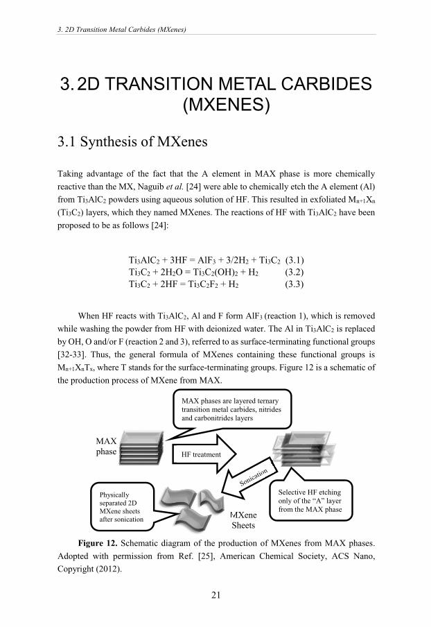
Taking advantage of the fact that the A element in MAX phase is more chemically
reactive than the MX, Naguib et al. [24] were able to chemically etch the A element (Al)
from Ti3AlC2 powders using aqueous solution of HF. This resulted in exfoliated Mn+1Xn
(Ti3C2) layers, which they named MXenes. The reactions of HF with Ti3AlC2 have been
proposed to be as follows [24]:
Ti3AlC2 + 3HF = AlF3 + 3/2H2 + Ti3C2 (3.1)Ti3C2 + 2H2O = Ti3C2(OH)2 + H2 (3.2)Ti3C2 + 2HF = Ti3C2F2 + H2 (3.3)
When HF reacts with Ti3AlC2, Al and F form AlF3 (reaction 1), which is removed
while washing the powder from HF with deionized water. The Al in Ti3AlC2 is replaced
by OH, O and/or F (reaction 2 and 3), referred to as surface-terminating functional groups
[32-33]. Thus, the general formula of MXenes containing these functional groups is
Mn+1XnTx, where T stands for the surface-terminating groups. Figure 12 is a schematic of
the production process of MXene from MAX.
Figure 12. Schematic diagram of the production of MXenes from MAX phases.
Adopted with permission from Ref. [25], American Chemical Society, ACS Nano,
Copyright (2012).
MAX
phase
MXene
Sheets
MXene
HF treatment
MAX phases are layered ternarytransition metal carbides, nitrides and carbonitrides layers
Physically separated 2D MXene sheets after sonication
Selective HF etching only of the “A” layer
from the MAX phase

3. 2D Transition Metal Carbides (MXenes)
22
3.1.1 Factors Influencing the Production of MXenes
Following the success in obtaining the first MXene, Ti3C2Tz, more MXene compounds
have been synthetized. Twenty-two MXene compounds, obtained from MAX phases and
MAX related phases, have been reported so far. They are: (Ti2CTz [25], Nb2CTz [23]
V2CTz [23], Mo2CTz (obtained from Mo2Ga2C) [31], (Ti0.5Nb0.5)2CTz [25], Mo1.33CTz
[39], W1.33CTz [37-38], Nb1.33CTz (presented in paper VI), Ti3CNTz [25], Ti3C2Tz [24],
Zr3C2Tz (obtained from Zr3Al3C5) [76], Hf3C2Tz (obtained from Hf3[Al(Si)]4C6) [77],
Ta4C3Tz [25], (V0.5Cr0.5)3C2Tz [25], Ti4N3Tz [27], Nb4C3Tz [78], V4C3Tz [79],
(Nb0.8Ti0.2)4C3Tz, (Nb0.8,Zr0.2)4C3Tz [80], Mo2TiC2Tz, and Mo2Ti2C3Tz, (where Mo and Ti
form an ordered layer structure, with Mo occupying the outer M layers, bonded to the
surface termination groups, and Ti occupying the inner M layers, similarly, in Cr2TiC2Tz,
the Cr occupies the outer layers [81]).
This list shows that MAX phases of different number of layers, n = 1, 2 and 3,
different M elements Ti, Nb, V, Mo, W, and Ta, different A elements, Al, Si [30] or Ga
[31], and different X elements C and/or N can be converted to MXenes. In addition, MAX
phases can contain two alloyed different M elements either ordered such as Mo and Ti or
randomly distributed such as V and Cr. Also, selectively etching one of the alloyed M
elements can create MXene with vacancies either randomly distributed, as with Nb1.33CTx
(paper VI), or ordered, such as Mo1.33CTz and W1.33CTz.
The process of synthesizing MXenes depends on many factors, such as the particle
size of the starting MAX phase powder, etching time, temperature, and HF concentration
[23]. Thus, tuning these factors leads to increased yields, reduced etching times and
improved quality of the produced MXenes. For example, reducing the particle size of
Ti3AlC2 from above 53 μm to less than 38 μm resulted in the decrease in the time needed
for its complete conversion to Ti3C2Tz in a 50 % HF solution from 19 h to only 2 h [82].
The same holds true for V2AlC: it was shown that decreasing the particle size by attrition
milling instead of using a titanium-nitride-coated milling bit led to the reduction of
etching time from 90 to 8 h [23].
Several other factors affect the etching procedures. These factors are related to the
chemistry and structure of the MAX phase. Among them is the effect of changing the M
element, as well as changing n. MAX phases of different M element possess different
M-Al binding energies which affect the etching conditions needed to convert them to their
MXenes. For example, conversion of Ti2AlC to Ti2CTz needs shorter etching times and
lower HF concentrations than those needed for converting Nb2AlC to Nb2CTz (Table 1).
This can be explained by comparing the binding energy of Ti-Al to that of Nb-Al in
Ti2AlC, and Nb2AlC, respectively. Ti-Al has a lower binding energy of 0.98 eV compared
to that for Nb-Al, (1.21 eV) and V-Al (1.09 eV) [83]. More interestingly, as n, increases,
the chemical stability of the MXenes increases. For example, Ti3C2Tz, etched in 50 wt.%

3. 2D Transition Metal Carbides (MXenes)
23
HF, has a yield of 100 % whereas, 10 wt.% of HF is sufficient to produce Ti2CTz of a 60
% yield [24-25]. In addition, the bond strength of both M-X and M-A plays an important
role in determining which MAX phases can be converted into MXene by selectively
etching the A layer and which MAX phases will simply fully dissolve in the etchant [84].
For a MAX phase to be converted into MXene the M-A bonds must be weaker than the
M-X bonds. For example, in Ti3AlC2 and Nb2AlC, both the Ti-Al and Nb-Al bonds are
weaker than the Ti-C and Nb-C bonds [84]. On the other hand, when the M-A and M-X
bonds are of comparable strength, the MAX phase can dissolve in the etchant or remain
as is. For example, in hypothetical Sc2AlC and Cr2AlC, the Sc-Al and Cr-Al bonds are of
comparable strengths to those for Sc-C and Cr-C [84]. Therefore, other approaches would
be needed to synthesize Sc2CTz or Cr2CTz. This rule can also be used to selectively etch
one of the M elements in a quaternary MAX phase forming either ordered or randomly
distributed vacancies in the produced MXene, such as in etching (Mo2/3Sc1/3)2AlC to form
Mo1.33CTz with ordered vacancies [37] or in etching (Nb2/3Sc1/3)2AlC to form Nb1.33CTz
with disordered vacancies as shown in paper VI.
Apart from HF, other etchants were used to selectively etch the A layers and produce
MXenes. Most of them comprised an acid and a source of fluoride ions, such as NH4HF2
(used in paper I), LiF + HCl (used in paper II), NaBF4 + HCl [85], molten baths of KF,
LiF and NaF in the case of Ti4AlN3 to produce Ti4N3Tz [27]. Whereas, for selectively
removing Si layers from Ti3SiC2 and producing Ti3C2Tz, a mixture of HF and an oxidant
such as H2O2, (NH4)2S2O8, HNO3, KMnO4, FeCl3 was used [30]. A fluorine-free synthesis
route has been reported to produce Ti3C2Tz by etching Ti3AlC2 using a hydrothermal
process containing a 27.5 M NaOH solution at 270 ⁰C [86].
3.2 Exfoliation, Intercalation and Delamination of
MXenes
Delamination trials for the exfoliated MXenes have been carried out to separate the
stacked multilayers, MLs, into single flakes. The first approach was to sonicate the
exfoliated MXenes in water, isopropanol or methanol. This process resulted in a low yield
of single flakes that had relatively small lateral sizes (< 1 µm) [25].
After the removal of the Al layers by HF alone, the bond between the MXene layers
becomes weaker. However, it is still not weak enough to be broken by sonication alone,
which is the reason behind the low yield of delaminated flakes after sonication. One
approach commonly used for obtaining 2D layers is intercalation of a compound between
the layers, which breaks the bonds between the layers and isolates the layers from each
other. This method was used decades ago to exfoliate vermiculite [87], as well as other
3. 2D Transition Metal Carbides (MXenes)
24
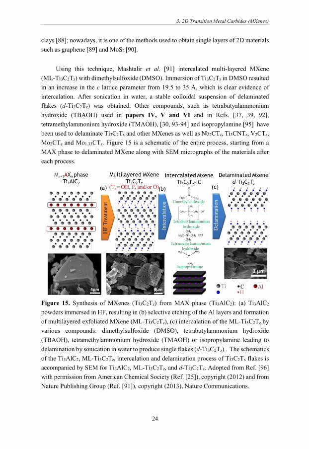
clays [88]; nowadays, it is one of the methods used to obtain single layers of 2D materials
such as graphene [89] and MoS2 [90].
Using this technique, Mashtalir et al. [91] intercalated multi-layered MXene
(ML-Ti3C2Tz) with dimethylsulfoxide (DMSO). Immersion of Ti3C2Tz in DMSO resulted
in an increase in the c lattice parameter from 19.5 to 35 Å, which is clear evidence of
intercalation. After sonication in water, a stable colloidal suspension of delaminated
flakes (d-Ti3C2Tz) was obtained. Other compounds, such as tetrabutyalammonium
hydroxide (TBAOH) used in papers IV, V and VI and in Refs. [37, 39, 92],
tetramethylammonium hydroxide (TMAOH), [30, 93-94] and isopropylamine [95] have
been used to delaminate Ti3C2Tx and other MXenes as well as Nb2CTz, Ti3CNTz, V2CTz,
Mo2CTz and Mo1.33CTz. Figure 15 is a schematic of the entire process, starting from a
MAX phase to delaminated MXene along with SEM micrographs of the materials after
each process.
Figure 15. Synthesis of MXenes (Ti3C2Tz) from MAX phase (Ti3AlC2): (a) Ti3AlC2
powders immersed in HF, resulting in (b) selective etching of the Al layers and formation
of multilayered exfoliated MXene (ML-Ti3C2Tz), (c) intercalation of the ML-Ti3C2Tz by
various compounds: dimethylsulfoxide (DMSO), tetrabutylammonium hydroxide
(TBAOH), tetramethylammonium hydroxide (TMAOH) or isopropylamine leading to
delamination by sonication in water to produce single flakes (d-Ti3C2Tz) . The schematics
of the Ti3AlC2, ML-Ti3C2Tz, intercalation and delamination process of Ti3C2Tx flakes is
accompanied by SEM for Ti3AlC2, ML-Ti3C2Tz, and d-Ti3C2Tz. Adopted from Ref. [96]
with permission from American Chemical Society (Ref. [25]), copyright (2012) and from
Nature Publishing Group (Ref. [91]), copyright (2013), Nature Communications.

3. 2D Transition Metal Carbides (MXenes)
25
The other approach is to combine etching, exfoliation and delamination in one step.
Ghidiu et al. [97] showed that immersing Ti3AlC2 in a solution of LiF + HCl, not only
etched the Al layers producing Ti3C2Tz, but also resulted in the MLs spontaneously
delaminating in water. The reason for the spontaneous delamination is that Li+ ions are
intercalated between the layers during etching. These ions are also accompanied by
hydration shells of H2O. The intercalation of both the Li+ ions and the water layers weaken
the bonding between the flakes sufficiently, facilitating the delamination process.
MXenes can be intercalated by other molecules, such as hydrazine, urea, along with
cations other than Li+, such as (Na+, K+, Rb+, Mg+2 and alkylammonium cations) [91, 98-
99]. Furthermore, the exchange of intercalant cations was reported for Ti3C2Tz [100],
where Li+ cations were first intercalated, then exchanged by K+, Rb+, Na+, Mg2+ or Ca2+.
3.3 Structure of MXenes The first proposed models for ML Ti3C2Tx were based on density functional theory,
(DFT), simulations [24]. In those models, all Tz were assumed to be either OH or F.
Simulated XRD diffraction patterns were obtained from these models and compared with
XRD diffraction patterns obtained experimentally for Ti3C2Tx as shown in Figure 13. The
Ti3C2(OH)2 is the closest to the experimental one; however, experimental results obtained
from XPS and NMR analysis show the presence of OH, O and F terminations [32-33].
The ratios of OH+O to F terminations can vary according to the concentration of HF used
in etching. For example, Ti3AlC2 etched using 50% HF would have an OH + O to F ratio
of 0.5:1.0, while using 10% HF increases the ratio to ≈ 1:1 [96].
Figure 13. XRD patterns for Ti3AlC2 before and after HF treatment, Ti3C2Tz after
sonication in water (exfoliated) and simulated XRD patterns of Ti3C2F2, Ti3C2(OH)2
structure models. Reprinted with permission from John Wiley and Sons, Advanced
Materials (Ref. [24]), copyright (2011).
3. 2D Transition Metal Carbides (MXenes)
26
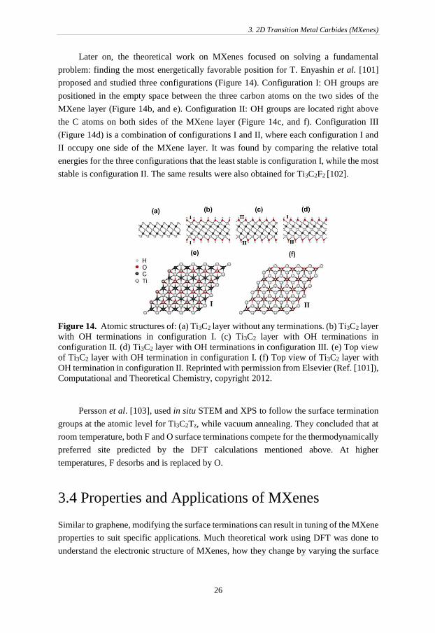
Later on, the theoretical work on MXenes focused on solving a fundamental
problem: finding the most energetically favorable position for T. Enyashin et al. [101]
proposed and studied three configurations (Figure 14). Configuration I: OH groups are
positioned in the empty space between the three carbon atoms on the two sides of the
MXene layer (Figure 14b, and e). Configuration II: OH groups are located right above
the C atoms on both sides of the MXene layer (Figure 14c, and f). Configuration III
(Figure 14d) is a combination of configurations I and II, where each configuration I and
II occupy one side of the MXene layer. It was found by comparing the relative total
energies for the three configurations that the least stable is configuration I, while the most
stable is configuration II. The same results were also obtained for Ti3C2F2 [102].
Figure 14. Atomic structures of: (a) Ti3C2 layer without any terminations. (b) Ti3C2 layer
with OH terminations in configuration I. (c) Ti3C2 layer with OH terminations in
configuration II. (d) Ti3C2 layer with OH terminations in configuration III. (e) Top view
of Ti3C2 layer with OH termination in configuration I. (f) Top view of Ti3C2 layer with
OH termination in configuration II. Reprinted with permission from Elsevier (Ref. [101]),
Computational and Theoretical Chemistry, copyright 2012.
Persson et al. [103], used in situ STEM and XPS to follow the surface termination
groups at the atomic level for Ti3C2Tz, while vacuum annealing. They concluded that at
room temperature, both F and O surface terminations compete for the thermodynamically
preferred site predicted by the DFT calculations mentioned above. At higher
temperatures, F desorbs and is replaced by O.
3.4 Properties and Applications of MXenes Similar to graphene, modifying the surface terminations can result in tuning of the MXene
properties to suit specific applications. Much theoretical work using DFT was done to
understand the electronic structure of MXenes, how they change by varying the surface

3. 2D Transition Metal Carbides (MXenes)
27
terminations and what the influence of that variation is on their properties [24, 102, 104-
108].
For example, DFT calculations predict that MXene monolayers without surface
terminations are metallic and that their electron density of states, DOS, near the Fermi
level, Ef, are higher than that of their parent MAX phases [24, 102, 104-105]. In MAX
phases, taking Ti2AlC as an example, the valence states below Ef are divided into two
sub-bands. One of them, which is the nearest to Ef, is mainly composed of a hybridization
between Ti 3d and Al 3p orbital; this sub-band is denoted sub-band A (Figure 16). The
other sub-band, denoted B, is located further away from Ef between -10 and -3 eV and is
formed from the hybridization between Ti 3d and C 2p orbitals. In MXenes, the removal
of the A element leads to the reformation of sub-band A due to the removal of Al 3p
orbitals. Thus sub-band A will be composed of only Ti 3d orbitals meaning that the nature
of the bonding becomes a metallic Ti-Ti bonding, resulting in the increase of DOS near
the Ef of Ti2C compared to Ti2AlC [106].
These findings can also influence the magnetic properties of MXenes. The increase
in the electron DOS near the Ef caused by the d orbitals of M could potentially lead to
magnetic properties [104-105, 109]. For example, DFT calculations predict that Cr2C,
Cr2N [105] and Ta3C2 [109] are ferromagnetic, while Ti3C2 and Ti3N2 [104] are
antiferromagnetic. Such magnetic properties disappear as soon as the MXenes are
terminated with any functional groups due to changes in the sub-band A from M-M
bonding to M-T bonding, causing a reduction in electron DOS near the Ef. That is not true
for Cr2C and Cr2N, where theoretical calculations show that Cr2CTz will stay magnetic
up to almost room temperature[105]. It is worth noting that so far, no one has reported
the production of Crn+1XnTz experimentally.
Surface terminations also influence whether a particular MXene compound is a
metal, semiconductor or insulator. Through theoretical calculations, the band gaps of bare
MXenes and MXenes with various surface terminations were predicted. As stated above,
bare MXenes surfaces are predicted to be metallic-like conductors, and most surface
terminated MXenes are metallic. However, some surface terminated MXenes vary from
being semiconductors with a small band gap to large direct or indirect band gap, as shown
in Table 1. The key to understanding the reason behind the changes in band gap is how
the electron DOS near Ef changes when MXenes are surface terminated, as shown in
Figure 16 [4,37,44,45]. The existence of the surface terminations results in the formation
of a third sub-band, sub-band C, located below sub-band B. The latter is formed due to
the M-T bonds moving the gap between sub-band A and B to lower energies.
.

3. 2D Transition Metal Carbides (MXenes)
28
Table 1. Band gap values calculated theoretically for various MXenes with different surface terminations.
*indirect band gap. **direct band gap
Figure 16. Partial density of states of Ti2AlC, and Ti2CTz, where Tz is O2, F2, H2 or(OH)2. Reprinted with permission from American Physical Society, Physical Review B (Ref. [106]), copyright (2013).
Most of the theoretical results obtained for different MXenes cannot be directly
implemented on the MXenes produced experimentally, due to the lack of a structure
model that takes into consideration the fact that the surface terminating groups, T, in
MXenes are not composed of one functional group, but more than one. Another problem
with the theoretical studies is that they only predict properties for isolated layers while
Compound Band gap, eV Ref.Ti3C2(OH)2 0.05 [24]Ti3C2(F)2 0.10 [24]Ti2CO2 1.03* [105]
Sc2C(OH)2 0.45** [105]Sc2C(F)2 1.80* [105]Sc2CO2 0.24* [105]Zr2CO2 0.88* [105]Hf2CO2 1.00* [105]

3. 2D Transition Metal Carbides (MXenes)
29
MXenes are experimentally produced in the form of MLs. Recently a few theoretical
researchers started to address these two issues. Among them is Caffrey [110], who
reported the predicted DOS of Ti3C2T2 and V2CT2 assuming mixed surface terminations
of –O, –OH and –F and also assuming MLs to reflect a typical experimental composition
and form. The DOS for multi-layered Ti3C2T2 was found to predominantly comprised the
contributions from the Ti and C atoms in the range from -4 to +2 eV. For V2CT2, the
contributions from V and C were found to dominate the energy region from -2 to +4 eV.
In both cases, the states associated with surface terminations were located at lower energy
regions (below -2 eV). It was predicted that Ti3C2(OH)2 has a low work function of about
2 eV, which would allow such material to be an efficient field emitter [111]. However,
that low work function increases drastically when the –OH is replaced with -F, -O or even
mixed with them where the percentage of –OH is less than 60% [110]. Similar DFT
calculations were performed for Mo2CT2 and Mo1.33CT2, where T is –O or –F (–OH
terminations were approximated with –F in this study) [112]. The electronic properties of
both MXenes were predicted to strongly depend on the O to F ratio. If the O to F ratio is
1:2 the electronic structure was predicted to be more metallic. If the O to F is 2:1, the
Fermi level is lowered to a non-metallic state. Mo2CTz shows a preference of –O
terminations to –F as compared to Mo1.33CTz which prefers -F to -O terminations. This
prediction is in agreement with the chemical composition of both MXenes obtained
experimentally from XPS. The DOS at Ef was predicted to be dominated mainly by the
Mo orbitals, while the orbitals of both O and F are located at lower energies, which is the
same case as for Ti3C2T2 and V2CT2 [110].
Similar to the MAX phases, MXenes of different elements and n layers vary in their
electrical resistivities [113]. The resistivity of cold pressed freestanding discs for different
exfoliated MXenes is about four times higher than that for their parent MAX phases. For
example, the resistivity of cold pressed Ti3AlC2 is 1200 μΩm, while that for Ti3C2Tz is
5000 μΩm [25]. The sheet resistance values reported for MXenes are comparable to those
for multilayered graphene [1, 114-115]. The etching time as well as intercalation of
various compounds in MXenes were found to play an important role in changing the
resistivities of cold pressed MXenes discs [82]. Increasing etching time of Ti3AlC2 results
in a significant increase in resistivity of the produced Ti3C2Tz [82]. Mashtalir et. al [34],
reported on the increase of resistivity of cold pressed discs of Ti3C2Tz, Ti3CNTz, Nb2CTz
and TiNbCTz after intercalation with hydrazine monohydrate. This behavior is similar to
other 2D materials, such as the intercalation of TaS2 with hydrazine [116]. MXenes have
also been reported to be hydrophilic based on measurements of the contact angle on cold
pressed discs. The hydrophobicity of the MXenes would be an advantage when using
MXenes in energy storage devices containing aqueous electrolytes or dispersing them in
water or alcohol.

3. 2D Transition Metal Carbides (MXenes)
30
The mechanical properties of MXenes have been of interest due to their strong
M-X bonds. Their elastic properties have been predicted by calculating the elastic
constant when stretched along the basal planes, c11, using DFT calculations [24, 117].
MXenes show high values of c11 compared to their parent MAX phases; however, these
values are lower than those reported for graphene [118]. Very recently, the elastic
properties of single and bilayers were reported [119]; the effective Young’s modulus for
a single flake of Ti3C2Tz obtained from a solution processed synthesis technique is 330 ±
30 GPa. This value is higher than that of other 2D materials such as graphene oxide,
reduced graphene oxide and MoS2, but lower than that of h-BN and graphene.
Energy storage applications are considered one of the early explored applications
for MXenes especially Li ion batteries (LIBs). Theoretical as well as experimental studies
show promising behavior for MXenes as anodes in LIBs [23, 102, 104, 120]. Theoretical
calculations predict that Ti3C2 could achieve a better performance as an anode in LIBs
compared to TiO2 because of its higher electrical conductivity stemming from its metallic
nature, its lower open circuit potential and its high charge/discharge rates [102]. Although
several MXenes (Ti3C2Tz [91], Ti2CTz [120], V2CTz [23] and Nb2CTz [23]) have been
experimentally studied for their performance as anodes in LIBs, the most exciting results
were obtained for delaminated Ti3C2Tz [91]. Delaminated Ti3C2Tz - used as anodes with
no additives - showed a reversible capacity 4 times higher than that of exfoliated Ti3C2Tz,
as shown in Figure 17. Furthermore, delaminated Ti3C2Tz free-standing thin film proved
to be capable of maintaining good capacity at high rates (110 mAhg-1 at 36 C after 700
cycles). Also in the field of energy storage, Ti3C2Tz rolled into film, produced by etching
Ti3AlC2 by LiF+HCl solution, shows a volumetric capacitance exceeding 900 F/cm3,
which is much higher than that of the porous carbon currently used in electrochemical
capacitors [97]. MXenes have also been shown to operate at charge rates exceeding those
of conventional electrical double-layer capacitors (EDLCs) and still provide higher
capacitance of ≈ 200 F/Cm3 at a scan rate of 10 V/s [121].
Figure 17. Performance of exfoliated and delaminated Ti3C2Tz as anodes in LIBs. Inset
shows the delaminated Ti3C2Tx free-standing thin film after filtration through the alumina
membrane, scale bar is 4 μm long. Reprinted with permission from Nature Publishing
Group (Ref. [91]), copyright (2013), Nature Communications.

3. 2D Transition Metal Carbides (MXenes)
31
Ti3C2Tz was also used as a supporting material for platinum nanoparticles [122].
The Ti3C2Tz/Pt catalysts showed extraordinary stability and durability compared to the
conventionally used Pt/C catalysts for proton exchange membrane fuel cells. MXenes
such as Mo2CTz, Mo1.33CTz, W1.33CTz, V4C3Tz showed promise as active catalyst
candidates for hydrogen evolution reactions [39, 79, 123]. Nb2CTx has been reported to
show promising performance for photothermal cell ablation and as a photocatalyst for
hydrogen evolution, besides the good performance for energy storage applications [23,
95, 124-125]. Furthermore, MXenes have shown promise in other applications, such as
transparent conducting electrodes (paper I), water treatment, electromagnetic shielding,
gas sensors and biosensors [126-132]. Using both DFT calculations and molecular
dynamics simulations, the hydrogen storage properties for Ti2C, Sc2C and V2C were
studied, showing the possibility of hydrogen storage up to about 3.4 wt.% reversibly at
room temperature [133]. In summary, one can say that MXene is a large family of 2D
materials with huge promise for many applications.


4. Electronic Transport Properties in Disordered Systems
33
4. ELECTRONIC TRANSPORT PROPERTIES IN DISORDERED
SYSTEMS
Disordered systems are materials which have a disorder in the arrangement of the atoms
in the crystal lattice. Disorder can arise from defects, such as atomic vacancies,
dislocations, alloying or intercalation. Such materials include ligand-stabilized
metal-cluster compounds (e.g. [FeCo3(CO)12]- anions [134] and Au55[P(C6H5)3]12Cl6
[135]), ceramic metals (cermets such as Ni-SiO2, Pt-SiO2134, Au-Al2O3 and
W-Al2O3) [136], various other metal-nonmetal composites [137], and doped or
amorphous semiconductors [138-139].
Disordered systems can be classified into three categories according to their
resistivity ratios (𝜌𝑟 =𝜌1.4 𝐾
𝜌300 𝐾): 1. Metallic regime: ρr < 2, critical regime: 2 < ρr < 6, and
3. insulating regime: ρr > 6 [140]. These three regimes can be better characterized by
plotting ln W vs. ln T, where W is defined as the reduced activation energy,
𝑊 = −𝑇𝑑(ln(𝜌))
𝑑(𝑙𝑛(𝑇)) [141]. For disordered systems in the metallic regime, W decreases with
decreasing T. In the critical regime, W is constant, with decreasing T. In the insulating
regime, W would increase with decreasing T. Figure 18 is an example, plotting W vs. T
for polyaniline doped with camphor sulfonic acid. These materials exhibit the three
regimes depending on the degree of disorder arising from the doping.
Figure 18. Log-log plot of W vs. temperature for polyaniline doped with camphor
sulfonic acid materials in the metallic, critical and insulting regimes. Reprinted with
permission from American Physical Society, Physical Review B (Ref. [140]), copyright
(1993).

4. Electronic Transport Properties in Disordered Systems
34
4.1 Conduction mechanisms in disordered systems
In metals, the conductivity as a function of temperature is described by the scattering of
Bloch waves by impurities and defects, which leads to a Boltzmann transport equation
[142] written as:
𝜎(𝑇) = 𝜎0 − 𝐴 𝜎02𝑇𝑛 (4.1)
where 𝜎0 is the residual conductivity due to impurity and defect scattering,
𝐴 is a positive constant
𝑛 is a positive integer > 2 (n = 2 if the electron-electron interactions are dominant).
The residual conductivity 𝜎0 increases as T increases due to the increase of the
amount of scattering as the excitation of phonons or electron-electron interactions
collision increases. However, this equation does not hold if the disorder is strong.
The coefficient 𝐴 can then be positive or negative, and 𝑛 is ½ for three-dimensional
systems [142]. Thus, several theoretical models have been proposed to describe the
conduction mechanism in disordered systems. These models address two problems:
(1) Dealing with the nature of the wave function of a single electron in the presence of a
random potential (Anderson localization) and, (2) The interaction among electrons in the
presence of a random potential. A Hamiltonian describing the conductivity of a strongly
correlated electron system in interaction with the underlying lattice, would contain the
following terms [137]:
ℋ = ℋe + ℋph + ℋe-e + ℋe-ph + ℋv (4.2)
The first term describes the non-interacting electron system using a tight binding
model, the second is the phonon term, the third is the electron-electron interactions, the
fourth is the electron-phonon interaction and the last term is for the potential seen by the
electrons as they move through the lattice. The variable-range hopping models discussed
later make an approximation of the Hamiltonian, which is called the single-electron
approximation where the ℋe-e is ignored. However, models based on the work of
Hubbard, Mott and Anderson consider the electron-electron interaction, ℋe-e, but consider
a rigid lattice.

4. Electronic Transport Properties in Disordered Systems
35
4.1.1. Hubbard-Anderson Hamiltonian
Before describing the Hubbard-Anderson Hamiltonian, the two terms “Anderson
localization” and “mobility edge” have to be defined first. The traditional view of how
disorder affects crystalline systems was that the random potential would cause the Block
waves to lose phase on the length scale of the mean free path l. However, the wave would
remain extended throughout the sample. Anderson showed that this is not true and the
wave function in a random potential may be altered if the randomness or disorder is strong
enough [143]. This means that if the disorder is very strong, the wave function may
become localized, in that the envelope of the wave function decays exponentially from
some point in space. A comparison between the traditional view of the wave function and
Anderson localization is demonstrated in Figure 19. Localization can take place due to
electron-electron interaction, disorder or electron-phonon interactions.
Figure 19. Wave functions (a) extended throughout the sample with mean free path l;
(b) localized with localization length ξ. Reprinted with permission from American
Physical Society, Reviews of Modern Physics (Ref. [137]).
The mobility edge is defined as the amount of energy required to change the
character of the states from being localized to being extended [144]. If the Fermi level
lies in the region of localized states, the conductivity at 0 K would be zero and the
conductivity at the extended states would have a value at 0 K. Therefore, the mobility
edge separates metals from insulators.
Anderson-Hubbard Hamiltonian describes the interactions- or disorder-induced
localization as follows [137].:
ℋ = ∑ 𝜀𝑚 𝑛𝑚,𝜎 + ∑ 𝐽𝑚′,𝑚 𝑎𝑚′𝜎+ 𝑎𝑚,𝜎 + 𝑈 ∑ 𝑛𝑚↑ 𝑛𝑚↓𝑚𝑚 ≠𝑚′,𝜎𝑚,𝜎 (4.3)
where 𝜀 is the energy of site 𝑚
𝐽𝑚′,𝑚 is the transfer integral between sites 𝑚′ and 𝑚,
𝑈 is the Hubbard on-site correlation energy,
𝑎𝑚,𝜎+ 𝑎𝑚,𝜎 are quantum-mechanical operators that respectively create and
annihilate an electron at site 𝑚 with spin 𝜎, and
𝑛𝑚𝜎 is the number of electrons at site 𝑚 with spin 𝜎.

4. Electronic Transport Properties in Disordered Systems
36
The second term in Eq. (4.3) is the first term in Eq. (4.2), describing a tight-binding
band of electrons. The third term, introduced by Hubbard, is to take into account the
(on-site) interactions between electrons. However, in the Hubbard model, all sites were
assumed to have the same energy, therefore, 𝜀 would be constant and the first term in Eq.
(4.3) can be discarded. In this case, the ratio between 𝑈 and 𝐽𝑚′,𝑚 would be the only factor
driving the metal-nonmetal transition. If 𝑈 ≫ 𝐽𝑚′,𝑚 the charges would be localized,
while if 𝐽𝑚′,𝑚 ≪ 𝑈 the charges would be delocalized into a band, i.e. extended states
would form. If we consider the case where the electron-electron interactions on-site were
discarded, i.e. 𝑈 = 0, 𝐽𝑚′,𝑚 = 𝐽0 and 𝜀𝑚 is distributed randomly over a certain range
with a width of Γ around zero [143]. In such a case, if Γ = 0, then all the states are
extended; if Γ > 0, the electronic states become localized if Γ/z𝐽0 (where z is the number
of nearest neighbors) reaches a critical value. This critical value is called the Anderson
transition. In general, the states near a band edge are the easiest to localize, i.e., do not
need a large disorder to be localized. However, if the disorder is high enough, the
valence- and conduction-band tails of a semiconductor may overlap to give a nonzero
density of localized states, which originally would have been the energy gap if there were
no disorder (semiconductor single band).
It is worth noting that, in the Hubbard-Anderson approach, a rigid lattice is
considered. This means that polaronic deformations around the moving charge are not
taken into account and quantum mechanical tunneling is the only mechanism of charge
transfer between neighboring sites. However, by introducing the phonon contribution,
other transport mechanisms can be considered, such as thermally activated hopping at
least at sufficiently high temperatures. This has been demonstrated in paper V, where the
conduction mechanism for Mo-based MXenes changes from variable range hopping
mechanisms at low temperature to a thermally activated mechanism at higher
temperatures.
4.1.2. Weak localization in thin films and 2D materials
Thin disordered metal films show a deviation from the Boltzmann theory, where at
low temperatures the resistivity increases with decreasing temperature. In addition, such
thin films experience a decrease in resistivity when magnetic fields perpendicular to the
films are applied, i.e. negative magnetoresistance (MR), and the resistance is strongly
dependent on the temperature. The value of the negative MR increases with decreasing
temperature. An example is a copper thin film with a thickness of 80 Å and a high degree
of disorder where its electronic mean free path is of the order of 10 Å [145].
Due to the occurrence of defects and/or impurities, the conduction electrons can be
scattered without losing their phase coherence, which would result in multiple scattered
waves forming a chaotic pattern. The usual Boltzmann theory neglects the interferences

4. Electronic Transport Properties in Disordered Systems
37
between the scattered waves and assumes that the momentum of the electron wave
disappears after the time τ0, inelastic lifetime of the electron in an eigenstate of
momentum (or τtr, transport mean free path). In this case, τ0 is assumed to be equal to τtr.
This assumption leads to the Drude formula for the conductivity of free electrons [145]:
𝜎 =𝑛𝑒2
𝑚𝜏𝑜 (4.4)
where 𝑛 is the number of electrons, and
𝑚 is the mass of an electron.
A correction has to be introduced to account for the interference between the
scattered spatial wave. That correction was shown to be [146]:
Δ𝐿 = −Δ𝑅
𝑅02 = 𝐿00log (𝜏𝑖/𝜏0); 𝐿00 = 𝑒2/(2𝜋2ℏ) (4.5)
where 𝑅 is the resistance, and
𝜏𝑖 is the inelastic lifetime, which is the lifetime in an eigenstate of energy.
This correction is temperature-dependent because the inelastic lifetime depends on
temperature. Thus, weak localization can be experimentally determined if plotting
resistance, R, vs. log T gives a straight line.
A thin film is considered 2D with respect to weak localization when the diffusion
time across its thickness is compared to the characteristic time of the electrons. In the
absence of a magnetic field this time is the inelastic lifetime of the conduction electrons
[145].
The MR behavior is an important characteristic that helps to differentiate weak
localization phenomenon from other conduction mechanisms, such as Coulomb
interactions, in disordered materials. The latter also have a linear relationship of resistance
with log T, as seen from its conductance correction [145]:
Δ𝐿(𝑇) = −Δ𝑅
𝑅02 = −𝐿00(1 − 𝐹)ln (𝑇) (4.6)
where F is the screening factor.
The mechanism of Coulomb interaction arises from the fact that the
electron-electron interaction in disordered metals is retarded, in other words, a sudden
change of the charge distribution in the disordered metal, which cannot be screened
immediately. Electrons in this case move by diffusion; thus, they will need time to screen
the charge distribution. As indicated above, in the case of weak localization, the MR
becomes negative and larger at lower temperatures. This is attributed to the effect of the
magnetic field on the quantum interference between forward-scattering events. Both weak
localization and Coulomb interaction can simultaneously take place. For example, in
Bi-films, they can be separated by applying a high magnetic field, which suppresses the
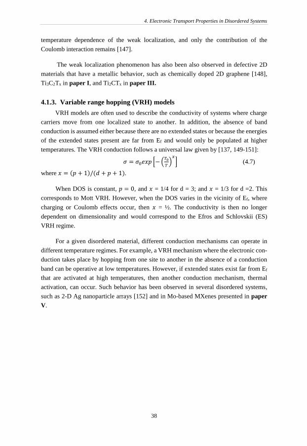
4. Electronic Transport Properties in Disordered Systems
38
temperature dependence of the weak localization, and only the contribution of the
Coulomb interaction remains [147].
The weak localization phenomenon has also been also observed in defective 2D
materials that have a metallic behavior, such as chemically doped 2D graphene [148],
Ti3C2Tx in paper I, and Ti2CTx in paper III.
4.1.3. Variable range hopping (VRH) models
VRH models are often used to describe the conductivity of systems where charge
carriers move from one localized state to another. In addition, the absence of band
conduction is assumed either because there are no extended states or because the energies
of the extended states present are far from Ef and would only be populated at higher
temperatures. The VRH conduction follows a universal law given by [137, 149-151]:
𝜎 = 𝜎0𝑒𝑥𝑝 [−(𝑇0
𝑇)𝑥
] (4.7)
where 𝑥 = (𝑝 + 1)/(𝑑 + 𝑝 + 1).
When DOS is constant, 𝑝 = 0, and 𝑥 = 1/4 for d = 3; and 𝑥 = 1/3 for d =2. This
corresponds to Mott VRH. However, when the DOS varies in the vicinity of Ef, where
charging or Coulomb effects occur, then 𝑥 = ½. The conductivity is then no longer
dependent on dimensionality and would correspond to the Efros and Schlovskii (ES)
VRH regime.
For a given disordered material, different conduction mechanisms can operate in
different temperature regimes. For example, a VRH mechanism where the electronic con-
duction takes place by hopping from one site to another in the absence of a conduction
band can be operative at low temperatures. However, if extended states exist far from Ef
that are activated at high temperatures, then another conduction mechanism, thermal
activation, can occur. Such behavior has been observed in several disordered systems,
such as 2-D Ag nanoparticle arrays [152] and in Mo-based MXenes presented in paper
V.

5. Characterization Techniques
39
5. CHARACTERIZATION TECHNIQUES
This chapter describes the most important techniques used in characterizing our
MXenes.
5.1 X-ray Diffraction (XRD)
X-ray diffraction (XRD) is one of the most common techniques used to characterize the
structure of materials, whether in powder, bulk or thin films forms. It is a non-destructive
technique, and it does not require extensive sample preparation. The technique is based
on the scattering of X-rays by atoms. Constructive interference is achieved at certain
angles governed by Bragg’s law [153]:
nλ = 2dsin θ (5.1)
where n is an integer,
λ is the wavelength of the probing rays,
θ is the angle between the incident rays and the surface of the crystal, and
d is the spacing between layers of atoms.
Constructive interference gives peaks at characteristic positions in X-ray
diffractograms, from which the lattice parameters, LPs, as well as phase identification, is
possible using a mode called θ/2θ scan. Here, θ is the angle between the incident beam
and the sample, and 2θ is twice that angle.
The θ/2θ scans in this thesis were performed for phase identification, as well as for
measuring the LPs. The scans were used to determine the conversion of MAX to MXene,
as well as whether intercalation of the produced thin MXenes films occurred (see paper
I). As shown in Figure 20, the (002) peak for a Ti3AlC2 thin film etched by HF is shifted
to lower 2θ values compared to the film before etching. This is due to the removal of the
Al layers, as well as the exfoliation of the films, resulting in an increase in the c-lattice
parameter from 18.6 to 19.8 Å. The film etched by NH4HF2, Ti3C2Tz-IC, (IC stands for
intercalated compound), is shifted further to the left compared to the Ti3AlC2 thin film
etched by HF. This shift is attributed to an increase in the c-lattice parameter to 24.7 Å,
indicating that intercalation took place when etching the thin film using NH4HF2.

5. Characterization Techniques
40
Figure 20. XRD patterns for thin films of Ti3AlC2, Ti3C2Tz and Ti3C2Tx-IC.
5.2 X-ray Reflectivity (XRR) X-ray reflectivity (XRR) is another non-destructive technique that is used to measure the
thickness, roughness, and density of thin films [153]. XRR uses the same θ/2θ
configuration as for phase identification but is performed using parallel beams where
beam divergence does not exceed 0.05° compared to the wide angle beam used for phase
identification. Moreover, the θ angle for XRR is much smaller (0 to 10°) compared to
what is usually used for θ/2θ scans. However, XRR has several limitations, including the
inability to measure film thickness beyond 300 nm. Thickness also cannot be measured
for thin films with roughness exceeding 50 nm. The technique itself does not work if there
is no difference in electron density between thin film and substrate.
Because XRR is more concerned with the refracted beam, Bragg’s law requires
modification as follows:
𝑚𝜆 = 2𝑑 𝑠𝑖𝑛𝜃√1 +2−1
sin𝜃2 (5.2)
where m is an integer number representing the order of Kiessig fringe (Figure 19), λ is the wave length of the probing rays, d is the film thickness, θ is the angle at which m is, and n is the refractive index. The thickness can be deduced from plotting sin2 θ vs. m2 and obtaining the slope, then
substituting in the following equation:
𝑑 = 𝜆
2√𝑠𝑙𝑜𝑝𝑒 (5.3)
6 8 10 12
Log.
Inten
sity (
arb.u
nits)
2 (
)
Ti3AlC2
Ti3C2Tx
Ti3C2Tx-IC

5. Characterization Techniques
41
10
100
1000
104
105
106
107
0 1 2 3 4 5 6
Inte
nsity
(log
)
Grazing incidence angle, 2theta (deg.) Figure 21. Typical XRR measurements for Ti3AlC2 thin film sputter-deposited for 10 min, resulting in a thickness of 28 nm.
Figure 21, shows an example of the XRR measurements for a 28 nm thick Ti3AlC2 thin film deposited on a sapphire substrate.
5.3 X-ray Photoelectron Spectroscopy (XPS) XPS is a surface sensitive technique used for compositional and chemical state analysis
of material surfaces [154]. The basic principle of XPS is the knocking out of electrons
from the core level of atoms via photons as shown in Figure 22. The electrons that manage
to reach the detector without energy loss result in photoelectron peaks that represent their
binding energy (BE). Each element in each specific chemical state has a characteristic
binding energy, which is determined from the measured kinetic energy (KE) by the
following equation [154]:
BE = hν – KE – Φ (5.4)
where hν is the energy of the x-ray photon,
Φ is the work function of the spectrometer.
Since the electrons that preserve their energy are the only ones that contribute to the
XPS spectrum as peaks, these electrons can only be ejected from the surface of the
sample; any electrons that are buried deep in the material would suffer from inelastic
m=1
m=2
m=3
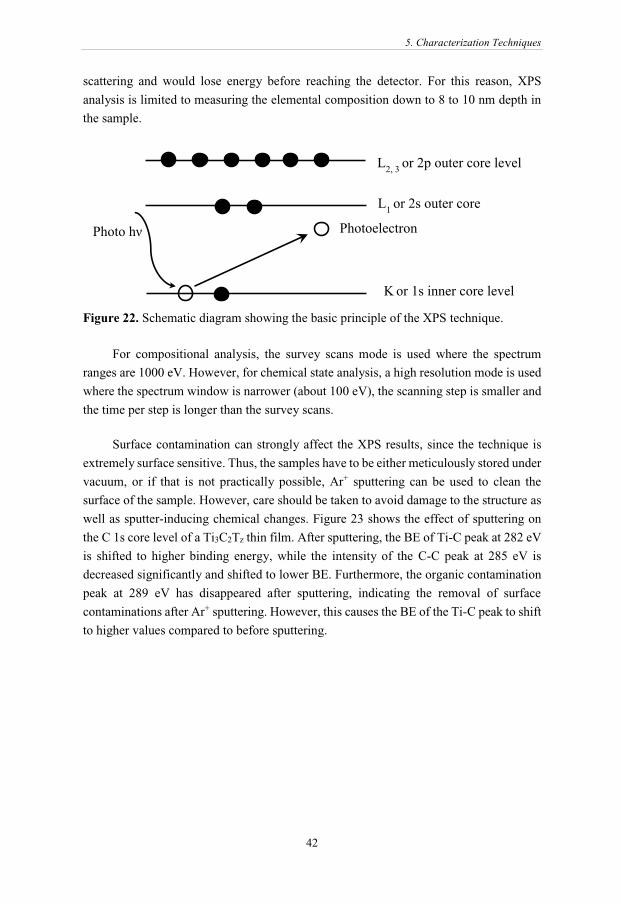
5. Characterization Techniques
42
scattering and would lose energy before reaching the detector. For this reason, XPS
analysis is limited to measuring the elemental composition down to 8 to 10 nm depth in
the sample.
Figure 22. Schematic diagram showing the basic principle of the XPS technique.
For compositional analysis, the survey scans mode is used where the spectrum
ranges are 1000 eV. However, for chemical state analysis, a high resolution mode is used
where the spectrum window is narrower (about 100 eV), the scanning step is smaller and
the time per step is longer than the survey scans.
Surface contamination can strongly affect the XPS results, since the technique is
extremely surface sensitive. Thus, the samples have to be either meticulously stored under
vacuum, or if that is not practically possible, Ar+ sputtering can be used to clean the
surface of the sample. However, care should be taken to avoid damage to the structure as
well as sputter-inducing chemical changes. Figure 23 shows the effect of sputtering on
the C 1s core level of a Ti3C2Tz thin film. After sputtering, the BE of Ti-C peak at 282 eV
is shifted to higher binding energy, while the intensity of the C-C peak at 285 eV is
decreased significantly and shifted to lower BE. Furthermore, the organic contamination
peak at 289 eV has disappeared after sputtering, indicating the removal of surface
contaminations after Ar+ sputtering. However, this causes the BE of the Ti-C peak to shift
to higher values compared to before sputtering.
Photo hν Photoelectron
L2, 3
or 2p outer core level
L1 or 2s outer core
level
K or 1s inner core level

5. Characterization Techniques
43
280285290295
Before Ar sputteringAfter Ar sputtering
Co
un
ts/s
Binding energy (eV) Figure 23. High resolution XPS spectra for C 1s core level before and after
sputtering for a Ti3C2Tz thin film.
Besides obtaining information from the core level of the atoms, XPS can be used to
determine the density of states (DOS) of the valence band. As expected, valence electrons
have lower BE than core level electrons, as they are positioned further from the nucleus.
Thus, the photoemissions from the valence electrons are located very close to the Fermi
level since the valence band is usually at a BE in the range of 0 to 15 or even 25 eV.
In order to properly identify the chemical species of an element based upon on XPS
spectra, calibration is essential. Such calibration can be done by calibrating with respect
to the BE of a certain element, the most common is adventitious C [154]. However, this
method is not accurate when Ar+ sputtering is performed, as this species is removed
and/or altered due to sputtering effects. The best method in that case, as in Papers I, III,
IV, and VI, is to calibrate the XPS spectra with respect to the zero eV Fermi level.
In papers I, III, IV, and VI, XPS was used for compositional analysis, as well as
for identification of chemical species through peak fitting of the high resolution spectra
and obtaining the chemical formulae of MXenes including the surface termination groups.
More details regarding the XPS peak fitting, analysis and calculations of the
amounts of surface terminations can be found in Refs. [32, 96].
5.4 Electron Microscopy Electron microscopes use electrons, which have shorter wavelengths than visible light
used in optical microscopy, as a probe. The main reason for using a source with shorter
wavelength is to increase resolution and magnification, achieving a resolution of
about 1 Å.

5. Characterization Techniques
44
A Transmission Electron Microscope (TEM) [155] depends on the transmission of
an electron beam through a sample for imaging and acquiring microstructural
information. Lattice imaging can be obtained using high-resolution TEM (HRTEM),
which is useful for studying the crystal structure and defects at an atomic level. For the
electron beam to be transmitted through the sample, the sample has to be quite thin, with
thicknesses below 100 nm. TEM and HRTEM were used in papers I, III, IV, and VI for
microstructure investigation and atomic resolution imaging.
More information regarding the crystal structure and grain orientation can also be
gathered by acquiring selected-area electron diffraction (SAED). SAED was used in
papers I, III, and VI for obtaining the LPs of the crystalline regions and identifying if
certain regions are crystalline or amorphous.
A scanning transmission electron microscope (STEM) focuses the electron beam
into a narrow spot, which is rastered over the sample and the transmitted electrons form
the image. Using both modes, the scanning and transmitting of electrons, it is possible to
acquire atomic imaging. This technique was used in paper I to image the atomic structure
of Ti3C2Tz thin films. With Electron Dispersive X-ray Spectroscopy (EDS), elemental
mapping can be acquired in STEM and TEM.
5.5 Ultraviolet-Visible Spectroscopy Ultraviolet-Visible Spectroscopy (UV-Vis) [156] measures the absorption of light in the
visible and ultraviolet ranges by a sample. It measures the intensity of light, I, at a given
wavelength after passing through the sample and compares it to the intensity of the
original beam (Iₒ). The ratio I/Iₒ is called the transmittance and is usually expressed as
percentage (%T). Absorbance is the negative log of transmittance and is related through
the Beer-Lamber-Bouguer Law. UV-Vis was used in paper III to obtain the
transmittance for MAX and MXene thin films.
5.6 Electrical Characterization
5.6.1 Four-point probe
The four-point probe technique is usually used for measuring the electrical resistivity of
thin films [157]. This technique consists of four equidistant probes that come in contact
with the surface of the film, as shown in Figure 24. The current is applied through the
outer two probes while the voltage between the two inner probes is measured. The value
obtained is the sheet resistance (Rs), which is the resistivity (ρ) divided by the thickness
of the film (t) and multiplied by a geometrical factor to account for the geometry of the

5. Characterization Techniques
45
sample measured. This technique was used to measure the resistivity of the MAX and
MXene thin films in paper III.
Figure 24. Schematic demonstrating the setup of the four-point probe technique.
5.6.1 Physical Properties Measurement System (PPMS)
PPMS is a system for measuring magneto-transport properties, such as:
(1) temperature- dependent resistivity, . The is measured as a function of temperature
which in turn can be used to shed light on the electronic transport in materials. (2) Hall
effect: When a magnetic field, B, is applied perpendicular to an applied current in a
conductor, a potential difference (RH), which is perpendicular to both the applied current
and B, is created as a result of the deflection of charge carriers due to their interaction
with B. In a single band model, the number of charge carriers and their mobility can be
obtained from measuring the and RH, since in this case the following equations can be
used:
𝜌 = 1
𝜎= 𝑒([𝑛 𝑜𝑟 𝑝]𝜇) (5.5)
𝑅𝐻 =1
𝑒𝑛(5.6)
where n is the number of electrons per unit volume,
p is the number of holes per unit volume, and
µ is the mobility of such charge carrier.
t
V
S3S2S1
II

5. Characterization Techniques
46
mechanisms such as weak localization, where the resistivity decreases with the
application of a magnetic field, as in papers I and III.
5.7 Electrochemical Characterization Electrochemical characterizations are used to evaluate the performance of materials for
several applications such as batteries, supercapacitors, electrolysis (hydrogen evolution
reaction and oxygen evolution reaction) and corrosion resistance. In paper IV,
electrochemical characterization was used to evaluate the performance of Mo2CTz as
electrodes for both Li-ion batteries and supercapacitors. In this section, I will focus on the
characterization for these two applications.
5.7.1 Li-ion Batteries
The electrochemical characterization of a given material for Li-ion batteries is usually
done by evaluating the behavior of such material as an electrode. In paper IV, the
working electrode was a freestanding composite film of Mo2CTz and carbon nanotubes
(CNTs). Stainless steel coin cells were assembled inside an Ar-filled glovebox. Li foil
was used as a counter electrode. A separator of borosilicate glass fiber paper was used to
prevent electrical shorting. The electrolyte used was 1.2 M LiPF6 in ethylene carbonate
and dimethyl carbonate (in a mass ratio of 1:2, respectively).
Cyclic voltammetry (CV) was used to evaluate the performance of the working
electrode as a Li-ion battery electrode, where the voltage is varied from a 3 V to 5 mV at
a given scanning rate, and the current is recorded. The electrodes are cycled several times
between these two values to show the stability of the material. In addition to the CV
measurements, galvanostatic cycling was also performed, where a constant current is
applied through the cell and the voltage is recorded. This test helps to evaluate the charge
and discharge rates. From both the CV and galvanostatic tests, the Coulombic efficiency
and specific currents, a measure for the amount of charge can be plotted against the
number of cycles from which the stability of the electrode can be assessed.
5.7.2 Supercapacitors
In batteries, the energy is produced via a chemical reaction that releases electrical current.
The charge and discharge of batteries is slow, so they are efficient for storage of energy
for long times and its slow release. However, in supercapacitors, the energy is stored
electrostatically on the surface of the materials and usually does not involve chemical
reactions. They can be charged and discharged quickly relative to batteries, thus having
high power densities, and can last for significantly more cycles. However, the amount of
charge that can be stored per unit mass is much smaller compared to Li-ion batteries. A
three-electrode cell was used to characterize the electrochemical performance of Mo2CTz

5. Characterization Techniques
47
freestanding thin films as supercapacitor electrodes. The counter electrode used was
activated carbon; the reference electrode was Ag/AgCl; the active electrode was a
Mo2CTz freestanding thin film; the electrolyte used was 1M H2SO4. As with Li-ion
battery testing, CV and galvanostatic measurements were performed to evaluate the
materials’ performance, stability after a large number of charge/discharge cycles and the
capacitance at different scan rates.


6. Summary and Contribution to the Field
49
6. SUMMARY AND CONTRIBUTION TO THE FIELD
The aim of this thesis was to synthesize MXenes in forms that allow for the
characterization of their electronic transport properties. The MXenes presented in this
thesis have one of three forms: (1) Epitaxial thin films on sapphire substrate of Ti3C2Tz
(paper I) and Ti2CTz (paper III), (2) Single flakes of Ti3C2Tz on SiO2 (paper II), (3)
Delaminated freestanding films of Mo2CTz (paper IV and V), Mo1.33CTz, Mo2TiC2Tz,
Mo2T2C3Tz (paper V) and Nb1.33CTz (paper VI). Through electronic transport
characterization, I was able to study the effect of various parameters, such as the number
of MXene layers (thin film vs. single flake), stoichiometry (Ti2CTz vs. Nb2CTz), M
element composition (Ti-, Nb- and Mo-based MXenes) and vacancies (Nb1.33CTz). It is
worth noting that before the start of this work, there were no experimental studies
published on thin film MXenes or the electronic transport properties of MXenes.
The first step of my study was to synthesize the most common and widely
researched MXene, Ti3C2Tz, in thin film form and measure its transport properties. This
was done in paper I, where epitaxial Ti3C2Tx thin films were produced from etching
magnetron sputter deposited epitaxial Ti3AlC2 thin films on sapphire substrates using two
different etchants, HF and NH4HF2. The Ti3C2Tz films produced by NH4HF2 etching
showed an increase of about 25% in the c lattice parameter compared to their counterparts
that were produced by HF etching. According to the XPS analysis, this significant
increase is due to the intercalation of NH4+ and NH3 species.
Looking at the electronic transport properties, the Ti3C2Tz epitaxial thin films were
found to be metallic-like conductors at room temperature and down to 100 K, as the
decreases with decreasing temperature. Below that temperature, the films’ increases
with decreasing temperature. This behavior is due to weak localization, which is
characteristic of defective 2D materials. MR measurements show a decrease in of such
films with increasing magnetic field, again due to weak localization. The films show high
transparency - 90% - in the visible-to-infrared range for films of 19 nm thick etched by
NH4HF2. These Ti3C2Tz thin films demonstrated the possibility of using them as
transparent conductive electrodes.
To answer the fundamental question of whether MXenes are inherently 2D
materials or if their electronic properties are thickness-dependent required the synthesis
and isolation of single flakes of Ti3C2Tz and measuring their transport properties and

6. Summary and Contribution to the Field
50
comparing them with those of ML Ti3C2Tz thin films previously mentioned. In order for
the electronic transport properties for a single flake to be measured, it must have a lateral
size of more than 10 µm. The average flake size produced using either HF etching
followed by DMSO intercalation or with LiF+HCl was about 1 to 2 µm. In order to
increase the flake size to the desired dimensions, I started by increasing the grain size of
the precursor Ti3AlC2 phase from about 30 µm to about 70 µm by changing the synthesis
method from pressureless sintering to HIP. In the former, it is not possible to increase the
grain size by increasing the heating time, as TiC would start to precipitate at the grain
boundaries and, in turn, suppress grain growth. However, using HIP, the precipitation of
TiC was suppressed, and grain coarsening occurred. By etching the HIP-produced
Ti3AlC2 using LiF+HCl, MLs of lateral sizes ≈ 20 µm were produced. The MLs were
manually shaken in water to obtain single flakes through delamination. This resulted in
flakes with lateral dimensions of > 10 µm, as shown in paper II. It is worth noting that
the etching procedure was modified from the original reported in Ref. [97] by washing
the etched solution with 1 M HCl followed by 1 M LiCl, solution to remove remaining
LiF.
The transport measurements of the single flakes showed them to be metallic with a
room temperature of 10 µΩm. The density of free carriers was calculated to be about
8 x 1021 cm-3, while their mobility was estimated to be 0.7 cm2/Vs. The resistivity of the
single Ti3C2Tz flakes appeared to be five times higher than that of a 75 nm thick Ti3C2Tz
film, which showed the lowest value among all Ti3C2Tz thin films measured in paper
I. However, in later reports, the of Ti3C2Tz single flake was found to be about 2.2 µΩm,
a value similar to that of the best Ti3C2Tz thin films [158]. The same study reported an
increase in when the single flakes were subjected to oxygen or air with relative humidity
of 50%. This would explain the high value for the single flake in paper II. Because the
flakes were deposited from a colloidal aqueous suspension, if some adsorbate molecules
of oxygen or water did not desorb while vacuum annealing, this would lead to an increase
in .
The effect of the stoichiometry of MXenes on the electronic transport properties is
manifested in the comparison of the transport properties between Ti3C2Tz (paper I) and
Ti2CTz (paper III). The latter follows the same behavior as Ti3C2Tz thin films, i.e.
metallic behavior from RT down to about 40 K, followed by weak localization from 40
K to 10 K. The RT increases twofold when the stoichiometry, or n, is reduced from 2
to 1 for the same film thickness - for Ti3C2Tz it is 2.3 µΩm and for Ti2CTz it is 4.4 µΩm.
This increase in is most likely due to the absence of a Ti-C core; Ti3C2Tz has an extra
Ti layer in the center of the Ti-C blocks that is not bonded to surface terminations.
However, in Ti2CTz, all Ti layers are bonded to surface terminations. Since the surface
termination groups (-O, -OH, and/or -F) are mostly electron acceptors, it is not too

6. Summary and Contribution to the Field
51
surprising that Ti2CTz is more resistive. Thus, while decreasing n for Tin+1CnTz increased
, it did not alter the electronic transport mechanism.
In contradistinction, changing the transition metal M, from Ti in Ti2CTz to Nb in
Nb2CTz epitaxial thin films (paper III) and to Mo in Mo2CTz in delaminated
free-standing thin films (paper IV), obtained from vacuum filtration of a colloidal
suspension resulted in a change in transport mechanism. The resistivity-dependent
temperature measurements for Nb2CTz and Mo2CTz show an increase in resistivity with
decreasing temperature from RT to about 20 K. This behavior was found to be more
consistent with variable range hopping (VRH) models. The reason for the different
transport behavior of Ti2CTz compared to Nb2CTz and Mo2CTz might be due to the
interaction between the M metal and the surface termination groups, in addition to
disorder from the increase in the interlayer distance due to water or cation intercalation.
However, the exact reason is not understood at the moment.
The VRH mechanisms evaluated for Mo2CTz (paper IV) were shown to take place
at temperatures below 100 K. However, the transport mechanism from 100 K to RT was
not clearly understood. Therefore, paper V was dedicated to understanding the transport
mechanism more thoroughly for Mo-based MXenes. This included four compounds:
Mo2Ti2C3Tz, Mo2TiC2Tz, Mo2CTz, and Mo1.333CTz (the latter with ordered vacancies).
The compounds studied were in the form of delaminated free-standing thin films. From
the vs. T measurements, several points were evident: (1) for all samples, increased
with decreasing temperature, (2) Mo2CTz, before annealing, was the least conductive,
followed by Mo1.33CTz, then Mo2TiC2Tz, and finally, Mo2Ti2C3Tz with the highest
conductivity, (3) for Mo2C increased exponentially with increasing interlayer distance,
which is half the c-lattice parameter, and (4) Conductivity is enhanced dramatically with
increasing annealing temperatures.
The analysis of the vs. T data suggests that there are two transport mechanisms
operating in parallel. At high temperatures, 200 K to RT, a thermally activated process is
dominant for all the compounds. This might be due to some extended energy states
located far from Ef that would only contribute to the conductivity at high temperatures.
At temperatures < 200 K, all the compounds except Mo1.33CTz exhibit conductivity that
is consistent with VRH between individual MXene sheets. As for Mo1.33CTz, it is more
likely that VRH within the individual flakes is the dominant mechanism. This might be
because of the presence of defects inside the flake itself, due to the ordered vacancies, as
compared to the other compounds.
MXenes with ordered vacancies have shown promise for several applications such
as electrodes for supercapacitors and Hydrogen Evolution Reactions (HER) via water
electrolysis, even surpassing the performance of their respective non-vacancy
6. Summary and Contribution to the Field
52
compounds, such as in the case of Mo2CTz vs. Mo1.33CTz. The latter shows 65% higher
volumetric capacitance when used as an electrode for supercapacitors as compared to
Mo2CTz [37]. As stated in Chapter 2, not all quaternary MAX phases can serve as
precursors for MXenes with ordered vacancies, and this restricts the synthesis of such
MXenes to a few compounds. In paper VI, I explore another method that can extend the
family of MXenes with vacancies. I selected Nb2C as a proof of concept, taking its
precursor, Nb2AlC, and allowing 1/3 of Sc on the M site, forming a (Nb2/3,Sc1/3)2AlC
solid solution. Etching both the Sc and Al produces a MXene, Nb1.33CTz, with randomly
distributed vacancies. Such a method may be applied to any quaternary MAX phase
having solid solution alloying on the M site, where the minority M element, that occupies
1/3 of the M position, is more chemically reactive towards HF compared to the other. In
other words, its M-C bonds are weaker than those of majority M element. Alloying with
Sc has also led to a decrease of the etching time from 100 h for Nb2AlC to only 30 h for
(Nb2/3,Sc1/3)2AlC. The electronic transport properties of the freestanding Nb1.33CTz thin
film appear to follow VRH models.
In summary, the findings included in this thesis shed valuable light on
understanding electronic transport in MXenes, in the form of epitaxial thin films, single
flakes and free standing delaminated thin films. In addition, a new method was developed
to produce MXenes with random vacancies. Moreover, these results open the door for the
use of MXenes in electronic, photonic, and sensing applications.

7. References
53
7. REFERENCES
1. Novoselov, K. S.; Geim, A. K.; Morozov, S. V.; Jiang, D.; Zhang, Y.; Dubonos, S.
V.; Grigorieva, I. V.; Firsov, A. A. Science 2004, 306, 666.
2. Brodie, B. C., Philos. Trans. R. Soc. Lond. 1859, 149, 249.
3. Joensen, P.; Frindt, R. F.; Morrison, S. R., Mater. Res. Bull. 1986, 21, 457.
4. Geim, A. K.; Novoselov, K. S., Nat. Mater. 2007, 6, 183
5. Bianco, A.; Cheng, H.-M.; Enoki, T.; Gogotsi, Y.; Hurt, R. H.; Koratkar, N.;
Kyotani, T.; Monthioux, M.; Park, C. R.; Tascon, J. M. D.; Zhang, J. Carbon 2013,
65, 1.
6. Nair, R. R.; Blake, P.; Grigorenko, A. N.; Novoselov, K. S.; Booth, T. J.; Stauber,
T.; Peres, N. M.; Geim, A. K. Science 2008, 320, 1308.
7. Novoselov, K. S.; Fal'ko, V. I.; Colombo, L.; Gellert, P. R.; Schwab, M. G.; Kim,
K. Nature 2012, 490, 192.
8. Lin, Y. M.; Dimitrakopoulos, C.; Jenkins, K. A.; Farmer, D. B.; Chiu, H. Y.; Grill,
A.; Avouris, P. Science 2010, 327, 662.
9. Eda, G.; Fanchini, G.; Chhowalla, M., Nat. Nanotechnol. 2008, 3, 270.
10. Kobayashi, T.; Bando, M.; Kimura, N.; Shimizu, K.; Kadono, K.; Umezu, N.;
Miyahara, K.; Hayazaki, S.; Nagai, S.; Mizuguchi, Y.; Murakami, Y.; Hobara, D.
Appl. Phys. Lett. 2013, 102, 023112.
11. Bonaccorso, F.; Sun, Z.; Hasan, T.; Ferrari, A. C., Graphene photonics and
optoelectronics. Nat. Photon 2010, 4, 611.
12. European Graphene Flagship. http://graphene-flagship.eu/.
13. Ribeiro-Soares, J.; Dresselhaus, M. S. Braz. J. Phys. 2014, 44, 278.
14. Son, I. H.; Park, J. H.; Park, S.; Park, K.; Han, S.; Shin, J.; Doo, S.-G.; Hwang, Y.;
Chang, H.; Choi, J. W. Nat. commun. 2017, 8, 1561.
15. Zhang, Y.-H.; Zhou, K.-G.; Xie, K.-F.; Zeng, J.; Zhang, H.-L.; Peng, Y.
Nanotechnology 2010, 21 , 065201.
16. Yan, L.; Zheng, Y. B.; Zhao, F.; Li, S.; Gao, X.; Xu, B.; Weiss, P. S.; Zhao, Y.
Chem. Soc. Rev. 2012, 41, 97.
17. Banhart, F.; Kotakoski, J.; Krasheninnikov, A. V. ACS Nano 2010, 5, 26.
18. Boukhvalov, D.; Katsnelson, M. Nano Lett. 2008, 8, 4373.
19. Zhang, Y.-H.; Chen, Y.-B.; Zhou, K.-G.; Liu, C.-H.; Zeng, J.; Zhang, H.-L.; Peng,
Y. Nanotechnology 2009, 20, 185504.
20. Pacile, D.; Meyer, J. C.; Girit, C. O.; Zettl, A. Appl. Phys. Lett. 2008, 92, 133107.
21. Ma, R.; Sasaki, T. Adv. Mater. 2010, 22, 5082.

7. References
54
22. Coleman, J. N.; Lotya, M.; O'Neill, A.; Bergin, S. D.; King, P. J.; Khan, U.; Young,
K.; Gaucher, A.; De, S.; Smith, R. J.; Shvets, I. V.; Arora, S. K.; Stanton, G.; Kim,
H. Y.; Lee, K.; Kim, G. T.; Duesberg, G. S.; Hallam, T.; Boland, J. J.; Wang, J. J.;
Donegan, J. F.; Grunlan, J. C.; Moriarty, G.; Shmeliov, A.; Nicholls, R. J.; Perkins,
J. M.; Grieveson, E. M.; Theuwissen, K.; McComb, D. W.; Nellist, P. D.; Nicolosi,
V. Science 2011, 331, 568.
23. Naguib, M.; Halim, J.; Lu, J.; Cook, K. M.; Hultman, L.; Gogotsi, Y.; Barsoum, M.
W. J. Am. Chem. Soc. 2013, 135, 15966.
24. Naguib, M.; Kurtoglu, M.; Presser, V.; Lu, J.; Niu, J.; Heon, M.; Hultman, L.;
Gogotsi, Y.; Barsoum, M. W. Adv. Mater. 2011, 23, 4248.
25. Naguib, M.; Mashtalir, O.; Carle, J.; Presser, V.; Lu, J.; Hultman, L.; Gogotsi, Y.;
Barsoum, M. W. ACS Nano 2012, 6, 1322.
26. Naguib, M.; Mochalin, V. N.; Barsoum, M. W.; Gogotsi, Y. Adv. Mater. 2014, 26,
992.
27. Urbankowski, P.; Anasori, B.; Makaryan, T.; Er, D.; Kota, S.; Walsh, P. L.; Zhao,
M.; Shenoy, V. B.; Barsoum, M. W.; Gogotsi, Y. Nanoscale 2016, 8, 11385.
28. Bertolazzi, S.; Krasnozhon, D.; Kis, A. ACS Nano 2013, 7, 3246.
29. Barsoum, M. W., MAX Phases: Properties of Machinable Ternary Carbides and
Nitrides. John Wiley & Sons 2013.
30. Alhabeb, M.; Maleski, K.; Mathis, T. S.; Sarycheva, A.; Hatter, C. B.; Uzun, S.;
Levitt, A.; Gogotsi, Y. Angew. Chem. Int. Ed. 2018, 57, 54444.
31. Meshkian, R.; Näslund, L.-Å.; Halim, J.; Lu, J.; Barsoum, M. W.; Rosen, J. Scr.
Mater. 2015, 108, 147.
32. Halim, J.; Cook, K. M.; Naguib, M.; Eklund, P.; Gogotsi, Y.; Rosen, J.; Barsoum,
M. W. Appl. Surf. Sci. 2016, 362, 406.
33. Hope, M. A.; Forse, A. C.; Griffith, K. J.; Lukatskaya, M. R.; Ghidiu, M.; Gogotsi,
Y.; Grey, C. P. Phys. Chem. Chem. Phys. 2016, 18, 5099.
34. Barsoum, M. W.; El-Raghy, T. Am. Sci. 2001, 89, 334.
35. Ingason, A. S.; Mockute, A.; Dahlqvist, M.; Magnus, F.; Olafsson, S.; Arnalds, U.
B.; Alling, B.; Abrikosov, I. A.; Hjörvarsson, B.; Persson, P. O. Å.; Rosen, J. Phys.
Rev. Lett. 2013, 110, 195502.
36. Kuchida, S.; Muranaka, T.; Kawashima, K.; Inoue, K.; Yoshikawa, M.; Akimitsu,
J. Physica C: Superconductivity 2013, 494, 77.
37. Tao, Q.; Dahlqvist, M.; Lu, J.; Kota, S.; Meshkian, R.; Halim, J.; Palisaitis, J.;
Hultman, L.; Barsoum, M. W.; Persson, P. O.; Rosen, J. Nat. commun. 2017, 8,
14949.
38. Persson, I.; El Ghazaly, A.; Tao, Q.; Halim, J.; Kota, S.; Darakchieva, V.; Palisaitis,
J.; Barsoum, M. W.; Rosen, J.; Persson, P. O. Small 2018, 14, 1703676.

7. References
55
39. Meshkian, R.; Dahlqvist, M.; Lu, J.; Wickman, B.; Halim, J.; Thörnberg, J.; Tao,
Q.; Li, S.; Intikhab, S.; Snyder, J.; Barsoum, M. W.; Yildizhan, M.; Palisaitis, J.;
Hultman, L.; Persson, P. O.; Rosen, J. Adv. Mater. 2018, 30, 1706409.
40. Anasori, B.; Halim, J.; Lu, J.; Voigt, C. A.; Hultman, L.; Barsoum, M. W. Scr.
Mater. 2015, 101, 5.
41. Anasori, B.; Dahlqvist, M.; Halim, J.; Moon, E. J.; Lu, J.; Hosler, B. C.; El'ad, N.
C.; May, S. J.; Hultman, L.; Eklund, P.; Rosen J.; M.W. Barsoum J. Appl. Phys.
2015, 118, 094304.
42. Eklund, P.; Beckers, M.; Jansson, U.; Högberg, H.; Hultman, L. Thin Solid Films
2010, 518, 1851.
43. Barsoum, M. W. Prog. Solid State Chem. 2000, 28, 201-281.
44. Naguib, M.; Bentzel, G.; Shah, J.; Halim, J.; Caspi, E.; Lu, J.; Hultman, L.;
Barsoum, M. M. R. L. 2014, 2, 1
45. Dubois, S.; Bei, G. P.; Tromas, C.; Gauthier‐Brunet, V.; Gadaud, P. Int. J. Appl.
Ceram. Technol. 2010, 7, 719.
46. Radovic, M.; Ganguly, A.; Barsoum, M. J. Mater. Res. 2008, 23, 1517.
47. Dahlqvist, M.; Petruhins, A.; Lu, J.; Hultman, L.; Rosen, J. ACS Nano 2018, 12,
7761.
48. Hu, C.; Lai, C.-C.; Tao, Q.; Lu, J.; Halim, J.; Sun, L.; Zhang, J.; Yang, J.; Anasori,
B.; Wang, J. Chem. Commun. (Cambridge, U. K.) 2015, 51, 6560.
49. Sato, K.; Mishra, M.; Hirano, H.; Hu, C.; Sakka, Y. J. Am. Ceram. Soc. 2014, 97,
1407.
50. Zhu, J.; Mei, B.; Liu, J.; Xu, X. J. Mater. Sci. Lett. 2003, 22, 1111.
51. Tzenov, N. V.; Barsoum, M. W. J. Am. Ceram. Soc. 2000, 83, 825.
52. Łopaciński, M.; Puszynski, J.; Lis, J. J. Am. Ceram. Soc. 2001, 84, 3051.
53. Zou, Y.; Sun, Z. M.; Tada, S.; Hashimoto, H., Mater. Res. Bull. 2008, 43, 968.
54. Wang, X.; Zhou, Y., J. Mater. Chem. 2002, 12, 455.
55. Wang, Q.; Hu, C.; Cai, S.; Sakka, Y.; Grasso, S.; Huang, Q., Int. J. Appl. Ceram.
Technol. 2014, 11, 911.
56. Hamm, C. M.; Schäfer, T.; Zhang, H.; Birkel, C. S. Z. Anorg. Allg. Chem. 2016,
642, 1397.
57. Barsoum, M. W., Fundamentals of ceramics. CRC Press: 2002.
58. Barsoum, M. W.; El-Raghy, T. J. Am. Ceram. Soc. 1996, 79, 1956.
59. Martin, P. M., Handbook of deposition technologies for films and coatings: science,
applications and technology. William Andrew: 2009.
60. Sigmund, P. Physical review 1969, 184, 383.
61. O'Hanlon, J. F., A user's guide to vacuum technology. John Wiley & Sons: 2005.
62. Kelly, P. J.; Arnell, R. D. Vacuum 2000, 56, 159.
63. Greene, J.; Sundgren, J. E.; Hultman, L.; Petrov, I.; Bergstrom, D. Appl. Phys. Lett.
1995, 67, 2928.

7. References
56
64. Thornton, J. A. J.V.S.T. 1974, 11, 666.
65. Sun, Z.; Zhou, Y.; Li, M. Corros. Sci. 2001, 43, 1095.
66. Zhen, T.; Barsoum, M.; Kalidindi, S.; Radovic, M.; Sun, Z.; El-Raghy, T. Acta
Mater. 2005, 53, 4963.
67. Wang, X.; Zhou, Y. Corros. Sci. 2003, 45, 891.
68. Qian, X.; He, X.; Li, Y.; Sun, Y.; Li, H.; Xu, D. Corros. Sci. 2011, 53, 290.
69. Barsoum, M.; Farber, L.; El-Raghy, T. Metall. Mater. Trans. A 1999, 30, 1727.
70. Singh, V.; Joung, D.; Zhai, L.; Das, S.; Khondaker, S. I.; Seal, S. Prog. Mater. Sci.
2011, 56, 1178.
71. Magnuson, M.; Palmquist, J. P.; Mattesini, M.; Li, S.; Ahuja, R.; Eriksson, O.;
Emmerlich, J.; Wilhelmsson, O.; Eklund, P.; Högberg, H.; Hultman, L.; Jansson, U.
Phys. Rev. B 2005, 72, 245101.
72. Wang, X. H.; Zhou, Y. C. Journal of Materials Science & Technology 2010, 26,
385.
73. Gogotsi, Y.; Nikitin, A.; Ye, H.; Zhou, W.; Fischer, J. E.; Yi, B.; Foley, H. C.;
Barsoum, M. W. Nat. Mater. 2003, 2, 591.
74. Yushin, G.; Hoffman, E.; Nikitin, A.; Ye, H.; Barsoum, M.; Gogotsi, Y. Carbon
2005, 43, 2075.
75. Yushin, G.; Hoffman, E. N.; Barsoum, M. W.; Gogotsi, Y.; Howell, C. A.;
Sandeman, S. R.; Phillips, G. J.; Lloyd, A. W.; Mikhalovsky, S. V. Biomaterials
2006, 27, 5755.
76. Zhou, J.; Zha, X.; Chen, F. Y.; Ye, Q.; Eklund, P.; Du, S.; Huang, Q. Angew. Chem.
Int. Ed. 2016, 55, 5008.
77. Zhou, J.; Zha, X.; Zhou, X.; Chen, F.; Gao, G.; Wang, S.; Shen, C.; Chen, T.; Zhi,
C.; Eklund, P. ACS Nano 2017, 11, 3841.
78. Ghidiu, M.; Naguib, M.; Shi, C.; Mashtalir, O.; Pan, L.; Zhang, B.; Yang, J.;
Gogotsi, Y.; Billinge, S. J. L.; Barsoum, M. W. Chem. Commun. (Cambridge, U.
K.) 2014, 50, 9517.
79. Tran, M. H.; Schäfer, T.; Shahraei, A.; Dürrschnabel, M.; Molina-Luna, L.;
Kramm,U. I.; Birkel, C. S. ACS Applied Energy Materials 2018, 1, 3908.
80. Yang, J.; Naguib, M.; Ghidiu, M.; Pan, L.-M.; Gu, J.; Nanda, J.; Halim, J.; Gogotsi,
Y.; Barsoum, M. W. J. Am. Ceram. Soc. 2015, 99, 660.
81. Anasori, B.; Xie, Y.; Beidaghi, M.; Lu, J.; Hosler, B. C.; Hultman, L.; Kent, P. R.;
Gogotsi, Y.; Barsoum, M. W. ACS Nano 2015, 10, 9507.
82. Mashtalir, O.; Naguib, M.; Dyatkin, B.; Gogotsi, Y.; Barsoum, M. W. Mater. Chem.
Phys. 2013, 139, 147.
83. Sun, Z.; Li, S.; Ahuja, R.; Schneider, J. M. Solid State Commun. 2004, 129, 589.
84. Khazaei, M.; Ranjbar, A.; Esfarjani, K.; Bogdanovski, D.; Dronskowski, R.;
Yunoki, S. Phys. Chem. Chem. Phys. 2018, 20, 8579.

7. References
57
85. Peng, C.; Wei, P.; Chen, X.; Zhang, Y.; Zhu, F.; Cao, Y.; Wang, H.; Yu, H.; Peng,
F. Ceram. Int. 2018, 44, 18886.
86. Li, T.; Yao, L.; Liu, Q.; Gu, J.; Luo, R.; Li, J.; Yan, X.; Wang, W.; Liu, P.; Chen,
B. Angew. Chem. Int. Ed. 2018, 57, 6115.
87. Walker, G.; Garrett, W. Science 1967, 156, 385.
88. Ledoux, R. L.; White, J. L. J. Colloid Interface Sci. 1966, 21, 127.
89. Viculis, L. M.; Mack, J. J.; Mayer, O. M.; Hahn, H. T.; Kaner, R. B. J. Mater. Chem.
2005, 15, 974.
90. Eda, G.; Yamaguchi, H.; Voiry, D.; Fujita, T.; Chen, M.; Chhowalla, M. Nano Lett.
2011, 11, 5111.
91. Mashtalir, O.; Naguib, M.; Mochalin, V. N.; Dall'Agnese, Y.; Heon, M.; Barsoum,
M. W.; Gogotsi, Y. Nat. commun. 2013, 4, 1716.
92. Naguib, M.; Unocic, R. R.; Armstrong, B. L.; Nanda, J. Dalton Trans. 2015, 44,
9353.
93. Alhabeb, M.; Maleski, K.; Anasori, B.; Lelyukh, P.; Clark, L.; Sin, S.; Gogotsi, Y.
Chem. Mater. 2017, 29, 7633.
94. Qin, Y.; Wang, Z.; Liu, N.; Sun, Y.; Han, D.; Liu, Y.; Niu, L.; Kang, Z., Nanoscale
2018, 10, 14000.
95. Mashtalir, O.; Lukatskaya, M. R.; Zhao, M. Q.; Barsoum, M. W.; Gogotsi, Y. Adv.
Mater. 2015, 27, 3501.
96. Halim, J. An X-Ray Photoelectron Spectroscopy Study of Multilayered Transition
Metal Carbides (MXenes). Drexel University, 2016.
97. Ghidiu, M.; Lukatskaya, M. R.; Zhao, M. Q.; Gogotsi, Y.; Barsoum, M. W. Nature
2014, 516, 78.
98. Lukatskaya, M. R.; Mashtalir, O.; Ren, C. E.; Dall'Agnese, Y.; Rozier, P.; Taberna,
P. L.; Naguib, M.; Simon, P.; Barsoum, M. W.; Gogotsi, Y. Science 2013, 341,
1502.
99. Ghidiu, M.; Kota, S.; Halim, J.; Sherwood, A. W.; Nedfors, N.; Rosen, J.; Mochalin,
V. N.; Barsoum, M. W. Chem. Mater. 2017, 29, 1106.
100. Ghidiu, M.; Halim, J.; Kota, S.; Bish, D.; Gogotsi, Y.; Barsoum, M. W. Chem.
Mater. 2016, 28, 3507.101.
101. Enyashin, A. N.; Ivanovskii, A. L. Comput. Theor. Chem. 2012, 989, 27.
102. Tang, Q.; Zhou, Z.; Shen, P. J. Am. Chem. Soc. 2012, 134, 16909.
103. Persson, I.; Näslund, L.-Å.; Halim, J.; Barsoum, M. W.; Darakchieva, V.; Palisaitis,
J.; Rosen, J.; Persson, P. O. Å. 2D Materials 2017, 5, 015002.
104. Shein, I.; Ivanovskii, A. Comput. Mater. Sci. 2012, 65, 104.
105. Khazaei, M.; Arai, M.; Sasaki, T.; Chung, C. Y.; Venkataramanan, N. S.; Estili, M.;
Sakka, Y.; Kawazoe, Y. Adv. Funct. Mater. 2012, 23, 2185.
106. Xie, Y.; Kent, P. Phys Rev B 2013, 87, 235441.
107. Enyashin, A.; Ivanovskii, A., J. Solid State Chem. 2013, 207, 42.

7. References
58
108. Shein, I. R.; Ivanovskii, A. L. Superlattices Microstruct. 2012, 52, 147.
109. Lane, N. J.; Barsoum, M. W.; Rondinelli, J. M. EPL (Europhysics Letters) 2013,
101, 57004.
110. Caffrey, N. M. Nanoscale 2018, 10, 13520.
111. Khazaei, M.; Arai, M.; Sasaki, T.; Ranjbar, A.; Liang, Y.; Yunoki, S. Phys. Rev. B
2015, 92, 075411.
112. Lind, H.; Halim, J.; Simak, S.; Rosen, J. Phys. Rev. Mater. 2017, 1, 044002.
113. Hettinger, J.; Lofland, S.; Finkel, P.; Meehan, T.; Palma, J.; Harrell, K.; Gupta, S.;
Ganguly, A.; El-Raghy, T.; Barsoum, M. Phys. Rev. B 2005, 72, 115120.
114. Blake, P.; Brimicombe, P. D.; Nair, R. R.; Booth, T. J.; Jiang, D.; Schedin, F.;
Ponomarenko, L. A.; Morozov, S. V.; Gleeson, H. F.; Hill, E. W. Nano Lett. 2008,
8, 1704.
115. Li, X.; Zhu, Y.; Cai, W.; Borysiak, M.; Han, B.; Chen, D.; Piner, R. D.; Colombo,
L.; Ruoff, R. S. Nano Lett. 2009, 9, 4359.
116. Friend, R. H.; Yoffe, A. D. Adv Phys 1987, 36, 1.
117. Kurtoglu, M.; Naguib, M.; Gogotsi, Y.; Barsoum, M. W. MRS Commun. 2012, 2,
133.
118. Klintenberg, M.; Lebègue, S.; Ortiz, C.; Sanyal, B.; Fransson, J.; Eriksson, O., J.
Phys.: Condens. Matter. 2009, 21, 335502.
119. Lipatov, A.; Lu, H.; Alhabeb, M.; Anasori, B.; Gruverman, A.; Gogotsi, Y.;
Sinitskii, A. Science Advances 2018, 4, 0491.
120. Naguib, M.; Come, J.; Dyatkin, B.; Presser, V.; Taberna, P.-L.; Simon, P.; Barsoum,
M. W.; Gogotsi, Y. Electrochem. Commun. 2012, 16, 61.
121. Lukatskaya, M. R.; Kota, S.; Lin, Z.; Zhao, M.-Q.; Shpigel, N.; Levi, M. D.; Halim,
J.; Taberna, P.-L.; Barsoum, M. W.; Simon, P. Nat. Energy 2017, 2, 17105.
122. Xie, X.; Chen, S.; Ding, W.; Nie, Y.; Wei, Z. Chem. Commun. (Cambridge, U. K.),
2013, 49, 10112.
123. Seh, Z. W.; Fredrickson, K. D.; Anasori, B.; Kibsgaard, J.; Strickler, A. L.;
Lukatskaya, M. R.; Gogotsi, Y.; Jaramillo, T. F.; Vojvodic, A., ACS Energy Letters
2016, 1, 589.
124. Lin, H.; Gao, S.; Dai, C.; Chen, Y.; Shi, J. J. Am. Chem. Soc. 2017, 139, 16235
125. Su, T.; Peng, R.; Hood, Z. D.; Naguib, M.; Ivanov, I. N.; Keum, J. K.; Qin, Z.; Guo,
Z.; Wu, Z., ChemSusChem 2017, 11, 688.
126. Ng, V. M. H.; Huang, H.; Zhou, K.; Lee, P. S.; Que, W.; Xu, J. Z.; Kong, L. B., J.
Mater. Chem. A 2017, 5, 3039.
127. Peng, Q.; Guo, J.; Zhang, Q.; Xiang, J.; Liu, B.; Zhou, A.; Liu, R.; Tian, Y. J. Am.
Chem. Soc. 2014, 136, 4113.
128. Shahzad, F.; Alhabeb, M.; Hatter, C. B.; Anasori, B.; Hong, S. M.; Koo, C. M.;
Gogotsi, Y. Science 2016, 353, 1137.

7. References
59
129. Han, M.; Yin, X.; Wu, H.; Hou, Z.; Song, C.; Li, X.; Zhang, L.; Cheng, L., ACS
Appl. Mater. Interfaces 2016, 8, 21011.
130. Römer, F. M.; Wiedwald, U.; Strusch, T.; Halim, J.; Mayerberger, E.; Barsoum, M.
W.; Farle, M. RSC Advances 2017, 7, 13097.
131. Lee, E.; VahidMohammadi, A.; Prorok, B. C.; Yoon, Y. S.; Beidaghi, M.; Kim, D.-
J. ACS Appl. Mater. Interfaces 2017, 9, 37184.
132. Liu, H.; Duan, C.; Yang, C.; Shen, W.; Wang, F.; Zhu, Z. Sensors and Actuators B:
Chemical 2015, 218, 60.
133. Hu, Q.; Sun, D.; Wu, Q.; Wang, H.; Wang, L.; Liu, B.; Zhou, A.; He, J. J. Phys.
Chem, A 2013, 117, 14253.
134. Chini, P.; Longoni, G.; Albano, V. Adv. Organomet. Chem., 1976, 14, 285.
135. Schmid, G. Chem. Rev. (Washington, DC, U. S.) 1992, 92, 1709.
136. Abeles, B.; Sheng, P.; Coutts, M.; Arie, Y. Adv. Phys. 1975, 24, 407.
137. van Staveren, M. P. J.; Brom, H.; De Jongh, L. Phys. Rep. 1991, 208, 1.
138. Hill, R. physica status solidi (a) 1976, 35, K29.
139. Mott, N.; Kaveh, M. Adv Phys 1985, 34, 329.
140. Menon, R.; Yoon, C.; Moses, D.; Heeger, A.; Cao, Y. Phys Rev B 1993, 48, 17685.
141. Zhang, X.; Manno, M.; Baruth, A.; Johnson, M.; Aydil, E. S.; Leighton, C. ACS
Nano 2013, 7, 2781.
142. Lee, P. A.; Ramakrishnan, T. Reviews of Modern Physics 1985, 57, 287.
143. Anderson, P. W. Physical review 1958, 109, 1492.
144. Mott, N. Adv Phys 1967, 16, 49.
145. Bergmann, G. Phys. Rep. 1984, 107, 1.
146. Anderson, P.; Abrahams, E.; Ramakrishnan, T. Phys. Rev. Lett. 1979, 43, 718.
147. Kommik, Y. F.; Bukhshtab, E.; Butenko, A.; Andrievsky, V. Solid State Commun.
1982, 44, 865.
148. Lherbier, A.; Blase, X.; Niquet, Y.-M.; Triozon, F.; Roche, S. Phys. Rev. Lett. 2008,
101, 036808.
149. Sybous, A.; El Kaaouachi, A.; Hemine, J.; Narjis, A.; Limouny, L.; Dlimi, S.;
Abdia, R.; Biskupski, G. Journal of Modern Physics 2012, 3, 521.
150. Pollak, M. J. Non-Cryst. Solids 1972, 8, 486.
151. Efros, A.; Shklovskii, B. Journal of Physics C: Solid State Physics 1975, 8, L49.
152. Beverly, K.; Sampaio, J.; Heath, J. J. Phys. Chem. B 2002, 106, 2131.
153. Birkholz, M., Thin film analysis by X-ray scattering. John Wiley & Sons: 2006.
154. van der Heide, P., X-ray photoelectron spectroscopy: an introduction to principles
and practices. John Wiley & Sons: 2011.
155. Williams, D. B.; Carter, C. B., The Transmission Electron Microscope. Springer:
1996.
156. Förster, H., UV/vis spectroscopy. In Characterization I, Springer: 2004; pp 337-
426.

7. References
60
157. Smits, F. Bell System Technical Journal 1958, 37, 711.
158. Lipatov, A.; Alhabeb, M.; Lukatskaya, M. R.; Boson, A.; Gogotsi, Y.; Sinitskii, A.
Adv. Elec. Mater. 2016, 2, 1600255.

Papers
The papers associated with this thesis have been removed for
copyright reasons. For more details about these see:
http://urn.kb.se/resolve?urn=urn:nbn:se:liu:diva-151666