synthesis and characterization of sno2 thin films … · 119sn mössbauer spectroscopy was used to...
TRANSCRIPT

Physics Procedia 28 ( 2012 ) 22 – 27
1875-3892 © 2012 Published by Elsevier B.V. Selection and/or peer-review under responsibility of Universidade Federal de Juiz de Fora, Brazil.
doi: 10.1016/j.phpro.2012.03.664
15th Brazilian Workshop on Semiconductor Physics (BWSP-15)
Synthesis and characterization of SnO2 thin films prepared by dip-coating method
D. H. Q. Carvalhoa*, M. A. Schiavona, M. T. Raposoa, R. de Paivaa, J. L. A. Alvesa, Roberto. M. Paniagob,
N. L. Spezialib, A. S. Ferlautob, J. D. Ardissonc
aDepartamento de Ciências Naturais - Universidade Federal de São João del-Rei, MG, Brazil bDepartamento de Física - Instituto de Ciências Exatas - Universidade Federal de Minas Gerais
cLaboratório de Física Aplicada - Comissão Nacional de Energia Nuclear - Centro de Desenvolvimento da Tecnologia Nuclear.
Abstract
The optical, electrical and structural properties of SnO are responsible for a large number of technological 2 applications such as gas sensors, optical-electonic devices, varistors and displays. In this paper, we report the preparation of SnO thin films deposited on glass, quartz and silicon substrates by the technique of sol-gel dip-2coating. The films were characterized by X-ray diffraction (XRD), X-ray photoelectron spectroscopy (XPS), ellipsometry and Mössbauer spectroscopy. We combine the experimental results with ab initio all-electrons calculations , using the density functional theory within the framework of the full-potential linear augmented plane waves method, in order to extract hyperfine parameters. The results show that the synthesis method is able to produce good quality films and that the theory can be helpful to determine quantities difficult to be measured experimentally. © 2011 Published by Elsevier B.V. Pacs:
Keywords: SnO2, synthesis, characterization, thin films, dip-coating
Introduction
SnO2 films , due to their good transparency to light ( fundamental energy gap ~3.6 eV) and high chemical stability have many applications in the manufacturing of transparent electrodes , flat panel displays [1], coatings for heat reflection [2], solar cells [2] and gas sensors [3] . These applications require conductive layers with optical and electrical properties suited to specific applications. On the other hand, the properties of SnO2 films are strongly dependent on the crystallographic quality and surface morphology of the deposited layers [4]. Different techniques have been employed to obtain pure and doped layers of SnO2, such as chemical vapor deposition [5], aerosol pyrolysis [6], sputtering [7], physical vapor deposition [8], laser abrasion [9], and chemical routes by using sol-gel [10]. The latter approach represents a low temperature and low-cost one and allows fine control of composition, microstructure, and morphology of the obtained layers [11]. Nanostructured films of pure and doped SnO2 have been obtained from tetra (tert-butoxy) tin (IV), SnCl2 or SnCl4 as precursors and by means of dip-coating [12] and spin-coating [13]. In this work we choose the sol-gel dip-coating technique following chemical recipes found in the literature[14,15]; the films were deposited on glass, quartz and silicon substrates and characterized by X-ray diffraction (XRD ), X-ray photoelectron spectroscopy (XPS), ellipsometry and Mössbauer spectroscopy . We combine experimental results with ab initio all-electrons calculations , using the Density Functional Theory (DFT) within the framework of the full-potential linear augmented plane waves (FPLAPW) method, in order to
Available online at www.sciencedirect.com
© 2012 Published by Elsevier B.V. Selection and/or peer-review under responsibility of Universidade Federal de Juiz de Fora, Brazil. Open access under CC BY-NC-ND license.
Open access under CC BY-NC-ND license.
D. H. Q. Carvalho et al. / Physics Procedia 28 ( 2012 ) 22 – 27 23
extract hyperfine parameters. This is a preliminary experimental and theoretical work aiming the study of the influences of defects and dopants on the performance of such films as gas sensors. Methodology
Experimental
The pure SnO2 films were prepared by the technique of sol-gel dip-coating by following physical [14] and
chemical procedures existing in the literature [15]. The method of dip-coating [16] is adequate for the preparation of films having good structural qualities and has the advantages of using high purity materials and being easy to produce coatings at low cost on a variety of substrates . The technique consists of dipping a substrate onto a solution, a sol-gel containing the precursors, and then of removing it at a controlled speed. The SnO2 films were grown on glass, quartz, and silicon substrates and were characterized by X-ray diffraction (XRD), X-ray photoelectron spectroscopy (XPS), and ellipsometry. 119Sn Mössbauer spectroscopy was used to provide morphological information of the films, the local neighborhood and oxidation states of the Sn atoms, the isomer shifts and quadrupole splittings.
Theoretical
We used the Density Functional Theory [17] as implemented in the WIEN2K -FPLAPW computational code [18], which takes into account all the electrons of the system, as opposed to the pseudo-potential approaches, in order to carry out the calculations of the atomic and electronic structures of bulk SnO2 in its tetragonal rutile phase. From these calculations we obtained the isomer shift, , the electric field gradient , Vzz , and the asymmetry parameter,
, to be associated to the experimental quadrupole splittings , , in order to evaluate the quadrupole moment , Q, of the Sn nucleus through =( ½)e QVzz (1+1/3 )1/2 , where e is the elementary charge .
The optimized lattice parameters, obtained using the Generalized Gradient Approximation (GGA), were a = b = 4.71 (Å), c = 3.23 (Å) and u = 0.307. The input paremeters for the WIEN2K code were taken Rkmax = 8.0, Lmax = 10, Kgen = 500, fc = 1 (mRy/au) and ec = 0.0001 (Ry)
Results and Discussion
X-ray photoelectron spectroscopy (XPS)
The XPS measurement is a very sensitive technique that can tell us clearly the quality of the surface of deposited
thin films. Our XPS measurements were performed using a VG ESCALAB 220-iXL photoelectron spectrometer with a dual anode X-ray source (Al K-alpha/1486.6eV, Mg K-alpha/1253.4), and a spherical electron analyzer equipped with 5 channeltrons. The XPS spectra were collected with aid of the Avantage software from Thermo Scientific. A spectral analysis of each sample was performed in the 0-1000 eV range (survey spectrum) to identify the chemical elements on the surface. Detailed spectra of O 1s and Sn 3d states were collected to determine the relative concentration of the elements present in each sample as well as to identify their binding energies with high energy resolution ( 0.1eV). The C1s state was also recorded for each sample in order to evaluate surface charging effects during spectra acquisition and to correct the binding energy scale. Given the kinetic energy of the photoelectrons, the estimated probed depth of the samples was within 5-9 monolayers. Spectroscopic analyses were performed using Gaussian-Lorentzian peak fitting, and by applying the Shirley method to subtract background. We have studied five samples and the analyses showed that besides oxygen and tin, the films also contained very small quantities of chlorine. In Fig.1 we show the XPS spectrum for a sample of a SnO2 film deposited on a quartz substrate.

24 D. H. Q. Carvalho et al. / Physics Procedia 28 ( 2012 ) 22 – 27
Figure1. XPS spectrum of SnO2 film grown on quartz substrate.
Independently of the film thickness and of the particular substrate used, we observed a low amount of chlorine in all of them. The appearance of Cl is probably related to the use of the 2SnCl2. 2H2O precursor. Cl can be removed through the dialysis procedure and heat treatment. The presence of carbon is probably due to organic contaminants in the films after deposition. The detailed analysis of the C1s peak for all samples revealed a shift of ~1.0 eV to higher binding energies. Assuming that this shift is due to surface charging, the corrected binding energy of the Sn-3d5/2 peak is at 487.4 eV (see Fig. 2), which is very close to the value reported for the binding energy of Sn 3d5/2 for SnO2, found in the literature, which is 486.6 eV [19]. The asymmetric shape of the O1s-peak (see Fig. 3) is explained by the existence of other oxygen species at the surface (adsorbed CO or CO2 and organic contaminants) which add a shoulder at the left side (higher binding energy side) of the O1s peak of SnO2.
Figure 2. XPS spectrum of SnO2 film grown on quartz substrate. The peaks of the Sn3/2 and Sn5/2 states are shown.
Figure 3. XPS spectrum of SnO2 film grown on quartz substrate. The peak of the 1s-O state is shown.
When the samples were subjected to a bombardment of argon ions in order to remove surface contamination, the oxygen 1s peak approaches a symmetrical shape, suggesting that oxygen in different oxidation states is responsible for the weak asymmetry ( the electrons corresponding to the removed species having a higher binding energy than the energy of the 1s-O state in SnO2) ) . Otherwise, these types of oxygen may correspond to organic contaminants adsorbed on the surface, since carbon was also found on the samples. Actually, the spectra exhibited a remarkable shift to higher energies as an effect of loading when getting the spectra ; the main peak 1s-O (SnO2) , expected to be around 530.6eV, shows up at 531.6 eV, the loading effect being about 1.0 eV, as found for 1s-C state.
X-ray Diffraction
The X-ray diffraction (XRD) technique was used in order to study the crystalline structure of the thin films and
identify the preferred orientations of crystallites of SnO2. The diffraction data of the as-deposited thin films were collected using a RIGAKU-Geigerflex diffractometer, in -2 Bragg-Brentano geometry. The measurements were made by focusing the radiation at a fixed grazing incidence angle = 1.0o. The diffraction patterns are shown in Figs.4 to 6 and all of them exhibit , besides the typical peaks of the substrates , the main characteristic peaks
D. H. Q. Carvalho et al. / Physics Procedia 28 ( 2012 ) 22 – 27 25
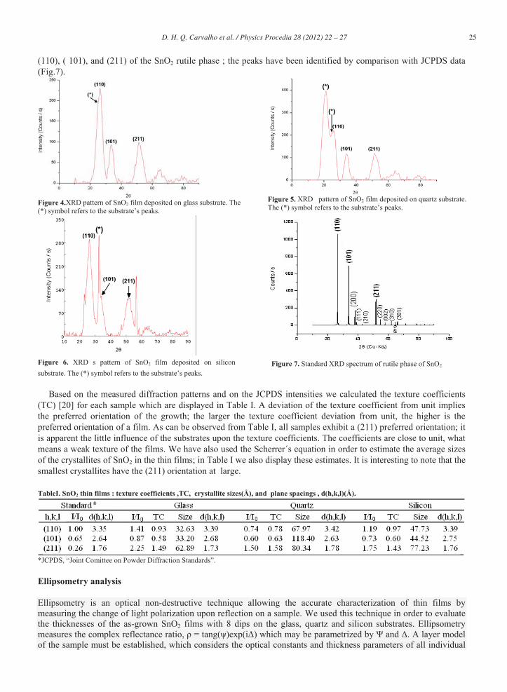
(110), ( 101), and (211) of the SnO2 rutile phase ; the peaks have been identified by comparison with JCPDS data (Fig.7).
Figure 4.XRD pattern of SnO2 film deposited on glass substrate. The (*) symbol refers to the substrate’s peaks.
Figure 5. XRD pattern of SnO2 film deposited on quartz substrate. The (*) symbol refers to the substrate’s peaks.
Figure 6. XRD s pattern of SnO2 film deposited on silicon substrate. The (*) symbol refers to the substrate’s peaks.
Figure 7. Standard XRD spectrum of rutile phase of SnO2
Based on the measured diffraction patterns and on the JCPDS intensities we calculated the texture coefficients (TC) [20] for each sample which are displayed in Table I. A deviation of the texture coefficient from unit implies the preferred orientation of the growth; the larger the texture coefficient deviation from unit, the higher is the preferred orientation of a film. As can be observed from Table I, all samples exhibit a (211) preferred orientation; it is apparent the little influence of the substrates upon the texture coefficients. The coefficients are close to unit, what means a weak texture of the films. We have also used the Scherrer´s equation in order to estimate the average sizes of the crystallites of SnO2 in the thin films; in Table I we also display these estimates. It is interesting to note that the smallest crystallites have the (211) orientation at large. TableI. SnO2 thin films : texture coefficients ,TC, crystallite sizes(Å), and plane spacings , d(h,k,l)(Å).
*JCPDS, “Joint Comittee on Powder Diffraction Standards”. Ellipsometry analysis
Ellipsometry is an optical non-destructive technique allowing the accurate characterization of thin films by measuring the change of light polarization upon reflection on a sample. We used this technique in order to evaluate the thicknesses of the as-grown SnO2 films with 8 dips on the glass, quartz and silicon substrates. Ellipsometry measures the complex reflectance ratio, = tang( )exp(i ) which may be parametrized by and . A layer model of the sample must be established, which considers the optical constants and thickness parameters of all individual
26 D. H. Q. Carvalho et al. / Physics Procedia 28 ( 2012 ) 22 – 27
layers. Using an iterative procedure, unknown optical constants and/or thickness parameters are varied, and and values are calculated using the Fresnel equation the calculated and values which match the experimental data lead to the optical constants and thickness parameters of the sample. An equipment Wooller , model M2000 , having a wavelength range 245-1690 nm, was used to make measurements at three angles The corresponding ellipsometric parameters , and , were determined, thus leading to the values of the film thicknesses . The substrates were modeled using uncoated samples and the thickness was determined by linear regression analysis. The experimental and data and the corresponding model fits are shown in Fig.8.
Figure 8. Experimental ellipsometric data for (up) and ( down) vs. wavelength, with the model fits (dotted lines), taken at three different angles (colors), for SnO2 films deposited on quartz substrate after 8 dips.
It is worth mentioning that the model does not provide a perfect fit for the experimental data, probably because of the use made of bulk optical constants to model the SnO2 film. The fit of the and curves as a function of wavelength were carried out by means of three Lorentzian curves. Once the adjustments were made, a comparison between the experimental curves (solid lines) and the theoretical model ones (dotted lines) provided a theoretical best fit and the corresponding stored theoretical data permitted to obtain the value of the thickness of each film . The SnO2 film thicknesses determined by means of this kind of analysis were 123.59 nm, 156.89nm, and 97.88nm for glass, quartz, and silicon substrates, respectively. Mössbauer spectroscopy
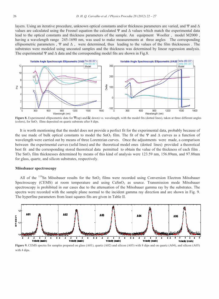
All of the 119Sn Mössbauer results for the SnO2 films were recorded using Conversion Electron Mössbauer
Spectroscopy (CEMS) at room temperature and using CaSnO3 as source. Transmission mode Mössbauer spectroscopy is prohibited in our cases due to the attenuation of the Mössbauer gamma ray by the substrates. The spectra were recorded with the sample plane normal to the incident gamma ray direction and are shown in Fig. 9. The hyperfine parameters from least squares fits are given in Table II.
Figure 9. CEMS spectra for samples prepared on glass (A01), quartz (A02) and silicon (A03) with 8 dips and on quartz (A04), and silicon (A05) with 4 dips.

D. H. Q. Carvalho et al. / Physics Procedia 28 ( 2012 ) 22 – 27 27
Figure 10. CEMS spectra for samples prepared on quartz (A02) and silicon (A03), with 8 dips, and the corresponding quadrupole splitting distributions P ( ).
Table II.Hyperfine parameters, isomer shift, , quadrupole splitting, , line width, , and quadrupole moment Q.
As anticipated by the literature, the isomer shifts and quadrupole splits are close to the values for the CaSnO3 source [21]. The distribution of the quadrupole splits, Fig. 10, exhibit a distortion of the electron density around the nucleus , probably associated to the presence of tin atoms in states other than the Sn+4 in the lattice of the SnO2 crystal . Also shown in Table II are the quadrupole moments, Q, as obtained by combining the experimental values and the theoretical electric field gradient, Vzz, calculated for the bulk. These values for the several samples are very close to the experimental value Q = 10.9 ± 0.8 fm2 [22]. Final remarks
The stoichiometry of tin dioxide was verified for all samples by XPS which also revealed very small quantities of
chlorine and carbon as contaminants.The XDR diagrams recorded under grazing incidence showed that the layers are polycrystaline and that the peak intensities correspond fairly well to the intensities given by the JCPDS card. This is indicative of a random crystallite orientation (i.e. powder-like sample), though the (110) orientation be preferred. After eight dips, the obtained films were ~ 100 nm thick, as measured by ellipsometry. The Mössbauer spectra showed that SnO2 is present in the films as single phase, the isomer shift is close to that of CaSnO3, as expected, and the experimental/theoretical quadrupole moment obtained for the tin nucleus is close to the experimental value reported in the literature.
References
1. Tsirlina GA, Roginskaya YuE, Postovalova GG, Vassiliev SYu Russ J Electrochemistry 35, 1385. (1999). 2. Courtney IA, Dahl JR. J Electrochem Soc 144, 2045(1997); 144, 2943 (1997). 3.Zhu J, Lu Zh, Aruna ST, Aurbach D, Gedanken A Chem Matter 12,2557 (2000) . 4. A. Nuruddin and J.R. Abelson, Thin Solid Films 394, 49 (2001). 5. Barreca, D.; Garon, S.; Zanella, P.; Tondello, E. J. Phys. IV France, 9, 667(1999). 6. Matko, I.; Gaidi, M.; Hazemann, J. L.; Chenevier, B.; Labeau, M. Sensors Actuators 7. Gaggiotti, G.; Galdikas, A.; Kaiulis S.; Mattogno, G.; Setkus, A. Sensors Actuators B, 24 25, 516 519 (1995). 8. Schweizer-Berberich, M.; Zheng, J. G.; Weimar, U.; Göpel, W.; Bârsan, N.; Pentia, E.; Tomescu, A. Sensors Actuators B, 31, 71 75 (1996). 9. Williams, G.; Coles, G. S. V. MRS Bull., 24 (6), 25 29 (1999). 10. Brinker, C. J.; Scherer, G. W. In Sol Gel Science: The Physics and Chemistry of Sol GelProcessing; Academic Press: New York, 1990. 11 Varghese, O. K.; Mahlotra, L. K.; Sharma, G. L. Sensors Actuators B, 55, 161 165(1999). 12.M. Acciarri, C. Canevali, C. M. Mari, M. Mattoni, R. Ruffo, R. Scotti, and F. Morazzoni,D. Barreca, L. Armelao, and E. Tondello , E. Bontempi and L. E. Depero .Chem. Mater, 15 , 2646 (2003).13. Shimizu, Y.; Egashira, M. MRS Bull., 24, 18 (1999). 14. Alfredo R. M. Oliveira, Aldo J. G. Zarbin. Quim.Nova , 28,1(2005). 15J. Grim,D.Bessarov, W. Maier, S. Storck and R.D.Saderson. Desalination 115,295(1998). 16. N.J.Arfsten, J.Non. Cryst. Solids, 63,243(1984). 17. Hohenberg,P. and Kohn, W., Phys.Rev.136,B864(1964),; Kohn,W and Sham,L.J., Phys.Rev. 140,A1133(1965). 18.Blaha,P.,Schwarz,K., Sorantin,P., and Trickey,S.B.,Comput.Phys.Commun.59,399(1990),. 19. N. Ikeo. Handbook of X-ray photoelectron spectroscopy. JEOL, 1991. 20.Moholkar, A. V.; Pawar, S. M.; Rajpure, K. Y.; Patil, P. S.; Bhosale J. of Phys. and Chem. of Solids, 68, 1981, (2007). 21. M.Methfessel, C.O.Rodriguez, O.K.Anderson.Phys.Rev.B40, 2009(1989). 22. H.Haas, M.Menningen, H.Andreasen,S. Damgaard, H. Grann,F.T. Pedersen,J.W. Petersen , andG.Weyer, Hyp.Interact. 15/16(1983).