swtw2014 sv tcl 3d tsv cu pillar challenges experience akn
TRANSCRIPT

3D TSV Cu Pillar Probing Challenges & Experience
3次元TSVプロービングの課題と経験
3D TSV Cu Pillar Probing Challenges & Experience
3次元TSVプロービングの課題と経験
Ray Grimm/Mohamed HegazySV TCL – An SV Probe Company
Linjianjun (David) Hi‐Silicon
Rick ChenSPIL

The Challenges
22

Cu Pillar Bump Reliability Shear TestCu Pillar Bump Reliability Shear TestEach Assembly/Packaging house has done many DOEs & optimized their bump geometry, UBM, PI thickness to optimize reliability.
Reliability Test…
CornerCorner CornerCorner
Bump StructureBump StructureBump Structure
Fig 1. Stress Point after FC Attach ReflowFig 1. Stress Point after FC AttachFig 1. Stress Point after FC Attach ReflowReflow Fig 2. Stress Point After AssemblyFig 2. Stress Point After AssemblyFig 2. Stress Point After Assembly33

2525µµmm
7070µµmm
For Bump Shear Test, the wedge force at 20%~30% of Total Height of PillarEg.TH= 80µm, shear test start at 25µm & the other to solder cap at 70µm.
After the shear test was complete, the next step is for TCT Thermal Cycle for 1000 cycles, and results were observed to be passing. If the geometry is not optimized then fractures will show up on the stress points. Same concept was performed if probing on 2 different conditions…
Shear Force TestSpec >7mgf/µm2
Shear Force TestShear Force TestSpec >7mgf/Spec >7mgf/µµmm22
Prob
eProb
e
shear force apply on stress point.
shear force shear force apply on apply on stress stress point.point.
Prob
eProb
e
Cu‐Pillar Bump Probing w/Staggered ProbeCu‐Pillar Bump Probing w/Staggered ProbeHigh Risk of Peeling & Fracture Failures:剥がれ、破断不良のリスクHigh Risk of Peeling & Fracture Failures:剥がれ、破断不良のリスク
Bump shear tests were performed as per the JEDEC standards (JEDD22-B117).:バンプせん断試験は、JEDEC規格(JEDD22-B117)に従って実施した。
Optimum High Risk
44

The SV‐TCL Experience
55

Recap of previous activitiesRecap of previous activities
•Case #1 :2010 Copper Pillar & Bump Probing– Engineering lab tests
•Case #2: 2012 50µm Pitch Array w/LogicTouch™– First trial on customer wafer
66

Case #1 ‐ Copper Pillar & Bump ProbingCase #1 ‐ Copper Pillar & Bump Probing• Internal Work to Study Contact
Behavior of Cu‐pillar Bumps at 60µm Pitch with Various Solder Cap Materials: 60umピッチバンプ: – Cu‐pillar with Eutectic Solder Cap:共晶はんだ– Cu‐pillar with Lead‐free Solder Cap:鉛フリーはんだ– Cu‐pillars
• Demonstrated :実証– Critical stress points and mechanical failure mechanisms
of the probe card as well as the Cu Pillar :機械的不良– Critical parameters to achieve reliable and stable
contact to different configurations :問題となるパラメータ
• Presented at SWTW 2010
Eutectic Cap
Lead Free Cap
Direct on Cu
77

Case #2 – 50µm Pitch Array w/LogicTouch™Case #2 – 50µm Pitch Array w/LogicTouch™
Co‐presented with ASE at SWTW 2012CoCo‐‐presented with ASE at SWTW 2012presented with ASE at SWTW 2012
88

So where have we gone since SWTW 2010 and 2012 ?
SWTW2010,2012以後の結果
So where have we gone since SWTW 2010 and 2012 ?
SWTW2010,2012以後の結果
99

Case#3 Production Reliability DOEHuawei/Hi‐Silicon/SPIL
Cu Pillar + Solder Cap Probe Mark DOEMobile Chip Hi3620
1010

DOE set up
1111

Probe Mark Size Sampling Plan
1212

Probe Mark Size Analysis
1313

RVSI InspectionRobotic vision bump inspection system
1414

Die Test Results
• No Bin shifting observed
• Stability shown even with increasing TD and OD
1515

Probe Mark SEM Verification
1616

Ion Miller Verification of Low K Layer
• No Low K cracking observed
1717

X‐Ray Results• No Abnormality observed
1818

C‐SAM ResultsC‐Mode Scanning Acoustic Microscope
• No Abnormality observed
1919

T‐Ray ResultsTerahertz Radiation
• No Abnormality observed
2020

Current Status :現状
• High yield observed :高いイールド
– 98% Die yield
– 99% Mechanical bump damage yield
• 2 more Devices successfully completed reliability testing:追加2デバイスの信頼性テスト良好
• More than 10 devices are in full production:10以上のデバイスを量産使用
2121

Lifetime study versus actual針寿命の考察結果
Lifetime study versus actual針寿命の考察結果
2222

Probe mark and expected life time with aggressive clean Trio2milFlat pitch@80um
Customer Patrs_ID Device # Close die Test Site
Initial tip extension
Current Tip
extension
CurrentTDs
TDs per mil of tip
extension loss
Life expectancy in TDs
HIS HI0007 HI-3516 2 1317 2 18.26 16.67 135,736 85,369 875,881
1-Obtain initial and current tip extension and TDs2-Obtain TDs per mil of tip extension loss
3-Obtain life expectancy based on available tip extension and TDs per mil of tip extension loss
23

Actual life time with optimized clean Trio2milFlat pitch@80um
1,921,787 TDs 2 Million TDs !
24
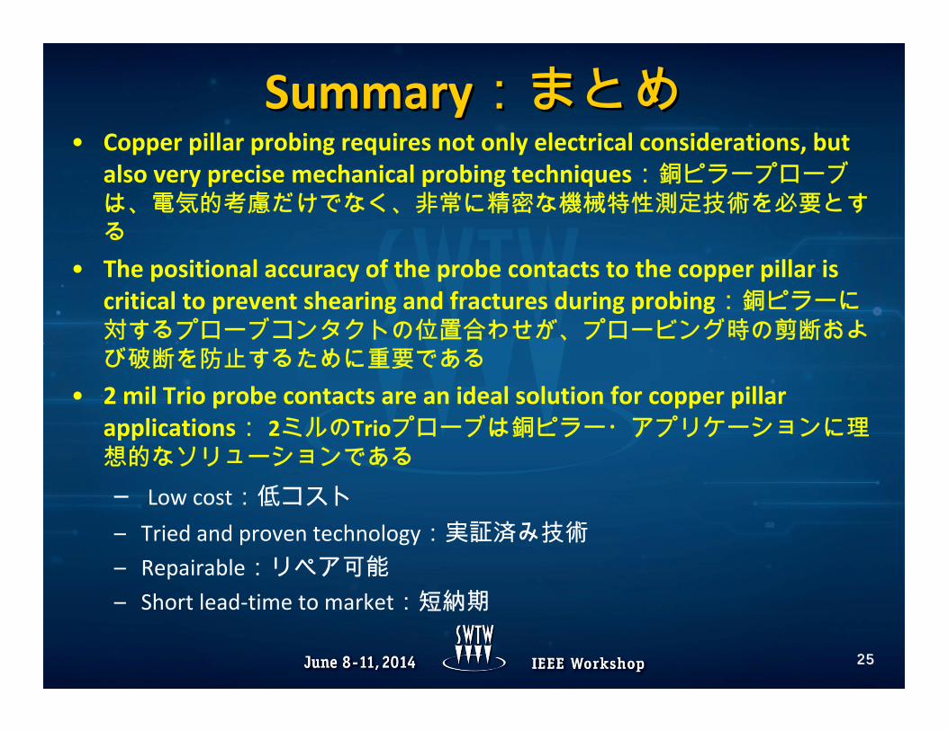
Summary:まとめSummary:まとめ• Copper pillar probing requires not only electrical considerations, but
also very precise mechanical probing techniques:銅ピラープローブは、電気的考慮だけでなく、非常に精密な機械特性測定技術を必要とする
• The positional accuracy of the probe contacts to the copper pillar is critical to prevent shearing and fractures during probing:銅ピラーに対するプローブコンタクトの位置合わせが、プロービング時の剪断および破断を防止するために重要である
• 2 mil Trio probe contacts are an ideal solution for copper pillar applications: 2ミルのTrioプローブは銅ピラー・アプリケーションに理想的なソリューションである– Low cost:低コスト– Tried and proven technology:実証済み技術– Repairable:リペア可能– Short lead‐time to market:短納期
2525