switching rules either a+ or a– is always closed, but never at the same time * either b+ or b–...
TRANSCRIPT

Switching rules
•Either A+ or A– is always closed, but never at the same time *
•Either B+ or B– is always closed, but never at the same time *
*same time closing would cause a short circuit from Vdc to ground
Corresponding values of Va and Vb
• A+ closed, Va = Vdc
• A– closed, Va = 0
• B+ closed, Vb = Vdc
• B– closed, Vb = 0
H BRIDGE
Vdc
Load
A+ B+
A– B–
Va Vb

Corresponding values of Vab
•A+ closed and B– closed, Vab = Vdc
•A+ closed and B+ closed, Vab = 0
•B+ closed and A– closed, Vab = –Vdc
•B– closed and A– closed, Vab = 0
•The free wheeling diodes permit current to flow even if all switches did open
•These diodes also permit lagging currents to flow in inductive loads
H BRIDGE
Vdc
Load
A+ B+
A– B–
Va Vb

Figure 1. Vcont , –Vcont , and Vtri
Vcont –VcontVtri
But is a square wave output good enough? Not for us! Sinusoidal load voltage is usually the most desirable. But how do we approximate a
sinusoidal output with only three states (+Vdc, –Vdc, 0) ?
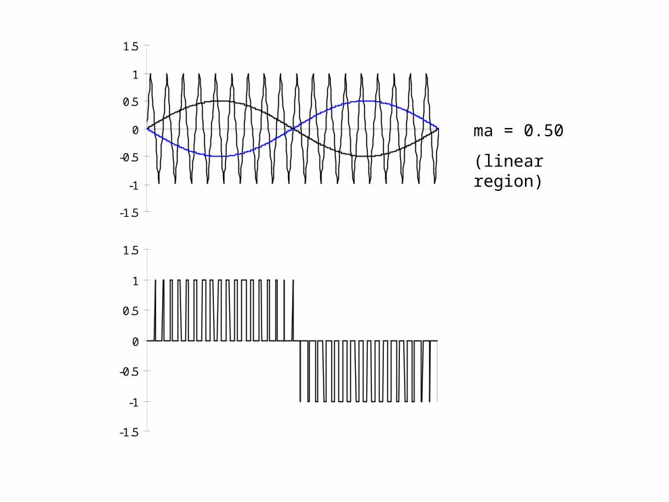
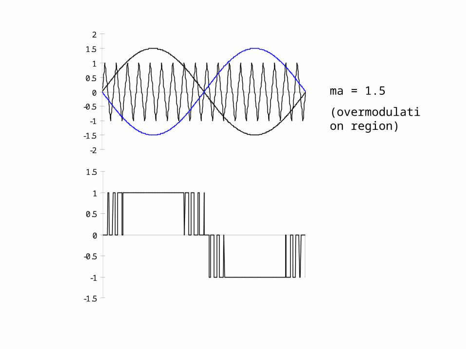
The answer: Unipolar PWM modulation
Vcont > Vtri , close switch A+, open switch A– , so voltage Va = Vdc
Vcont < Vtri , open switch A+, close switch A– , so voltage Va = 0
–Vcont > Vtri , close switch B+, open switch B– , so voltage Vb = Vdc
–Vcont < Vtri , open switch B+, close switch B– , so voltage Vb = 0

A+ closed, A– open, so Va in Figure 2 = Vdc. Else A– closed, A+ open, so Va = 0.
B+ closed, B– open, so Vb in Figure 2 = Vdc. Else B– closed, B+ open, so Vb = 0.

Vdc
Idealized Load Voltage (Va – Vb) Waveform–Vdc
0
-1.5
-1
-0.5
0
0.5
1
1.5
-1.5
-1
-0.5
0
0.5
1
1.5
ma = 0.50
(linear region)
-2
-1.5
-1
-0.5
0
0.5
1
1.5
2
-1.5
-1
-0.5
0
0.5
1
1.5
ma = 1.5
(overmodulation region)

Figure 6. Variation of RMS value of no-load fundamental inverteroutput voltage (V1rms
) with ma
ma0 1
V1rms
linear overmodulation saturation
asymptotic to square wave value2
4 dcV
2dcV

2mf cluster
4mf cluster
2dcVTable 1. Load voltage harmonic RMS magnitudes with respect to (for large mf )
Harmonicma = 0.2
ma = 0.4
ma = 0.6
ma = 0.8
ma = 1.0
1 (fundamental) 0.200 0.400 0.600 0.800 1.000
2mf ± 1 0.190 0.326 0.370 0.314 0.181
2mf ± 3 0.024 0.071 0.139 0.212
2mf ± 5 0.013 0.033
4mf ± 1 0.163 0.157 0.008 0.105 0.068
4mf ± 3 0.012 0.070 0.132 0.115 0.009
4mf ± 5 0.034 0.084 0.119
4mf ± 7 0.017 0.050
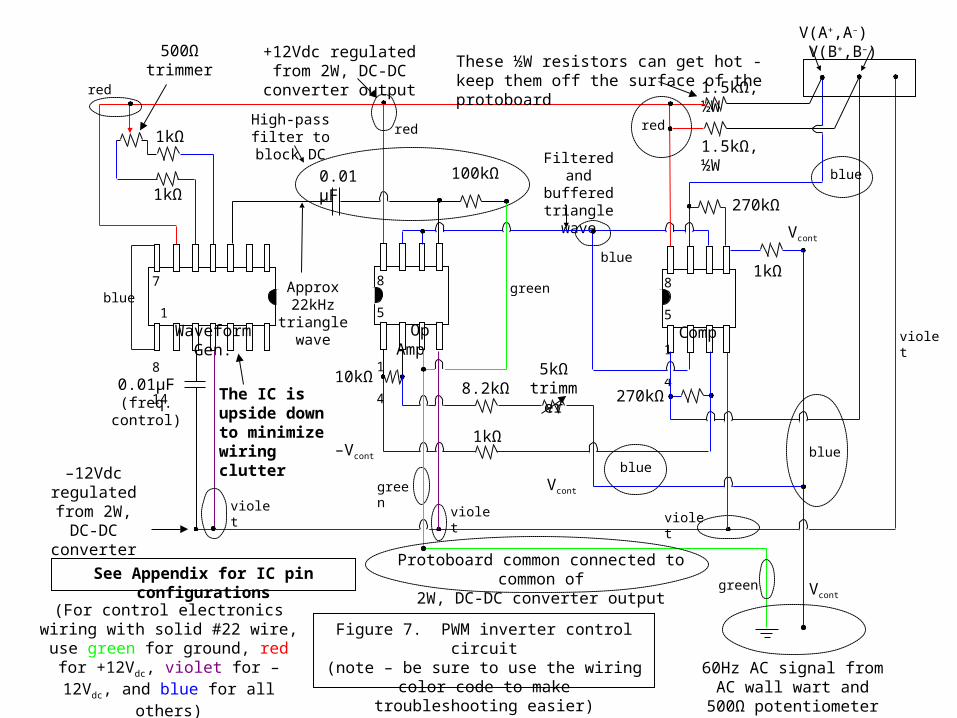
(For control electronics wiring with solid #22 wire, use green for ground, red for
+12Vdc, violet for –12Vdc, and blue for all others)
Figure 7. PWM inverter control circuit(note – be sure to use the wiring color code to
make troubleshooting easier)
8 5
Op Amp1 4
0.01µF(freq. control)
500Ωtrimmer
7 1
Waveform Gen.8 14
1kΩ
1kΩ0.01µF 100kΩ
Approx 22kHztriangle wave
Filtered and buffered
triangle wave
High-pass filter to block DC
8 5
Comp1 4
1.5kΩ, ½W
270kΩ
1.5kΩ, ½W
1kΩ
1kΩ
270kΩ
+12Vdc regulated from 2W, DC-DC converter output
–12Vdc regulated from 2W, DC-DC
converter output
V(A+,A–) V(B+,B–)
Vcont
Vcont
red
green
blue
blue
blue
violet
blue
violet
violet violet
green
red
red
green
The IC is upside down to minimize wiring clutter
These ½W resistors can get hot - keep them off the surface of the protoboard
10kΩ8.2kΩ
5kΩtrimmer
–Vcont
blue
Vcont
60Hz AC signal from AC wall wart and 500Ω potentiometer
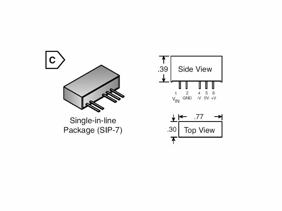
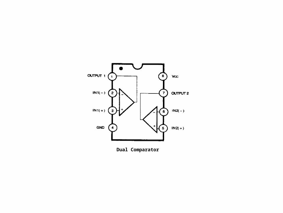
Protoboard common connected to common of2W, DC-DC converter outputSee Appendix for IC pin configurations
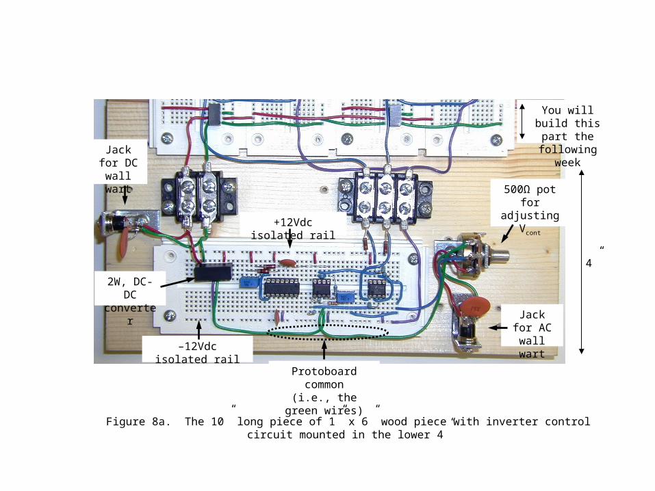
4”
Jack for AC wall
wart
Jack for DC wall
wart
–12Vdc isolated rail
+12Vdc isolated rail
2W, DC-DC converter
500Ω pot for adjusting Vcont
Protoboard common(i.e., the green wires)
Figure 8a. The 10” long piece of 1” x 6” wood piece with inverter control circuit mounted in the lower 4”
You will build this part the following
week

Figure 8b. Zoom-in of protoboardMount triangle wave generator IC upside down to minimize
wiring clutter
2W, DC-DC converter
+12Vdc isolated rail (red)
–12Vdc isolated rail (violet) Protoboard common (i.e., the green wires)
Input from 12Vdc
regulated wall wart
Isolated outputs from 2W, DC-DC converter (red = +12V, violet = –12V,
green = common)
Zoom-in of DC-DC converter

Triangle wave generator

Dual Op Amp
Dual Comparator
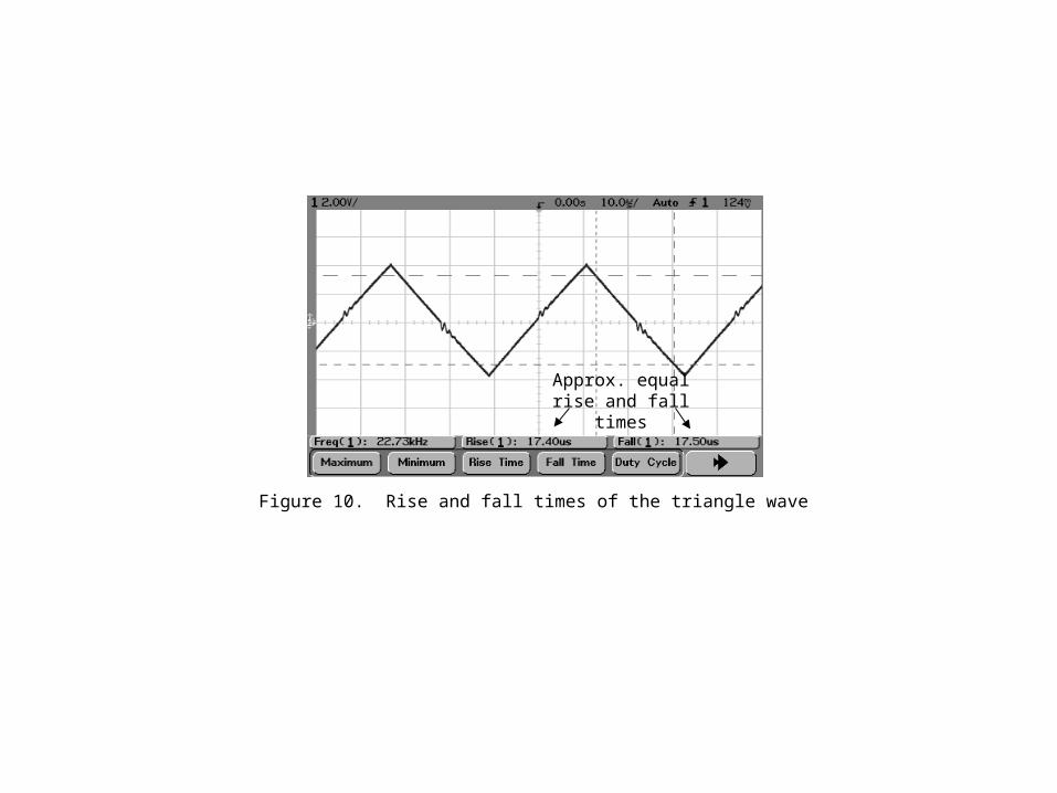
Figure 10. Rise and fall times of the triangle wave
Approx. equal rise and fall times
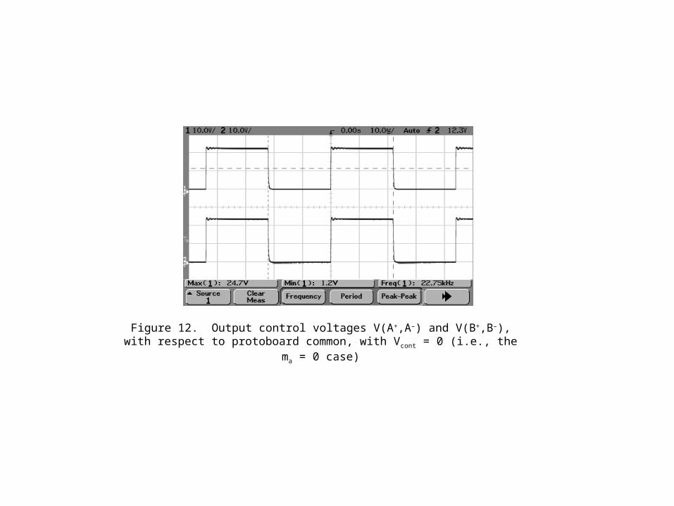
Figure 12. Output control voltages V(A+,A–) and V(B+,B–), with respect to protoboard common, with Vcont = 0 (i.e., the ma = 0 case)

Figure 15. Idealized Vload, with ma just into the overmodulation region
Figure 16. Idealized Vload observed in the scope averaging mode, with ma in the linear region
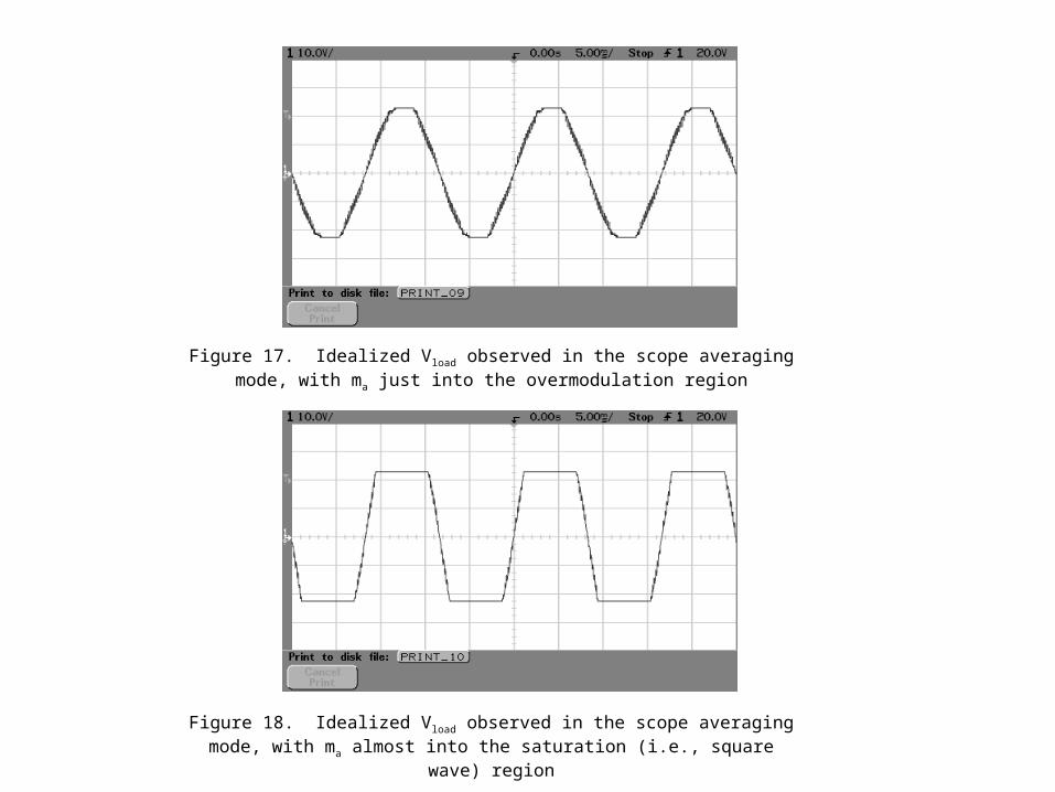
Figure 17. Idealized Vload observed in the scope averaging mode, with ma just into the overmodulation region
Figure 18. Idealized Vload observed in the scope averaging mode, with ma almost into the saturation (i.e., square wave) region
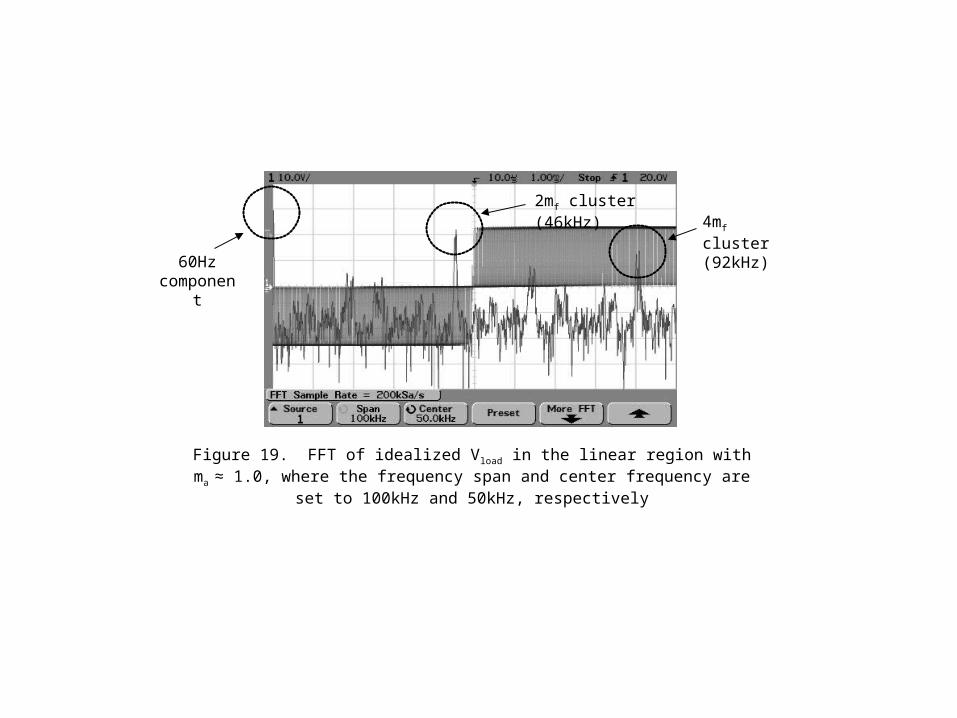
Figure 19. FFT of idealized Vload in the linear region with ma ≈ 1.0, where the frequency span and center frequency are set to 100kHz and 50kHz, respectively
2mf cluster (46kHz)4mf cluster (92kHz)
60Hz component

Figure 23. Near saturation, the 3rd harmonic magnitude is 0.30 of the fundamental
Figure 24. Near saturation, the 5th harmonic magnitude is 0.13 of the fundamental

One firing circuit for each MOSFET, with each firing circuit mounted on a separate protoboard. A– and B– can share a power supply and ground. A+ and B+ must each use separate power supplies and grounds. Do not connect any of these grounds to the ground of the control circuit.
O+ O–
(see Figure 2 for connections)Powered by +12Vdc regulated supply
(isolated from control circuit)
10kΩ
0.1µF10Ω1.2kΩ
MOSFET
G D S
100kΩ
5 4
Opto
8 1
5 4
Driver
8 1
Figure 1. Isolated firing circuit with optocoupler
and gate driver
Outline of protoboard
A+ and B+ use inverting drivers. A– and B– use non-inverting drivers. The optocouplers provide an additional inversion.
green
green
green
blue for A+,B+,violet for A–,B–
blue
blue
red
blue
Grounds (isolated from control circuit)
Wait until next week

Figure 2. Physical layout of firing circuits(A+ opto and driver are powered by a 12Vdc isolated DC-DC
converter. Likewise, B+ has a 12Vdc isolated DC-DC converter. A– and B– are powered by the DC wall wart.)
Individual protoboard for each firing circuit
Optically-isolated firing circuits. Mount drivers near the MOSFETs
A+
FiringA–
FiringB+
FiringB–
Firing
Control Circuit from Previous Lab
Jack for DC wall
wart
O+ O– O+ O– O+ O– O+ O–
V(A+,A–) V(B+,B–)
–12Vdcregulated
blue
blue blue
violet violet
Jack for AC wall
wart
8”
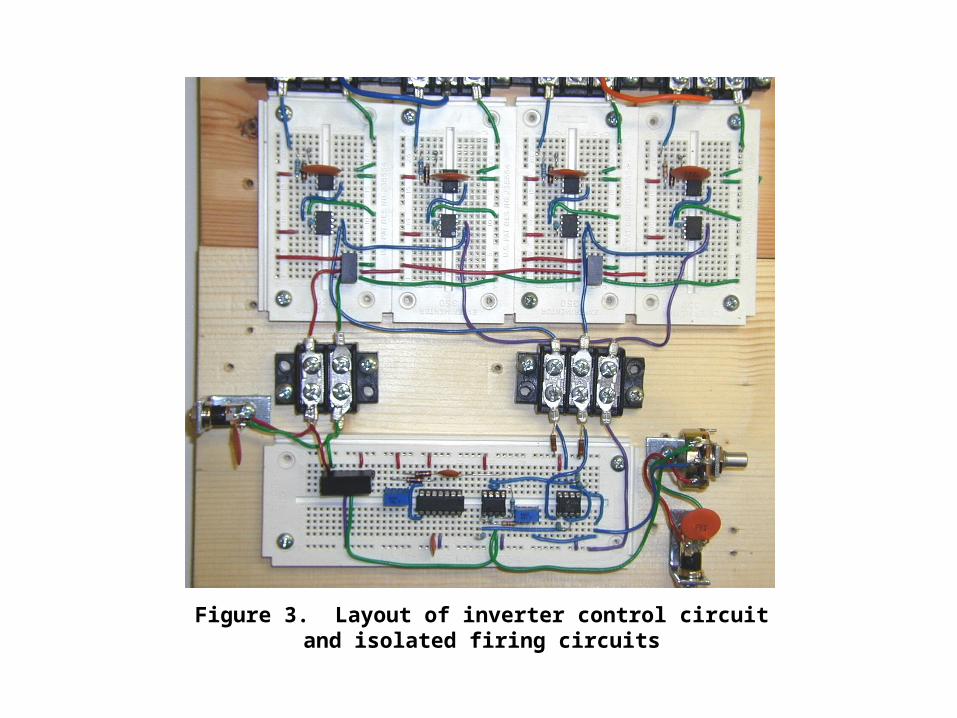
Figure 3. Layout of inverter control circuit and isolated firing circuits
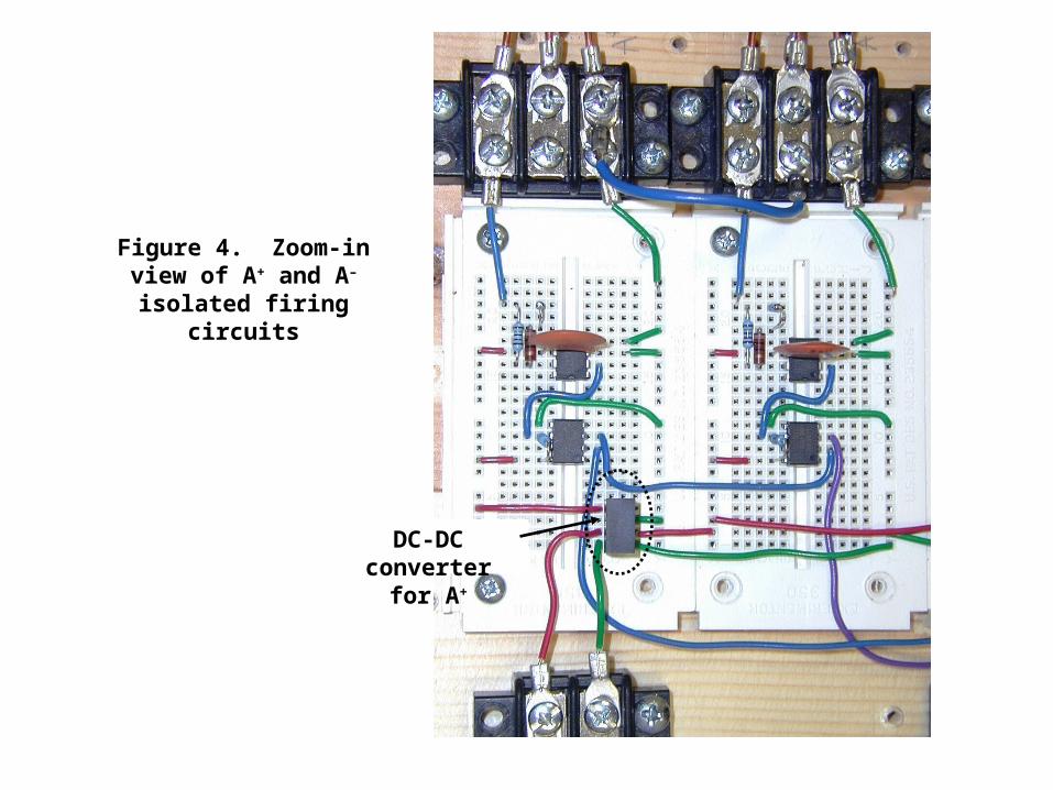
Figure 4. Zoom-in view of A+ and A– isolated
firing circuits
DC-DC converter for A+
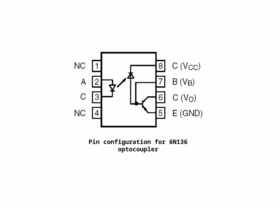
Pin configuration for 6N136 optocoupler

Input from 12Vdc wall wart
Isolated output

V(A+,A–) – V(B+,B–) with control circuit driving optos
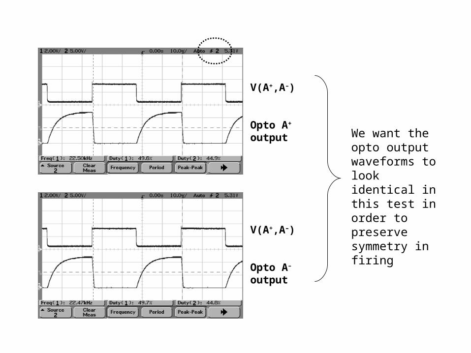
V(A+,A–)
Opto A+ output
V(A+,A–)
Opto A– output
We want the opto output waveforms to look identical in this test in order to preserve symmetry in firing

Opto A+ output
Opto A– output

V(A+,A–)
A+ driver output
V(A+,A–)
A– driver output
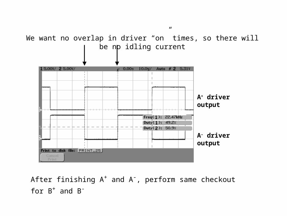
A+ driver output
A– driver output
We want no overlap in driver “on” times, so there will be no idling current
After finishing A+ and A-, perform same checkout for B+ and B-

Figure 1. Physical layout of inverter
MOSFETA+
MOSFETA–
MOSFETB+
MOSFETB–
H-Bridge and Filters
Individual heat sink for each MOSFET
–Vdc
+
–Vac (Output)+
b
a
A+
FiringA–
FiringB+
FiringB–
Firing
Control Circuit from Previous Lab
Jack for DC wall
wart
O+ O– O+ O– O+ O– O+ O–
V(A+,A–) V(B+,B–)
–12Vdcregulated
blue
blue blue
violet violet
Jack for AC wall
wart

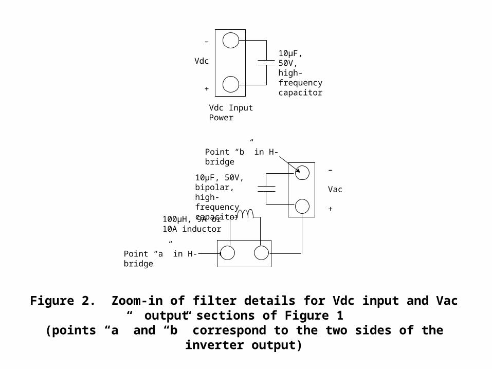
Vdc Input Power
10µF, 50V, high-frequency capacitor
–
Vdc
+
Figure 2. Zoom-in of filter details for Vdc input and Vac output sections of Figure 1(points “a” and “b” correspond to the two sides of the inverter output)
10µF, 50V, bipolar, high-frequency capacitor
100µH, 9A or 10A inductor
–
Vac
+
Point “a” in H-bridge
Point “b” in H-bridge
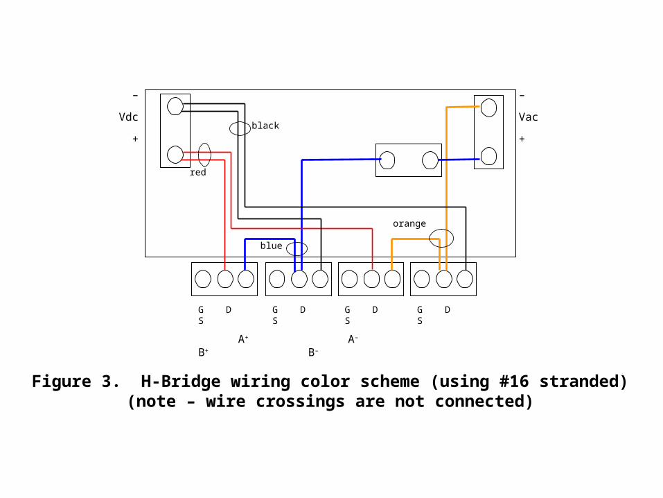
Figure 3. H-Bridge wiring color scheme (using #16 stranded)(note – wire crossings are not connected)
A+ A– B+ B–
G D S G D S G D S G D S
–
Vdc
+
–
Vac
+
red
orange
blue
black

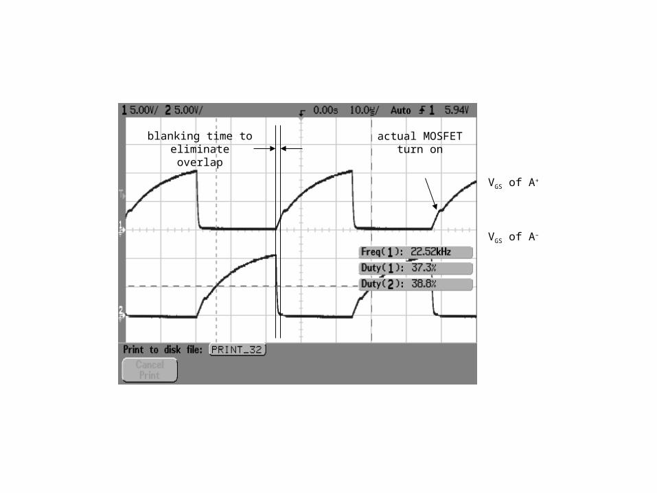
VGS of A+
VGS of A–
blanking time toeliminate overlap
actual MOSFETturn on
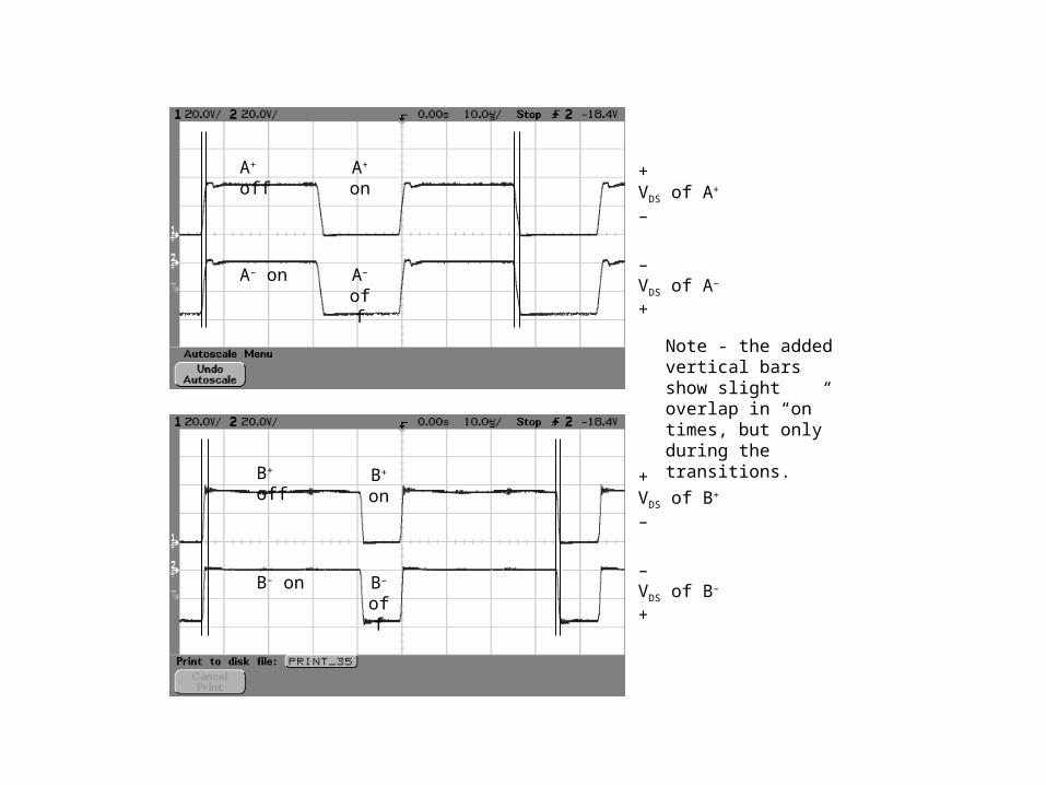
+VDS of A+
–
–VDS of A–
+
A+ off
A– on
A+
on
A–
off
+VDS of B+
–
–VDS of B–
+
B+ off
B– on
B+
on
B–
off
Note - the added vertical bars show slight overlap in “on” times, but only during the transitions.

Vac, without and with filter

Vac with Vcont near saturation