surface treatments as moth-eye structures for a … · central rii cellece i e ccess jsm...
TRANSCRIPT

CentralBringing Excellence in Open Access
JSM Environmental Science & Ecology
Cite this article: GUO KW (2016) Surface Treatments as Moth-eye Structures for a Broadband Anti-Reflective Layer. JSM Environ Sci Ecol 4(2): 1031.
*Corresponding authorKelvii Wei GUO, Department of Mechanical and Biomedical Engineering, City University of Hong Kong, 83 Tat Chee Avenue, Kowloon Tong, Kowloon, Hong Kong, China, Email:
Submitted: 19 July, 2016
Accepted: 04 August, 2016
Published: 06 August, 2016
ISSN: 2333-7141
Copyright© 2016 GUO
OPEN ACCESS
Keywords•Solar cell•Anti-reflectivelayer•Moth-eye•Surface structure•Photolithography•Nanoimprinting•Physical vapor deposition (PVD)•Plasma etching processes
Review Article
Surface Treatments as Moth-eye Structures for a Broadband Anti-Reflective LayerKelvii Wei GUO*Department of Mechanical and Biomedical Engineering, City University of Hong Kong, China
Abstract
To date, fossil fuels once considered inexhaustible, is now being depleted at a rapid rate. Moreover, today’s energy supply is largely responsible for the anthropogenic greenhouse effect, acid rain and other negative impacts on health and the environment. Generally, solar cells/ devices are located in outdoor areas and a protective layer is essential for preventing damage from physical shock and corrosion. However, this protective layer reduces the total conversion efficiency by reflecting sunlight. As a result, the reflection of sunlight needs to be minimized in order to maximize the conversion efficiency. Anti-reflective (AR) coatings are needed to reduce the reflection at the surface.
Nature provides us with a multitude of design solutions finely tuned by natural selection. Bio mimetic, taking the shortcut of ‘‘Learning from Nature’’, transfers optimum designs in nature to technical applications. Herein, we review the methods for surface treatments with mimetic Moth-eye structures for a broadband anti-reflective layer, along with the relevant drawbacks. In the meantime, it is pointed out that the significantly feasible world’s eco-energy for the foreseeable future should not only be realized, but also methods for using the current technologies and their by-products more efficiently should be found correspondingly, especially with minimal environmental or eco-friendly impact.
INTRODUCTIONVoices are being raised for the establishment of an industry
that produces and develops renewable energy (such as hydrogen fuel, solar cell, and wind and ocean energy, especially for the so-called green energy suitable to the friendly environment) from nonconventional sources. Among these renewable energies, solar energy is that beaming light and heat that is generated from the sun, which has been used by human beings since time immemorial. Solar power is used in a widespread of the ever so progressing technologies of the world resulted in an immense amount of constructive and helpful impact on us and on the environment as a whole. Contrasting to the fossil fuels that we consume and use on a daily basis, solar energy does not fabricate the excessively injurious pollutants that are liable for the greenhouse effect which is known to lead to global warming. Meanwhile, it also reduces the quantity of contamination and toxic waste, not to forget pollution that the engendering plants have to produce.
The colorful world around us, or the science beneath, is heavily absorbed in ‘reflection’. However, the fact that the quantum concept, golden to the scientists, lay in a perfectly
absorbing blackbody led us to look at things that suffer, if we may say so, from the lack of reflection. The anti-reflecting materials are interesting not only as high efficiency absorbers but also for the properties that lend them this character. To date, anti-reflective (AR) layers are widely used on the surfaces of solar cells to increase the efficiency of photoelectric conversion [1-3].
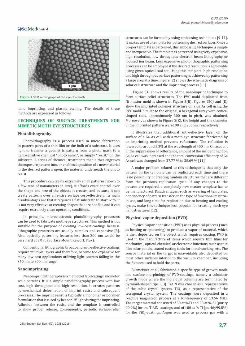
Figure 1 shows SEM images of moth eye surface covered with nipple array [4]. Experimental results proved that such structures substantially reduce the reflection of light and produce an increased transmission within the visible spectrum. The purpose of this fully developed nipple pattern is not only to increase the visual capacity but also to serve as a better camouflage against predators. It was assumed that these structures affect the transmission of light [4].
The discovery of moth-eye nipple patterns shows great promise for creating low-cost broadband anti-reflective surfaces [5-7]. The challenge lies in the actual fabrication of these structures on sub-wavelength scale. For wavelengths 350 nm to 800 nm, the period has to be smaller than 150 nm and height of the structures has to be greater than 400 nm. There are several methods to fabricate such structures including photolithography,
CentralBringing Excellence in Open Access
GUO (2016)Email:
JSM Environ Sci Ecol 4(2): 1031 (2016) 2/7
nano imprinting, and plasma etching. The details of these methods are expressed as follows.
TECHNIQUES OF SURFACE TREATMENTS FOR MIMETIC MOTH-EYE STRUCTURES
Photolithography
Photolithography is a process used in micro fabrication to pattern parts of a thin film or the bulk of a substrate. It uses light to transfer a geometric pattern from a photo mask to a light-sensitive chemical “photo resist”, or simply “resist,” on the substrate. A series of chemical treatments then either engraves the exposure pattern into, or enables deposition of a new material in the desired pattern upon, the material underneath the photo resist.
This procedure can create extremely small patterns (down to a few tens of nanometers in size), it affords exact control over the shape and size of the objects it creates, and because it can create patterns over an entire surface cost-effectively. Its main disadvantages are that it requires a flat substrate to start with, it is not very effective at creating shapes that are not flat, and it can require extremely clean operating conditions.
In principle, microelectronic photolithography processes can be used to fabricate moth-eye structures. This method is not suitable for the purpose of creating low-cost coatings because lithographic processes are usually complex and expensive [8]. Also, optically patterning features less than 300 nm would be very hard at SMFL (Surface Mount Rework Flux).
Conventional lithographic broadband anti-reflective coatings require multiple layers and therefore, become too expensive for many low-cost applications utilizing light sources falling in the 350 nm to 800 nm range.
Nanoimprinting
Nanoimprint lithography is a method of fabricating nanometer scale patterns. It is a simple nanolithography process with low cost, high throughput and high resolution. It creates patterns by mechanical deformation of imprint resist and subsequent processes. The imprint resist is typically a monomer or polymer formulation that is cured by heat or UV light during the imprinting. Adhesion between the resist and the template is controlled to allow proper release. Consequently, periodic surface-relief
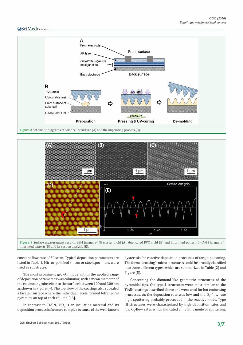
structures can be formed by using embossing techniques [9-11]. It makes use of a template for patterning desired surfaces. Once a proper template is patterned, this embossing technique is simple and inexpensive. The template is patterned using very expensive, high resolution, low throughput electron beam lithography or focused ion beam. Less expensive photolithographic patterning processes can be employed if the desired resolution is achievable using given optical tool set. Using this template, high resolution and high throughput surface patterning is achieved by patterning a large area at a time. Figure (2) shows the schematic diagrams of solar cell structure and the imprinting process [11].
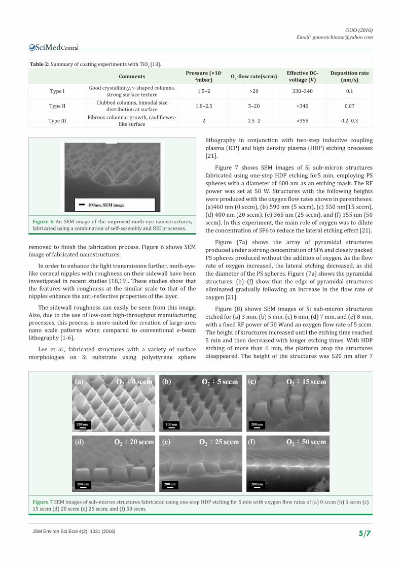
Figure (3) shows results of the nanoimprint technique to form surface-relief structures. The PVC mold duplicated from Ni master mold is shown in Figure 3(B). Figures 3(C) and (D) show the imprinted polymer structure on a Ga As cell using the PVC mold. Similar to the original, a hexagonal array with conical shaped rods, approximately 300 nm in pitch, was obtained. Moreover, as shown in Figure 3(E), the height and the diameter of the imprinted pattern were100 and 250nm, respectively.
It illustrates that additional anti-reflective layer on the surface of a Ga As cell with a moth-eye structure fabricated by an imprinting method prevents reflectance. The reflection is lowered to around 5.3% at the wavelength of 400 nm. On account of the suppression of reflectance, amount of the incident light on Ga As cell was increased and the total conversion efficiency of Ga As cell was changed from 27.77 % to 28.69 % [11].
A major problem related to this technique is that only the pattern on the template can be replicated each time and there is no possibility of creating random structures that are different from the previous replication cycle. If any changes to the pattern are required, a completely new master template has to be manufactured. Disadvantages, such as wearing of templates, dependency of pattern transfer on the type of functional material in use, and long time for replication due to heating and cooling cycles, make this technique less popular for creating moth-eye nanostructures [12].
Physical vapor deposition (PVD)
Physical vapor deposition (PVD) uses physical process (such as heating or sputtering) to produce a vapor of material, which is then deposited on the object which requires coating. PVD is used in the manufacture of items which require thin films for mechanical, optical, chemical or electronic functions, such as thin film solar panels, coated cutting tools for metalworking, etc. The source material or the target is unavoidably also deposited on most other surfaces interior to the vacuum chamber, including the fixtures used to hold the parts.
Burmeister et al., fabricated a specific type of growth mode and surface morphology of PVD-coatings, namely a columnar growth mode where the individual columns are terminated by pyramid-shaped tips [13]. TiAlN was chosen as a representative of the cubic crystal system, TiO2 as a representative of the tetragonal crystal system. The coatings were deposited in a reactive magnetron process at a RF-frequency of 13.56 MHz. The target material consisted of 50 at %Ti and 50 at % Al (purity 99.9%) for the TiAlN-coatings, and of 100 at % Ti (puritiy99.8%) for the TiO2-coatings. Argon was used as process gas with a
Figure 1 SEM micrograph of the eye of a moth.
CentralBringing Excellence in Open Access
GUO (2016)Email:
JSM Environ Sci Ecol 4(2): 1031 (2016) 3/7
Figure 2 Schematic diagrams of solar cell structure (A) and the imprinting process (B).
Figure 3 Surface measurement results: SEM images of Ni master mold (A), duplicated PVC mold (B) and imprinted pattern(C). AFM images of imprinted pattern (D) and its section analysis (E).
constant flow rate of 50 sccm. Typical deposition parameters are listed in Table 1. Mirror-polished silicon or steel specimens were used as substrates.
The most prominent growth mode within the applied range of deposition parameters was columnar, with a mean diameter of the columnar grains close to the surface between 100 and 300 nm as shown in Figure (4). The top view of the coatings also revealed a faceted surface where the individual facets formed tetrahedral pyramids on top of each column [13].
In contrast to TiAlN, TiO2 is an insulating material and its deposition process is far more complex because of the well-known
hysteresis for reactive deposition processes of target poisoning. The formed coating’s micro structures could be broadly classified into three different types, which are summarized in Table (2) and Figure (5).
Concerning the diamond-like geometric structures of the pyramidal tips, the type I structures were most similar to the TiAlN-coatings described above and were used for hot embossing processes. As the deposition rate was low and the O2-flow rate high, sputtering probably proceeded in the reactive mode. Type III structures were characterized by high deposition rates and low O2-flow rates which indicated a metallic mode of sputtering.

CentralBringing Excellence in Open Access
GUO (2016)Email:
JSM Environ Sci Ecol 4(2): 1031 (2016) 4/7
Table 1: Range of deposition parameters used for the deposition of TiAlN- and TiO2-coatings [13].
Material Total pressure (mbar) Reactive gas Gas flow (sccm) RF-power (W) Coating thickness (nm)
TiAlN 1.0–2.0 N2 2–8 500–1000 200–4000
TiO2 1.0–2.5 O2 2–25 1000–2500 600–5000
Figure 4 SEM-micrograph of deposited TiAlN-coating with typical columnar structure and pyramidal tips, top view of coating (a), coatings edge (b). Deposition parameters: p =1e-2 mbar, N2 flow=2.5 sccm, P=500 W.
Figure 5 SEM-micrographs of typical examples of deposited TiO2-coatings. Top: type I structures (a,b) middle: type II structure (c,d) bottom: type III structure (e,f).
Type II coatings were often observed for unstable processes and difficult to reproduce [13].
Results indicated that hot embossed into one side of PMMA-sheets through steel specimen coated with TiAlN and TiO2, the coatings were replicated into PMMA sheets and led to a significant reduction of the sheet’s reflectivity.
Low-cost manufacturing of stochastic surface-relief structures is possible by using physical vapor deposition (PVD) processes [14], which also can be seen from Figs 4 and 5. These surface-relief structures can then be used as templates for creating subsequent low-cost large-area moth-eye patterns by means of embossing. This technique is similar to nano imprinting and hence the disadvantages of fabricating nanostructures using nano imprinting also hold true for this technique.
Plasma etching processes
Initially, plasma etching is a form of plasma processing used to fabricate integrated circuits. It involves a high-speed stream of glow discharge (plasma) of an appropriate gas mixture being shot (in pulses) at a sample. The plasma source known as etch species can be either charged (ions) or neutral (atoms and radicals). During the process, the plasma will generate volatile etch products at room temperature from the chemical reactions between the elements of the material etched and the reactive species generated by the plasma. Eventually the atoms of the shot element embed themselves at or just below the surface of the target, thus modifying the physical properties of the target.
Nanostructure formation is possible using plasma etching processes [15-17]. Biomimetic moth-eye nanostructures to serve as an anti-reflective layer have been tried for last few decades [15-19]. The material that needs to be patterned is deposited on the substrate. A thinner layer of a masking material is deposited such that a conformal coating of this layer is avoided and instead deposition of nano particle clusters is attained. When the base
layer is etched with nano particles as mask, the nano scale pattern is transferred on the base layer. If these processes are performed at specific deposition and etch conditions, these nano scale patterns will result in grass-like structures. Such structures behave as broadband anti-reflective coatings, similar to the moth-eye corneal nipple structures [20].
A combination of self-assembly and reactive-ion etching (RIE) was employed to fabricate the improved nanostructures. A thin layer of base material was deposited using the sol-gel technique on a glass substrate. A high refractive index silicon nitride layer was deposited on the base layer. A masking layer of silicon dioxide nano particles of 400 nm is coated on the nitride layer to function as an etch mask. RIE of silicon nitride with oxide etch mask creates desired nanostructures with side wall roughness. The unwanted silicon oxide nano particles are finally
CentralBringing Excellence in Open Access
GUO (2016)Email:
JSM Environ Sci Ecol 4(2): 1031 (2016) 5/7
Table 2: Summary of coating experiments with TiO2 [13].
Comments Pressure (×10-
2mbar) O2-flow rate(sccm) Effective DC-voltage (V)
Deposition rate (nm/s)
Type I Good crystallinity, v-shaped columns, strong surface texture 1.5–2 >20 330–340 0.1
Type II Clubbed columns, bimodal size distribution at surface 1.8–2.5 5–20 >340 0.07
Type III Fibrous columnar growth, cauliflower-like surface 2 1.5–2 >355 0.2–0.3
Figure 6 An SEM image of the improved moth-eye nanostructures, fabricated using a combination of self-assembly and RIE processes.
Figure 7 SEM images of sub-micron structures fabricated using one-step HDP etching for 5 min with oxygen flow rates of (a) 0 sccm (b) 5 sccm (c) 15 sccm (d) 20 sccm (e) 25 sccm, and (f) 50 sccm.
removed to finish the fabrication process. Figure 6 shows SEM image of fabricated nanostructures.
In order to enhance the light transmission further, moth-eye-like corneal nipples with roughness on their sidewall have been investigated in recent studies [18,19]. These studies show that the features with roughness at the similar scale to that of the nipples enhance the anti-reflective properties of the layer.
The sidewall roughness can easily be seen from this image. Also, due to the use of low-cost high-throughput manufacturing processes, this process is more-suited for creation of large-area nano scale patterns when compared to conventional e-beam lithography [1-6].
Lee et al., fabricated structures with a variety of surface morphologies on Si substrate using polystyrene sphere
lithography in conjunction with two-step inductive coupling plasma (ICP) and high density plasma (HDP) etching processes [21].
Figure 7 shows SEM images of Si sub-micron structures fabricated using one-step HDP etching for5 min, employing PS spheres with a diameter of 600 nm as an etching mask. The RF power was set at 50 W. Structures with the following heights were produced with the oxygen flow rates shown in parentheses: (a)460 nm (0 sccm), (b) 590 nm (5 sccm), (c) 550 nm(15 sccm), (d) 400 nm (20 sccm), (e) 365 nm (25 sccm), and (f) 155 nm (50 sccm). In this experiment, the main role of oxygen was to dilute the concentration of SF6 to reduce the lateral etching effect [21].
Figure (7a) shows the array of pyramidal structures produced under a strong concentration of SF6 and closely packed PS spheres produced without the addition of oxygen. As the flow rate of oxygen increased, the lateral etching decreased, as did the diameter of the PS spheres. Figure (7a) shows the pyramidal structures; (b)–(f) show that the edge of pyramidal structures eliminated gradually following an increase in the flow rate of oxygen [21].
Figure (8) shows SEM images of Si sub-micron structures etched for (a) 3 min, (b) 5 min, (c) 6 min, (d) 7 min, and (e) 8 min, with a fixed RF power of 50 Wand an oxygen flow rate of 5 sccm. The height of structures increased until the etching time reached 5 min and then decreased with longer etching times. With HDP etching of more than 6 min, the platform atop the structures disappeared. The height of the structures was 520 nm after 7

CentralBringing Excellence in Open Access
GUO (2016)Email:
JSM Environ Sci Ecol 4(2): 1031 (2016) 6/7
Figure 8 SEM images of sub-micron structures etched for durations of (a) 3 min (b) 5 min (c) 6 min (d) 7 min and (e) 8 min.
min of etching. The above experiments demonstrate that the one-step HDP etching limited the height of structures due to the PS spheres becoming detached from the top of the structures.
To enhance the height of the structures, cylindrical structures on the Si substrate were fabricated at first using ICP etching in a gas mixture of SF6 and C4F8.During this etching process, SF6 was used for etching and C4F8 plasma free radicals formed a polymer layer that protected the sidewall, which would otherwise have been subject to sputtering damage.
Figure 9 shows the array of cylinders after 3 min of etching, with structures of 620 nm in height. Following fabrication of the cylindrical structures, the Si substrate was subjected to HDP etching to produce arrays with higher paraboloidal and pyramidal structures. Figure10 shows SEM images of sub-micron structures fabricated using a two-step etching process. The heights of the structures in each array were 609 nm, 584 nm, 795 nm, and 760 nm, respectively [21].
Results show that the sub micron pyramidal structure has the best anti-reflection performance with the average reflectance effectively suppressed to below 1%across the spectral range of 300–1200 nm.
CONCLUSIONThe methods for surface treatments with mimetic moth-
eye structures for a broadband anti-reflective layer, such as
Figure 9 SEM images of sub-micron cylinder array at 3 min of ICP etching.
photolithography; nano imprinting; physical vapor deposition (PVD); plasma etching processes, have been reviewed. It is well known that in microelectronic device fabrication, the focus is almost always on eliminating impurities at each step. Clean substrates and proper film deposition processes shall be desired to fabricate reliable devices with very high yield. A variety of films shall be deposited or thermally grown on given substrate more easily. As cleaner and low-defect films are sought, process engineers and industry professionals shall have come up with film deposition guidelines that yield in very low particulate defect densities and film imperfections by avoiding certain operating conditions. Therefore, as for a broadband anti-reflective layer with moth-eye structures, the relevant techniques shall not only be simpler, the operation shall but also be definitely easier to fabricate the anti-reflective layer with precisely mimetic moth-eye structures, which have more potential applications to improve photoelectric properties of the electrode usually applied in chemical biology [22-28]. Moreover, in accordance with the environmental requirements, the harmful substances applied in the processing, such as the etching chemicals, reaction gases,
Figure 10 SEM images of sub-micron structures fabricated using a two-step etching process.

CentralBringing Excellence in Open Access
GUO (2016)Email:
JSM Environ Sci Ecol 4(2): 1031 (2016) 7/7
shall be consumed efficiently or diminished to the lower level, and replaced by other substitutes in the end.
REFERENCES1. Hassani NI, Rezaei M, Brown R, Jang SJ, Turay A, Fathipour V, et al.
Efficient luminescence extraction strategies and anti-reflective coatings to enhance optical refrigeration of semiconductors. J Luminescence. 2016; 170: 841-854.
2. Chattopadhyay S, Huang YF, Jen YJ, Ganguly A, Chen KH, Chen LC. Anti-reflecting and photonic nanostructures. Materials Sci Eng R. 2010; 69: 1-35.
3. Bruynooghe S, Tonova D, Sundermann M, Koch T, Schulz U. Antireflection coatings combining interference multilayers and a nanoporous MgF2 top layer prepared by glancing angle deposition. Surface & Coatings Tech. 2015; 267: 40-44.
4. Achtelik J, Sievers W, Lindner JK. Biomimetic approaches to create anti-reflection glass surfaces for solar cells using self-organizing techniques. Materials Sci Eng B. 2013; 178: 635-638.
5. Watson GS, Watson JA. Natural nano-structures on insects-possible functions of ordered arrays characterized by atomic force microscopy. Applied Surface Sci. 2004; 235: 139-144.
6. Forberich K, Dennler G, Scharber MC, Hingerl K, Fromherz T, Brabec CJ. Performance improvement of organic solar cells with moth eye anti-reflection coating. Thin Solid Films. 2008; 516: 7167-7170.
7. Joki-Korpela F, Karvinen J, Päivänranta B, Pakkanen TT. Hydrophobic and oleophobic anti-reflective polyacrylate coatings. Microelectronic Eng. 2014; 114: 38-46.
8. Liu SJ, Chen WA. Nano featured anti-reflective films manufactured using hot roller imprinting and self-assembly nano sphere lithography. Optics &Laser Tech. 2013; 48: 226-234.
9. Suzuki K, Smith BW. Microlithography: Science and Technology. 2nd Edn. 2007.
10. Nam MW, Lee JJ, Lee KK. Efficiency improvement of solar cells by importing micro dome-shaped anti-reflective structures as a surface protection layer. Microelectronic Eng. 2011; 88: 2314-2318.
11. Han KS, Shin JH, Yoon WY, Lee H. Enhanced performance of solar cells with anti-reflection layer fabricated by nano-imprint lithography. Solar Energy Materials & Solar Cells. 2011; 95: 288-291.
12. Wolfe DB, Love JC, Whitesides GM. Nanostructures Replicated by Polymer Molding. Dekker Encyclopedia of Nano Sci and Nanotech. 2004.
13. Burmeister F, Schäffer E, Kleer G, Döll W, Bläsi B, Gombert A. Investigation of structured TiAlN- and TiO2-coatings with moth-eye-like surface morphologies. Surface & Coatings Tech. 2005; 200: 1088-1092.
14. Gombert A, Glaubitt W, Rose K, Dreibholz J, Blasi B, Heinzel A, et al. Sub wavelength-structured Anti reflective Surface son Glass. Elsevier Sci.1999; 351: 73-78.
15. Vietro ND, Belforte L, Lambertini VG, Fracassi F. Low pressure plasma modified polycarbonate: A transparent, low reflective and scratch
resistant material for automotive applications. Applied Surface Sci. 2014; 307: 698-703.
16. Kumar A, Yerva SV, Barshilia HC. Broad band and wide angle anti-reflective nano porous surface on poly (ethylene terephthalate) substrate using a single step plasma etching for applications in flexible electronics. Solar Energy Materials & Solar Cells. 2016; 155: 184-193.
17. Boyd DA, Frantz JA, Bayya SS, Bussea LE, Kima W, Aggarwalb I, et al. Modification of nano structured fused silica for use as super hydrophobic, IR-transmissive, anti-reflective surfaces. Optical Materials. 2016; 54: 195-199.
18. Scholz SG, Griffiths CA, Dimov SS, Brousseau EB, Lalev G, Petkov P. Manufacturing routes for replicating micro and nano surface structures with bio-mimetic applications. CIRP J of Manufacturing Sci and Tech. 2011; 4: 347-356.
19. Rogers DJ, Sandana VE, Gautier S, Moudakirb T, Abidb M, Ougazzadenb A, et al. Core–shell GaN-ZnO moth-eye nanostructure arrays grown ona-SiO2/Si (1 1 1) as a basis for improved In GaN-based photo voltaics and LEDs. Photonics Nanostructures - Fundment Applic. 2015; 15: 53-58.
20. Pignalosa P, Liu B, Chen H, Smith H, Yasha YI. Giant light extraction enhancement of medical imaging scintillation materials using biologically inspired integrated nanostructures. Optics Letters. 2012; 37: 2808-2810.
21. Lee YC, Chang CC, Chou YY. Fabrication of broadband anti-reflective sub-micron structures using polystyrene sphere lithography on a Si substrate. Photonics and Nanostructures - Fundament Applic. 2014; 12: 16-22.
22. Miao XM, Yang C, Leung CH, Ma DL. Application of iridium (III) complex in label-free and non-enzymatic electrochemical detection of hydrogen peroxide based on a novel “on-off-on” switch platform. Scientific Reports. 2016; 6: 25774.
23. Miao XM, Wang WH, Kang TS, Liu JB, Shiu KK, Leung CH, et al. Ultrasensitive electrochemical detection of miRNA-21 by using an iridium (III) complex as catalyst Biosensors and Bioelectronics. 2016; 86: 454-458.
24. Hu J, Lin R, Kyip JH, Wong KY, Ma DL, Vittal JJ. Synthesis and electronic spectroscopy of luminescent cyclometalated platinum−anthracenyl complexes. Organometallics. 2007; 26: 6533-6543.
25. Simon P, Gogotsi Y. Materials for electrochemical capacitors. Nature Materials. 2008; 7: 845-854.
26. Cheung KC, Wong WL, Ma DL, Lai TS, Wong KY. Transition metal complexes as electrocatalysts-Development and applications in electro-oxidation reactions. Coordination Chem Reviews 2007; 251: 2367-2385.
27. Yola ML, Eren T, Atar N. A sensitive molecular imprinted electrochemical sensor based on gold nanoparticles decorated graphene oxide: Application to selective determination of tyrosine in milk. Sensors Actuators B: Chemical. 2015; 210: 149-157.
28. Ma DL, Lai TS, Chan FY, Chung WH, Abagyan R, Leung YC, et al. Discovery of a drug-like G-quadruplex binding ligand by high-throughput docking. Chem Med Chem. 2008; 3: 881-884.
GUO KW (2016) Surface Treatments as Moth-eye Structures for a Broadband Anti-Reflective Layer. JSM Environ Sci Ecol 4(2): 1031.
Cite this article