surface mounted synchronized rectifier type … mounted synchronized rectifier type chopper...
TRANSCRIPT

SI-8205NHG
Surface Mounted synchronized rectifier type Chopper Regulator IC
SI-8205NHG
November. 2014 Rev.3.0
SANKEN ELECTRIC CO., LTD.
Application Note

SI-8205NHG
2
--- Contents ---
1. General Description
1-1 Features ---------- 3
1-2 Applications ---------- 3
1-3 Type ---------- 3
2. Specification
2-1 Package Information ---------- 4
2-2 Ratings ---------- 5
2-3 Circuit Diagram ---------- 7
3. Terminal Description
3-1 Terminal List ---------- 8
3-2 Functional Description of Terminal ---------- 8
4. Operational Description
4-1 PWM Output Voltage Control ---------- 9
4-2 Overcurrent Protection / Thermal Shutdown ---------- 10
5. Design Notes
5-1 External Components ---------- 11
5-2 Pattern Design Notes ---------- 18
5-3 Power Supply Stability ---------- 20
6. Applications
6-1 Soft Start ---------- 21
6-2 Output ON / OFF Control ---------- 22
6-3 Spike Noise Reduction ---------- 22
6-4 Reverse Bias Protection ---------- 23
6-5 External Synchronization ---------- 23
7. Terminology ---------- 24

SI-8205NHG
3
The SI-8205NHG is a synchronized rectifier type chopper regulator IC with a built-in power MOS. Due to
a current control system, it is applicable to such a super low ESR capacitor as a ceramic capacitor. It is
provided with various protection functions such as overcurrent protection, low input prohibition, overheat
protection etc. In order to protect the IC against in-rush current at start-up, the soft start function is provided.
The soft start time can be set by connecting external capacitors. In addition, the internal oscillator can be
operated in 300 kHz to 1MHz by external signals. This device is supplied in a compact and thin HOSP
8-pin package with heat slug on the back side.
●1-1 Features
- Output current 3.0A
The output current of each output is maximum 3.0A in the HSOP 8-pin surface mounting
package.
- High efficiency
Maximum efficiency 94%
- Output voltage variable
0.5 - 24V
- Low ESR capacitor for output
The ceramic capacitor can be used.
Operating frequency
Frequency fixed mode (SYNC pin = GND): 250kHz
External synchronization mode: 300kHz - 1MHz
- Built-in functions for overcurrent and thermal shutdown
A current limiting type protection circuit against overcurrent and overheat is built in. (automatic
restoration type)
- Soft start function (capable of ON/OFF output)
By adding an external capacitor, it is possible to delay the rise speed of the output voltage.
ON/OFF control of the output is also possible.
- Small package (SI-8205NHG)
HSOP8 pin package with small heat slug
●1-2 Applications
For on-board local power supplies, power supplies for OA equipment, stabilization of secondary output
voltage of regulator and power supply for communication equipment.
●1-3 Type
- Type: Semiconductor integrated circuits (monolithic IC)
1. General Description
SI-8205NHG
4
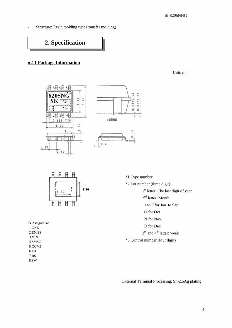
- Structure: Resin molding type (transfer molding)
●2-1 Package Information
2. Specification
External Terminal Processing: Sn-2.5Ag plating
Unit: mm
PIN Assignment
1.GND
2.EN/SS
3.VIN
4.SYNC
5.COMP
6.FB
7.BS
8.SW
*1 Type number
*2 Lot number (three digit)
1st letter: The last digit of year
2nd
letter: Month
1 to 9 for Jan. to Sep.
O for Oct.
N for Nov.
D for Dec.
3rd
and 4th letter: week
*3 Control number (four digit)
SI-8205NHG
5
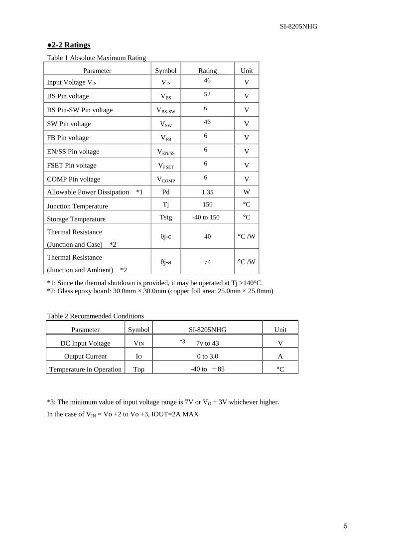
●2-2 Ratings
Table 1 Absolute Maximum Rating
Parameter Symbol Rating Unit
Input Voltage VIN VIN 46 V
BS Pin voltage VBS 52 V
BS Pin-SW Pin voltage VBS-SW 6 V
SW Pin voltage VSW 46 V
FB Pin voltage VFB 6 V
EN/SS Pin voltage VEN/SS 6 V
FSET Pin voltage VFSET 6 V
COMP Pin voltage VCOMP 6 V
Allowable Power Dissipation *1 Pd 1.35 W
Junction Temperature Tj 150 °C
Storage Temperature Tstg -40 to 150 °C
Thermal Resistance
(Junction and Case) *2
θj-c 40 °C /W
Thermal Resistance
(Junction and Ambient) *2
θj-a 74 °C /W
*1: Since the thermal shutdown is provided, it may be operated at Tj >140°C.
*2: Glass epoxy board: 30.0mm × 30.0mm (copper foil area: 25.0mm × 25.0mm)
Table 2 Recommended Conditions
Parameter Symbol SI-8205NHG Unit
DC Input Voltage VIN 7v to 43 V
Output Current IO 0 to 3.0 A
Temperature in Operation Top -40 to +85 °C
*3: The minimum value of input voltage range is 7V or VO + 3V whichever higher.
In the case of VIN = Vo +2 to Vo +3, IOUT=2A MAX
*3
SI-8205NHG
6
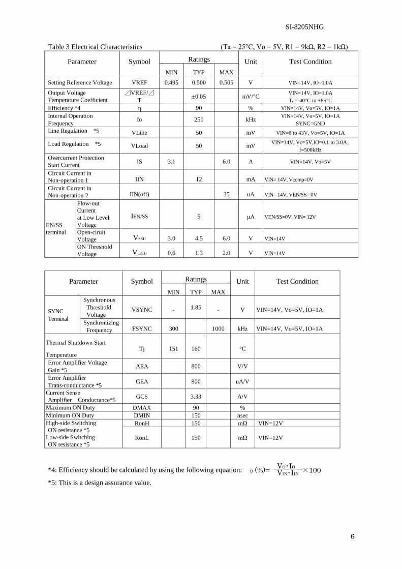
Table 3 Electrical Characteristics (Ta = 25°C, Vo = 5V, R1 = 9kΩ, R2 = 1kΩ)
Parameter Symbol Ratings Unit Test Condition
MIN TYP MAX
Setting Reference Voltage VREF 0.495 0.500 0.505 V VIN=14V, IO=1.0A
Output Voltage
Temperature Coefficient
⊿VREF/⊿T
±0.05 mV/°C VIN=14V, IO=1.0A
Ta=-40°C to +85°C
Efficiency *4 η 90 % VIN=14V, Vo=5V, IO=1A
Internal Operation
Frequency fo 250 kHz
VIN=14V, Vo=5V, IO=1A
SYNC=GND
Line Regulation *5 VLine 50 mV VIN=8 to 43V, Vo=5V, IO=1A
Load Regulation *5 VLoad 50 mV VIN=14V, Vo=5V,IO=0.1 to 3.0A ,
f=500kHz
Overcurrent Protection
Start Current IS 3.1 6.0 A VIN=14V, Vo=5V
Circuit Current in
Non-operation 1 IIN 12 mA VIN= 14V, Vcomp=0V
Circuit Current in
Non-operation 2 IIN(off) 35 uA VIN= 14V, VEN/SS= 0V
EN/SS
terminal
Flow-out
Current
at Low Level
Voltage
IEN/SS 5 μA VEN/SS=0V, VIN= 12V
Open-ciruit
Voltage VSSH 3.0 4.5 6.0 V VIN=14V
ON Threshold
Voltage VC/EH 0.6 1.3 2.0 V VIN=14V
Parameter Symbol Ratings Unit Test Condition
MIN TYP MAX
SYNC
Terminal
Synchronous
Threshold
Voltage VSYNC - 1.85 - V VIN=14V, Vo=5V, IO=1A
Synchronizing
Frequency FSYNC 300 1000 kHz VIN=14V, Vo=5V, IO=1A
Thermal Shutdown Start
Temperature Tj 151 160 °C
Error Amplifier Voltage
Gain *5 AEA 800 V/V
Error Amplifier
Trans-conductance *5 GEA 800 uA/V
Current Sense
Amplifier Conductance*5 GCS 3.33 A/V
Maximum ON Duty DMAX 90 %
Minimum ON Duty DMIN 150 nsec
High-side Switching
ON resistance *5
Low-side Switching
ON resistance *5
RonH 150 mΩ VIN=12V
RonL 150 mΩ VIN=12V
*4: Efficiency should be calculated by using the following equation:
*5: This is a design assurance value.
η(%)= ×100 VO・IO VIN・IIN
SI-8205NHG
7
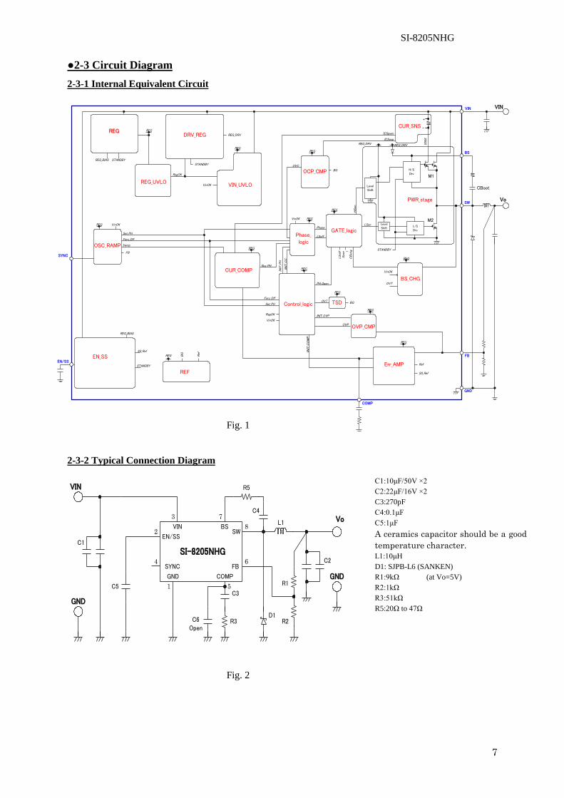
●2-3 Circuit Diagram
2-3-1 Internal Equivalent Circuit
Fig. 1
2-3-2 Typical Connection Diagram
Fig. 2
SYNC
EN/SS
BS
SW
GND
FB
COMP
VIN
Vo
VIN
REG_DRV
CBoot
REG
Ref
BG
REG
OVC
HSon
Phase
Res_PH
PH_OpenINIT_PH
REG
OVP
ICSocp
ICSpwm
INIT_COMP
REG
Iramp
REG
Set_PH
Forc_Off
SS_Ref
Phase_logic
CBchg
REG
REG
REG
FB
STANDBY
STANDBY
RegOK
REG_DRV
STANDBY
REG_UVLO
DRV_REG
Ref
BG
REG
REF
REG
VinOK
REG
CUR_COMP
SS_Ref
Err_AMP
RegOK
VinOK
VIN_UVLO
STANDBY
ISNS
CUR_SNS
OCP_CMP
OVP_CMP
REG
OVT BGTSD
INIT_OVP
Control_logic
LSoff
VinOK
OSC_RAMP
Szse l
PWR_stage
GATE_logic
REG_BIAS
REG
REG_BIAS
EN_SS
REG_DRV
LSon LevelShift
LevelShift
M1
M2L/SDrv
H/SDrv
REG
BS_CHGOVT
VinOK
LSoff
Forc_Off
Set_PH
INIT_CC
VinOK
Vo
C1
C3
D1
C4
L1
C2
R2
C5
R3
GND
GND
R1
SI-8205NHG
VIN BSSW
SYNC
GND COMP
FB
EN/SS
7
8
1
2
3
4
5
6
VIN R5
C6Open
C1:10μF/50V ×2
C2:22μF/16V ×2
C3:270pF
C4:0.1μF
C5:1μF
A ceramics capacitor should be a good
temperature character.
L1:10μH
D1: SJPB-L6 (SANKEN)
R1:9kΩ (at Vo=5V)
R2:1kΩ
R3:51kΩ
R5:20Ω to 47Ω
SI-8205NHG
8
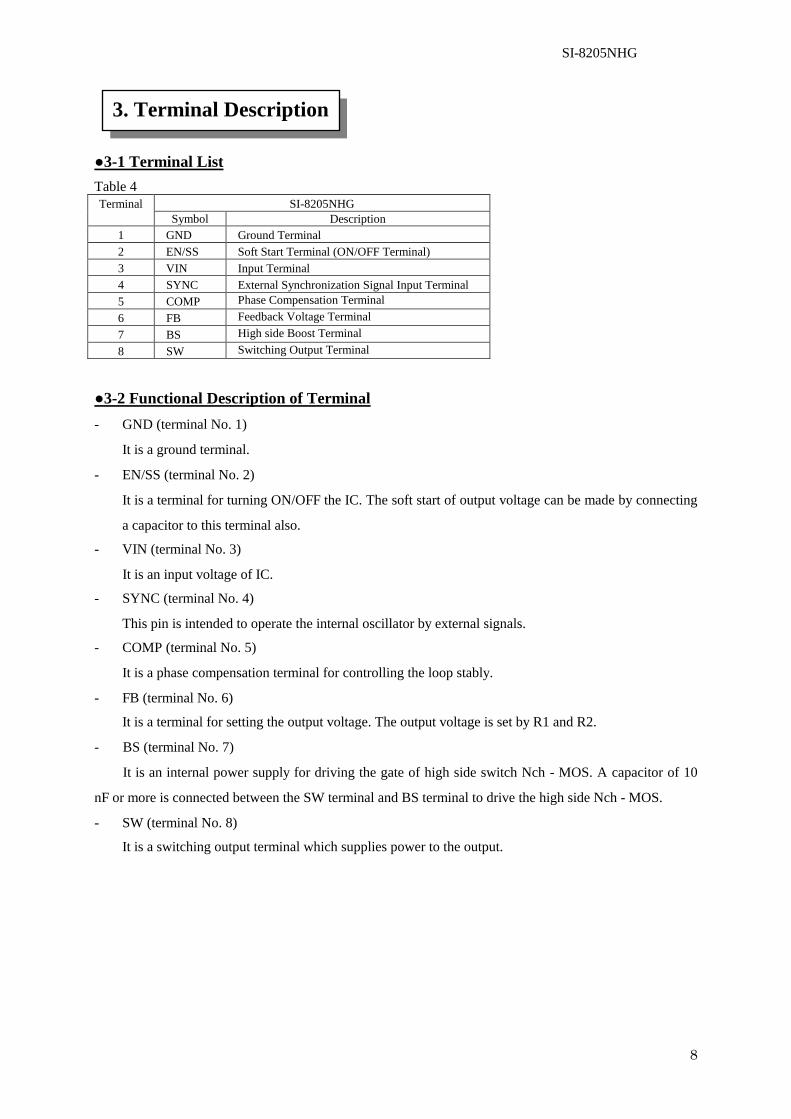
●3-1 Terminal List
Table 4
Terminal SI-8205NHG
Symbol Description
1 GND Ground Terminal
2 EN/SS Soft Start Terminal (ON/OFF Terminal)
3 VIN Input Terminal
4 SYNC External Synchronization Signal Input Terminal
5 COMP Phase Compensation Terminal
6 FB Feedback Voltage Terminal
7 BS High side Boost Terminal
8 SW Switching Output Terminal
●3-2 Functional Description of Terminal
- GND (terminal No. 1)
It is a ground terminal.
- EN/SS (terminal No. 2)
It is a terminal for turning ON/OFF the IC. The soft start of output voltage can be made by connecting
a capacitor to this terminal also.
- VIN (terminal No. 3)
It is an input voltage of IC.
- SYNC (terminal No. 4)
This pin is intended to operate the internal oscillator by external signals.
- COMP (terminal No. 5)
It is a phase compensation terminal for controlling the loop stably.
- FB (terminal No. 6)
It is a terminal for setting the output voltage. The output voltage is set by R1 and R2.
- BS (terminal No. 7)
It is an internal power supply for driving the gate of high side switch Nch - MOS. A capacitor of 10
nF or more is connected between the SW terminal and BS terminal to drive the high side Nch - MOS.
- SW (terminal No. 8)
It is a switching output terminal which supplies power to the output.
3. Terminal Description

SI-8205NHG
9
●4-1 PWM Output Voltage Control
The SI-8205NHG consists of two systems of feedback loops of current control and voltage control and
three blocks which compensate slope and, in the voltage control feedback, the output voltage is fed back
for PWM control loop and the SI-8205NHG is composed of an error amplifier which compares the division
of resistance with the reference voltage of 0.5V. The current control feedback is a loop which feeds back
the inductor current for PWM control and the inductor current shunted by using a sense MOS is detected
by a current sense amplifier. With respect to the slope compensation, in consideration of current control
system, in order to avoid the sub harmonic oscillation, slope compensation is made for the current control
slope. As shown in Fig.5, in the SI-8205NHG, by means of voltage control feedback, current control
feedback and calculation of slope compensation, the PWM control by current control system is made.
Since the SI-8205NHG is a current control regulator, the COMP terminal voltage is proportional to the
peak value of the inductor current. When the ULVO is released or current of the EN/SS terminal exceeds
the threshold value, the switching operation is made. At first, switching operation is made by MIN ON duty
or MAX ON duty. The high side switch (hereinafter called as M1) is a switching MOS which supplies
power to the output and a switch for charging the BS capacitor (hereinafter called as BS M) charges the
capacitor C4 to drive M1.
At M1: ON, inductor current is increased by applying voltage to the SW switch and inductor, and the
output of the current detection amplifier which detects it also rises. The signal to which the output of this
current detection amplifier and the Ramp compensation signal are added is compared with the output of the
error amplifier by the current comparator (CUR COMP). When the added signal exceeds the output of the
error amplifier (COMP terminal voltage), the output of the current comparator becomes “H” to reset the RS
flip-flop. Then, M1 turns off and M2 turns on. Thereby, the regenerated current flows through M2 and the
external SBD (D1).
In the SI-8205NHG, the reset signal is generated at each cycle to reset the RS flip-flop. In the case the
4. Operational Description
Fig.3 Current Control PWM Chopper Regulator Basic Configuration
M1
M2 BS_M
Reference Voltage 0.5V
SI-8205NHG
10
added signal does not exceed the COMP terminal voltage, the RS flip-flop is reset without fail by the signal
of the 10% OFF Duty circuit.
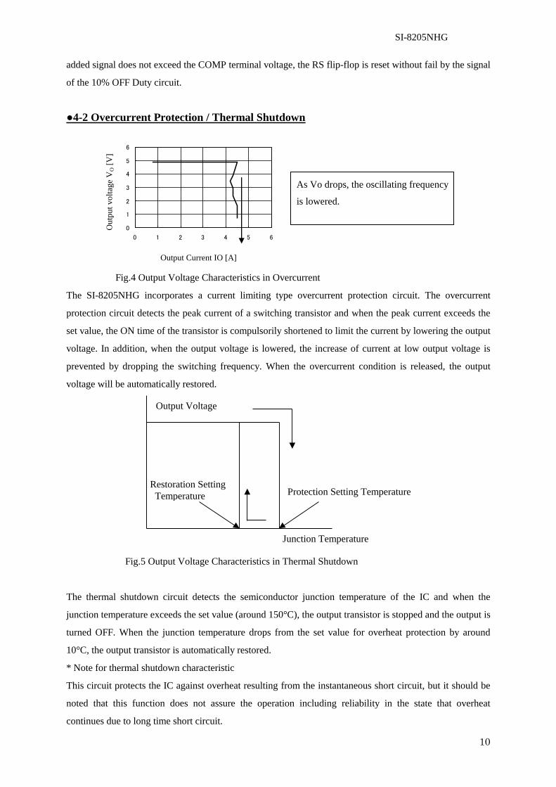
●4-2 Overcurrent Protection / Thermal Shutdown
Fig.4 Output Voltage Characteristics in Overcurrent
The SI-8205NHG incorporates a current limiting type overcurrent protection circuit. The overcurrent
protection circuit detects the peak current of a switching transistor and when the peak current exceeds the
set value, the ON time of the transistor is compulsorily shortened to limit the current by lowering the output
voltage. In addition, when the output voltage is lowered, the increase of current at low output voltage is
prevented by dropping the switching frequency. When the overcurrent condition is released, the output
voltage will be automatically restored.
Fig.5 Output Voltage Characteristics in Thermal Shutdown
The thermal shutdown circuit detects the semiconductor junction temperature of the IC and when the
junction temperature exceeds the set value (around 150°C), the output transistor is stopped and the output is
turned OFF. When the junction temperature drops from the set value for overheat protection by around
10°C, the output transistor is automatically restored.
* Note for thermal shutdown characteristic
This circuit protects the IC against overheat resulting from the instantaneous short circuit, but it should be
noted that this function does not assure the operation including reliability in the state that overheat
continues due to long time short circuit.
過電流保護特性
0
1
2
3
4
5
6
0 1 2 3 4 5 6
出力電流 I o[A]
出力
電圧
Vo[V]
出力電圧
接合温度
復帰設定温度 保護設定温度
As Vo drops, the oscillating frequency
is lowered.
Ou
tpu
t v
olt
age
VO [
V]
Output Current IO [A]
Junction Temperature
Protection Setting Temperature Restoration Setting
Temperature
Output Voltage

SI-8205NHG
11
●5-1 External Components
5-1-1 Choke coil L1
The choke coil L1 plays a main role in the chopper type switching regulator. In order to maintain the stable
operation of the regulator, such dangerous state of operation as saturation state and operation at high
temperature due to heat generation must be avoided.
The following points should be taken into consideration for the selection of the choke coil.
a) The choke coil should be fit for the switching regulator.
The coil for a noise filter should not be used because of large loss and generated heat.
b) For the peak detection current control, the inductance current may fluctuate at the cycle of integral
multiple of switching operation frequency.
Such phenomenon is called as sub harmonic oscillation and it may theoretically occur in the peak detection
current control mode.
Therefore, in order to assure stable operation, the inductance current is compensated inside the IC, and it is
required to select a proper inductance value to the output voltage.
Fig. 6 shows the selection range of the inductance L value to avoid the sub harmonic oscillation. The upper
limit of inductance L is variable subject to the input/output conditions, load current etc., therefore please
regard it as a reference in the Fig. 6 below.
Fig. 6 Selection range of the inductance L value
5. Cautions
Inductance L
Selectable area
Output Voltage Vo [V]
Induct
ance
L [
μH
]
SI-8205NHG
12
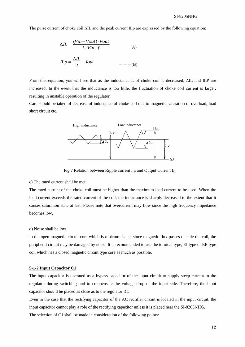
The pulse current of choke coil ΔIL and the peak current ILp are expressed by the following equation:
From this equation, you will see that as the inductance L of choke coil is decreased, ΔIL and ILP are
increased. In the event that the inductance is too little, the fluctuation of choke coil current is larger,
resulting in unstable operation of the regulator.
Care should be taken of decrease of inductance of choke coil due to magnetic saturation of overload, load
short circuit etc.
Fig.7 Relation between Ripple current ILP and Output Current IO
c) The rated current shall be met.
The rated current of the choke coil must be higher than the maximum load current to be used. When the
load current exceeds the rated current of the coil, the inductance is sharply decreased to the extent that it
causes saturation state at last. Please note that overcurrent may flow since the high frequency impedance
becomes low.
d) Noise shall be low.
In the open magnetic circuit core which is of drum shape, since magnetic flux passes outside the coil, the
peripheral circuit may be damaged by noise. It is recommended to use the toroidal type, EI type or EE type
coil which has a closed magnetic circuit type core as much as possible.
5-1-2 Input Capacitor C1
The input capacitor is operated as a bypass capacitor of the input circuit to supply steep current to the
regulator during switching and to compensate the voltage drop of the input side. Therefore, the input
capacitor should be placed as close as to the regulator IC.
Even in the case that the rectifying capacitor of the AC rectifier circuit is located in the input circuit, the
input capacitor cannot play a role of the rectifying capacitor unless it is placed near the SI-8205NHG.
The selection of C1 shall be made in consideration of the following points:
fVinL
VoutVoutVinIL
)(
IoutIL
ILp
2
---(A)
---(B)
High inductance Low inductance

SI-8205NHG
13
a) The requirement of withstand voltage shall be met.
b) The requirement of the allowable ripple voltage shall be met.
Fig.8 Current Flow of C1 Fig. 9 Current Waveform of C1
If the withstanding voltages or allowable ripple voltages are exceeded or used without derating, it is in
danger of causing not only the decreasing the capacitor lifetime (burst, capacitance decrease, equivalent
impedance increase, etc) but also the abnormal oscillations of regulator.
Therefore, the selection with sufficient margin is needed.
The effective value of ripple current flowing across the input capacitor can be obtained by the following
equation (2):
IoVin
VoIrms 2.1 --(2)
For instance, where VIN=20V, Io=3A, Vo=5V
AI r m s 9.0320
52.1
Therefore, it is necessary to select the capacitor with the allowable ripple current of 0.9A or higher.
5-1-3 Output Capacitor C2
The current control system is a voltage control system to which a loop which detects and feeds back the
inductance current is added. By adding inductor current to the feedback loop, stable operation is realized
without taking into consideration the influence of secondary delay of the LC filter. Therefore, the
capacitance C of the LC filter which is required to compensate the secondary delay can be decreased and
furthermore, stable operation can be obtained, even if the low ESR capacitor (ceramic capacitor) is used.
The output capacitor C2 composes a LC low pass filter together with a choke coil L1 and functions as a
rectifying capacitor of switching output.
The current equivalent to the pulse current ΔIL of the choke coil current is charged and discharged in the
C1
1.VIN
IIN
VIN
リップル電流 IvIp
Ton
T
0
C1電流波形
The ripple current of the input capacitor
is increased in accordance with the
increase of the load current.
T
TonD
Ripple Current

SI-8205NHG
14
output capacitor.
Therefore, it is necessary to meet the requirements of withstand voltage and allowable ripple current with
sufficient margin like the input capacitor.
Fig.10 C2 current flow Fig.11 C2 current curve
The ripple current effective value of the output capacitor is obtained by the equation (3).
IrmsIL
2 3 ---(3)
When ΔIL = 0.5A,
Irms A05
2 3014
..≒
Therefore a capacitor having the allowable ripple current of 0.14A or higher is required.
In addition, the output ripple voltage Vrip of the regulator is determined by a product of the pulse current
ΔIL of the choke coil current (= C2 charging/discharging current) and the equivalent series resistance ESR
of the output capacitor.
Vrip IL C ESR 2 ---(4)
It is therefore necessary to select a capacitor with low equivalent series resistance ESR in order to lower the
output ripple voltage. As for general electrolytic capacitors of same product series, the ESR shall be lower,
for the products of higher capacitance with same withstand voltage, or with higher withstand voltage
(almost proportional to larger externals) with same capacitance.
When ΔIL=0.5A, Vrip=40mV,
C esr m2 40 05 80 .
As shown above, a capacitor with the ESR of 80mΩ or lower should be selected. In addition, since the ESR
varies with temperature and increases at low temperature, it is required to examine the ESR at the actual
operating temperatures. It is recommended to contact capacitor manufacturers for the ESR value since it is
peculiar to capacitors.
ESR
C2
Vout
Ioリップル電流
IL
L1
0 ⊿IL
C2電流波形
RL
The ripple current of the output capacitor is
equal to the ripple current of the choke coil and
does not vary even if the load current increases
or decreases.
Ripple current

SI-8205NHG
15
5-1-4 Flywheel Diode D1
The SI-8205NHG has a switch-over function between synchronous rectification and asynchronous one
subject to input/output conditions, load conditions etc.. Since asynchronous operation is made as well, it is
recommended to connect a fly wheel diode D1 externally.
The flywheel diode D1 is to discharge the energy which is stored in the choke coil at switching OFF.
For the flywheel diode, the Schottky barrier diode must be used. If a general rectifying diode or fast
recovery diode is used, the IC may be destroyed by applying reverse voltage due to the recovery and ON
voltage.
In addition, since the output voltage from the SW terminal (pin 8) of the SI-8205NHG series is almost
equivalent to the input voltage, the flywheel diode with the reverse withstand voltage of the input voltage or
higher should be used.
It is recommended not to use the ferrite bead for the flywheel diode.
5-1-5 Phase compensation elements C3, C6, R3
The stability and responsiveness of the loop are controlled through the COMP terminal.
The COMP terminal is an output of the internal trans-conductance amplifier.
The series combination of a capacitor and resistor sets the combination of pole and zero which determines
characteristics of the control system. The DC gain of voltage feedback loop can be calculated by the
following equation:
Here, VFB is feedback voltage (0.5V). AEA is the voltage gain of error amplifier, GCS trans-inductance of
current detection and R1 a load resistance value. There are two important poles. One is produced by a
phase compensation capacitor (C3) and an output resistor of the error amplifier.
Another one is produced by a output capacitor and a load resistor. These poles appear at the following
frequencies:
Here, GEA is the trans-conductance of error amplifier. In this system, one zero is important. This zero is
produced by phase compensation capacitor C3 and phase compensation resistance R3. This zero appears in
the following frequencies:
If the output capacitor is large and/or ESR is large, this system may have another important zero. This zero
is produced by the ESR and capacitance of the output capacitor. And it exists in the following frequencies:
Vout
VAGcs
FBEA RlAdc
EA
EA
AC
Gfp
321
RlCfp
22
12
332
11
RCfz
RESRCfESR
22
1

SI-8205NHG
16
In this case, the third pole which is set by the phase compensation capacitor (C6) and phase compensation
resistor (R3) is used to compensate the effect of ESR zero on the loop gain.
This pole exists in the following frequencies:
The objective of design of phase compensation is to form the converter transfer function to obtain the
desired loop gain. The system crossover frequency where the feedback loop has a single gain is important.
The lower crossover frequency will produce the slower line and load transient. In the meantime, the higher
crossover frequency may cause instability of the system. The selection of the most suitable phase
compensation element is described below.
1. A phase compensation resistor (R3) is selected to set the resistor at the desired crossover frequency.
The calculation of R3 is made by the following equation:
Here, fc is a desired crossover frequency. It should be one tenth or lower of the normal switching frequency
(fs).
2. In order to achieve the desired phase margin, a phase compensation capacitor (C3) is selected.
For the application having a representative inductance value, adequate phase margin is provided by setting
the zero compensation of one fourth or lower of the crossover frequency.
C3 is calculated by the following equation.
R3 is a phase compensation resistor.
3. It is required to judge whether the second compensation capacitor C6 is necessary or not.
It will be necessary, when the ESR zero of the output capacitor is located at a frequency which is lower
than the half of the switching frequency.
Namely, it is necessary, when the following equation is applicable.
In this case, the second compensation capacitor C6 is added and the frequency fp3 of ESR zero is set.
C6 is obtained from the following equation.
The constants for each output setting voltage in the case that ceramic capacitors or aluminum electrolytic
capacitors are used are shown in the following table.
The inductor L should be selected by reference to the choke coil L1 of 5-1-1. (Refer to Fig. 6 Scope of
362
13
RCfp
FBV
Vout
GCSGEA
fsC
VFB
Vout
GCSGEA
fcCR
1.022223
fcRC
32
43
222
1 fs
RESRC
3
26
R
RESRCC

SI-8205NHG
17
selection of inductance L value)
Table 5
Output
setting
voltage (use
ceramic
capacitors)
Table 6 Output setting voltage (use aluminum electrolytic capacitors)
Vout
[V]
L
[uH]
Cout[uF]
(ceramic capacitor)
fc=50kHz fc=20kHz
R3
[kΩ]
C3
[pF]
C6
[pF]
R3
[kΩ]
C3
[pF]
C6
[pF]
1.2 2.0 - 10 22 x 2 12 1000 No 4.7 6800 No
1.8 3.0 - 10 22 x 2 18 680 No 7.3 4700 No
3.3 6.8 - 16 22 x 2 33 330 No 13 3300 No
5 8.2 - 22 22 x 2 51 220 No 20 1800 No
12 22 - 68 22 x 2 124 100 No 47 680 No
Vout
[V]
L
[uH]
Cout [uF]/
ESR [mΩ]
(aluminum electrolytic capacitor)
fc=50kHz fc=20kHz
R3
[kΩ]
C3
[pF]
C6
[pF]
R3
[kΩ]
C3
[pF]
C6
[pF]
1.2 2.0 - 10 220/100 62 220 470 24 1500 1000
1.8 3.0 - 10 220/100 91 180 330 36 1000 680
3.3 6.8 - 16 220/100 160 100 180 68 470 330
5 8.2 - 22 220/100 240 100 100 100 330 220
12 22 - 68 220/100 620 100 100 240 150 100

SI-8205NHG
18
●5-2 Pattern Design Notes
5-2-1 High Current Line
Since high current flows in the bold lines in the connection diagram, the pattern should be as wide and
short as possible.
5-2-2 Input/ Output Capacitor
The input capacitor C1 and the output capacitor C2 should be placed to the IC as close as possible. If the
rectifying capacitor for AC rectifier circuit is on the input side, it can be used as an input capacitor.
However, if it is not close to the IC, the input capacitor should be connected in addition to the rectifying
capacitor. Since high current is discharged and charged through the leads of input/output capacitor at high
speed, the leads should be as short as possible. A similar care should be taken for the patterning of the
capacitor.
C1,C2 C1,C2
Fig. 13 Improper Pattern Example Fig. 14 Proper Pattern Example
SI-8205NHD
IN BSSW
SS/ENGNDCOMP
FB
R3
R2
R1
C4
C1
C2
C5C3
C6OPEN
L1
FEST
D1
VIN
VO
1
2
3
4
5
6
7
8
GND GND
VFB
IADJ
R4
Fig. 12 Circuit Diagram
SI-8205NHG
SYNC

SI-8205NHG
19
5-2-3 FB Terminal (Output Voltage Set-up)
The FB terminal is a feedback detection terminal for controlling the output voltage. It is recommended to
connect it as close as possible to the output capacitor C2. When they are not close, the abnormal oscillation
may be caused due to the poor regulation and increase of switching ripple. The output voltage set-up is
achieved by connecting R1 and R2. IFB should be set to be around 0.5mA.
(The IFB lower limit is 0.5mA, and the upper limit is not defined. However, it is necessary to consider that
the consumption current shall increase according to the IFB value, resulting in lower efficiency.)
R1, R2 and output voltage are calculated from the following equations:
IFB=VFB/R2 *VFB=0.5v±1%
R1=(Vo-VFB) / IFB R2=VFB / IFB
Vout=R1× (VFB/R2) +VFB
- R2 should be connected for the stable operation when set to Vo = 0.5V.
- As to the relationship with the input/output voltage, it is recommended to set the ON width of SW
terminal to be 200 nsec or longer.
The wiring of COMP terminal, FB terminal, R1 and R2 that run parallel to the flywheel diode should be
avoided, because switching noise may interfere with the detection voltage to cause abnormal oscillation. It
is recommended to implement the wiring from the FB terminal to R2 as short as possible.
Fig. 15
SI-8205NHG
20
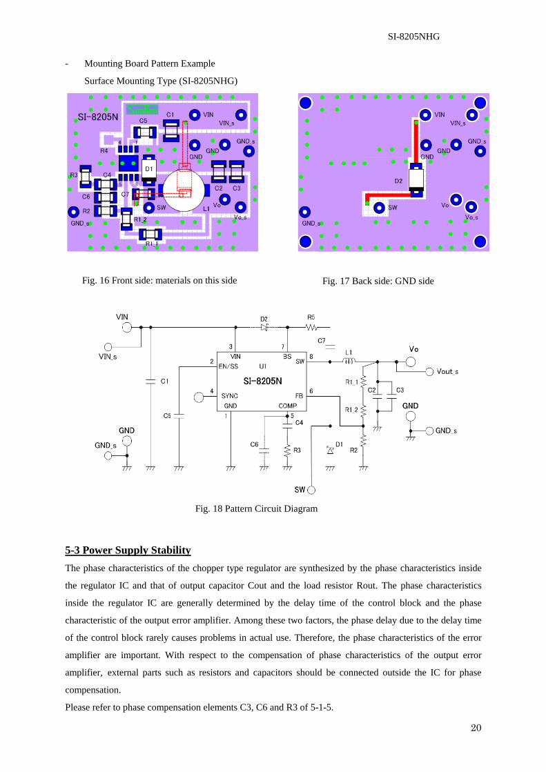
- Mounting Board Pattern Example
Surface Mounting Type (SI-8205NHG)
5-3 Power Supply Stability
The phase characteristics of the chopper type regulator are synthesized by the phase characteristics inside
the regulator IC and that of output capacitor Cout and the load resistor Rout. The phase characteristics
inside the regulator IC are generally determined by the delay time of the control block and the phase
characteristic of the output error amplifier. Among these two factors, the phase delay due to the delay time
of the control block rarely causes problems in actual use. Therefore, the phase characteristics of the error
amplifier are important. With respect to the compensation of phase characteristics of the output error
amplifier, external parts such as resistors and capacitors should be connected outside the IC for phase
compensation.
Please refer to phase compensation elements C3, C6 and R3 of 5-1-5.
Fig. 16 Front side: materials on this side Fig. 17 Back side: GND side
Fig. 18 Pattern Circuit Diagram

SI-8205NHG
21
●6-1 Soft Start
When a capacitor is connected to terminal 2, the soft start is activated when the input voltage is applied.
Vout rises in relation with the charging voltage of Css. Therefore, the rough estimation is done by the time
constant calculation of Css charging.
The capacitor Css controls the rise time by controlling the OFF period of PWM control. The rise time tss
and the delay time t_delay are obtained approximately by the following equation:
It is the delay time t_delay when voltage of EN/SS terminal <1.6V.
It is the rise time tss when 1.6V< voltage of EN/SS <2.1V
t_delay = CEN/SS × VEN/SS-1 / IEN/SS = 0.1μF × 1.6V / 5μA = 32msec
tss = CEN/SS × (VEN/SS-2 – VEN/SS-1) / IEN/SS = 0.1μF × 0.5V / 5μA = 10msec
When not using the soft start function, the No.2 terminal should be open.
Since the EN/SS terminal is pulled up (4.5V TYP) with the internal power supply of IC, the external
voltage can not be applied.
If there is no Css or it is extremely low, Vout rises at the time constants charging the output capacitor with
the output current restricted by the overcurrent protection Is.
Time constants at output capacitor start-up
t = (Co × Vo) / Is (at no load)
6. Applications
Fig. 19 Characteristic on Soft Start
SI-8205NHG
22
*The amount of load current is deducted from the Is value at load.
●6-2 Output ON / OFF Control
The output ON-Off control is possible using the EN/SS terminal (No.2). The output is turned OFF when
the terminal 5 voltage falls below VC/EH (1.6V TYP) by such as open collector. It is possible to use the soft
start together. Since the soft start terminal has been already pulled up (4.5V TYP), no voltage shall be
applied from the external side.
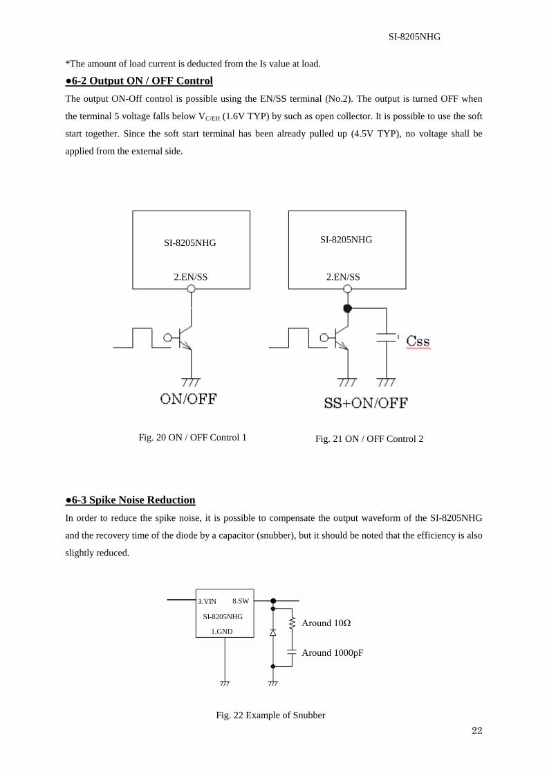
●6-3 Spike Noise Reduction
In order to reduce the spike noise, it is possible to compensate the output waveform of the SI-8205NHG
and the recovery time of the diode by a capacitor (snubber), but it should be noted that the efficiency is also
slightly reduced.
SI-8205NHG SI-8205NHG
2.EN/SS 2.EN/SS
SI-8205NHG
1.GND
3.VIN 8.SW
Fig. 20 ON / OFF Control 1 Fig. 21 ON / OFF Control 2
Fig. 22 Example of Snubber
Around 10Ω
Around 1000pF

SI-8205NHG
23
* When the spike noise is observed with an oscilloscope, the lead wire may function as an antenna and the
spike noise may be observed extremely higher than usual if the probe GND lead wire is too long. In the
observation of spike noise, the probe lead wire should be as short as possible and be connected with the
root of the output capacitor.
●6-4 Reverse Bias Protection
A diode for reverse bias protection will be required between input and output when the output voltage is
higher than the input terminal voltage, such as in battery chargers.
●6-5 External synchronization
When the external signal is input (300kHz (TYP) to 1MHz (TYP)) to the 4th pin, operation can be
performed at a frequency in synchronization with external signals. Fig.24 shows the operating waveform in
synchronization with external signals. In addition, the operation is performed at a fixed frequency 250kHz
by connecting the 4th pin to GND.
SI-8205NHD3PIN 8PIN
Fig. 23 Diode for Reverse Bias Protection
Fig.24 External synchronization operation
SI-8205NHG
Condition
External synchronization 500 kHz (2 μsec/ div) External synchronization 1 MHz (1 μsec/ div)
SYNC terminal (external input: 500 kHz) SYNC terminal (external input: 1 MHz)
SW terminal (operation frequency) SW terminal (operation frequency)

SI-8205NHG
24
- Jitter
It is a kind of abnormal switching operations and is a phenomenon that the switching pulse width varies in
spite of the constant condition of input and output. The output ripple voltage peak width is increased when
a jitter occurs.
- Recommended Conditions
It shows the operation conditions required for maintaining normal circuit functions. It is required to meet
the conditions in actual operations.
- Absolute Maximum Ratings
It shows the destruction limits. It is required to take care so that even one item does not exceed the
specified value for a moment during instantaneous or normal operation.
- Electrical Characteristics
It is the specified characteristic value in the operation under the conditions shown in each item. If the
operating conditions are different, it may be out of the specifications.
- PWM (Pulse Width Modulation)
It is a kind of pulse modulation systems. The modulation is achieved by changing the pulse width in
accordance with the variation of modulation signal waveform (the output voltage for chopper type
switching regulator).
- ESR (Equivalent Series Resistance)
It is the equivalent series resistance of a capacitor. It acts in a similar manner to the resistor
series-connected to the capacitor.
7. Terminology

SI-8205NHG
25
Notice
・The contents of this description are subject to change without prior notice for improvement etc. Please
make sure that any information to be used is the latest one.
・Any example of operation or circuitry described in this application note is only for reference, and we are
not liable to any infringement of industrial property rights, intellectual property rights or any other rights
owned by third parties resulting from such examples.
・In the event that you use any product described here in combination with other products, please review the
feasibility of combination at your responsibility.
・Although we endeavor to improve the quality and reliability of our product, in the case of semi-conductor
components, defects or failures which occur at a certain rate of probability are inevitable.
The user should take into adequate consideration the safety design in the equipment or the system in order to
prevent accidents causing death or injury, fires, social harms etc..
・Products described here are designed to be used in the general-purpose electronic equipment (home
appliances, office equipment, communication terminals, measuring equipment etc.).
If used in the equipment or system requiring super-high reliability (transport machinery and its control
equipment, traffic signal control equipment, disaster/crime prevention system, various safety apparatus etc.),
please consult with our sales office. Please do not use our product for the equipment requiring ultrahigh
reliability (aerospace equipment, atomic control, medical equipment for life support etc.) without our written
consent.
・The products described here are not of radiation proof type.
・The contents of this brochure shall not be transcribed nor copied without our written consent.