supporting information - rsc.org · supporting information non-volatile transistor memory devices...
TRANSCRIPT

Supporting Information
Non-volatile Transistor Memory Devices using Charge Storage Cross-
Linked Core-Shell Nanoparticles
Chen-Tsyr Loa, Yu Watanabeb, Hiroshi Oyab, Kazuhiro Nakabayashib, Hideharu Morib,*
Wen-Chang Chena,*
a Department of Chemical Engineering, National Taiwan University, Taipei, Taiwan
b Department of Polymer Science and Engineering, Graduate School of Science and
Engineering, Yamagata University, Yonezawa, Japan
*To whom all correspondence should be addressed.
E-mail: W. C. Chen ([email protected]); H. Mori ([email protected])
Electronic Supplementary Material (ESI) for ChemComm.This journal is © The Royal Society of Chemistry 2016
Experimental
Materials
Poly(PEGMA) (Mn ~ 38000 and 17000 g mol-1) and the block copolymer
poly(PEGMA)m-b-poly(DB3VT)n were prepared through two-step RAFT polymerization
according to our previous report.33 The information of synthesis is simply tabulated both in
Table 1 and Table S1 of the Supporting Information (SI). The molecular weights of
poly(DB3VT) segment in the two block copolymers were adjusted to be almost the same (Mn
~ 4000 g mol-1), whereas the chain length of the hydrophilic poly(PEGMA) segment and
comonomer composition were different. Poly(DB3VT) (Mn ~ 9000 g mol-1) was also
prepared for comparison with those of block copolymers. Subsequently, the cross-linked
core-shell poly(PEGMA)m-b-poly(DB3VT)n nanoparticles with two different m:n ratios of
90:10 (P1) and 77:23 (P2) were synthesized through Suzuki coupling reaction as we
previously reported.33 Pentacene was purchased from Luminescence Technology corp.
(Hsinchiu, Taiwan). Other chemicals were used as received unless otherwise stated.
Synthesis of poly(DB3VT) by RAFT polymerization
Poly(DB3VT) homopolymer was prepared by following the reaction scheme illustrated
in Scheme S3, 2,5-Dibromo-3-vinylthiophene (0.67 g, 2.5 mmol), cumyl dithiobenzoate as
the chain transfer agent (CTA, 6.8 mg, 0.025 mmol), AIBN (0.82 mg, 0.005 mmol), and dry
1,4-dioxane (1.3 mL) were placed in a dry glass ampule equipped with a magnetic stir bar,
and then the solution was degassed by three freeze-evacuate-thaw cycles. After flame-sealed
under vacuum, the ampule was stirred at 60 °C for 24 h in the dark. The reaction was stopped
by rapid cooling with liquid nitrogen, and the reaction mixture was then precipitated in a
large excess of n-hexane and isolated by filtration. The resulting product was finally dried
under vacuum at room temperature to yield a pale red powder (160 mg, 24%). 1H NMR
(CDCl3, δ, ppm): 6.22-6.72 (m, 1H), 2.03-2.72 (m, 1H), 1.11-1.89 (m, 2H). Mn and Mw/Mn
calculated by GPC (THF) were 3700 and 1.03 g mol-1, respectively. The 1H NMR spectrum
is shown in Figure S1 (Supporting Information, SI), in which the characteristic peak
corresponding to DB3VT unit is clearly recognized at 6.3 to 6.7 ppm. The molecular weight
calculated by 1H NMR was 9000 g mol-1.
Synthesis of Poly(PEGMA)m-b-Poly(DB3VT)n
A two-step RAFT polymerization, first introduced by our previous work,32,33 was carried
out for preparing the amphiphilic block copolymers composed of PEGMA and DB3VT,
poly(PEGMA)-b-poly(DB3VT). The details of synthesis are tabulated in both Table 1 and

Table S1(Supporting Information, SI), where the synthetic route was provided in Scheme S1.
In the first step, poly(PEGMA) with two different values of molecular weight were prepared
from PEGMA using cumyl dithiobenzoate as CTA: Mn,NMR = 38 000 (Mw/Mn = 1.26) and 17
000 (Mw/Mn = 1.11) g mol-1. In the second step, poly(PEGMA)m-b-poly(DB3VT)n with two
block compositions (m:n = 90:10 and 77:23) were synthesized by RAFT polymerization of
DB3VT using two poly(PEGMA) as macro-CTA under suitable conditions, respectively.
According to our previous study, the block compositions (m:n) of each segment in the block
copolymers can be precisely controlled by adjusting the [M]:[macro-CTA] ratios.33 While the
ratio of [macro-CTA]:[AIBN] was maintained as 5:1, the polymerization was thus carried out
at 60 °C for 24 h with different ratios of [M]:[macro-CTA], 140:1 and 30:1, and resulted in
the block copolymers, poly(PEGMA)m-b-poly(DB3VT)n, with two different m:n ratios, i.e.
90:10 and 77:23, respectively. For the synthesis of block copolymer with77:23 molar ratio,
poly(PEGMA) macro-CTA (0.45 g, 0.026 mmol, Mn,NMR = 17000), DB3VT (0.211 g, 0.79
mmol), AIBN (0.86 mg, 0.005 mmol), and dry 1,4-dioxane (0.79 mL) were placed in a dry
glass ampule equipped with a magnetic stir bar. After the solution was degassed using three
freeze-evacuate-thaw cycles, the reaction was carried out at 60 oC for 24 h with stirring. The
reaction mixture was poured into hexane, and then the precipitate was collected with
decantation and dried in vacuo at room temperature to yield light red viscous product (60%,
0.398 g). The compositions of each segment (m:n) was evaluated using by comparison of the
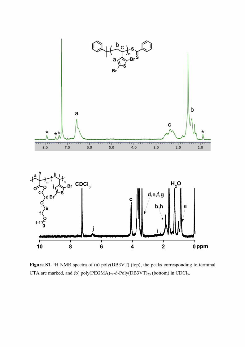
area of the peak at 6.2-6.7 ppm attributed to the heterocyclic proton (1H) of DB3VT unit and
3.9-4.2 ppm corresponding to the methylene protons (2H) of poly(PEGMA) unit (Figure S1,
SI). Herein, DB3VT was successfully polymerized from the dithiobenzoate-terminated
macro-CTA to yield amphiphilic block copolymers with narrow polydispersities (Mw/Mn =
1.26 to 1.43).
Preparation of Cross-Linked Nanoparticles
Following by the Suzuki coupling reaction (Scheme S2),33 the cross-linked nanoparticles
with different m:n ratios was respectively carried out using the poly(PEGMA)m-b-
poly(DB3VT)n and 2,5-thiophenediboronic acids in a THF/H2O solution in the presence of
the catalytic amount of Pd(dppf)Cl2 at 70 °C for 24 h. Considering the solvent is a dominant
factor in the preparation of well-defined nanoparticles,33 the volume ratio of the THF/H2O
solution was fixed as 3:7 vol %, in which the poly(PEGMA)-b-poly(DB3VT) can form well-
defined micelles consisting of a hydrophobic core of poly(DB3VT) covered with a
hydrophilic shell of poly(PEGMA) segments. The inter- and intra-molecular coupling
reaction to form polythiophene segments within micelles thus led to the formation of cross-
linked core-shell nanoparticles under the Suzuki coupling reaction. A typical procedure (P2
in Table 1) is as follows; The THF solution (15 mL) of poly(PEGMA)77-b-poly(DB3VT)23
(48 mg, 0.2 mmol based on the repeating unit), 2,5-thiophenedibronic acid (0.172 g, 1.0
mmol), NaHCO3 (0.34 g, 4.0 mmol) was stirred at room temperature under argon atmosphere.
After the block copolymer was completely dissolved, Pd(dppf)Cl2 (16.3 mg, 0.02 mmol) and
water (35 mL) was added, and the reaction mixture was carried out at 70 oC for 24 h in the
dark. Thereafter, dialysis in sequence with water and then with THF was employed to yield
brown viscous product (85%, 48 mg). The products are soluble in common organic solvent,
such as THF, chloroform, and dichloromethane regardless of the block composition.
Device fabrication
The pentacene-based transistor-type memory devices were fabricated on the wafer with a
thermally grown 100-nm-thick SiO2 dielectric on highly doped n-type Si as gate electrode.
The solutions of poly(PEGMA), poly(DB3VT), and cross-linked poly(PEGMA)m-b-
poly(DB3VT)n nanoparticles with the concentration of 3 mg mL-1 in chloroform was
respectively spin-coated at 1000 rpm for 60 s on wafers. Prior to the spin-coating process, the
polymer solutions were filtered using Millipore Teflon Filters with a pore size of 0.2 μm into
a dust-free cylindrical cuvette and the substrates were rinsed with toluene, acetone, and IPA
in sequence. Thereafter, the polymer thin films were dried under vacuum (10-6 torr) at room
temperature for 6 h to remove residual solvents. Thin films were thus prepared on the SiO2/Si
substrates for OFET memory devices as well as for the following characterizations. The
thickness of the prepared thin film was estimated to be around 50 nm. A 50-nm-thick
pentacene active layer was prepared by thermal deposition with a rate of 0.5 Å s-1 under 90
°C and 5 × 10⁻⁷ torr. The top-contact source and drain electrodes were defined by 80-nm-
thick gold through a regular shadow mask and the channel length (L) and width (W) were 50
and 1000 μm, respectively. The current-voltage (I−V) characteristics of the devices measured using a Keithley 4200-SCS semiconductor parameter analyzer in a N2-filled glove box. Ids =
μ(WC/2L)(Vgs−Vt)2, where Ids is the source–drain current, Vgs and Vt gate and threshold
voltage, respectively, C the capacitance of the device, W and L the channel width and length.
Characterization1H NMR (400 MHz) spectrum was recorded JEOL JNM-ECX400. The UV-vis spectra
were recorded with a on a JASCO V-630BIO UV-vis spectrophotometer. The thickness of
the thin film prepared for UV-vis analysis was estimated to be around 50 nm. Fluorescence
spectra were obtained from a JASCO FP-6100 spectrofluorophotometer. Number-average

molecular weight (Mn) and molecular weight distribution (Mw/Mn) were estimated by GPC
using a system consisting of a Tosoh DP-8020 pump and Viscotek. The column set was as
follows: a guard column [TSK guard column HXL-H (4.0 cm) and four consecutive columns
(Tosoh TSK-GELs (exclusion limited molecular weight): GMHXL (4 × 10⁸), G4000HXL (4
× 105), G3000HXL (6 × 10⁴), and G2500HXL (2 × 10⁴), 30 cm each) eluted with THF at a
flow rate of 1.0 mL/min, where polystyrene standards were employed for calibration. DLS
measurement was performed by using a Sysmex Zatasizwer Nano with a He−Ne laser (λ0 =
632.8 nm) and a scattering angle of 90°. Prior to the light scattering measurement, the
polymer solutions were filtered using Millipore Teflon Filters with a pore size of 0.2 μm into
a dust-free cylindrical cuvette.
The thickness of polymer films was measured with a microfigure measuring instrument
(Surfcorder ET 3000, Kosaka Laboratory Ltd.). The thin-film samples for morphology
analysis were prepared from the same condition with device fabrication, which are
respectively spin-coated from the solutions with of 3.0 mg mL-1 in chloroform. Atomic force
microscopy (AFM) measurement was performed with a NanoScope IIIa AFM (Digital
Instrument) at room temperature, where the commercial silicon cantilevers with typical
spring constraints of 21−78 N m-1 was employed to operate the AFM in tapping mode.
Transmission electron microscope (TEM) images were obtained using a JOEL JEM-1230
operated at 100 kV, equipped with a Gatan Dual Vision CCD. The samples for TEM
characterization were prepared by spin-coating at 1000 rpm for 60 s onto the carbon-coated
copper grids. Note that the surface energies of carbon (62 mJ m-2) and SiO2 (54 mJ m-2) are
similar, and thus carbon-coated grids are generally regarded as reliable substrate to simulate
the morphology on the SiO2/Si surface. For the capacitance analysis, a metal-insulator-
semiconductor (MIS) capacitor was fabricated by depositing gold electrodes on the polymer-
coated n-type Si(100) wafers. The capacitance of the bilayer dielectrics was measured on the
MIS structure using Keithley 4200-SCS equipped with a digital capacitance meter (model
4210-CVU).
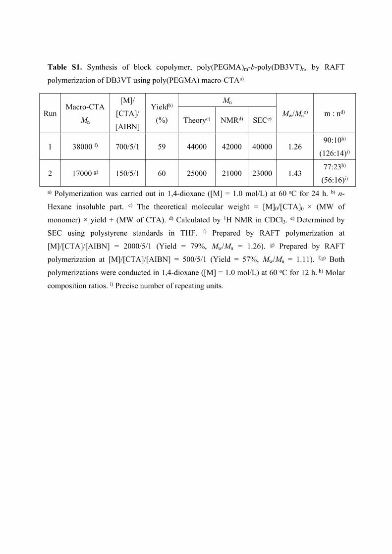
Table S1. Synthesis of block copolymer, poly(PEGMA)m-b-poly(DB3VT)n, by RAFT
polymerization of DB3VT using poly(PEGMA) macro-CTAa)
a) Polymerization was carried out in 1,4-dioxane ([M] = 1.0 mol/L) at 60 oC for 24 h. b) n-
Hexane insoluble part. c) The theoretical molecular weight = [M]0/[CTA]0 × (MW of
monomer) × yield + (MW of CTA). d) Calculated by 1H NMR in CDCl3. e) Determined by
SEC using polystyrene standards in THF. f) Prepared by RAFT polymerization at
[M]/[CTA]/[AIBN] = 2000/5/1 (Yield = 79%, Mw/Mn = 1.26). g) Prepared by RAFT
polymerization at [M]/[CTA]/[AIBN] = 500/5/1 (Yield = 57%, Mw/Mn = 1.11). f,g) Both
polymerizations were conducted in 1,4-dioxane ([M] = 1.0 mol/L) at 60 oC for 12 h. h) Molar
composition ratios. i) Precise number of repeating units.
Mn
RunMacro-CTA
Mn
[M]/
[CTA]/
[AIBN]
Yieldb)
(%) Theoryc) NMRd) SECe)Mw/Mn
e) m : nd)
1 38000 f) 700/5/1 59 44000 42000 40000 1.2690:10h)
(126:14)i)
2 17000 g) 150/5/1 60 25000 21000 23000 1.4377:23h)
(56:16)i)
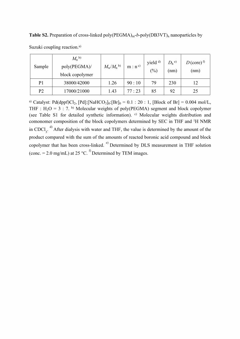
Table S2. Preparation of cross-linked poly(PEGMA)m-b-poly(DB3VT)n nanoparticles by
Suzuki coupling reaction.a)
a) Catalyst: Pd(dppf)Cl2, [Pd]:[NaHCO3]0:[Br]0 = 0.1 : 20 : 1, [Block of Br] = 0.004 mol/L,
THF : H2O = 3 : 7. b) Molecular weights of poly(PEGMA) segment and block copolymer (see Table S1 for detailed synthetic information). c) Molecular weights distribution and comonomer composition of the block copolymers determined by SEC in THF and 1H NMR
in CDCl3. d) After dialysis with water and THF, the value is determined by the amount of the
product compared with the sum of the amounts of reacted boronic acid compound and block
copolymer that has been cross-linked. e) Determined by DLS measurement in THF solution
(conc. = 2.0 mg/mL) at 25 °C. f) Determined by TEM images.
Sample
Mn b)
poly(PEGMA)/
block copolymer
Mw/Mn b) m : n c)
yield d)
(%)
Dh e)
(nm)
D (core) f)
(nm)
P1 38000/42000 1.26 90 : 10 79 230 12
P2 17000/21000 1.43 77 : 23 85 92 25

Table S3. Electrical performance of the studied transistor-type memory devices using cross-linked
poly(PEGMA)m-b-poly(DB3VT)n nanoparticles as dielectric layer. a)
a) The data were averaged from at least 10 devices of two different batches. b) Determined by TEM
images. c) On/off drain current ratios of reading at Vg = −5 V. d) VThP is the threshold voltage after
programming progress and VThH
is that after erasing progress. e) Memory window is defined as VThP
− VThE for reversible device and as VTh
P − VThInitial for WORM-type device.
Dielectric layer m : n D (core)
(nm) b)
Mobility × 10-3
(cm2 V-1 s-1)ION/IOFF c)
VthP
(V) d)
VthE
(V) d)
Memory
window (V) e)
Poly(PEGMA) - - 3.9 ± 0.14 3.3 × 10⁵ 3 3 -
P1 90 : 10 12 1.4 ± 0.62 3.4 × 10⁵ −25 0 25 (FLASH)
P2 77 : 23 25 2.5 ± 0.21 5.1 × 10⁵ −34 0 34 (FLASH)
Poly(DB3VT) - - 6.6 ± 0.20 9.7 × 10⁶ −10 −10 10 (WORM)

Scheme S1. Synthesis of poly(PEGMA)-b-poly(DB3VT).

Scheme S2. Preparation of cross-linked core-shell nanoparticles by the Suzuki coupling
reaction.

1,4-Dioxane60 oC 24 h
S
S
S
S
SBr
Br
nAIBN,
CTA
SBr
Br
Scheme S3. Preparation of poly(DB3VT) homopolymer by the RAFT polymerization.
0246810 ppm
CDCl3
j
cd,e,f,g
H2O
b,h a
i
Figure S1. 1H NMR spectra of (a) poly(DB3VT) (top), the peaks corresponding to terminal
CTA are marked, and (b) poly(PEGMA)77-b-Poly(DB3VT)23 (bottom) in CDCl3.
O OS
Br
Br
n
O
O3-4
a b
cd
ef
g
h i
jm
(a)
(b)
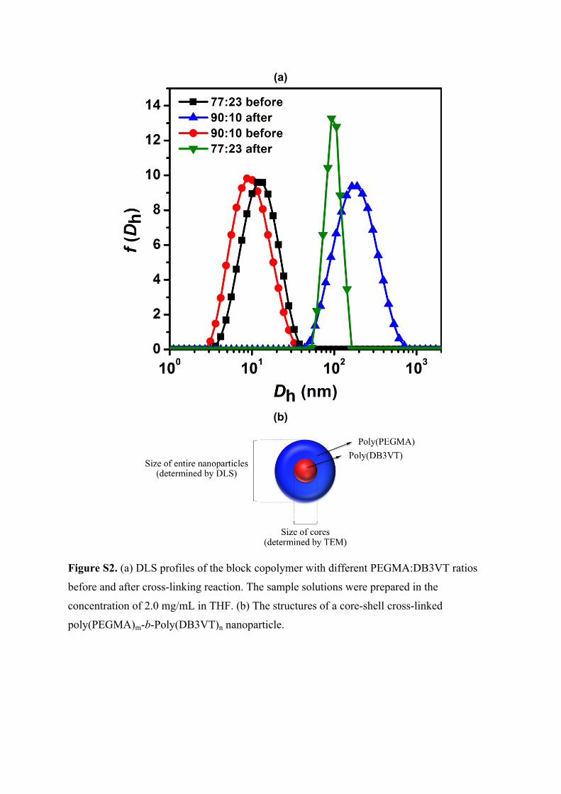
Figure S2. (a) DLS profiles of the block copolymer with different PEGMA:DB3VT ratios
before and after cross-linking reaction. The sample solutions were prepared in the
concentration of 2.0 mg/mL in THF. (b) The structures of a core-shell cross-linked
poly(PEGMA)m-b-Poly(DB3VT)n nanoparticle.
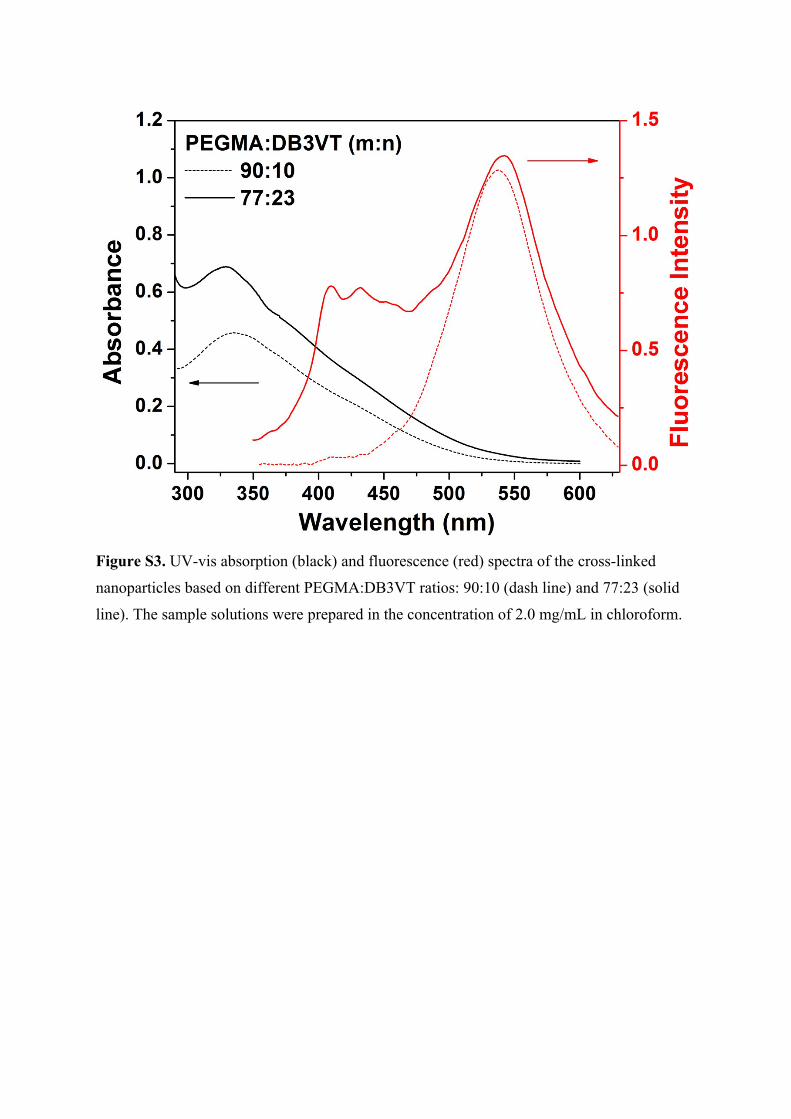
Figure S3. UV-vis absorption (black) and fluorescence (red) spectra of the cross-linked
nanoparticles based on different PEGMA:DB3VT ratios: 90:10 (dash line) and 77:23 (solid
line). The sample solutions were prepared in the concentration of 2.0 mg/mL in chloroform.

Figure S4. AFM height (a-b) and TEM (i-ii) images of the spin-coat thin film of studied
nanoparticles (from 3.0 mg/mL in chloroform) with different PEGMA:DB3VT ratios: (a)(i)
90:10 and (b)(ii) 77:23.

Fig S5. The particle size distribution histograms based on the TEM images of the spin-coat
thin films from the cross-linked poly(PEGMA)m-b-poly(DB3VT)n nanoparticles: P1 (upper)
and P2 (lower).

Figure S6. AFM height (a-b) and TEM (i-ii) images of the spin-coat thin film of studied
nanoparticles (from 1.0 mg/mL in chloroform) with different PEGMA:DB3VT ratios: (a)(i)
90:10 and (b)(ii) 77:23.

Figure S7. TEM images of the spin-coat thin film of studied poly(DB3VT) homopolymer in
two different scales (3.0 mg/mL in chloroform).

Figure S8. AFM height images of the pentacene layer deposited onto the spin-coat thin films
of studied nanoparticles (from 3.0 mg/mL in chloroform) with different PEGMA:DB3VT
ratios: (a) 90:10 and (b) 77:23.

Figure S9. Energy diagram and the proposed charge-trapping mechanism: pentacene and
both moieties of the studied cross-linked poly(PEGMA)m-b- poly(DB3VT)n nanoparticles.

Figure S10. Transfer characteristics of the OFET memory devices using poly(DB3VT)
homopolymer as dielectric layer: the device was first programmed using –50 V gate bias (P)
for 1 s, and then was respectively erased using 50 V gate bias (E) for 1 s, 3 s, 5 s, and 7 s.
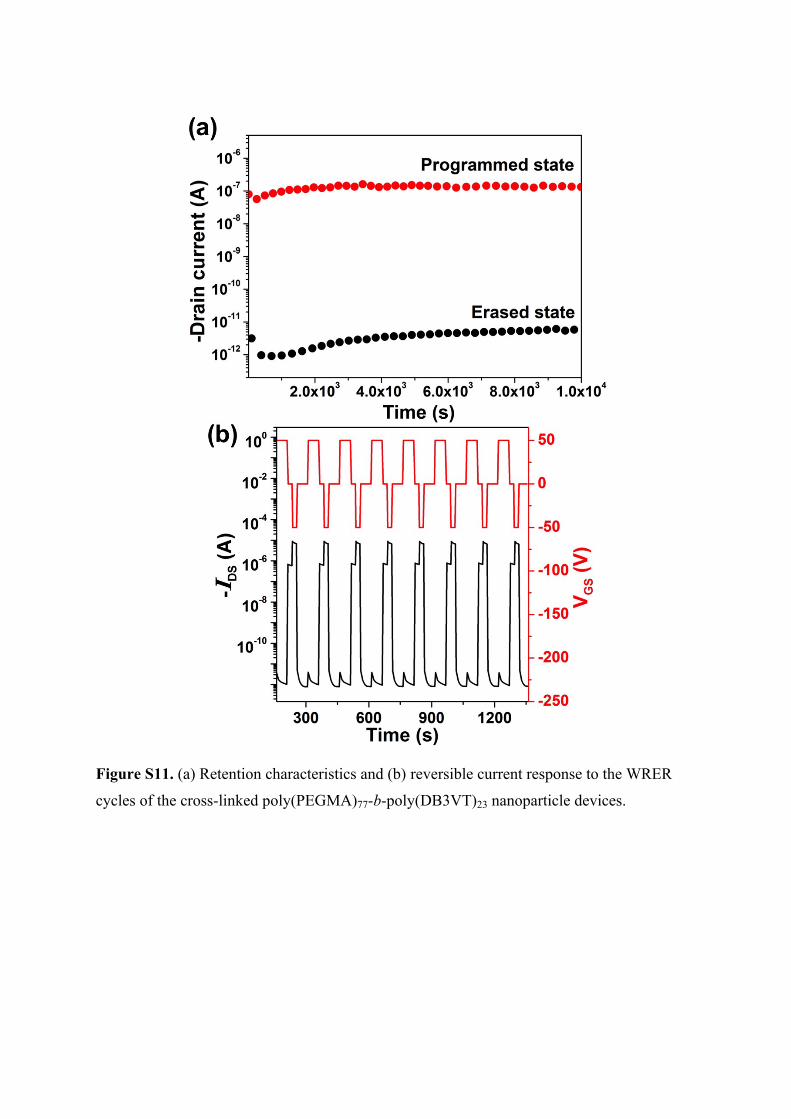
Figure S11. (a) Retention characteristics and (b) reversible current response to the WRER
cycles of the cross-linked poly(PEGMA)77-b-poly(DB3VT)23 nanoparticle devices.

Figure S12. Retention characteristics of the device using poly(DB3VT) homopoylmer as
dielectric layer.