supporting information - royal society of chemistry · supporting information hybrid chemical vapor...
TRANSCRIPT

1
Supporting Information Hybrid chemical vapor deposition enables scalable and stable Cs-FA mixed cation perovskite solar modules with a designated area of 91.8 cm2 approaching 10% efficiency Longbin Qiu,†a Sisi He,†a Yan Jiang,a Dae-Yong Son,a Luis K. Ono,a Zonghao Liu,a Taehoon Kim,a Theodoros Bouloumis,a Said Kazaoui,b Yabing Qi*a † L. Qiu and S. He contributed equally to this work. a. Energy Materials and Surface Sciences Unit (EMSSU), Okinawa Institute of Science and Technology Graduate University (OIST), 1919-1 Tancha, Kunigami-gun, Onna-son, Okinawa 904-0495, Japan. *Corresponding author: Yabing Qi, E-mail: [email protected] b. Research Center for Photovoltaics (RCPV), National Institute of Advanced Industrial Science and Technology (AIST), Tsukuba, Ibaraki 305-8565, Japan
Electronic Supplementary Material (ESI) for Journal of Materials Chemistry A.This journal is © The Royal Society of Chemistry 2019

2
Figure S1. Tauc-plot of the Cs0.1FA0.9PbI2.9Br0.1 perovskite film exhibiting an optical band-gap of 1.56 eV.
3
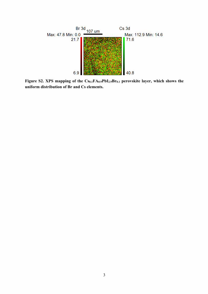
Figure S2. XPS mapping of the Cs0.1FA0.9PbI2.9Br0.1 perovskite layer, which shows the uniform distribution of Br and Cs elements.

4
Figure S3. XRD data of the Cs0.1FA0.9PbI2.9Br0.1 perovskite film by the CVD process and the solution coating process.

5
Figure S4. a) Absorbance and the corresponding b) Tauc-plots of the Cs0.1FA0.9PbI2.9Br0.1 perovskite films by the CVD process and the solution coating process.

6
Figure S5. XPS spectra of the Br 3d core level of the Cs0.1FA0.9PbI2.9Br0.1 perovskite film by the CVD process and the solution coating process.
7
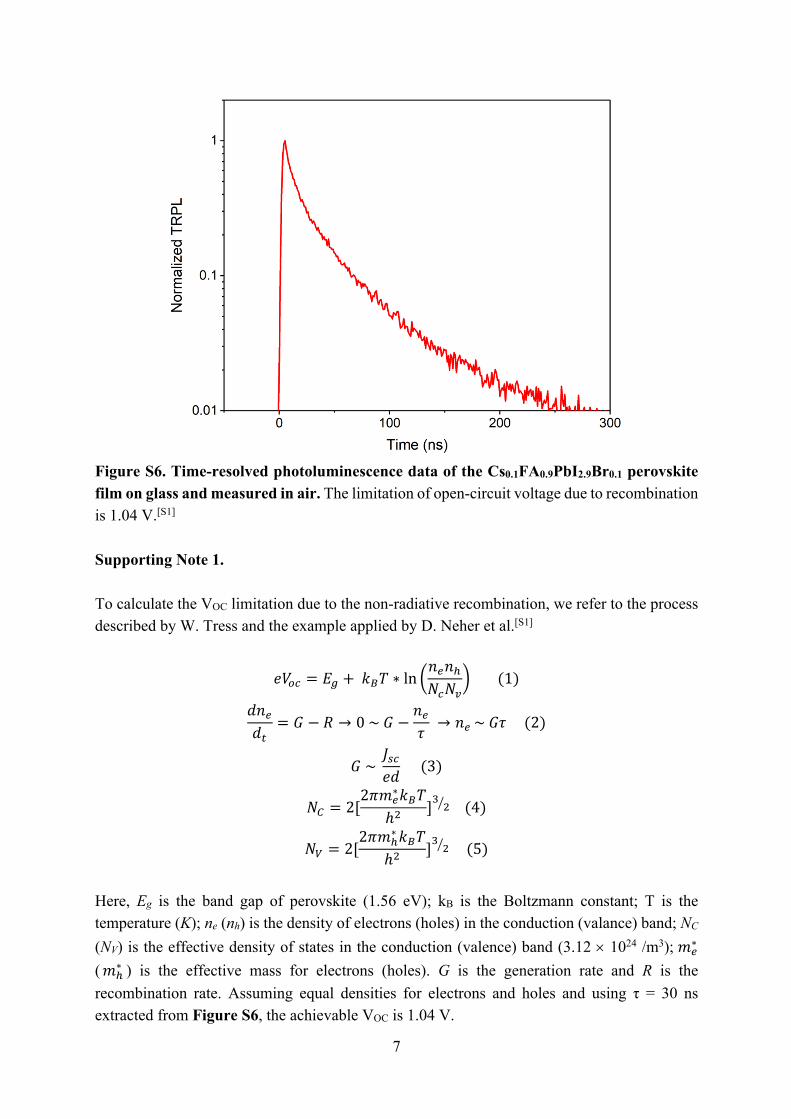
Figure S6. Time-resolved photoluminescence data of the Cs0.1FA0.9PbI2.9Br0.1 perovskite film on glass and measured in air. The limitation of open-circuit voltage due to recombination is 1.04 V.[S1] Supporting Note 1. To calculate the VOC limitation due to the non-radiative recombination, we refer to the process described by W. Tress and the example applied by D. Neher et al.[S1]
𝑒𝑉#$ = 𝐸' +𝑘+𝑇 ∗ ln 0𝑛2𝑛3𝑁$𝑁5
6(1)
𝑑𝑛2𝑑;
= 𝐺 − 𝑅 → 0~𝐺 −𝑛2𝜏 → 𝑛2~𝐺𝜏(2)
𝐺~𝐽E$𝑒𝑑 (3)
𝑁G = 2[2𝜋𝑚2
∗𝑘+𝑇ℎL ]N LO (4)
𝑁Q = 2[2𝜋𝑚3
∗𝑘+𝑇ℎL ]N LO (5)
Here, Eg is the band gap of perovskite (1.56 eV); kB is the Boltzmann constant; T is the temperature (K); ne (nh) is the density of electrons (holes) in the conduction (valance) band; NC (NV) is the effective density of states in the conduction (valence) band (3.12 ´ 1024 /m3); 𝑚2
∗ (𝑚3
∗ ) is the effective mass for electrons (holes). G is the generation rate and R is the recombination rate. Assuming equal densities for electrons and holes and using τ = 30 ns extracted from Figure S6, the achievable VOC is 1.04 V.

8
Figure S7. Typical J-V curves with sputtered SnO2 as electron transport layer for the HCVD grown perovskite Cs0.1FA0.9PbI2.9Br0.1 based devices.

9
Figure S8. Secondary electron cutoff (work function determination) and valance band spectra (shown in log scale) of the SnO2 film before and after the vacuum annealing process.

10
Figure S9. XPS a) Sn 3d and b) O 1s core level spectra of the SnO2 film before and after vacuum annealing. After vacuum annealing the O content decreased by 4% (with the Sn content normalized to 1).

11
Figure S10. Typical J-V curves with SnO2 and vacuum annealed SnO2 as electron transport layer for spin coated perovskite based devices.
12
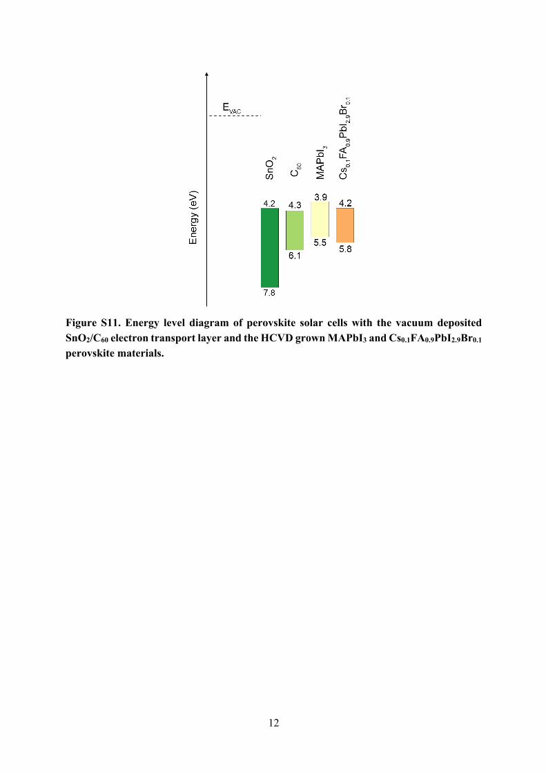
Figure S11. Energy level diagram of perovskite solar cells with the vacuum deposited SnO2/C60 electron transport layer and the HCVD grown MAPbI3 and Cs0.1FA0.9PbI2.9Br0.1 perovskite materials.

13
Figure S12. Solar module patterning for sub-cell interconnection with a geometric fill factor of 0.9.

14
Figure S13. Side view of the perovskite solar modules after encapsulation.

15
Figure S14. 10 cm ́ 10 cm Cs0.1FA0.9PbI2.9Br0.1 solar module performance before and after encapsulation.

16
Figure S15. Solar cell efficiency decays as a function of cell/module designated area for both champion and average solar cell/module performance (decay rate 1.3% per decade).

17
Figure S16. Hysteresis of the HCVD fabricated Cs0.1FA0.9PbI2.9Br0.1 solar module with an area of 10 cm ´ 10 cm.

18
Figure S17. 10 cm ´ 10 cm HCVD fabricated MAPbI3 solar module performance. a. J-V curves before and after encapsulation shows a similar PCE of approximately 6.4%. b. Steady-state power output at the bias voltage of 8.4 V shows the stabilized PCE of 5.9%.
19
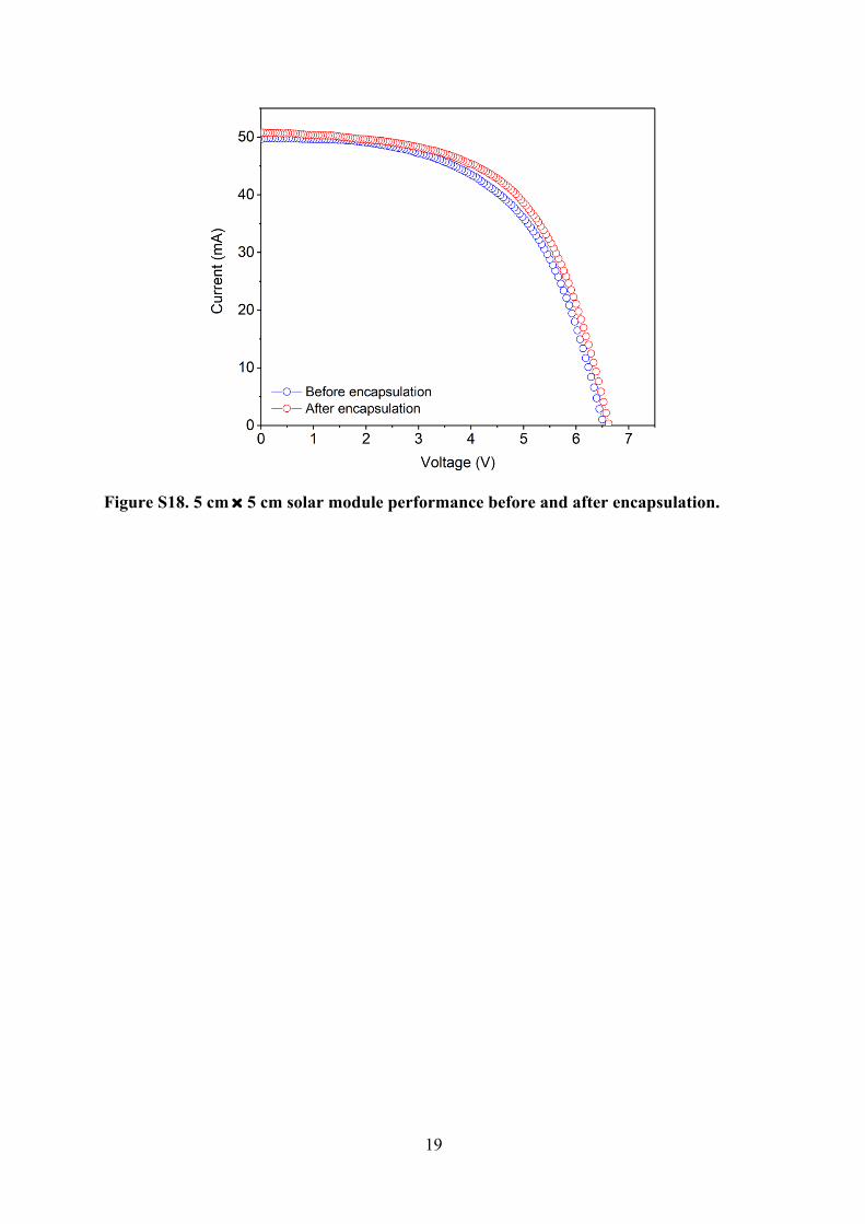
Figure S18. 5 cm ´ 5 cm solar module performance before and after encapsulation.

20
Table S1. Binding energy for the XPS core levels of Cs 3d and Pb 4f before and after HCVD.
Cs 3d3/2 (eV) Cs 3d5/2 (eV) Pb 4f5/2 (eV) Pb 4f7/2 (eV) PbI2/CsBr 738.1 724.2 142.8 137.9
Cs0.1FA0.9PbI2.9Br0.1 738.8 724.8 143.2 138.3

21
Table S2. Photovoltaic parameters for the HCVD fabricated devices based on SnO2 and SnO2/C60 electron transport layer.
ETL VOC (V) JSC (mA/cm2) FF PCE (%) SnO2 0.81 ± 0.07 18.4 ± 0.5 0.54 ± 0.04 8.1 ± 1.1
SnO2/C60 0.90 ± 0.04 20.2 ± 0.3 0.67 ± 0.02 12.3 ± 0.6

22
Table S3. Photovoltaic parameters for the solution coated perovskite devices based on different SnO2 with and without the vacuum annealing treatment.
SnO2 treatment VOC (V) JSC (mA/cm2) FF PCE (%)
Sputtered SnO2
Without vacuum annealing
1.03 ± 0.01 21.4 ± 0.2 0.74 ± 0.02 16.4 ± 0.5
With vacuum annealing
0.73 ± 0.04 18.8 ± 0.9 0.55 ± 0.02 7.6 ± 0.6
Alfa Aesar SnO2
(solution coating)
Without vacuum annealing
1.06 ± 0.01 20.2 ± 0.3 0.72 ± 0.04 15.5 ± 0.8
With vacuum annealing
0.96 ± 0.02 19.6 ± 0.2 0.62 ± 0.04 11.7 ± 0.9
SnO2/C60
Without vacuum annealing
1.02 ± 0.01 20.7 ± 0.6 0.68 ± 0.02 14.4 ± 0.7
With vacuum annealing
1.00 ± 0.02 20.6 ± 0.5 0.66 ± 0.03 13.6 ± 0.7

23
Table S4. Photovoltaic parameters for the 10 cm ´ 10 cm perovskite solar modules with a designated area of 91.8 cm2 fabricated using the HCVD method.
Number VOC (V) JSC (mA/cm2) FF PCE (%) 1 12.92 1.17 0.53 8.06 2 12.60 1.10 0.56 7.74 3 13.04 1.22 0.58 9.17 4 12.54 1.22 0.55 8.40 5 12.34 1.21 0.52 7.83 6 12.44 1.19 0.56 8.37 7 12.49 1.19 0.55 8.20 8 13.55 1.16 0.59 9.34 9 13.45 1.14 0.58 8.82 10 12.60 1.13 0.52 7.36
Average 12.8 ± 0.4 1.17 ± 0.04 0.55 ± 0.02 8.3 ± 0.6

24
[S1] (a) W. Tress, Adv. Energy Mater. 2017, 7, 1602358; (b) M. Stolterfoht, C. M. Wolff, J. A. Márquez, S. Zhang, C. J. Hages, D. Rothhardt, S. Albrecht, P. L. Burn, P. Meredith, T. Unold, D. Neher, Nat. Energy 2018, 3, 847.