superconducting receiver front-end and its application in … · 2018-09-25 · microwave passive...
TRANSCRIPT

19
Superconducting Receiver Front-End and Its Application In Meteorological Radar
Yusheng He and Chunguang Li Institute of Physics, Chinese Academy of Sciences, Beijing 1000190,
China
1. Introduction
The discovery of superconductivity is one of the greatest achievements in fundamental sciences of 20th century. Nearly one hundred year ago, the Dutch physicist H. Kamerlingh Onnes found that the resistance of pure mercury abruptly dropped to zero at liquid helium temperature 4.2K (Kammerlingh Onnes, 1911). Since then scientists tried very hard to find more superconducting materials and to understand this microscopic quantum phenomenon, which has greatly pushed forward the development of modern physics. Enormous progress has been made since 1986, when the so called high temperature superconductors (HTS) were discovered (Bednorz & Mueller, 1986). Superconductivity becomes not only a branch of fundamental sciences but also a practical technology, ready for applications. It is commonly recognized that the first application of HTS thin films is in high performance microwave passive devices, especially filters. As a successful example the application of HTS filter in meteorological radar will be introduced. In this chapter firstly the fundamental concepts of superconductivity will be summarized and then the basic principles of superconducting technology at microwave frequency will be briefly outlined. Then the design and construction of superconducting filters and microwave receiver front-end subsystems will be discussed. Finally results of field trial of the world first superconducting meteorological radar will be introduced and conclusions will then be drawn.
2. Superconductivity and superconducting technology at microwave frequency
2.1 Basic concepts of superconductivity Superconductivity is a microscopic quantum mechanical phenomenon occurring in certain materials generally at very low temperatures, characterized by exactly zero DC electrical resistance and the exclusion of the interior magnetic field, the so called Meissner effect (Meissner & Ochsenfeld, 1933). Superconductivity is a thermodynamic phase of condensed matters, and thus possesses certain distinguishing properties which are largely independent of microscopic details. For example, the DC resistance of a superconductor drops abruptly to zero when the material is cooled below its "critical temperature Tc ". Conventional superconductors are in a wide variety, including simple elements like Al, Pb and Nb, various metallic alloys (e.g., Nb-Ti alloy) and compounds (e.g., Nb3Sn) as well as some strong correlated systems (Heavy Fermions). As of 2001, the highest critical temperature
Source: Radar Technology, Book edited by: Dr. Guy Kouemou, ISBN 978-953-307-029-2, pp. 410, December 2009, INTECH, Croatia, downloaded from SCIYO.COM
www.intechopen.com
Radar Technology
386
found for a conventional superconductor is 39 K for MgB2, although this material displays enough exotic properties that there is doubt about classifying it as a "conventional" superconductor. A revolution in the field of superconductivity occurred in 1986 (Bednorz & Mueller, 1986) and one year later a family of cuprate-perovskite ceramic materials was discovered with superconducting transition temperature greater than the boiling temperature of liquid nitrogen, 77.8 K, which are known as high temperature superconductors (hereinafter referred to as HTS). Examples of HTS include YBa2Cu3O7, one of the first discovered and most popular cuprate superconductors, with transition temperature Tc at about 90 K and Tl2Ba2CaCu2O8, HgBa2Ca2Cu3O8, of which the mercury-based cuprates have been found with Tc in excess of 130 K. These materials are extremely attractive because not only they represent a new phenomenon not explained by the current theory but also their superconducting states persist up to more manageable temperatures, beyond the economically-important boiling point of liquid nitrogen, more commercial applications are feasible, especially if materials with even higher critical temperatures could be discovered. Superconductivity has been well understood by modern theories of physics. In a normal conductor, an electrical current may be visualized as a fluid of electrons moving across a heavy ionic lattice. The electrons are constantly colliding with the ions in the lattice, and during each collision some of the energy carried by the current is absorbed by the lattice and converted into heat, which is essentially the vibrational kinetic energy of the lattice ions. As a result, the energy carried by the current is constantly being dissipated. This is the phenomenon of electrical resistance. The situation is different in a superconductor, where part of the electrons is bounded into pairs, known as Cooper pairs. For conventional superconductors this pairing is caused by an attractive force between electrons from the exchange of phonons whereas for HTS, the pairing mechanism still being an open question. Due to quantum mechanics, the energy spectrum of this Cooper pair fluid possesses an energy gap, meaning there is a minimum amount of energy ΔE that must be supplied in order to break the pair into single electrons. In the superconducting state, all the cooper pairs act as a group with a single momentum and do not collide with the lattice. This is known as the macroscopic quantum state and explains the zero resistance of superconductivity. More over, when a superconductor is placed in a weak external magnetic field H, the field penetrates the superconductor only a small distance λ, called the London penetration depth, decaying exponentially to zero within the bulk of the material. This is called the Meissner effect, and is a defining characteristic of superconductivity. For most superconductors, the London penetration depth λ, is on the order of 100 nm.
2.2 Superconductivity at microwave frequency As mentioned above, in a superconductor at finite temperatures there will be normal electrons as well as Cooper pairs, which has been successfully depicted by an empirical two-fluid model, proposed by Gorter and Casimir (Gorter & Casimir, 1934). In this model it simply assumes that the charge carriers can be considered as a mixture of normal and superconducting electrons, which can be expressed as n=nn+ns, where n, nn, ns are the numbers of total, normal and superconducting electrons, respectively, and ns=fn, nn=(1-f)n. The superconducting fraction f increases from zero at Tc to unity at zero temperature. At microwave frequencies, the effect of an alterative electromagnetic field is to accelerate both parts of carriers or fluids. The normal component of the current will dissipate the gained
www.intechopen.com

Superconducting Receiver Front-End and Its Application In Meteorological Radar
387
energy by making collisions with lattice. In the local limit the conductance of a superconductor can be represented by a complex quantity
1 2jσ σ σ= − (1)
where the real part σ1 is associated with the lossy response of the normal electrons and the imaginary part is associated with responses of both normal and superconducting electrons. In his book (Lancaster, 1997) M. J. Lancaster proposed a simple equivalent circuit, as shown in Fig. 1, to describe the physical picture of the complex conductivity. The total current J in the superconductor is split between the reactive inductance and the dissipative resistance. As the frequency decreases, the reactance becomes lower and more and more of the current flows through the inductance. When the current is constant this inductance completely shorts the resistance, allowing resistance –free current flow.
Fig. 1. Equivalent circuit depicting complex conductivity (Lancaster, 1997)
The microwave properties are determined by currents confined to the skin-depth, in the
normal metal state and to the penetration depth, λ, in the superconducting state. The surface impedance of a superconductor should be considered, which is defined as
0Z
ExZs Rs jXs
Hy =
⎛ ⎞= = +⎜ ⎟⎝ ⎠ (2)
where Ex and Hy are the tangential components of the electric and magnetic fields at the surface (z=0). For a unit surface current density, the surface resistance Rs is a measure of the rate of energy dissipation in the surface and the surface reactance Xs is a measure of the peak inductive energy stored in the surface. Relating to the complex conductivity, the surface impedance can be then written as
1
20
1 2
jZs
j
ωμσ σ⎛ ⎞= ⎜ ⎟−⎝ ⎠ (3)
In the case of the temperature is not too close to Tc, where more superconducting carriers are
present, and σ1 is finite but much smaller than σ2, approximation of σ1<< σ2 can be made. It then turns out that
2 2 30 1 0
1
2Zs jω μ λ σ ωμ λ= + (4)
with the frequency independent magnetic penetration depth ( )1/220/ sm n eλ μ= , where m is
the mass of an electron and e is the charge on an electron.
www.intechopen.com

Radar Technology
388
From Equation (2), important relations for surface resistance and reactance can be easily derived,
2 2 30 1
1
2Rs ω μ λ σ= (5)
and
0Xs ωμ λ= (6)
It is well known that for a normal metal, the surface resistance increases with ω1/2, whereas
for a superconductor, that increases with ω2 (Equation 5). Knowledge of the frequency dependence of the surface resistance is especially important to evaluate potential microwave applications of the superconductor. It can be seen from Fig. 2 that YBa2Cu3O7 displays a lower surface resistance compared to Cu up to about 100 GHz.
Fig. 2. Frequency dependence of surface resistance of YBa2Cu3O7 compared with Cu .
2.3 Superconducting thin films for microwave device applications Superconducting thin films are the main constituent of many of the device applications. It is important for these applications that a good understanding of these films is obtained. Superconducting thin films have to be grown on some kind of substrates which must meet certain requirements of growth compatibility, dielectric property and mechanical peculiarity in order to obtain high quality superconducting films with appropriate properties for microwave applications. First of all the substrates should be compatible with film growth. In order to achieve good epitaxial growth the dimensions of the crystalline lattice at the surface of the substrate should match the dimensions of the lattice of the superconductor, otherwise strains can be set up in the films, resulting in dislocations and defects. Chemical compatibility between superconductors and the substrates are also important since impurity levels may raise if the substrate reacts chemically with the superconductor or atomic migrations take place out of the substrate. Appropriate match between the substrate and the film in thermal expansion is also vital so as to avoid cracks during repeated cooling and warming processes. For dielectric properties, the most important requirement is low enough dielectric tangent loss, without which the advantage of using superconducting film will be
www.intechopen.com
Superconducting Receiver Front-End and Its Application In Meteorological Radar
389
counteracted. The high value of dielectric constant is also good for the miniature of the microwave devices. It should be convenient and easier for the design if the dielectric constant is isotropic in the plane of the film. From the machining and processing point of view, the surface of the substrate should be smooth and free from defects and twinning if possible. It should also be mechanically strong, environmentally stable, and capable of being thinned to a certain extent. As a matter of fact, no existing substrate can meet all of the above requirements. Some of the problems can be overcome by certain technologies, e.g., introduction of buffer layer between the films and the substrates. There are indeed a number of good substrates being used and excellent superconducting films with satisfactory microwave properties were produced on them. Table 1 shows the common used substrates for HTS thin films in microwave device applications.
Substrate εr (typical) tgδ (typical)
LaAlO3 24.2@77K 7.6×10⁻⁶@77K and 10GHz
MgO 9.6@77K 5.5×10⁻⁶@77K and 10GHz
11.6∥c-axis @77K Sapphire
9.4⊥c-axis @77K 1.5×10⁻⁸@77K and 10GHz
Table 1. Substrates of HTS thin films for microwave device applications
The properties of superconducting thin films and their suitability for microwave devices are critically dependent on processing. So far almost all HTS thin film microwave devices have been fabricated from two materials, i.e., YBa2Cu3O7 (Tc~85-93 K in thin film form) of which element Y may be substitute by some other rare-earth elements, e. g., Dy and Tl2Ba2CaCu2O8 (Tc ~100-110 K in thin film form). There is a variety of methods for preparing superconducting thin films, including pulsed laser ablation, magnetron sputtering, and evaporation etc. In principle, a film in some kind precursor phase is grown first and then followed by in-situ or post-deposition anneal treatments. For example, oxygen deficient
YBa2Cu3O6 phase can be grown at about 850°C, which is later converted into the YBa2Cu3O7
phase by a low temperature (~500°C) anneal in oxygen atmosphere. Using this process
YBa2Cu3O7 (or more accurately YBa2Cu3O7-δ, with δ<1) films can be made with surface resistance at the order of a few hundred micron ohms. Handling of HTS films must be with great care. Once formed the properties of the films can
degrade under some environmental conditions. Aqueous environments are very deleterious.
Therefore the superconducting films should be always kept dry and away from water
vapour. Care must be also exercised during all fabrication processes. A protection layer on
the top of the superconducting patterns of the devices will be helpful. It should be advised,
however, to keep the devices always away from humidity.
2.4 Superconducting transmission lines In microwave circuits, a transmission line is the material medium or structure that forms all
or part of a path from one place to another for directing the transmission of electromagnetic
waves. It not only serves as interconnections between components in the circuits, but also
often forms the basic element of components and devices. It is indeed the foundation of the
microwave circuits and most microwave theories are originated directly or indirectly from
transmission theory, which is also true for superconducting devices.
www.intechopen.com
Radar Technology
390
The most important effect of superconducting transmission lines is their very low loss. A superconducting transmission line is dispersionless, provided the wave propagated is in a TEM mode. This is due to that the penetration depth is not varying with frequency, contrasting with normal conductors where the skin depth is a function of frequency. The realistic transmission line model represents the transmission line as an infinite series of two-port elementary components, each representing an infinitesimally short segment of the transmission line with distributed resistance R, inductance L, and capacitance C. Commonly used transmission lines include wires, coaxial cables, dielectric slabs, optical fibers, electric power lines, waveguides, and planar transmission lines etc. Considering most superconducting filters are based on superconducting films, in this book we will concentrate on the planar transmission lines, i.e., microstrip, coplanar, and stripline. Microstrip is a widely used type of microwave transmission line which consists of a conducting strip with a width w and a thickness t separated from a ground plane by a
dielectric layer known as the substrate with a dielectric constant ε and a thickness d. The general structure of a microstrip is shown schematically in Fig. 3 (a). The fields in the microstrip extend within two media: air above and dielectric below and in general, the dielectric constant of the substrate will be greater than that of the air, so that the wave is traveling in an inhomogeneous medium. In consequence, the propagation velocity is somewhere between the speed of microwaves in the substrate and the speed of microwaves in air. This behavior is commonly described by stating the effective dielectric constant (or effective relative permittivity) of the microstrip; this being the dielectric constant of an equivalent homogeneous medium. Due to this inhomogeneous nature, the microstrip line will not support a pure TEM wave; both the E and H fields will have longitudinal components. The longitudinal components are small however, and so the dominant mode is referred to as quasi-TEM. The field propagation velocities will depend not only on the material properties but also on the physical dimensions of the microstrip. Comparing to other transmission lines, e.g., the traditional waveguide technology, the advantage of microstrip is much less expensive as well as being far lighter and more compact. Whereas the disadvantages of microstrip compared with waveguide are the generally lower power handling capacity, and higher losses, of which, the later can be greatly improved by employing superconducting materials.
(a) (b) (c)
Fig. 3. Cross-section geometries of microstrip (a), coplanar line (b), and stripline (c).
A coplanar line is formed from a conductor separated from a pair of ground planes, all on the same plane, at the top of a dielectric medium. In the ideal case, the thickness of the dielectric is infinite; in practice, it should be thick enough so that EM fields die out before they get out of the substrate. The advantages of coplanar line are that active devices can be mounted on top of the circuit, like on microstrip. More importantly, it can provide extremely high frequency response (100 GHz or more) since connecting to coplanar line does not entail any parasitic discontinuities in the ground plane. For superconducting
www.intechopen.com
Superconducting Receiver Front-End and Its Application In Meteorological Radar
391
coplanar line it means only single side superconducting film is required, which will greatly reduce the difficulties in film making since double-sided films need special technology, especially for those newly discovered superconductors. One of the disadvantages of the coplanar line is the imbalance in the ground planes, although they are connected together at some points in the circuit. The potential of the ground planes can become different on each side, which may produce unwanted mode and interference. The problem can be solved in some extent by connecting the two ground planes some where in the circuit with “flying wire” (air bridge) over the conducting plane. It, however, will bring complexity and other problems. A standard stripline uses a flat strip of metal which is sandwiched between two parallel ground planes. The width of the strip, the thickness of the substrate (the insulating material between the two ground plans) and the relative permittivity of the substrate determine the characteristic impedance of the transmission line. The advantage of the stripline is that the radiation losses are eliminated and a pure TEM mode can be propagated in it. The disadvantage of stripline is the difficulty in construction, especially by superconducting films. It requires two pieces of superconducting films of both double-sided or one single- plus one double-sided film. The air gap, though extremely small, will cause perturbations in impedance and to form contacts to external circuits is also very difficult. Besides, if two pieces of double-sided films employed, the precise aiming between the very fine patterns of two films brings another problem.
2.5 Application of transmission lines: Superconducting resonators A microwave resonator is a simple structure which can be made of cavity or transmission line and is able to contain at least one oscillating electromagnetic field. If an oscillating field is set up within a resonator it will gradually decay because of losses. By using superconductors the losses can be greatly reduced and high Q-values can be than achieved. Resonators are the most fundamental building blocks in the majority of microwave circuits. By coupling a number of resonators together, a microwave filter can be constructed. A high Q-resonator forms the main feed back element in a microwave oscillator. The quality factor for a resonator is defined by
0 2w
Qp
π= (7)
where w is the energy stored in the resonator, and p is the dissipated energy per period in the resonator. The losses in a resonator arise due to a number of mechanisms. The most important are usually the losses associated with the conduction currents in the conducting layer of the cavity or transmission line, the finite loss tangent of dielectric substrate and radiation loss from the open aperture. The total quality factor can be found by adding these losses together, resulting in
0
1 1 1 1
c d rQ Q Q Q= + + (8)
where Qc, Qd, and Qr are the conductor, dielectric and radiation quality factors, respectively. For conventional cavity or transmission line resonators at microwave frequency, usually Qc
dominates. This is why superconductor can greatly increase the Q-value of the resonators.
www.intechopen.com

Radar Technology
392
For superconducting resonators, the resonant frequency and Q value are temperature dependent and the variation is remarkable when close to Tc, as shown in Fig.4 (Li, H. et al., 2002). It is therefore preferable to operator at a temperature below 80% of Tc, where more stable resonant frequency and high enough Q value being achieved.
Fig. 4. Temperature dependence of resonate frequency and Q value of superconducting resonator (Li, H. et al., 2002)
Beside the Q-value, size is also important to HTS resonator not only because the commercial consideration for reducing the cost but also because that the HTS filters need to work at low temperature and large size will increase burden of the cryo-cooler. However, the high quality factor and the minimized size are often a pair of contradiction, because the reduction of the size always causes the reduction of the stored energy and hence the Q-vales. The quality factors and volumes of various kinds of HTS resonators are shown in Fig.5 in dual-log coordinate at frequency around 5 GHz. All the data come from literatures published over the last decades. Here the volume of the planar resonators is calculated by assuming it has a height of 8 mm.
10 100 1000 10000 100000
1000
10000
100000
Qu
Volume( mm3)
Cavity
Dielectric
CPW
Microstrip
Patch
Fig. 5. The quality factor vs. volume of different kind of HTS resonators
HTS Cavity resonators are usually designed to resonate in the TE011 mode. In this mode, the current flow is circumferential, so there is no current flow across the joint of the side wall and the end plates. Although such structures have very high Q-values, their volume becomes prohibitively large at low frequencies. HTS dielectric resonators usually consist of a
www.intechopen.com

Superconducting Receiver Front-End and Its Application In Meteorological Radar
393
dielectric rod of single crystal material sandwiched between two planar HTS films. They can have very high Q-values (if very large area high quality superconducting films applied), but are smaller than unloaded resonant cavities. Due to their large volume and difficulty in realizing cross couplings, HTS Cavity resonators and HTS dielectric resonators are often used to construct low phase-noise oscillators and, for the dielectric ones, to measure the surface resistance of HTS thin films. They are seldom used in filters. Patch resonators, which are two dimensional resonators, are of interest for the design of high power handling HTS filters. An associated advantage of them is their lower conductor losses as compared with one dimensional line resonators. However, patch resonators tend to have stronger radiation, so they are not suitable for designing narrow band filters. The frequently used one dimensional HTS transmission line resonators in applications are Coplanar Waveguide (CPW) resonators and Microstrip resonators. Because the circuit structure and the ground planes are fabricated on a single plane, CPW resonators offer the possibility of integration with active components. But the electromagnetic energy in the CPW resonators are more confined to a small area between the HTS line and the grounds so they tend to have lower quality factors compared to other type of HTS resonators. Microstrip resonators are the most popular type of resonators used in HTS microwave filters. Besides their relatively high quality factor and small size, the ease with which they can be used in a variety of coupling structures is a big advantage. For most applications the basic shape of a HTS microstrip resonator is a half-wavelength (Fig. 6 (a)) line instead of the grounded quarter-wavelength
(λ/4) line, due to the difficulty in realizing ground via HTS substrate. The conventional λ/2 resonators can be miniaturized by folding its straight rectangular ribbon. The height of a
folded resonator, called a hairpin resonator (Fig. 6 (b)), is usually less than λ/4. Meander-line resonators (Fig. 6 (c)), meander-loop resonators (Fig. 6 (d)), spiral resonators (Fig. 6 (e)) and spiral-in-spiral-out resonators (Fig. 6 (f)) can be considered as modifications of
conventional straight ribbon (λ/2) resonators by folding the ribbons several times and in
different ways. In principle, the λ/2 resonators can be folded or transformed to any other shapes according to the demands of miniaturization or other purpose.
Fig. 6. Typical one dimensional microstrip resonators: (a) half-wave length line resonator; (b) hairpin resonator; and (c) to (f) other open loop resonators.
2.6 A brief survey of superconducting microwave passive devices Passive microwave device is an ideal vehicle for demonstrating the advantage of HTS and in deed the first commercial application of the HTS thin film was in passive microwave device. The main advantage gained from HTS is the low surface resistance, which is tens to
www.intechopen.com
Radar Technology
394
hundreds times lower than those of copper under the same condition at frequencies from 100 MHz up to, say close to 40 GHz. Such a low resistance can be directly converted into small insertion loss or high Q-values for the microwave devices. Another unique property of superconductors is the dispersionless due to the penetration depth not varying with frequency, which is extremely useful in many devices, e.g., wide band delay lines. Further more the substrates with high dielectric constants, used for superconducting films, make device miniaturization possible. In this brief survey, only some of the passive devices, i.e., superconducting delay line, antenna, and filter will be discussed. A delay line consists of a long transmission line, which is used to delay the incoming signals for a given amount of time while minimizing the distortion caused by crosstalk, dispersion and loss. The conventional delay lines, e.g., coaxial cables, printed circuit delay lines etc., have the problem of large volume and unacceptable insertion loss. HTS delay lines with extremely small losses and compact sizes provide a promising solution for solving these problems. The advantages of using HTS coplanar lines to make delay lines are distinctive. Firstly, the ground planes in between the signal line provide a shield to reduce the crosstalk. Secondly, the line width of the signal line is quite flexible since the impedance of a coplanar line is mainly determined by the ratio between the signal line width and the gap width. Whereas the disadvantage is that the unwanted odd mode can be excited by turnings, curvatures, or any asymmetry with respect to the signal line, which can be resolved by bonding “flying wires” (air bridges) between the ground planes over the top of the signal line. Stripline is the only planar transmission line without modal dispersion. It has longer delay per unit length since the signal propagation velocity is slower than that in the other two lines. It also has less cross talk than the microstrip line for the existence of the top plane. An excellent example of the application of stripline can be found from the work reported by Lyons et al. (Lyons et al., 1996), where HTS delay line was used for chirp-response tapped filter and installed in a 3 GHz band width spectral analysis receiver. Antennas can be benefit in a number of ways when superconductors are used. The obvious application is in the improvement of the radiation efficiency of small antennas. For antennas with the size comparable with wavelength their efficiency are fairly high. However, for those with dimensions being small compared with wavelength, which is defined as electrically small antenna, the efficiency reduces due to the increasing dominance of the ohmic losses. By using extremely low loss superconductors, reasonable efficiency can be achieved. Superconductors are also useful in feeding and matching networks for super-directive antennas, which are very inefficient. High Q value matching networks provided by superconducting circuit helps considerably in performance improvement. Another application of superconductors to antenna is in the feed networks of millimeter-wave antennas. The losses associated with long narrow microsrip feed lines ca be improved considerably if superconductors are used. This is especially true for arrays with a large number of elements. The most attractive applications of HTS in passive devices are those of filers. Due to the very small surface resistance of HTS films, filters can be constructed with remarkably high performance, e.g., negligible insertion loss, very large out-of-band rejection, and extremely steep skirt slope. It can reduce the band width and makes ultra-narrow band filter possible. With the above excellent performance HTS filters can eliminate unwanted interference while keeping the system with minimized noise figure. More over, by using HTS films the filter can be miniaturized due to not only special substrates being employed but also new geometry designs being invented. In the past twenty years, various kinds of HTS filters have
www.intechopen.com

Superconducting Receiver Front-End and Its Application In Meteorological Radar
395
been constructed and successful applications in many fields have been realized, including those in direct data distribution between earth to satellite and satellite to satellite (Romanofsky el al., 2000), detection of deep space of radio astronomy (Wallage et al., 1997; Li, Y. et al., 2003), base stations of mobile communications (STI Inc., 1996; Hong et al., 1999) and meteorological radar for weather forecasting (Zhang et al., 2007).
3. Superconducting filter and receiver front-end subsystem
3.1 Principles and theories on filter design Electrical filters have the property of frequency-selective transmission, which enables them to transmit energy in one or more passbands and to attenuate energy in one or more stopbands. Filters are essential elements in many areas of RF/microwave engineering. For linear, time-invariant two port filter networks, the transmission and reflection function may be defined as rational functions,
21 11
( ) ( )( ) ; ( )
( ) ( )
N p E pS p S p
D p D pε= = (9)
where ε is a ripple constant, N(p), E(P) and D(p) are characteristic polynomials in a complex
frequency variable p=σ+jΩ, Ω is the normalized frequency variable. For a lossless passive
network, σ=0 and p=jΩ. The horizontal axis of the p plane is called the real axis, while the vertical axis is called the imaginary axis. The values of p at which S21(p) becomes zero are the transmission zeros of the filter, the values at which S11(p) becomes zero are the reflection zeros of the filter, and the values at which S21(p) becomes infinite are the poles of the filter. Filters may be classified into categories in several ways. The main categories are defined in terms of the general response type of low-pass, bandpass, high-pass, and bandstop. Filters can also be classified by the transmission zeros and poles. Butterworth filter is called maximum flat response filter because its amplitude-squared transfer function has maximum
number of zero derivatives at Ω=0. Chebyshev filter exhibits equal-ripple passband response and maximally flat stopband response. All the transmission zeros of S21(p) of Chebyshev and Butterworth filters are located at infinite frequencies. When one or more transmission zeros are introduced into the stopband of Chebyshev filter at finite frequencies the filter is known as a generalized Chebyshev filter or as a quasi-elliptic filter. The special case where the maximum number of transmission zeros are located at finite frequencies such that the stopbands have equal rejection level is the well-known elliptic function filter. This is now rarely used since it has problems in practical realization. Gaussion filter, unlike those mentioned above, has poor selectivity but a quite flat group delay in the passband. Chebyshev filters have, for many years, found frequent application within microwave space and terrestrial communication systems. The generic features of equal ripple passband characteristics, together with the sharp cutoffs at the edges of the passband and hence high selectivity, give an acceptable compromise between lowest signal degradation and highest noise/interference rejection. As the frequency spectrum becomes more crowded, specifications for channel filters have tended to become very much more severe. Very high close-to-band rejections are required to prevent interference to or from closely neighboring channels; at the same time, the incompatible requirements of in-band group-delay and amplitude flatness and symmetry are demanded to minimize signal degradation. With generalized Chebyshev filter it is easy
www.intechopen.com
Radar Technology
396
to build in prescribed transmission zeros for improving the close-to-band rejection slopes and/or linearizing the in-band group delay. Therefore generalized Chebyshev filters have been extensively investigated by many researchers over the last few decades. Coupled resonator circuits are of importance for design of generalized Chebyshev filters. This design method is based on coupling coefficients of inter-coupled resonators and the external quality factors of the input and output resonators. One of the fundamental methods of synthesis of generalized Chebyshev filters, based on cross-coupled resonators and proposed by Atia & Williams (Atia & Williams, 1972; Atia et al., 1974), is still commonly used. Alternative synthesis techniques were also advanced by many scientists (Cameron & Rhodes, 1981; Chambers & Rhodes, 1983; Levy, 1995; and Cameron, 1999). The first step of design a generalized Chebyshev filter is to determine all the positions of the transmission zeros and reflection zeros of the filter that satisfy the specifications. The amplitude-squared transfer function for a lossless low-pass prototype is defined as
221 2 2
1( )
1 ( )N
S jCεΩ = + Ω (10)
where ε is related to the passband return loss (RL) by 1
/10 210 1RLε −⎡ ⎤= −⎣ ⎦ , and CN(Ω)
represents a filtering or characteristic function with N being order of the filter.
For a generalized Chebyshev filter CN(Ω) may be expressed as
1
1
C ( ) cosh cosh ( )N
N nn
x−=
⎡ ⎤Ω = ⎢ ⎥⎣ ⎦∑ (11)
where 1
1n
n
xΩ= Ω − −Ω Ω , and Ωn is the position of the nth prescribed transmission zero.
It can be proved (Cameron & Rhodes, 1981) that CN(Ω) can be expressed as a ration of N(p), E(P). Given all the transmission zeros and RL various methods exist for evaluating the characteristic polynomials N(p), E(P) and D(p) (Cameron, 1999; Amari, 2000; and Macchiarella, 2002). Then the reflection zreos and poles of the filter may be found by rooting EN(p) and D(p), respectively. Then the complete transmission response LA, reflection
response LR and phase response Ф21, including the group delay τd, can be computed by
( )( )
2
21
2
21
21 21
21
1( ) 10log
( )
( ) 10log 1 ( )
( )
( ) sec
A
R
d
L dBS j
L S j dB
ArgS j radians
donds
d
ϕϕτ
⎧ Ω =⎪ Ω⎪⎪ ⎡ ⎤Ω = − Ω⎪ ⎣ ⎦⎨⎪ Ω = Ω⎪⎪ Ω⎪ Ω = − Ω⎩
(12)
and so does the lowpass to bandpass frequency transformation 0
0
1
FBW
ωωω ω⎛ ⎞Ω = ⋅ −⎜ ⎟⎝ ⎠ ,
where ω0 is the center frequency of the bandpass filter, FBW is the fractional bandwidth. Knowing all the positions of the zeros and poles, the next step of filter synthesis is to choose an appropriate topology of the coupled resonators and to synthesis the coupling matrix.
www.intechopen.com

Superconducting Receiver Front-End and Its Application In Meteorological Radar
397
Fig. 7 shows the schematic illustration of a filtering circuit of N coupled resonators, where
each circle with a number represents a resonator which can be of any type despite its
physical structure. mi,j with two subscript numbers is the normalized coupling coefficient
between the two (ith and jth) resonators And qe1 and qe2 are the normalized external quality
factors of the input and output resonators. Here we assume ω0=1 and FBW=1. For a practical
filter, the coupling coefficient Mi,j and external quality factors Qe1, Qe2 can be computed by
, ,
1
i j i j
eei
M FBW m
FBW
= ⋅⎧⎪⎨ =⎪⎩ (13)
Fig. 7. The general coupling structure of a filtering circuit of N coupled resonators
The transfer and reflection functions of a filter with coupling topology in Fig. 7 are
[ ][ ]
[ ] [ ] [ ] [ ]
1
21 11 2
1
11 111
12
21
Ne e
e
S Aq q
S Aq
A q p U j m
−
−
⎧ =⎪ ⋅⎪⎪ ⎛ ⎞⎪ = ± −⎜ ⎟⎨ ⎝ ⎠⎪⎪ = + −⎪⎪⎩
(14)
where p is complex frequency variable as defined before, [U] is the N×N identity matrix, [q]
is an N×N matrix with all entries zero except for q11=1/qe1 and qNN=1/qe2, and [m] is an N×N
reciprocal matrix being named as the general coupling matrix. The nonzero values may
occur in the diagonal entries of [m] for electrically asymmetric networks representing the
offsets from center frequency of each resonance (asynchronously tuned). However, for a
synchronously tuned filter all the diagonal entries of [m] will be zero and [m] will have the
form
www.intechopen.com
Radar Technology
398
1,2 1, 1, 1 1,
1,2 2 , 2 , 1 2 ,
1, 2 , i , 1 ,
1, 1 2 , 1 i , 1 1,
1, 2 , , 1, 1
0
0
0
0
0
i N N
i N N
i i N i N
N N N N N
N N i N N N
m m m m
m m m m
m m m m
m m m m
m m m m
−−
−
− − − −− −
⎡ ⎤⎢ ⎥⎢ ⎥⎢ ⎥⎢ ⎥⎢ ⎥⎢ ⎥⎢ ⎥⎢ ⎥⎢ ⎥⎣ ⎦
A AA A
A A A A A A AA A
A A A A A A AA AA A
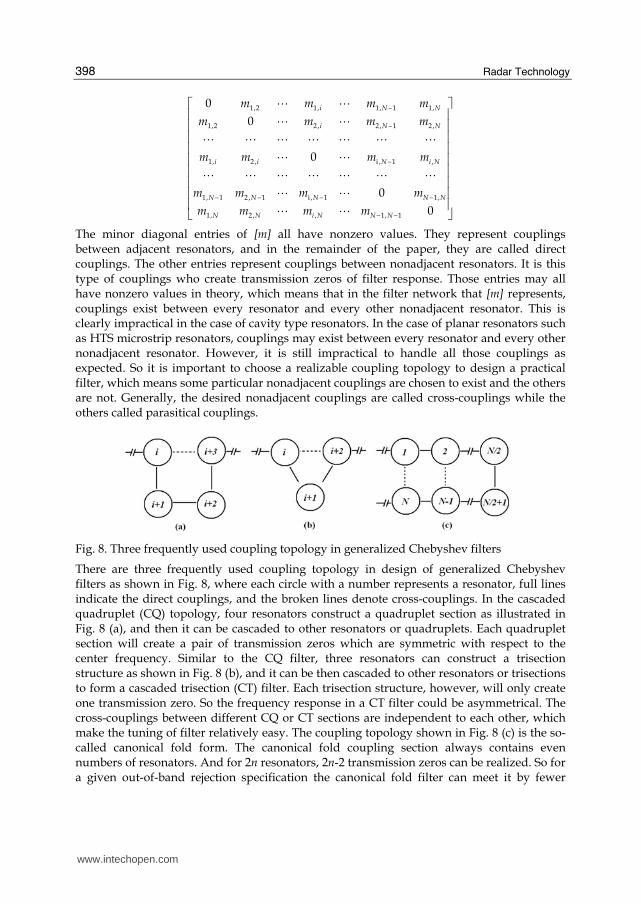
The minor diagonal entries of [m] all have nonzero values. They represent couplings between adjacent resonators, and in the remainder of the paper, they are called direct couplings. The other entries represent couplings between nonadjacent resonators. It is this type of couplings who create transmission zeros of filter response. Those entries may all have nonzero values in theory, which means that in the filter network that [m] represents, couplings exist between every resonator and every other nonadjacent resonator. This is clearly impractical in the case of cavity type resonators. In the case of planar resonators such as HTS microstrip resonators, couplings may exist between every resonator and every other nonadjacent resonator. However, it is still impractical to handle all those couplings as expected. So it is important to choose a realizable coupling topology to design a practical filter, which means some particular nonadjacent couplings are chosen to exist and the others are not. Generally, the desired nonadjacent couplings are called cross-couplings while the others called parasitical couplings.
Fig. 8. Three frequently used coupling topology in generalized Chebyshev filters
There are three frequently used coupling topology in design of generalized Chebyshev filters as shown in Fig. 8, where each circle with a number represents a resonator, full lines indicate the direct couplings, and the broken lines denote cross-couplings. In the cascaded quadruplet (CQ) topology, four resonators construct a quadruplet section as illustrated in Fig. 8 (a), and then it can be cascaded to other resonators or quadruplets. Each quadruplet section will create a pair of transmission zeros which are symmetric with respect to the center frequency. Similar to the CQ filter, three resonators can construct a trisection structure as shown in Fig. 8 (b), and it can be then cascaded to other resonators or trisections to form a cascaded trisection (CT) filter. Each trisection structure, however, will only create one transmission zero. So the frequency response in a CT filter could be asymmetrical. The cross-couplings between different CQ or CT sections are independent to each other, which make the tuning of filter relatively easy. The coupling topology shown in Fig. 8 (c) is the so-called canonical fold form. The canonical fold coupling section always contains even numbers of resonators. And for 2n resonators, 2n-2 transmission zeros can be realized. So for a given out-of-band rejection specification the canonical fold filter can meet it by fewer
www.intechopen.com
Superconducting Receiver Front-End and Its Application In Meteorological Radar
399
resonators than the CQ or CT structure. However, the effect of each cross-coupling in a canonical fold filter is not independent, witch makes the filter tuning more difficult. Once an appropriate coupling topology is determined, the synthesis from characteristic polynomials to coupling matrix may follow the steps of Atia and Williams (Atia & Williams, 1972; Atia et al. 1974). They used the orthonormalization technique to obtain the general coupling matrix with all possible cross-couplings present and repeated similarity transformations are then used to cancel the unwanted couplings to obtain a suitable form of the prototype. Unfortunately, the process does not always converge. In that case optimization technique is a good alternative to derive the sequence of transformations allowing annihilation of the unwanted elements and provide the matrix with the required topology (Chambers & Rhodes 1983; Atia et al., 1998; and Levy, 1995). Generally, the desired couplings in the optimization are evaluated by minimizing a cost function involving the values S11 and S21 at specially selected frequency points such as those transmission and reflection zeros. The entries of the coupling matrix are used as independent variables in the optimization process. The final step in the design of a filter is to find an appropriate resonator and convert the coupling matrix into practical physical structures. Readers can find detailed instructions on how to establish the relationship between the values of every required coupling coefficient and the physical structure of coupled resonators in the book by J. Hong & M. J. Lancaster (Hong & Lancaster, 2001). It is essential in this step to employ helps of computer-aided design (CAD), particularly full-wave electromagnetic (EM) simulation software. EM simulation software solves the Maxwell equations with the boundary conditions imposed upon the RF/microwave structure to be modeled. They can accurately model a wide range of such structures.
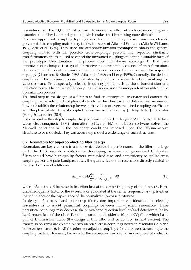
3.2 Resonators for superconducting filter design Resonators are key elements in a filter which decide the performance of the filter in a large
part. The HTS resonators suitable for developing narrow-band generalized Chebyshev
filters should have high-quality factors, minimized size, and conveniency to realize cross
couplings. For a n-pole bandpass filter, the quality factors of resonators directly related to
the insertion loss of a filter as
1
4.343n
CA i
i Ui
L g dBFBW Q=
ΩΔ = ⋅∑ (15)
where ΔLA is the dB increase in insertion loss at the center frequency of the filter, Qui is the
unloaded quality factor of the ith resonator evaluated at the center frequency, and gi is either
the inductance or the capacitance of the normalized lowpass prototype.
In design of narrow band microstrip filters, one important consideration in selecting
resonators is to avoid parasitical couplings between nonadjacient resonators. Those
parasitical couplings may decrease the out-of-band rejection level or/and deteriorate the in-
band return loss of the filter. For demonstration, consider a 10-pole CQ filter which has a
pair of transmission zeros (the design of this filter will be detailed in next section). The
transmission zeros are created by two identical cross-couplings between resonators 2, 5 and
between resonators 6, 9. All the other nonadjacent couplings should be zero according to the
coupling matrix. However, because all the resonators are located in one piece of dielectric
www.intechopen.com

Radar Technology
400
1315.0 1317.5 1320.0 1322.5 1325.0-100
-80
-60
-40
-20
0
M1,10/M1,2=5%
M1,10/M1,2=2.5%
M1,10/M1,2=1%
M1,10/M1,2=0.5%
M1,10/M1,2=0.25%
M1,10/M1,2=0.1%
M1,10/M1,2=0
S21 (
dB
)
Frequency (MHz)
1315.0 1317.5 1320.0 1322.5 1325.0-100
-80
-60
-40
-20
0
S2
1 (
dB
)
Frequency (MHz)
M1,9/M1,2=5%
M1,9/M1,2=2.5%
M1,9/M1,2=1%
M1,9/M1,2=0.5%
M1,9/M1,2=0.25%
M1,9/M1,2=0.1%
M1,9/M1,2=0
(a) (b)
Fig. 9. Illustration of how the parasitical couplings affect the response of a narrow band bandpass filter.
substrate and in one metal housing, parasitical couplings between nonadjacent resonators are inevitable. We have performed a series of analyses by computer simulation on how the parasitical couplings affect the transmission response of this 10-pole CQ filter and the results are plotted in Fig. 9. In Fig.9 (a) different levels of parasitical coupling between resonator 1 and 10 (M1,10) were assumed. It’s magnitude is scaled to the main coupling M1,2. Significant degeneration of the out-of-band rejection level can be seen when M1,10 is higher than 0.1 percent of M1,2. In Fig. 9 (b) the effects of parasitical coupling between resonator 1 and 9 (M1,9) with different strengths were also simulated. It can be seen that in addition to the degeneration of the out-of-band rejection level, the presence of M1,9 also causes the asymmetric transmission response of the filter. To solve these parasitical coupling problems, it is necessary to employ some unique resonators. For example, the hairpin and spiral-in-spiral-out resonators, as depicted in Fig. 6, behave as they have two parallel-coupled microstrips excited in the odd mode when resonating. In this case the currents in these two microstrips are equal and opposite resulting in cancellation of their radiation fields. This characteristic should be of great help in reducing parasitical couplings when design narrow band filters.
3.3 Superconducting filter and receiver front-end subsystem So far the theory and principles for HTS filter design have been discussed generally. In this section the design, construction and integration of a real practical HTS filter and HTS receiver front-end subsystem will be introduced as an application example with one special type of meteorological radar, the wind profiler. The frequencies assigned to the wind profiler are in UHF and L band, which are very crowded and noisy with radio, TV, and mobile communication signals and therefore the radar is often paralyzed by the interference. To solve this problem, it is necessary to employ pre-selective filters. Unfortunately, due to the extremely
narrow bandwidth (≤0.5%) no suitable conventional device is available. The HTS filter can be designed to have very narrow band and very high rejection with very small loss, therefore it is expected that HTS filter can help to improve the anti-interference ability of the wind profiler without even tiny reduction of its sensitivity. In fact, because the low noise amplifier (LNA) in the front end of the receiver is also working at a very low temperature in the HTS subsystem, the sensitivity of the radar will actually be increased.
www.intechopen.com

Superconducting Receiver Front-End and Its Application In Meteorological Radar
401
Fig. 10. Coupling topology of the 10-pole CQ filter designed for the wind profiler.
The center frequency of the wind profiler introduced here is 1320 MHz. In order to reject the near band interference efficiently the filter was expected to have a bandwidth of 5 MHz and skirt slope as sharp as possible. It has been decided in the real design to employ a 10-pole
generalized Chebyshev function filter with a pair of transmission zeros placed at Ω =±1.3 so as to produce a rejection lobe better than 60 dB on both side of the passband. For the implementation of this filter, the CQ coupling topology shown in Fig.10 was employed. The cross couplings M2,5 and M6,9 in Fig.10 are introduced to create the desired transmission zeros. In the present design they are set to be equal to each other to create the same pair of transmission zeros. Introducing two identical cross couplings can make the physical structure of the filter symmetric. With this strictly symmetric physical structure, only half part (e.g., the left half) of the whole filter is needed to be simulated in the EM simulation process, which will simplify the EM simulation and save the computing time remarkably. The transfer and reflection functions and the coupling matrix can then be synthesized following the instructions in section 3.1. For this filter with topologic structure shown in Fig. 10, the finally coupling parameters are: Qe1= Qe2=237.3812, and
0 0.330 0 0 0 0 0 0 0 0
0.330 0 0.218 0 0.0615 0 0 0 0 0
0 0.218 0 0.262 0 0 0 0 0 0
0 0 0.262 0 0.188 0 0 0 0 0
0 0.0615 0 0.188 0 0.198 0 0 0 00.01
0 0 0 0 0.198 0 0.188 0 0.0615 0
0 0 0 0 0 0.188 0 0.262 0 0
0 0 0 0 0 0 0.262 0 0.218 0
0 0 0 0 0 0.0615 0 0.218 0 0.330
0 0 0 0 0 0 0 0 0.330 0
M
⎡
= ×
⎤⎢ ⎥⎢ ⎥⎢ ⎥⎢ ⎥⎢ ⎥⎢ ⎥⎢ ⎥⎢ ⎥⎢ ⎥⎢ ⎥⎢ ⎥⎢ ⎥⎢ ⎥⎢ ⎥⎣ ⎦
The synthesized response of the filter is depicted in Fig.11. The designed filter shows a symmetric response which gives a rejection lobe of more than 60 dB on both side of the passband as expected. The passband return loss is 22 dB and the band width is 5 MHz centered at 1320 MHz. Two transmission zeros locate at 1316.75 MHz and 1320.25 MHz respectively. The resonator used in this filter is spiral-in-spiral-out type resonator as shown in Fig.12 (a), which is slightly different from that shown in Fig.6 (f). The main change is that both end of the microstrip line are embedded into the resonator to form capacitance loading, making the electric-magnetic field further constrained. More over the middle part of the microstrip line where carries the highest currents at resonance was widened to increase the quality factor of
www.intechopen.com
Radar Technology
402
1310 1315 1320 1325 1330-100
-80
-60
-40
-20
0 synthesized
Simulated
Ma
gn
etitu
de (
dB
)
Frequency (MHz)
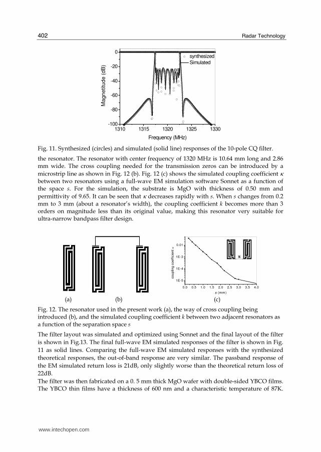
Fig. 11. Synthesized (circles) and simulated (solid line) responses of the 10-pole CQ filter.
the resonator. The resonator with center frequency of 1320 MHz is 10.64 mm long and 2.86 mm wide. The cross coupling needed for the transmission zeros can be introduced by a
microstrip line as shown in Fig. 12 (b). Fig. 12 (c) shows the simulated coupling coefficient κ between two resonators using a full-wave EM simulation software Sonnet as a function of the space s. For the simulation, the substrate is MgO with thickness of 0.50 mm and
permittivity of 9.65. It can be seen that κ decreases rapidly with s. When s changes from 0.2 mm to 3 mm (about a resonator’s width), the coupling coefficient k becomes more than 3 orders on magnitude less than its original value, making this resonator very suitable for ultra-narrow bandpass filter design.
0.0 0.5 1.0 1.5 2.0 2.5 3.0 3.5 4.0
1E-5
1E-4
1E-3
0.01
co
uplin
g c
oe
ffic
ien
t κ
s (mm) (a) (b) (c)
Fig. 12. The resonator used in the present work (a), the way of cross coupling being introduced (b), and the simulated coupling coefficient k between two adjacent resonators as a function of the separation space s
The filter layout was simulated and optimized using Sonnet and the final layout of the filter
is shown in Fig.13. The final full-wave EM simulated responses of the filter is shown in Fig.
11 as solid lines. Comparing the full-wave EM simulated responses with the synthesized
theoretical responses, the out-of-band response are very similar. The passband response of
the EM simulated return loss is 21dB, only slightly worse than the theoretical return loss of
22dB.
The filter was then fabricated on a 0. 5 mm thick MgO wafer with double-sided YBCO films. The YBCO thin films have a thickness of 600 nm and a characteristic temperature of 87K.
www.intechopen.com

Superconducting Receiver Front-End and Its Application In Meteorological Radar
403
Fig. 13. The final layout of the 10-pole quasi-elliptic filter (not to scale).
Both sides of the wafer are gold-plated with 200 nm thick gold (Au) for the RF contacts. The
whole dimension of the filter is 60 mm×30 mm×20 mm including the brass housing. The RF measurement was made using a HP 8510C network analyzer and in a cryogenic cooler. Fig.14 shows the measured results at 70K and after tuning the filter. The measured center frequency is 1.319 GHz, and the return loss in the passband is better than 15 dB. The insertion loss at the passband center is 0.26 dB, which corresponds to a filter Q of about 45,000. The transmission response is very similar to the theoretically synthesized and the full-wave EM simulated responses as shown in Fig. 11. The fly-back values in the S21 curve are 60.7 dB and 62 dB at the lower and upper frequency sides, respectively. Steep rejection slopes at the band edges are obtained and rejections reach more than 60 dB in about 500 kHz from the lower and upper passband edges.
1.310 1.315 1.320 1.325 1.330-100
-80
-60
-40
-20
0
-50
-40
-30
-20
-10
0
S2
1 (
dB
)
Frequency (GHz)
S1
1 (
dB
)
Fig. 14. The measured response of the 10-pole filter at 70K
Combining this filter together with a low noise amplifier (LNA) as well as a Sterling cryo-cooler, a HTS subsystem was then constructed as shown schematically in Fig. 15 (a). There are many types of cryo-coolers in the market which are specially built for a long life under outdoor conditions in order to provide high cooling power at a cryogenic temperature. What we chose for the HTS wind profiler subsystem is Model K535 made by Ricor Cryogenic & Vacuum Systems, Israel, for its considerably compact volume and longer life time (Fig. 15 (b)). The advantage of integrating the LNA together with HTS filter inside the cryo-cooler is obvious, as the noise figure of LNA is temperature dependent (Fig. 16 (a)).
www.intechopen.com

Radar Technology
404
Since the cost of a cryo-cooler is inevitable for HTS filters. Extra benefit of significant reduction of noise figure can be obtained by also putting the LNA in low temperature without any new burden of cooling devices. The noise figure of the HTS receiver front-end subsystem measured using an Agilent N8973A Noise Figure Analyzer at 65 K is about 0.7 dB in major part (80%) of the whole passband, as shown in Fig. 16 (b).
(a) (b)
Fig. 15. Sketch and photograph of the HTS receiver front-end subsystem
(a) (b)
Fig.16. Temperature dependence of the noise figure of the LNA used in the HTS subsystem (a) and the noise figure of the HTS front-end subsystem measured at 70K (b)
4. Superconducting meteorological radar
4.1 Basic principle and configuration of wind profiler A wind profiler is a type of meteorological radar that uses radar to measure vertical profiles of the wind, i.e., detecting the wind speed and direction at various elevations above the ground. The profile data is very useful to meteorological forecasting and air quality monitoring for flight planning. Pulse-Doppler radar is often used in wind profiler. In a typical profiler, the radar can sample along each of three beams: one is aimed vertically to measure vertical velocity, and two are tilted off vertical and oriented orthogonal to one another to measure the horizontal components of the air's motion. The radar transmits an electromagnetic pulse along
www.intechopen.com

Superconducting Receiver Front-End and Its Application In Meteorological Radar
405
each of the antenna's pointing directions. Small amounts of the transmitted energy are scattered back and received by the radar. Delays of fixed intervals are built into the data processing system so that the radar receives scattered energy from discrete altitudes, referred to as range gates. The Doppler frequency shift of the backscattered energy is determined, and then used to calculate the velocity of the air toward or away from the radar along each beam as a function of altitude. The photograph of a typical wind profiler is shown in Fig. 17. Two antennas can be clearly seen in the middle of the photograph, one is vertical and the other is tilted. The third antenna is hidden by one of the four big columns, which are used for temperature profile detection by sound waves (SODAR). The circuit diagram of a typical wind profiler is shown in Fig 18. The “transmitting system” transmits pulse signal through the antenna, then the echoes come back through the LNA to the “radar receiving system”, that analyzes the signal and produces wind profiles.
Fig. 17. Photograph of a typical wind profiler
The wind profiler measures the wind of the sky above the radar site in three directions, i.e.,
the roof direction, east/west direction and south/north direction, and produces the wind
charts correspondingly. The collected wind chart data are then averaged and analyzed at
every 6 minutes so as to produce the wind profiles. Typical wind profiles are shown in Fig.
19 (a). In the profile the horizontal axis denotes the time (starting from 5:42 AM to 8:00 AM
with intervals of every 6 minutes); the vertical axis denotes the height of the sky. The arrow-
like symbols denote the direction and velocity of the wind at the corresponding height and
in corresponding time interval. The arrowhead denotes the wind direction (according to the
provision: up-north, down-south, left-west, right-east), and the number of the arrow feather
denotes the wind velocity (please refer to the legend).
Fig. 18. Circuit diagram of a typical wind profiler.
www.intechopen.com

www.intechopen.com

www.intechopen.com

Radar Technology
408
4.3 Field trail of superconducting meteorological radar As already mentioned the wind profiler measures the wind of the sky above the radar site in three directions and produces the wind charts correspondingly. A typical wind chart of the east/west direction is presented in Fig. 21, where the horizontal axis is the wind velocity (m/s, corresponding to the frequency shift due to the Doppler effect) and the vertical axis is the height of the sky above the radar site (from 580 m to 3460 m with intervals of every 120 m) corresponding to the time when different echo being received. The negative values of the wind velocity indicate the change in wind direction. Each curve in Fig 21 represents the spectrum of corresponding echo. The radar system measures the wind charts of the sky above every 40 seconds. The collected wind chart data are then averaged and analyzed at every 6 minutes so as to produce the wind profiles. The procedure of the second stage experiments (field trail) is as follows: firstly, the wind charts and the wind profiles were measured using the conventional wind profiler without any interference signal. Then an interference signal with a frequency of 1322.5 MHz and power of -4.5 dBm was applied and a new set of wind charts and wind profiles being obtained. Finally, the wind charts and the wind profiles were measured using the HTS wind profiler (the LNA at the front end of the conventional wind profiler being replaced by the HTS subsystem) with the same frequency but much stronger (+10 dBm) interference signal. It can be seen that a series of interference peaks appeared in the wind chart measured using the conventional wind profiler while the interference signal was introduced (Fig. 21 (b)). However, no influence of the interference can be seen at all in the wind charts produced by the HTS wind profiler (Fig. 21 (c)), even when much stronger (up to +10 dBm) interference signal being applied. Moreover, the ultimate height of the wind in the sky being able to be detected reaches to 4000 meters when HTS subsystem was used (Fig. 21 (c)), in contrast with those of 3400 meters of conventional ones (Fig. 21 (a) and (b)), which is consistent with the picture that sensitivity of the HTS radar system is higher than that of the conventional system.
(a) (b) (c)
Fig. 21. Wind charts produced by (a) using the conventional wind profiler without interference, (b) using the conventional wind profiler with interference (1322.5 MHz, -4.5 dBm), (c) using the HTS wind profiler with interference (1322.5 MHz, +10 dBm)
Fig. 22 shows the wind profiles produced from the wind charts measured in the same day by the conventional wind profiler and the HTS wind profiler, respectively. It can be clearly seen that the conventional wind profiler cannot attain wind profiles above 2000 m due to the influence of the interference signal, which reproduced the phenomena observed in Fig 19.
www.intechopen.com

Superconducting Receiver Front-End and Its Application In Meteorological Radar
409
On the contrary the HTS wind profiler functioned well even with much serious interference signal.
Fig. 22. Wind profiles obtained under three different conditions by the conventional wind profiler and the HTS wind profiler, respectively
5. Summary
Due to the atrocious electromagnetic environment in UHF and L band, high performance pre-selective filters are requested by the meteorological radar systems, e.g. the wind
profilers. Unfortunately, due to the extremely narrow bandwidth (≤0.5%) no conventional device is available. To solve this problem, an ultra selective narrow bandpass 10-pole HTS filter has been successfully designed and constructed. Combining this filter together with a low noise amplifier (LNA) as well as a cryocooler, a HTS receiver front-end subsystem was then constructed and mounted in the front end of the receiver of the wind profiler. Quantitative comparison experiments demonstrated that with this HTS subsystem an increase of 3.7 dB in the sensitivity and an improvement of 48.4 dB in the ability of interference rejection of the radar were achieved. Field tests of this HTS wind profiler showed clearly that when conventional wind profiler failed to detect the velocity and direction of the wind above 2000 meters in the sky of the radar site due to interference, the HTS wind profiler can produce perfect and accurate wind charts and profiles. A demonstration HTS wind profiler is being built and will be installed in a weather station in the suburb of Beijing. Results of this HTS radar will be reported in due course.
6. References
Amari, S. (2000). Synthesis of Cross-Coupled Resonator Filters Using an Analytical Gradient-Based Optimization Technique, IEEE Trans. Microwave Theory and Techniques, Vol. 48, No.9, pp.1559-1564
Atia, A. E. & Williams, A. E. (1972). Narrow-bandpass waveguide filters, IEEE Trans. Microwave Theory and Techniques, Vol. 20, No.4, pp.258-264
www.intechopen.com
Radar Technology
410
Atia, A. E.; Williams, A. E. & Newcomb, R. W. (1974). Narrow-band multiple-coupled cavity synthesis, IEEE Trans. Microwave Theory and Techniques, Vol. 21, No.5, pp.649-656
Atia, A. W., Zaki, K. A. & Atia, A. E. (1998). Synthesis of general topology multiple coupled resonator filters by optimization, IEEE MTT-S Digest, Vol. 2, pp. 821-824
Bednorz, J. G. & Mueller, K. A. (1986). Possible high Tc superconductivity in the Ba-La-Cu-O system, Z. fur Phys. Vol. 64, pp. 189-192
Cameron, R. J. (1999). General coupling matrix synthesis methods for Chebyshev filtering functions, IEEE Trans .Microwave Theory and Techniques, Vol. 47, No.4, pp.433-442
Cameron, R. J. & Rhodes, J. D. (1981). Asymmetric realizations for dual-mode bandpass filters, IEEE Trans. Microwave Theory and Techniques, Vol. 29, No.1, pp.51-59
Chambers, D. S. G. & Rhodes, J. D. (1983). A low-pass prototype network allowing the placing of integrated poles at real frequencies, IEEE Trans. Microwave Theory and Techniques, Vol. 33, No.1, pp.40-45
Gorter, C. J. & Casimir, H. B. (1934). On superconductivity I, Physica, Vol. 1, 306 Hong, J.-S. & Lancaster, M. J. (2001). Microstrip filters for RF/microwave applications, John
Wiley & Sons, Inc., ISBN 0-471-38877-7 New York Hong, J. S.; Lancaster, M. J.; Jedamzik, D. & Greed, R. B. (1999). On the development of
superconducting microstrip filters for mobile communications applications, IEEE Trans on Microwave Theory and Techniques , Vol. 47, pp. 1656-1663
Kammerlingh Onnes, H. (1911). The resistance of pure mercury at helium temperature, Commun. Phys. Lab. Uni. Leiden, 120b. 3
Lancaster, M. J. (1997). Passive Microwave devices applications of high temperature superconductors, Cambridge University Press, ISBN 0-521-48032-9, Cambridge
Levy, R. (1995). Direct synthesis of cascaded quadruplet (CQ) filters, IEEE Trans. Microwave Theory and Techniques, Vol. 43, No.12, pp.2940-2945
Li, H.; He, A. S.& He, Y. S. et al. (2002). HTS cavity and low phase noise oscillator for radar
application,IEICE transactions on Electronics,Vol. E85-C,No.3,pp. 700-703
Li, Y. Lancaster, M. J. & Huang, F. et al (2003). Superconducting microstrip wide band filter for radio astronomy, IEEE MTT-S Digest, pp. 551-553
Lyons W. G.; Arsenault, D. A. & Anderson, A. C. et al. (1996). High temperature superconductive wideband compressive receivers, IEEE Trans. on Microwave Theory and Techniques, Vol. 44, pp. 1258-1278
Macchiarella, G. (2002). Accurate synthesis of inline prototype filters using cascaded triplet and quadruplet sections, IEEE Trans. Microwave Theory and Techniques, Vol. 50, No.7, pp.1779-1783
Meissner, W. & Ochsenfeld, R. (1933). Naturwissenschaften, Vol. 21,pp.787-788 Romanofsky, R. R.; Warner, J. D. & Alterovitz, S. A. et al. (2000). A Cryogenic K-Band
Ground Terminal for NASA’S Direct-Data-Distribution Space Experiment, IEEE Trans. on Microwave Theory and Techniques, Vol.. 48, No. 7, pp. 1216-1220
STI Inc. (1996). A receiver front end for wireless base stations, Microwave Journal, April 1966, 116.
Wallage, S.; Tauritz, J. L. & Tan, G. H. et al (1997). High-Tc superconducting CPW band stop filters for radio astronomy front end. IEEE Trans. on Applied Superconductivity, Vol. 7 No. 2, pp. 3489-3491.
Zhang, Q.; Li, C. G. & He, Y. S. et al (2007). A HTS Bandpass Filter for a Meteorological Radar System and Its Field Tests, IEEE Transactions on Applied Superconductivity, Vol. 17, No2, pp. 922-925
www.intechopen.com

Radar TechnologyEdited by Guy Kouemou
ISBN 978-953-307-029-2Hard cover, 410 pagesPublisher InTechPublished online 01, January, 2010Published in print edition January, 2010
InTech EuropeUniversity Campus STeP Ri Slavka Krautzeka 83/A 51000 Rijeka, Croatia Phone: +385 (51) 770 447 Fax: +385 (51) 686 166www.intechopen.com
InTech ChinaUnit 405, Office Block, Hotel Equatorial Shanghai No.65, Yan An Road (West), Shanghai, 200040, China
Phone: +86-21-62489820 Fax: +86-21-62489821
In this book “Radar Technology”, the chapters are divided into four main topic areas: Topic area 1: “RadarSystems” consists of chapters which treat whole radar systems, environment and target functional chain. Topicarea 2: “Radar Applications” shows various applications of radar systems, including meteorological radars,ground penetrating radars and glaciology. Topic area 3: “Radar Functional Chain and Signal Processing”describes several aspects of the radar signal processing. From parameter extraction, target detection overtracking and classification technologies. Topic area 4: “Radar Subsystems and Components” consists ofdesign technology of radar subsystem components like antenna design or waveform design.
How to referenceIn order to correctly reference this scholarly work, feel free to copy and paste the following:
Yusheng He and Chunguang Li (2010). Superconducting Receiver Front-End and Its Application InMeteorological Radar, Radar Technology, Guy Kouemou (Ed.), ISBN: 978-953-307-029-2, InTech, Availablefrom: http://www.intechopen.com/books/radar-technology/superconducting-receiver-front-end-and-its-application-in-meteorological-radar

© 2010 The Author(s). Licensee IntechOpen. This chapter is distributedunder the terms of the Creative Commons Attribution-NonCommercial-ShareAlike-3.0 License, which permits use, distribution and reproduction fornon-commercial purposes, provided the original is properly cited andderivative works building on this content are distributed under the samelicense.