supercapacitor backup power supply w/ current limit for
TRANSCRIPT

Application ReportSmart Electricity Meter Supercapacitor Backup Power Supply With Current Limit
Andrew Soukup, Florian Mueller, Julian Hagedorn
ABSTRACT
A reference design for a backup power supply for smart electricity meters is implemented with a low-power Buck-Boost converter that both charges and regulates the output of a dual supercapacitor array, which simplifies and lowers overall cost. The design provides output current up to 2 A for meters high-power RF communications, and an adjustable charge limit to reduce system heating concerns.
Table of Contents1 System Description................................................................................................................................................................ 22 System Overview.................................................................................................................................................................... 33 Test Results...........................................................................................................................................................................124 References............................................................................................................................................................................ 155 Revision History................................................................................................................................................................... 15
List of FiguresFigure 2-1. PMP30693 Block Diagram........................................................................................................................................ 3Figure 2-2. TPS63802 Functional Block Diagram....................................................................................................................... 5Figure 2-3. LM66100 Functional Block Diagram......................................................................................................................... 5Figure 2-4. Power ORing with LM66100......................................................................................................................................6Figure 2-5. Simplified Block Diagram of PMP30693....................................................................................................................6Figure 2-6. Peak Current Operation, Reverse Current................................................................................................................ 7Figure 2-7. General Implementation to Stop Charging the Backup Capacitor.............................................................................7Figure 2-8. Backup Capacitor Voltage in Steady State................................................................................................................8Figure 2-9. Schematic Implementation of the Supercapacitor Voltage Supervisor......................................................................8Figure 2-10. Simplified Schematic Implementation of Current Limiting Circuit............................................................................9Figure 2-11. Typical GSM Load Profile for Backup Time Calculation........................................................................................ 10Figure 2-12. Implementation of Automatic PFM Mode Change During Backup Operation....................................................... 10Figure 2-13. Active Cell Balancing Implementation................................................................................................................... 11Figure 2-14. Output Voltage Adjustment Implementation.......................................................................................................... 11Figure 3-1. Simplified Block Diagram of PMP30693..................................................................................................................12Figure 3-2. Pre-Charging and Charging of the Backup Capacitor............................................................................................. 13Figure 3-3. Backup Operation....................................................................................................................................................13Figure 3-4. Normal Steady-State Operation.............................................................................................................................. 14
List of TablesTable 2-1. PMP30693 Reference Design Specifications............................................................................................................. 4
TrademarksAll trademarks are the property of their respective owners.
www.ti.com Table of Contents
SLVAEI4A – OCTOBER 2019 – REVISED AUGUST 2021Submit Document Feedback
Smart Electricity Meter Supercapacitor Backup Power Supply With Current Limit
1
Copyright © 2021 Texas Instruments Incorporated

1 System DescriptionReliability and rapid recovery from grid outages are fundamental requirements of the Smart Grid. Smart electricity meters with Advanced Metering Infrastructure (AMI) networks must be able to continue operating for a short time in the absence of mains power in order to alert utility operators that an outage has occurred, and provide a clear map of how widespread the service interruption truly is. This allows the operator to diagnose the root cause, deploy resources and personnel to repair the issue, and restore service to consumers as rapidly as possible.
This system requirement poses a design challenge to smart electricity meter developers. The meter must have sufficient local energy storage to energize the AMI network for a period long enough that all meter end points can report their status to the utility’s central office; this can take several minutes depending on the geographical and network topology involved.
When considering the common case of an AMI network that implements a Radio Frequency (RF) mesh topology, where each meter node can act as a bridge back to the central office for any other node, the requirement becomes clear. In order to ensure that any node which has lost power is able to report the outage, every other node must stand ready to act as a bridge and ‘hop’ the outage notification to the data concentrator head-end system or to the next node in the mesh. Therefore, all meter nodes must be fully operational during this period after an outage.
In order to support this requirement, smart electricity meters typically use super capacitors to store the required energy. Super capacitors provide good energy density per cm3, and are easily recharged once mains power is restored, making them a popular choice compared to batteries.
Smart meter developers must balance the required amount of energy available to the system during an outage versus the system cost of the super capacitor and its required charging and output regulation circuitry. The key to this balance is maximizing the amount of usable energy extracted from each supercapacitor.
This application report details a proposed architecture for the electricity meter backup power supply using a low-power Buck-Boost converter to both manage the supercapacitor charging and provide the maximum energy available to the system. This application note is a companion document to the PMP30693 reference design.
System Description www.ti.com
2 Smart Electricity Meter Supercapacitor Backup Power Supply With Current Limit
SLVAEI4A – OCTOBER 2019 – REVISED AUGUST 2021Submit Document Feedback
Copyright © 2021 Texas Instruments Incorporated

2 System OverviewThe backup power supply system diagram is shown in Figure 2-1. The TPS63802 low-power buck-boost converter functions as both the supercapacitor charger and, as the output voltage regulator, which supplies energy to the wireless communications subsystem. The LM66100 ideal diode provides reverse blocking protection during supercapacitor discharge. The benefits of the proposed backup power supply architecture include:
• Reduced system cost through elimination of separate supercapacitor charging circuitry.• Support for public carrier cellular modems such as LTE/3G/GPRS or private ISM-band communication
networks due to output voltage of up to 5 V with peak output current of 2 A at 3.3 V.• The supercapacitor can be charged at higher than the main supply rail, which raises the amount of backup
energy available.• Seamless transition between charging mode and discharge mode in the case of an outage ensure rapid
switchover to backup power without interruption.• Programmable limits to the charge current are available as an optional feature.• Active cell balancing for 2S super capacitor arrays is available as an optional feature.
2.1 Block Diagram
TPS63802
LX1 LX2
VIN VOUT
PGND
L1
FB
MODE
EN
AGND
+
±
PG
EDLC
+
±
V(SYS)
LM66100
LM66100
+
±
System Supply
(not part of
Reference Design)
Optional if current limit
for charging is needed
Power OR ing
V(SYS)
(Mode)
Backup+
±
Optional if active cell
balancing is needed
Optional if automatic
PFM mode selection is
needed for discharge
Optional, place load switch or ideal
diode, to disable Precharge path
VSEL
V(MAIN)
V(CAP)
Figure 2-1. PMP30693 Block Diagram
2.2 Design ConsiderationsThis design provides an efficient method to extract maximum energy from a supercapacitor, and provides the required voltage and current to the RF subsystem. GPRS or GSM systems need peak currents of up to 2 A for several 100 us. LTE transmissions require peak currents of up to 1 A. That energy needs to be provided by the mains supply during normal operation. If the mains supply is not able to supply the needed peak currents, or fails completely, the backup power supply system jumps in.
The chosen TPS63802 is capable of providing >2 A over a wide input voltage range from the supercapacitors. The transition between mains supply and the backup supply happens automatically and seamlessly. When the system voltage drops under a certain threshold, which is usually 100 mV lower than the system voltage, the buck-boost converter starts switching. The required energy is transferred from the supercapacitors to the system.
www.ti.com System Overview
SLVAEI4A – OCTOBER 2019 – REVISED AUGUST 2021Submit Document Feedback
Smart Electricity Meter Supercapacitor Backup Power Supply With Current Limit
3
Copyright © 2021 Texas Instruments Incorporated

The TPS63802 buck-boost converter does have a defined reverse peak current limit of -900 mA, which results in an average charging current of around 1.2 A. However, if a mains supply is not able to provide enough current for the system and the charging of the supercapacitor, the charging current needs to be limited. Such a mains supply could be, for example, the TPS7A78 AC/DC linear voltage regulator. The PMP30693 reference design also includes an optional circuit based on INA181 to limit the charging current minimum of 50 mA.
The reverse current operation of the buck-boost converter allows boosting up the supercapacitor voltage above the mains supply. This fact, in combination with the low input voltage of 1.3 V, means the TPS63802 uses most of the energy stored in the supercapacitor.
This reference design follows the following specifications, see Table 2-1.
Table 2-1. PMP30693 Reference Design SpecificationsParameter Spec Units CommentsV(MAIN) 0 to 5, 3.9 typ V In backup case, this is 0 V. Here,
the system supply is 3.9 V.
V(SYS) 3.3 to 5V, 3.9V typ V
V(CAP) 0 to 5.4 V Here limited to 5 V, when charged.
V(BACKUP) 3.8 typ V TPS63802 programmed output voltage need to be slightly below V(MAIN) to allow charging.
Capacitance 12.5 F 2x 25F in series.
Backup time >100 s With pulsed load profile.
Cap precharge current 50 typ mA Configurable through resistor.
Cap charge current, limited >-50 mA Limited capacitor charge current.
Cap charge current, max (unlimited)
-900 mA, peak Average current is approximately 1.1A.
Cap discharge current, max 2.0 A
Load profile at V(SYS) 311 mA avg GSM load profile.
V(SYS) Output voltage Drop 200 mV max In backup case.
2.3 Highlighted ProductsThe PMP30693 design includes the TPS63802, a high-efficiency, low Iq, bidirectional buck-boost DC/DC converter that charges a super capacitor up to 5.4 V and discharges it down to 1.3 V. The LM66100 ideal diode is used for reverse current blocking and power Oring between main system supply and backup power from the supercapacitor. The low-cost INA181 is used to control and limit the supercapacitor charging current, while the low-cost operational amplifier TLV52x is used as a voltage supervisor and in the active cell balancing.
2.3.1 TPS63802: 2-A Output Current, High-Efficient, Low IQ Buck-Boost Converter
The TPS63802 device is used when the input voltage is higher, equal, or lower than the output voltage. Output currents up to 2 A are supported over a wide voltage range. The device limits the peak current at 4.5 A in boost-mode and 3.5 A in buck-mode. The device is adjusted to the programmed output voltage. The TPS63802 device comes in a 2 mm × 3 mm package. The device works with tiny passive components to keep the overall solution size small. The TPS63802 buck-boost converter uses four internal switches to maintain synchronous power conversion at all possible operating conditions.
System Overview www.ti.com
4 Smart Electricity Meter Supercapacitor Backup Power Supply With Current Limit
SLVAEI4A – OCTOBER 2019 – REVISED AUGUST 2021Submit Document Feedback
Copyright © 2021 Texas Instruments Incorporated

Gate
Driver
Current
Sensor
+
±
Gate
Driver
CIN
Device Control
Power Safe Mode
Protection
Current Limit
Buck/Boost Control
Off-time calculation
Soft-Start
VMAX SwitchVINVOUT
+
±
VIN
Device
Control
Device
Control
COUT
EN
MODE
GND
+
± Ref
500 mV
Device
Control
L1 L2
L
VIN
VOUT
L1, L2
Gate
Driver
Power
Good
Ref
1.1 V
VOUT
PG
FB
AGND
Figure 2-2. TPS63802 Functional Block Diagram
This enables the device to keep high efficiency over a wide input-voltage and output-load range. To regulate the output voltage at all possible input voltage conditions, the device automatically transits between buck, buck-boost, and boost operation as required by the configuration. In buck and boost modes, it always uses one active switch, one rectifying switch, one switch on, and one switch held off. It remains in a three-cycle buck-boost mode when the input voltage is approximately equal to the output voltage. The transitions happen seamlessly and avoid unwanted toggling within the modes.
2.3.2 LM66100
The LM66100 is a Single-Input, Single-Output (SISO) integrated ideal diode that is well-suited for a variety of applications. The device contains a P-channel MOSFET that can operate over an input voltage range of 1.5 V to 5.5 V and can support a maximum continuous current of 1.5 A.
CL RLON
OFF
RST
STLogic+
±
CE
ON
OFF
VIN
+
±VIN
VIN VOUT
Figure 2-3. LM66100 Functional Block Diagram
Two LM66100 devices can be used in an ORing configuration similar to a dual-diode ORing implementation. In this configuration, the devices pass the highest input voltage to the output while blocking reverse current flow into the input supplies. These devices can compare input and output voltages to make sure that reverse current is blocked through an internal voltage comparator.
www.ti.com System Overview
SLVAEI4A – OCTOBER 2019 – REVISED AUGUST 2021Submit Document Feedback
Smart Electricity Meter Supercapacitor Backup Power Supply With Current Limit
5
Copyright © 2021 Texas Instruments Incorporated
CL RL
ST
Logic+
±
CE
VIN1+
±
VIN VOUT
ST
Logic+
±
CE
+
±
VIN
Status
Indication
Status
Indication
VIN2
GND
GND
Figure 2-4. Power ORing with LM66100
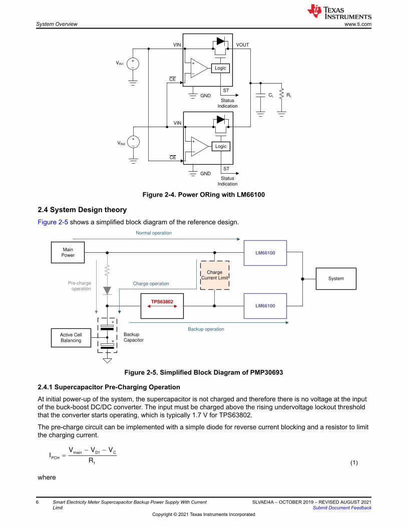
2.4 System Design theoryFigure 2-5 shows a simplified block diagram of the reference design.
+
Backup
Capacitor
System
Normal operation
Charge operation
Main
Power
System
TPS63802
Active Cell
Balancing +
Backup operation
Pre-charge
operation
LM66100
LM66100
Charge
Current Limit
Figure 2-5. Simplified Block Diagram of PMP30693
2.4.1 Supercapacitor Pre-Charging Operation
At initial power-up of the system, the supercapacitor is not charged and therefore there is no voltage at the input of the buck-boost DC/DC converter. The input must be charged above the rising undervoltage lockout threshold that the converter starts operating, which is typically 1.7 V for TPS63802.
The pre-charge circuit can be implemented with a simple diode for reverse current blocking and a resistor to limit the charging current.
main D1 C
PCH
1
V V VI
R
� �
(1)
where
System Overview www.ti.com
6 Smart Electricity Meter Supercapacitor Backup Power Supply With Current Limit
SLVAEI4A – OCTOBER 2019 – REVISED AUGUST 2021Submit Document Feedback
Copyright © 2021 Texas Instruments Incorporated

• VMain: Main power voltage• VD1: Forward voltage of diode D1• VC: Backup capacitor voltage• R1: Resistor to set the pre-charging current• IPCH: Pre-charge current
2.4.2 Supercapacitor Charging Operation with Current Limit
Most buck-boost DC/DC converters allow the device current to flow in reverse direction. This happens due to the negative current capability of these devices. The typical negative peak current target is set to 0.9 A for TPS63802. Even though the target has a negative value, the average current is even more negative than the peak current.
0time
IPEAK
IIND
IPK-PK
IAVG
VEAmp
Figure 2-6. Peak Current Operation, Reverse Current
In order to allow reverse current to flow, two conditions need to be true. First, the output voltage target must be a bit lower than the applied output voltage.
4
OUT FB
5
RV 1 V
R
§ · � u¨ ¸¨ ¸© ¹ (2)
where
• VOUT: Programmed output voltage of the TPS63802• VFB: Feedback voltage of TPS63802 (500 mV typical)• R4, R5: Resistors of the output voltage divider
Second, the converter needs to be forced to PWM mode that it is constantly switching. In the TPS63802, the MODE pin needs to be pulled to VIN.
If both conditions are true, the converter tries to adjust the output voltage by sinking current. This current charges the supercapacitor on the input side until the input overvoltage protection feature triggers, which in the TPS63802 is typically at 5.7 V.
For a two-cell supercapacitor design, the maximum voltage is typically 5.4 V. Therefore, an external voltage monitoring circuit needs to be implemented to stop charging. The charging can be stopped by changing the operating mode from forced PWM to PFM mode. This design uses a simple resistor divider and an operational amplifier (TLV522).
+
+
Backup
Capacitor
R2
R3+
±
VTH
VREF
VPS
Vin
MODE
TPS63802
Figure 2-7. General Implementation to Stop Charging the Backup Capacitor
www.ti.com System Overview
SLVAEI4A – OCTOBER 2019 – REVISED AUGUST 2021Submit Document Feedback
Smart Electricity Meter Supercapacitor Backup Power Supply With Current Limit
7
Copyright © 2021 Texas Instruments Incorporated

Due to the leakage current of the backup capacitor, the quiescent current of the TPS63802 and the current through the resistor divider (R2 , R3), the supercapacitor is slowly discharged. When the voltage VTH falls below the falling threshold of the comparator, it changes the MODE pin back to forced PWM to charge the supercapacitor again. Figure 2-4 shows the voltage at the charged supercapacitor in steady state operation.
VCR
VCF
Figure 2-8. Backup Capacitor Voltage in Steady State
In this design the supercapacitor voltage supervisor is implemented with a simple operational amplifier, the TLV522. Since the TLV522 does not have an internal reference, the TLV431 is used to generate a 1.25-V reference.
EDLC
+
±
VIN
MODE
EN
GND
VSUP
RSUP
R1
0.1%
R2
0.1%
CATHODE
TL431
ANODE
Figure 2-9. Schematic Implementation of the Supercapacitor Voltage Supervisor
The system designer may choose to charge the supercapacitor at less than the full 1.2A capability of the TPS63802 for several reasons such as limiting the cost of the main system supply or reducing heat buildup and the need to dissipate it. PMP30693 includes a charge current limiter feature for this purpose.
The INA181 current sense amplifier is used to measure the voltage across the sense resistor and outputs a control voltage. This voltage is connected through a resistor to the feedback pin. It adjusts the feedback voltage such that the converter stops charging. This limits the current on average.
System Overview www.ti.com
8 Smart Electricity Meter Supercapacitor Backup Power Supply With Current Limit
SLVAEI4A – OCTOBER 2019 – REVISED AUGUST 2021Submit Document Feedback
Copyright © 2021 Texas Instruments Incorporated

+
±
Rsense
ref
Vout Pin
FB pin
R1
GND
R2R3
TPS63802
0.5 V
Vout
VoutMain Power
INA181
Figure 2-10. Simplified Schematic Implementation of Current Limiting Circuit
This reference design is able to limit the charging current down to 50 mA.
out FB INA FB FB
1 3 2
V V V V V
R R R
� �
�
(3)
where
• VINA=IcurrLim× Rsense• Vout: output voltage during charging• VFB: TP63802 feedback voltage
The current limit can be calculated with this formula:
� �FB 1 3 2 3 1 2 out 2 3
currLim
1 2 sense
V R R R R R R V R RI
R R R
u � u � u � u u
u u (4)
2.4.3 Backup Operation
In case of power loss of the mains supply, the buck-boost converter supplies the system. The system voltage slightly drops to the programmed output voltage and the converter immediately starts regulating the system voltage. Depending on the required backup time and backup power, Equation 5 calculates the minimum required value of the super capacitor. VCL is the lowest level the super capacitor can be discharged to, which is the minimum operating input voltage of the TPS63020 buck-boost converter. As shown before, VCF is the voltage level of the super capacitor where it reaches the falling comparator threshold voltage. This voltage is the worst-case value for the charged supercapacitor voltage in normal operation.
Depending on the required backup time and backup power, the following equation calculates the minimum required value of the backup capacitor.
� �min 2 2
CF CL
2 T PC
� 9 9
u u
u � (5)
where
• Cmin: Minimum value of the required backup capacitor• VCF: Backup capacitor voltage at comparator falling threshold
www.ti.com System Overview
SLVAEI4A – OCTOBER 2019 – REVISED AUGUST 2021Submit Document Feedback
Smart Electricity Meter Supercapacitor Backup Power Supply With Current Limit
9
Copyright © 2021 Texas Instruments Incorporated

• VCL: Minimum discharge voltage of the backup capacitor, defined by the minimum input voltage of the TPS63802
• η: Efficiency of the TPS63802• T: Backup time• P: Backup power
This reference design uses two 25-F supercapacitors in series. That results in a total capacitance of 12.5-F. If assuming a typical GSM current load profile, as shown in Figure 2-11, the calculated backup time is 111 s.
� � � �2 2 2 2
CF CLC � 9 9 ���� ) ��� � 9 ��� 9
T 110.9 ms2 P 2 3.8 V 0.311 A
u u � u u �
u u u (6)
4.038 ms0.577 ms
2 A
Avg 311 mA
70 mA
Figure 2-11. Typical GSM Load Profile for Backup Time Calculation
2.4.3.1 Automatic Change to PFM Mode
As soon as the supercapacitor is discharged below the falling threshold of the comparator, the mode is changed to forced PWM. For light-load operation, the efficiency is higher when the converter stays in PFM mode.
The LM66100 integrates a comparator that can be used to monitor the main voltage supply. The logic output (ST) connects to the TPS63802 MODE pin.
VIN
MODE
ENEDLC
+
±
V(SYS)
System
SupplyV(SYS)
ST
+
±CE
Logic
ST
VOUT
Figure 2-12. Implementation of Automatic PFM Mode Change During Backup Operation
When the main voltage supply drops below the system output voltage, the ideal diode is disabled. The ST pin is an active-low open-drain, that is pulled low when the chip is disabled. This forces the converter to operate in
System Overview www.ti.com
10 Smart Electricity Meter Supercapacitor Backup Power Supply With Current Limit
SLVAEI4A – OCTOBER 2019 – REVISED AUGUST 2021Submit Document Feedback
Copyright © 2021 Texas Instruments Incorporated

PFM mode. As soon as the main voltage supply is available again and the ideal diode is enabled, the ST pin is Hi-Z and releases the MODE pin.
2.4.4 Cell Balancing
Since supercapacitor cells have a low maximum cell voltage due to technology limits, they are usually stacked in series to reach the required voltage level. However, the tolerance of a supercapacitor cell leads to imbalanced voltage during the charge and discharge cycle, and can exceed the absolute maximum ratings. This has an impact on the lifetime of the supercapacitor. Therefore, a cell balancing circuit is used in this design.
+
±
R1
R2R3
Figure 2-13. Active Cell Balancing Implementation
This design uses an active cell balancing approach using an operational amplifier. This allows fast cell balancing, even if high resistances are used which minimizes the leakage. The circuit is only active if the cells are not balanced. The losses are mainly the quiescent current of the operation amplifier and the current through the resistors. The PMP30693 design uses R1 = R2 = 1MΩ, which results in a leakage of 2.5-µA.
2.4.5 System Voltage Adjustment During Discharge
As described in Section 2.4.2, the output voltage target of the buck-boost converter needs to be programmed lower than the applied output voltage. In backup mode, this causes the system voltage to drop. In order to avoid this during backup case, the additional circuit adjusts the output voltage. A high level on the VSEL signal enables a transistor that connects R3 to GND. R3 is not affecting the circuit when VSEL signal is low.
R2
R1
R3
VS
EL
VOUT
FB
Figure 2-14. Output Voltage Adjustment Implementation
To calculate the lower output voltage when VSEL=LOW:
OUT
1 2
REF
VR R 1
V
§ · �¨ ¸¨ ¸
© ¹ (7)
To set the higher output voltage, when VSEL=HIGH:
� �� �
2
2
Vo1 R1 R2R3 for Vo2 Vo1
Vo2 Vo1 R1 R2 R2
u u !
� u � (8)
www.ti.com System Overview
SLVAEI4A – OCTOBER 2019 – REVISED AUGUST 2021Submit Document Feedback
Smart Electricity Meter Supercapacitor Backup Power Supply With Current Limit
11
Copyright © 2021 Texas Instruments Incorporated

3 Test ResultsA full measurement report is available in the PMP30693 user guide. Figure 3-1 shows the four different phases of operation:
• Pre-charging phase• Charging phase• Normal (or steady state) phase• Backup operation phase
+
Backup
Capacitor
System
Normal operation
Charge operation
Main
Power
System
TPS63802
Active Cell
Balancing +
Backup operation
Pre-charge
operation
LM66100
LM66100
Charge
Current Limit
Figure 3-1. Simplified Block Diagram of PMP30693
3.1 Backup Capacitor Pre-Charging and Charging OperationFigure 3-2 shows the pre-charging and charging of the supercapacitor. As soon as the mains supply is present, the capacitor starts being pre-charged through the resistor and diode. After the supercapacitor voltage reaches the minimum operating input voltage level of the TPS63802 (typical 1.7 V), the converter starts operating and charges up the supercapacitor. At the programmed voltage level of 5 V, the MODE signal goes low and the buck-boost converter stops charging the supercapacitor.
Test Results www.ti.com
12 Smart Electricity Meter Supercapacitor Backup Power Supply With Current Limit
SLVAEI4A – OCTOBER 2019 – REVISED AUGUST 2021Submit Document Feedback
Copyright © 2021 Texas Instruments Incorporated

Figure 3-2. Pre-Charging and Charging of the Backup Capacitor
3.2 Backup OperationFigure 3-3 shows the backup operation. If the mains supply fails, the TPS63802 converter immediately starts regulating the system voltage to the programmed output voltage. The supercapacitor is discharged and the voltage decreases slowly. When the backup capacitor voltage reaches the minimum voltage of the TPS63802, the converter stops operating and the system voltage decreases to zero. This reference design includes the automatic PFM mode switch when discharging.
In this scope plot, the backup time is about 105 s. Larger backup capacitor values result in a longer backup time, referring to Equation 6.
Figure 3-3. Backup Operation
www.ti.com Test Results
SLVAEI4A – OCTOBER 2019 – REVISED AUGUST 2021Submit Document Feedback
Smart Electricity Meter Supercapacitor Backup Power Supply With Current Limit
13
Copyright © 2021 Texas Instruments Incorporated

3.3 Normal OperationFigure 3-4 shows the backup power supply in normal or steady-state operation. The main power is directly connected to the system and both have the same voltage level. The capacitor slowly discharges through leakage currents (in the plot below we added 100 Ω to be able to capture this on an oscilloscope). After the supercapacitor voltage level reaches the comparator threshold voltage, the MODE signal goes high and the supercapacitor is charged again.
Figure 3-4. Normal Steady-State Operation
Test Results www.ti.com
14 Smart Electricity Meter Supercapacitor Backup Power Supply With Current Limit
SLVAEI4A – OCTOBER 2019 – REVISED AUGUST 2021Submit Document Feedback
Copyright © 2021 Texas Instruments Incorporated

4 References• Texas Instruments, PMP30693 Design Guide• Texas Instruments, TPS7A78 Data Sheet• Texas Instruments, PMP9766 Design Guide• Texas Instruments, TPS63802 Data Sheet• Texas Instruments, LM66100 Data Sheet• Texas Instruments, INA181 Data Sheet• Texas Instruments, TLV521 Data Sheet• Texas Instruments, TLV431 Data Sheet
5 Revision HistoryNOTE: Page numbers for previous revisions may differ from page numbers in the current version.
Changes from Revision * (October 2019) to Revision A (August 2021) Page• Updated the numbering format for tables, figures and cross-references throughout the document...................2
www.ti.com References
SLVAEI4A – OCTOBER 2019 – REVISED AUGUST 2021Submit Document Feedback
Smart Electricity Meter Supercapacitor Backup Power Supply With Current Limit
15
Copyright © 2021 Texas Instruments Incorporated

IMPORTANT NOTICE AND DISCLAIMERTI PROVIDES TECHNICAL AND RELIABILITY DATA (INCLUDING DATASHEETS), DESIGN RESOURCES (INCLUDING REFERENCEDESIGNS), APPLICATION OR OTHER DESIGN ADVICE, WEB TOOLS, SAFETY INFORMATION, AND OTHER RESOURCES “AS IS”AND WITH ALL FAULTS, AND DISCLAIMS ALL WARRANTIES, EXPRESS AND IMPLIED, INCLUDING WITHOUT LIMITATION ANYIMPLIED WARRANTIES OF MERCHANTABILITY, FITNESS FOR A PARTICULAR PURPOSE OR NON-INFRINGEMENT OF THIRDPARTY INTELLECTUAL PROPERTY RIGHTS.These resources are intended for skilled developers designing with TI products. You are solely responsible for (1) selecting the appropriateTI products for your application, (2) designing, validating and testing your application, and (3) ensuring your application meets applicablestandards, and any other safety, security, or other requirements. These resources are subject to change without notice. TI grants youpermission to use these resources only for development of an application that uses the TI products described in the resource. Otherreproduction and display of these resources is prohibited. No license is granted to any other TI intellectual property right or to any third partyintellectual property right. TI disclaims responsibility for, and you will fully indemnify TI and its representatives against, any claims, damages,costs, losses, and liabilities arising out of your use of these resources.TI’s products are provided subject to TI’s Terms of Sale (https:www.ti.com/legal/termsofsale.html) or other applicable terms available eitheron ti.com or provided in conjunction with such TI products. TI’s provision of these resources does not expand or otherwise alter TI’sapplicable warranties or warranty disclaimers for TI products.IMPORTANT NOTICE
Mailing Address: Texas Instruments, Post Office Box 655303, Dallas, Texas 75265Copyright © 2021, Texas Instruments Incorporated