sunshine global circuits pcb design guidelines
TRANSCRIPT
1
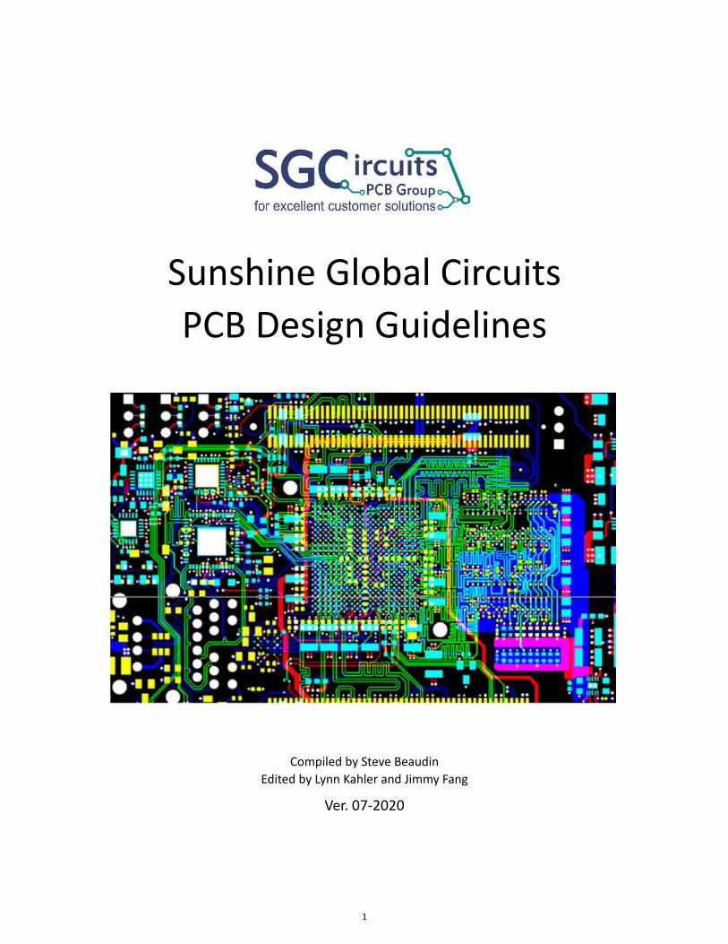
Sunshine Global Circuits
PCB Design Guidelines
Compiled by Steve Beaudin
Edited by Lynn Kahler and Jimmy Fang
Ver. 07‐2020

2
PCB Design Guidelines
Table of Contents
1. Introduction .................................................................................................................................................. 3
2. Incoming Data Requirements ....................................................................................................................... 3
3. Recommended Base Materials ..................................................................................................................... 5
4. Engineering Services ..................................................................................................................................... 6
5. PWB Design Geometry ................................................................................................................................. 7
5.1 Outer Layers ........................................................................................................................................ 7
5.2 Inner layer ............................................................................................................................................ 9
5.3 Drilling ............................................................................................................................................... 11
5.4 Solder Mask ....................................................................................................................................... 13
5.5 Via Plug .............................................................................................................................................. 16
5.6 NC Rout .............................................................................................................................................. 17
5.7 V‐Score .............................................................................................................................................. 17
6. Surface Finishes .......................................................................................................................................... 18
7. Electrical Test .............................................................................................................................................. 18
8. Controlled Impedance ................................................................................................................................ 19
9. Array Panel Guidelines ................................................................................................................................ 21
10. Production Panel and Preferred Sizes ...................................................................................................... 22
11. Contacts .................................................................................................................................................... 23
3
1. Introduction
This document is intended to help the board designer to better understand the process capabilities
and offerings of Sunshine for rigid printed circuit boards. We strongly believe early design
involvement is mutually beneficial and will help improve manufacturability, reduce cycle time, and
lower overall cost. By following these guidelines, the PCB designer will be able to avoid potential
issues and unnecessary delays during the DFM/EQ (engineering question) phase.
We appreciate you taking the time to read and apply this document. As always, please feel free to
contact Sunshine Field Application Engineering or Sales Rep if any questions.
2. Incoming Data Requirements
Below are the preferred data formats and required documentation when issuing orders to Sunshine.
2.1 Data and Documentation Formats
Accepted Image Data Formats
Data formats Gerber RS274‐X
ODB++ (Valor Backup)
Gerber 274‐D – Must include aperture table
IPC‐2581 Rev B
Data Type ASCII
Units Imperial or Metric
Aperture Information
Formats Columnated ASCII
Legible Document
Units Imperial or Metric
NC Drill Data
Formats Excellon II
Plot Data Format
Data Type ASCII
Units Imperial or Metric

4
Fabrication Drawings
Formats Autocad DWG or DXF.*, .dwg,*, .dxf
Portable Data Format: *.pdf
Raster File: *.mil, *.tif, *.gif
Readme Document and/or Special Instructions
Formats ASCII Text File
Embedded within Aperture Information
Legible Document
Net List Data
Formats IPC‐D‐356A
Units Imperial or Metric
2.2 Data Package
Compression Methods
Compression Utility UNIX or DOS/MS Windows
PKWARE Win Zip, PKZip, PKArc UNIX
Unix Compress UNIX
Tar Compress .Tgz DOS
UNIX Pack UNIX
Data Encryption
Encryption Utility Operating System
VLA‐CRYPT PGP MS Windows
UUENCODE Cross Platform
Electronic Data Exchange
FTP (Anonymous or Secured Account)
E‐Mail Attachment
File Share – Secure File Transfer – Contact Sunshine Sales
5
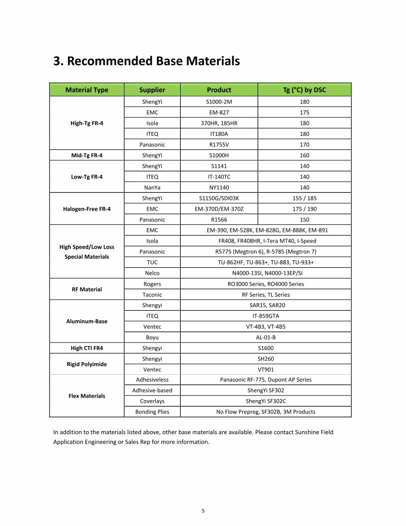
3. Recommended Base Materials
Material Type Supplier Product Tg (°C) by DSC
High‐Tg FR‐4
ShengYi S1000‐2M 180
EMC EM‐827 175
Isola 370HR, 185HR 180
ITEQ IT180A 180
Panasonic R1755V 170
Mid‐Tg FR‐4 ShengYi S1000H 160
Low‐Tg FR‐4
ShengYi S1141 140
ITEQ IT‐140TC 140
NanYa NY1140 140
Halogen‐Free FR‐4
ShengYi S1150G/SDI03K 155 / 185
EMC EM‐370D/EM‐370Z 175 / 190
Panasonic R1566 150
High Speed/Low Loss
Special Materials
EMC EM‐390, EM‐528K, EM‐828G, EM‐888K, EM‐891
Isola FR408, FR408HR, I‐Tera MT40, I‐Speed
Panasonic R5775 (Megtron 6), R‐5785 (Megtron 7)
TUC TU‐862HF, TU‐863+, TU‐883, TU‐933+
Nelco N4000‐13SI, N4000‐13EP/SI
RF Material Rogers RO3000 Series, RO4000 Series
Taconic RF Series, TL Series
Aluminum‐Base
Shengyi SAR15, SAR20
ITEQ IT‐859GTA
Ventec VT‐4B3, VT‐4B5
Boyu AL‐01‐B
High CTI FR4 Shengyi S1600
Rigid Polyimide Shengyi SH260
Ventec VT901
Flex Materials
Adhesiveless Panasonic RF‐775, Dupont AP Series
Adhesive‐based ShengYi SF302
Coverlays ShengYi SF302C
Bonding Plies No Flow Prepreg, SF302B, 3M Products
In addition to the materials listed above, other base materials are available. Please contact Sunshine Field
Application Engineering or Sales Rep for more information.
6
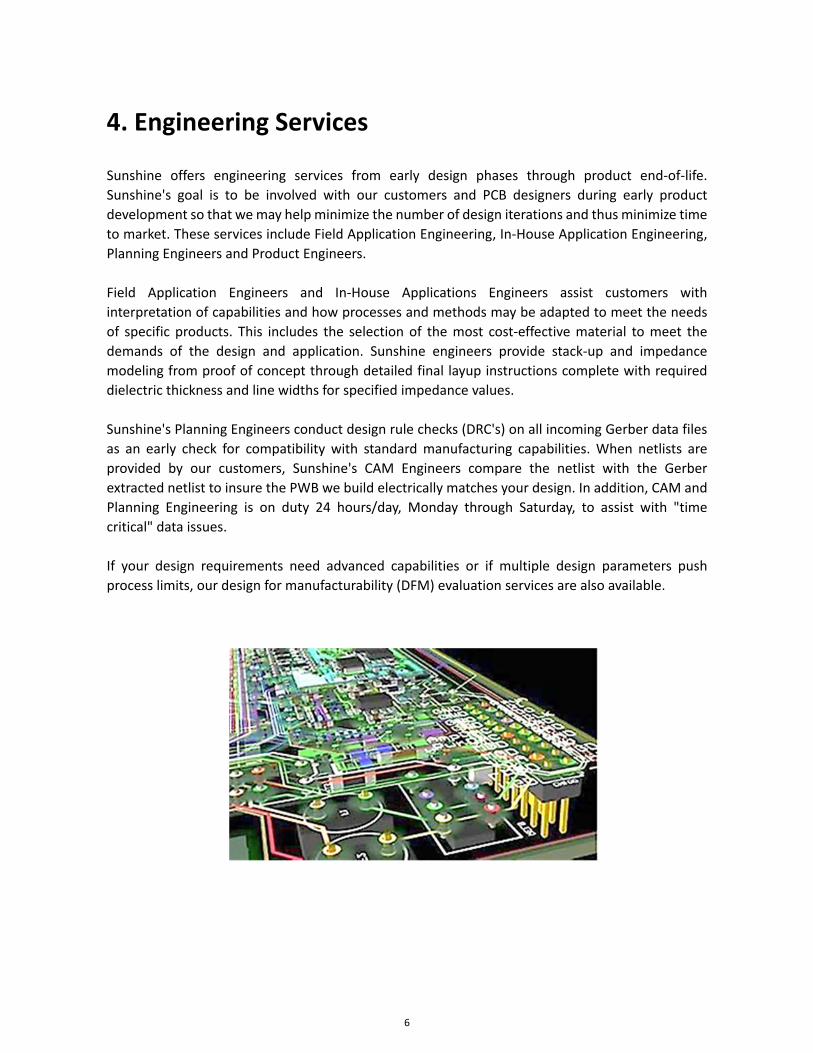
4. Engineering Services
Sunshine offers engineering services from early design phases through product end‐of‐life.
Sunshine's goal is to be involved with our customers and PCB designers during early product
development so that we may help minimize the number of design iterations and thus minimize time
to market. These services include Field Application Engineering, In‐House Application Engineering,
Planning Engineers and Product Engineers.
Field Application Engineers and In‐House Applications Engineers assist customers with
interpretation of capabilities and how processes and methods may be adapted to meet the needs
of specific products. This includes the selection of the most cost‐effective material to meet the
demands of the design and application. Sunshine engineers provide stack‐up and impedance
modeling from proof of concept through detailed final layup instructions complete with required
dielectric thickness and line widths for specified impedance values.
Sunshine's Planning Engineers conduct design rule checks (DRC's) on all incoming Gerber data files
as an early check for compatibility with standard manufacturing capabilities. When netlists are
provided by our customers, Sunshine's CAM Engineers compare the netlist with the Gerber
extracted netlist to insure the PWB we build electrically matches your design. In addition, CAM and
Planning Engineering is on duty 24 hours/day, Monday through Saturday, to assist with "time
critical" data issues.
If your design requirements need advanced capabilities or if multiple design parameters push
process limits, our design for manufacturability (DFM) evaluation services are also available.

7
5. PWB Design Geometry
The following guidelines are provided with “Standard” and “Advanced” options. Items in the
Standard column are current capabilities and can move easily into volume production. Items in the
Advanced column are within our capability but may require additional engineering oversight and
may impact production capacity or cycle time. We are constantly striving to improve our
manufacturing capabilities. If you have questions regarding these guidelines, please reach out to
our Application Engineers or Sales Rep and we will collaborate with you to develop a solution.
All dimensions are in inches unless otherwise noted.
5.1 Outer Layer
Line Width and Spacing (based on H oz starting copper foil)
Item Parameter Standard Advanced
L Minimum Line Width 0.003" 0.0025"
S1 Minimum Space (line to line) 0.0035" 0.0022"
Sp Minimum Space (isolated line array) 0.0035" 0.0025"
h Height of Line 0.0018‐0.0022" 0.0018‐0.0022"
Outer Layer Line Width and Spacing (based on base copper thickness)
Base Copper Minimum Requirement at Design Standard Advanced
0.33oz Line Width/Spacing 0.003”/0.0035” 0.0025”/0.0025”
0.5oz Line Width/Spacing 0.0035”/0.004” 0.0035”/0.0035”
1.0oz Line Width/Spacing 0.004”/0.0045” 0.0035”/0.004”
2.0oz Line Width/Spacing 0.007”/0.007” 0.0065”/0.0065”
3.0oz Line Width/Spacing 0.009”/0.009” 0.0085”/0.0085”
4.0oz Line Width/Spacing 0.011”/0.011” 0.0105”/0.0105”
5.0oz Line Width/Spacing 0.012”/0.012” 0.0115”/0.0115”
8
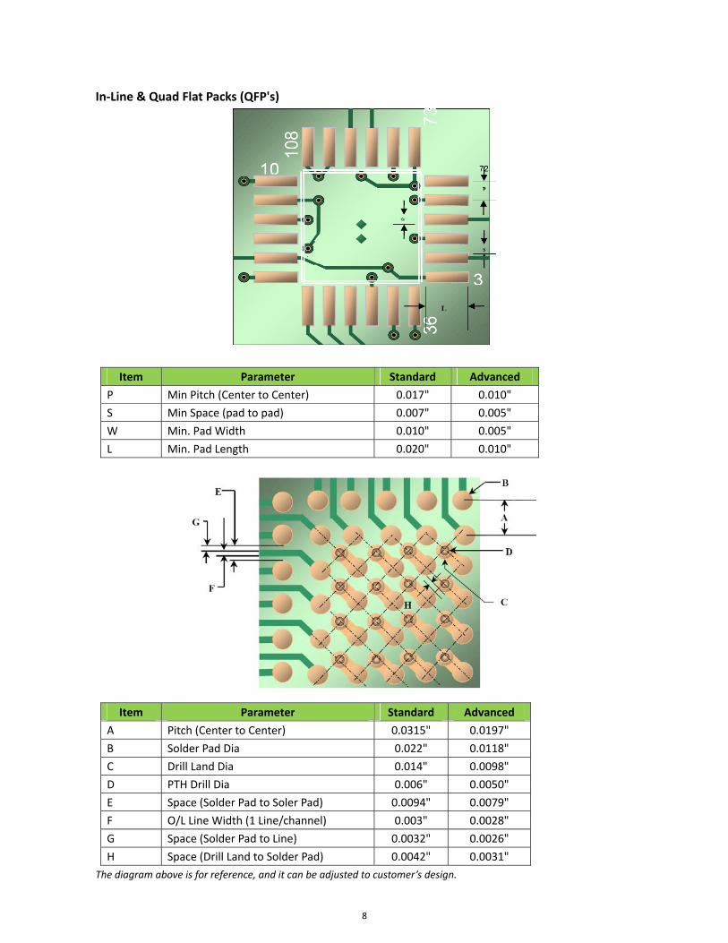
In‐Line & Quad Flat Packs (QFP's)
Item Parameter Standard Advanced
P Min Pitch (Center to Center) 0.017" 0.010"
S Min Space (pad to pad) 0.007" 0.005"
W Min. Pad Width 0.010" 0.005"
L Min. Pad Length 0.020" 0.010"
Item Parameter Standard Advanced
A Pitch (Center to Center) 0.0315" 0.0197"
B Solder Pad Dia 0.022" 0.0118"
C Drill Land Dia 0.014" 0.0098"
D PTH Drill Dia 0.006" 0.0050"
E Space (Solder Pad to Soler Pad) 0.0094" 0.0079"
F O/L Line Width (1 Line/channel) 0.003" 0.0028"
G Space (Solder Pad to Line) 0.0032" 0.0026"
H Space (Drill Land to Solder Pad) 0.0042" 0.0031"
The diagram above is for reference, and it can be adjusted to customer’s design.

9
5.2 Inner Layer
Line Width and Space (based on H oz. copper foil)
Item Parameter Standard Advanced
L Minimum Line Width 0.003" 0.0025"
Sl Minimum Space (line to line) 0.003" 0.003"
Sp Minimum Space (line to via land) 0.005" 0.004"
h Height of Line 0.0006" 0.0006"
Inner Layer Line Width and Spacing (based on copper foil thickness)
Copper Foil Minimum Requirement at Design Standard Advanced
1.0oz Line Width/Spacing 0.0035”/0.0035” 0.003”/0.0035”
2.0oz Line Width/Spacing 0.006”/0.006” 0.0055”/0.0055”
3.0oz Line Width/Spacing 0.008”/0.008” 0.0075”/0.0075”
4.0oz Line Width/Spacing 0.010”/0.010” 0.095”/0.095”
5.0oz Line Width/Spacing 0.012”/0.012” 0.0115”/0.0115”
6.0oz Line Width/Spacing 0.013”/0.013” 0.0125”/0.0125”
Plated Drill to Copper
Item Parameter Standard Advanced
X Drill PTH to Copper Feature 0.01" 0.008"

10
Item Parameter Standard Advanced
C Drilled PTH to Plane 0.010" 0.008"
Item Parameter Standard Advanced
I I/L Land Diameter 0.0167" 0.0118"
J I/L Space (Land to Land) 0.0148" 0.0079"
N I/L Line Width (1 lines/channel) 0.0049" 0.0026"
O I/L Space (Pad to Line) 0.0049" 0.0025"
The diagram above is for reference, and it can be adjusted to customer's design.
Item Parameter Standard
P Plane Clearance (anti‐pad) 0.004"
11
5.3 Drilling
Mechanical Drill
Item Parameter Standard Advanced
D Min. Drilled Hole Diameter 0.01" 0.006"
F Min. Finished Hole Diameter 0.008" 0.004"
Ao Min. Outer Layer Annular Ring 0.005" 0.004"
O/L Land=Drill +2(Ao) 0.020" 0.016"
Ai Min. Inner Layer Annular Ring 0.005" 0.004"
I/L Land=Drill+2(Ai) 0.02" 0.016"
C Clearance (Drill to Plane 0.010" 0.008"
Min. Antipad=Dill+2C 0.034" 0.026"
AR* Max. Aspect Ratio=T/D 8:1 12:1
Mechanical Blind Vias (Controlled Depth) and Buried Vias
Item Parameter Standard Advanced
T Board Thickness (min/max) 0.020/0.200" 0.020/0.250"
D Min. Drilled Hole Diameter 0.01" 0.006"
F Min. Finished Hole Diameter 0.008" 0.004"
d Dielectric Thickness 0.008" 0.005"
dm Controlled Depth Margin (min.) 0.005" 0.003"
AR Blind AR=d/D (max) 0.5:1 0.75:1
Ab Min. Blind/Buried Annular Ring 0.005" 0.004"
Lb Min. Blind/Buried Land 0.02" 0.014"
12
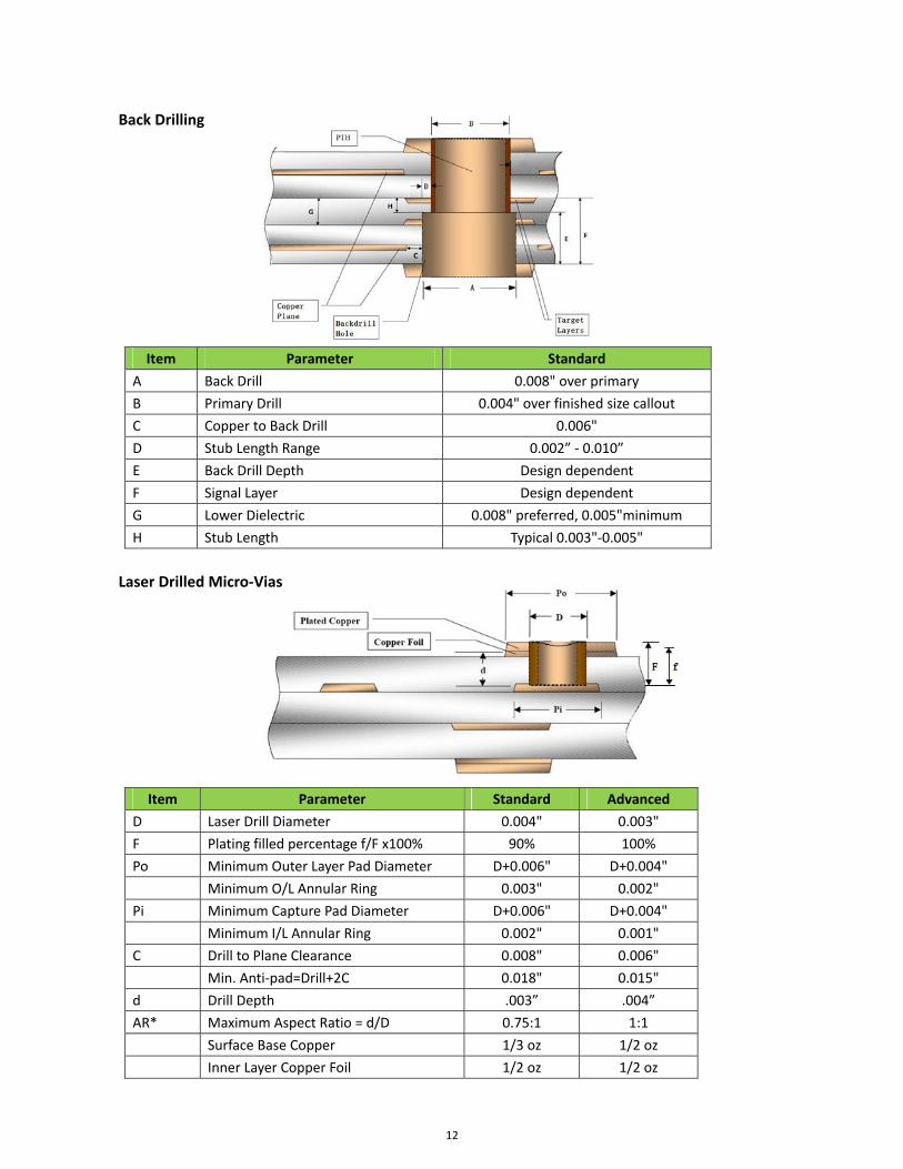
Back Drilling
Item Parameter Standard
A Back Drill 0.008" over primary
B Primary Drill 0.004" over finished size callout
C Copper to Back Drill 0.006"
D Stub Length Range 0.002” ‐ 0.010”
E Back Drill Depth Design dependent
F Signal Layer Design dependent
G Lower Dielectric 0.008" preferred, 0.005"minimum
H Stub Length Typical 0.003"‐0.005"
Laser Drilled Micro‐Vias
Item Parameter Standard Advanced
D Laser Drill Diameter 0.004" 0.003"
F Plating filled percentage f/F x100% 90% 100%
Po Minimum Outer Layer Pad Diameter D+0.006" D+0.004"
Minimum O/L Annular Ring 0.003" 0.002"
Pi Minimum Capture Pad Diameter D+0.006" D+0.004"
Minimum I/L Annular Ring 0.002" 0.001"
C Drill to Plane Clearance 0.008" 0.006"
Min. Anti‐pad=Drill+2C 0.018" 0.015"
d Drill Depth .003” .004”
AR* Maximum Aspect Ratio = d/D 0.75:1 1:1
Surface Base Copper 1/3 oz 1/2 oz
Inner Layer Copper Foil 1/2 oz 1/2 oz
13
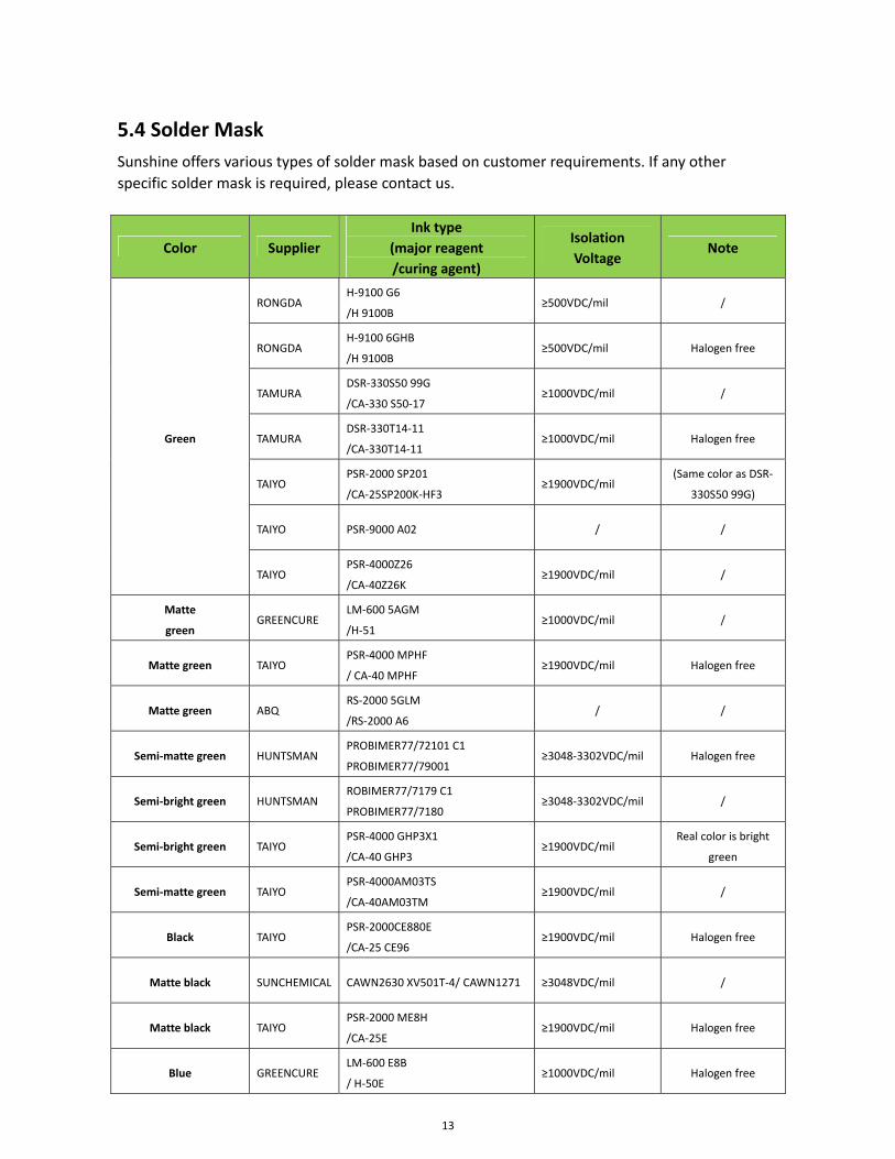
5.4 Solder Mask
Sunshine offers various types of solder mask based on customer requirements. If any other
specific solder mask is required, please contact us.
Color Supplier
Ink type
(major reagent
/curing agent)
Isolation
Voltage Note
Green
RONGDA H‐9100 G6
/H 9100B ≥500VDC/mil /
RONGDA H‐9100 6GHB
/H 9100B ≥500VDC/mil Halogen free
TAMURA DSR‐330S50 99G
/CA‐330 S50‐17 ≥1000VDC/mil /
TAMURA DSR‐330T14‐11
/CA‐330T14‐11 ≥1000VDC/mil Halogen free
TAIYO PSR‐2000 SP201
/CA‐25SP200K‐HF3 ≥1900VDC/mil
(Same color as DSR‐
330S50 99G)
TAIYO PSR‐9000 A02 / /
TAIYO PSR‐4000Z26
/CA‐40Z26K ≥1900VDC/mil /
Matte
green GREENCURE
LM‐600 5AGM
/H‐51 ≥1000VDC/mil /
Matte green TAIYO PSR‐4000 MPHF
/ CA‐40 MPHF ≥1900VDC/mil Halogen free
Matte green ABQ RS‐2000 5GLM
/RS‐2000 A6 / /
Semi‐matte green HUNTSMAN PROBIMER77/72101 C1
PROBIMER77/79001 ≥3048‐3302VDC/mil Halogen free
Semi‐bright green HUNTSMAN ROBIMER77/7179 C1
PROBIMER77/7180 ≥3048‐3302VDC/mil /
Semi‐bright green TAIYO PSR‐4000 GHP3X1
/CA‐40 GHP3 ≥1900VDC/mil
Real color is bright
green
Semi‐matte green TAIYO PSR‐4000AM03TS
/CA‐40AM03TM ≥1900VDC/mil /
Black TAIYO PSR‐2000CE880E
/CA‐25 CE96 ≥1900VDC/mil Halogen free
Matte black SUNCHEMICAL CAWN2630 XV501T‐4/ CAWN1271 ≥3048VDC/mil /
Matte black TAIYO PSR‐2000 ME8H
/CA‐25E ≥1900VDC/mil Halogen free
Blue GREENCURE LM‐600 E8B
/ H‐50E ≥1000VDC/mil Halogen free
14
Color Supplier
Ink type
(major reagent/curing
reagent)
Isolated test
Voltage Note
Matte blue GREENCURE LM‐600 E8BM
/H‐50E ≥1000VDC/mil Halogen free
Matte red GREENCURE LM‐600 8RM
/LM‐600‐B H‐50E ≥1000VDC/mil /
Yellow RONGDA H‐8100 8Y2
/ H‐9100B HD2 ≥500VDC/mil /
Yellow TAIYO PSR‐9000 FLX501OR / /
Purple GREENCURE LM‐600 8PA
/LM‐600‐B H‐50E ≥1000VDC/mil /
White HUNTSMAN PROBIMER77/73100C1
PROBIMER77/79002 ≥3048‐3302VDC/mil Halogen free
White GREENCURE LM‐600 2W87C
/LM‐600‐B H‐W2 ≥1000VDC/mil Halogen free
White TAIYO
PSR‐4000 LEW3
/ CA‐40 LEW3
≥1900VDC/mil /
White TAIYO PSR‐4000WT02
/ CA‐40WT02 ≥1900VDC/mil Halogen free
White LANBANG LB‐1900 W‐8A / Halogen free
Matte white GREENCURE LM‐600 2KWM
/H‐53 ≥1000VDC/mil Halogen free
Matte white ABQ RS‐2000 WDM‐1
/RS‐2000 A6 / /
Green TAIYO PSR‐4000 PF9NB
/CA‐40PF9 ≥1900VDC/mil
Ink for solder mask
plugging
Transparent ANRANSENG APS800 T01
/APS‐800H ≥1000VDC/mil /
Legend Ink
Color Supplier Ink type Range of Application (internal regulation) Note
Green ANRANSHENG AT‐600G03 Plug hole and thermal cure after surface
treatment Thermal cure
White TAIYO IJR‐4000 MW300 White,ink for legend printing /
White TAIYO S‐200W N30/HD‐3 All white word board made by silkscreen /
White TAIYO S‐411W/HD‐C All white word halogen free board made by
silkscreen Halogen free
Yellow TAIYO S‐200Y ND/HD‐3 All yellow word board made by silkscreen /
Black TAIYO S‐200E/HD‐3 All black word board made by silkscreen /
15
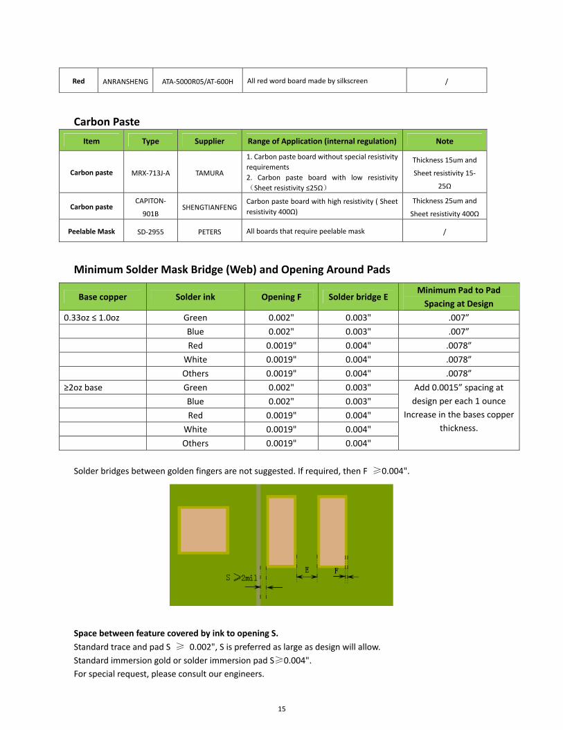
Red ANRANSHENG ATA‐5000R05/AT‐600H All red word board made by silkscreen /
Carbon Paste
Item Type Supplier Range of Application (internal regulation) Note
Carbon paste MRX‐713J‐A TAMURA
1. Carbon paste board without special resistivity
requirements
2. Carbon paste board with low resistivity
(Sheet resistivity ≤25Ω)
Thickness 15um and
Sheet resistivity 15‐
25Ω
Carbon paste CAPITON‐
901B SHENGTIANFENG
Carbon paste board with high resistivity ( Sheet
resistivity 400Ω)
Thickness 25um and
Sheet resistivity 400Ω
Peelable Mask SD‐2955 PETERS All boards that require peelable mask /
Minimum Solder Mask Bridge (Web) and Opening Around Pads
Base copper Solder ink Opening F Solder bridge E Minimum Pad to Pad
Spacing at Design
0.33oz ≤ 1.0oz Green 0.002" 0.003" .007”
Blue 0.002" 0.003" .007”
Red 0.0019" 0.004" .0078”
White 0.0019" 0.004" .0078”
Others 0.0019" 0.004" .0078”
≥2oz base Green 0.002" 0.003" Add 0.0015” spacing at
design per each 1 ounce
Increase in the bases copper
thickness.
Blue 0.002" 0.003"
Red 0.0019" 0.004"
White 0.0019" 0.004"
Others 0.0019" 0.004"
Solder bridges between golden fingers are not suggested. If required, then F ≥0.004".
Space between feature covered by ink to opening S.
Standard trace and pad S ≥ 0.002", S is preferred as large as design will allow.
Standard immersion gold or solder immersion pad S≥0.004".
For special request, please consult our engineers.

16
Solder Mask Thickness
Base copper weight Solid Copper A Corner B Trace C Base material D
Hoz 15‐40um 5‐35um 10‐35um 15‐60um
1oz 15‐40um 5‐35um 10‐35um 15‐80um
1.5‐2oz 15‐40um 5‐35um 10‐35um 15‐100um
1.5‐2oz (thick) 30‐70um 10‐50um 15‐60um 30‐130um
3oz 30‐70um 10‐50um 15‐60um 30‐165um
≥4oz 30‐70um 10‐50um 15‐60um 30‐um
5.5 Via Plug
Solder Mask Ink Plugging
Board thickness: 0.024” ≤ 0.110”
For double sided plugging, hole diameter ≤0.018”.
For one sided plugging, if hole diameter is ≥0.45 and ≤ 0.6mm, plugged but not filled design is recommended.
Vacuum Resin Plugging (VIPPO or Non‐conductive fill and plate over)
Minimum hole/blind hole diameter 0.1mm,
Maximum hole diameter equal to board thickness when board thickness ≤4mm.
Board aspect ratio ≤25:1.
Double side h/H x100% ≥ 98%, one side D2=0.001".
17
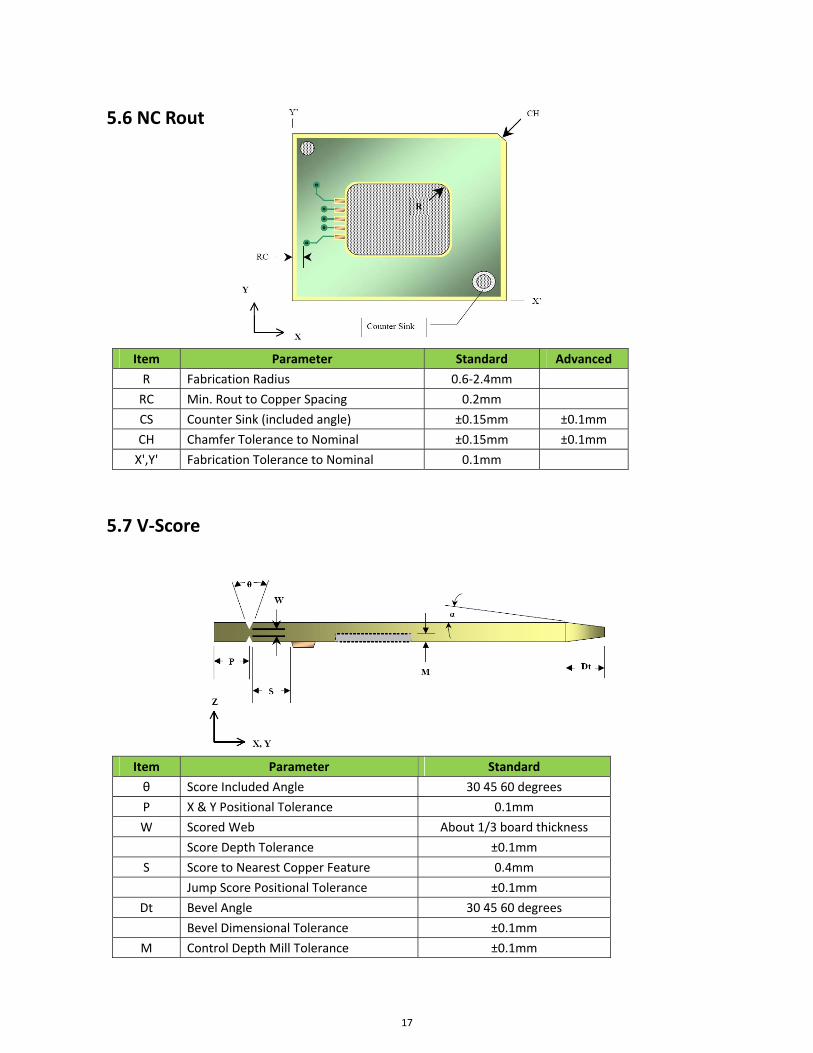
5.6 NC Rout
Item Parameter Standard Advanced
R Fabrication Radius 0.6‐2.4mm
RC Min. Rout to Copper Spacing 0.2mm
CS Counter Sink (included angle) ±0.15mm ±0.1mm
CH Chamfer Tolerance to Nominal ±0.15mm ±0.1mm
X',Y' Fabrication Tolerance to Nominal 0.1mm
5.7 V‐Score
Item Parameter Standard
θ Score Included Angle 30 45 60 degrees
P X & Y Positional Tolerance 0.1mm
W Scored Web About 1/3 board thickness
Score Depth Tolerance ±0.1mm
S Score to Nearest Copper Feature 0.4mm
Jump Score Positional Tolerance ±0.1mm
Dt Bevel Angle 30 45 60 degrees
Bevel Dimensional Tolerance ±0.1mm
M Control Depth Mill Tolerance ±0.1mm

18
6. Surface Finishes
Individual Types Suggested Parameters
Hot Air Solder Level(HASL) 1‐40um
Electrolytic Nickel/Gold Ni:100 µ"minimum Flash Au:3‐10 µ"
Hard Au: 3‐50 µ"
Soft Au: 3‐30 µ"
Electroless Ni/Immersion Au Ni:118 – 236 µ" Au: 2‐6 µ" Per IPC‐4552
Immersion Tin Sn:8‐12 µ"
Immersion Silver Ag: 8‐12 µ" – Per IPC‐4553
OSP 0.2‐0.5 µm
Combination Finishes Suggested Parameters
HASL & Selective Electrolytic Ni/Au (HASL for
solder pads with Ni/Au on contact pads)
Ni:118 – 236 µ" Hard Au 35‐50 µ"
Selective Electrolytic Ni/Au
(Thin Au for soldering, thick for wire bonding)
Ni:118 – 236 µ" Soft Au: 3‐8 µ" & 35‐50 µ"
Selective Electrolytic Ni/Au
(Thin Au for soldering, thick for contact pads)
Ni:118 – 236 µ" Hard Au: 3‐8 µ" & 35‐50 µ"
Selective Electrolytic Ni/Au and OSP Wire Bond
or Contact Pads Solder Pads
Ni:118 – 236 µ"
OSP: 0.2‐0.5 µm
Soft or Hard Au 35‐50µ"
7. Electrical Test
Netlist Testing
Sunshine offers a wide range of electrical test equipment and capabilities. Most bare board testing
is done on universal grid testers with test fixtures built in‐house. For small lots or extremely fine
pitch configurations, flying probe testers are used.
HIPOT Testing
HIPOT testing is conducted at inner layer process as wells on finished raw PCB's to insure isolation
between all power / ground planes. Testing may be conducted with respect to current leakage or
mΩ resistance between biased layers. With the trend toward decreasing thickness of dielectric
layers it is necessary to re‐think the traditional 500V HIPOT test. Boards designed with 0.002" (or
less) dielectrics and nominal spacing between drilled vias and planes <0.01" may not be able to
withstand a 500V bias and meet required current leakage or mΩ resistance standards. Consideration

19
needs to be given to the actual working voltage of the board under test and the maximum expected
transient voltage when deciding how best to design a HIPOT rest for a given PCB.
8. Controlled Impedance
Controlled impedance lines may be designed in many different configurations. The most common
are microstrip and stripline. Variations of these basic forms include microstrip with and without
solder mask, embedded microstrip, differential microstrip, and guarded microstrip. Stripline,
broadside differential stripline, and guarded variations.
Specify on the master drawing which signal layers are to be controlled impedance layers, the line
width in the Gerber data that represents the controlled impedance lines, and the desired value and
tolerance.
Example: 50Ω impedance, +/‐10%, on 0.004" lines on all internal signal layers and on 0.007" lines
on outer layers.
If more than on impedance value is required on a given layer and/or there are various controlled
impedance structures within the same PCB, it is beneficial to create an Impedance Table on the
master drawing that indicates layer, trace width & impedance value, reference planes, impedance
structure type, and line width. If 0.005" lines are to be 50Ω single‐ended and other 0.005" lines on
the same layer are to be 100Ω differential pairs it is best to rout the differential pairs at a slightly
different width (i.e. 0.0051”) so CAM operators can make minor adjustments to the final etched line
width to meet you requirements.
Parameter Standard Advanced
Impedance Tolerance ≥ 50 ohms ±10% ±8%
Impedance Tolerance ≤ 50 ohm ±5 ohm ±3.5ohms

20
Test hole diameter: 1.0‐1.2MM, pitch to pitch distance: 0.1".
Example Table:
Controlled Impedance Requirements
Layer Lines Pitch Ref. Layer Impedance(Ω) Tolerance(%)
Top 0.007" N/A 2 50 SE 10
3 0.005" N/A 2&4 50 SE 10
3 0.0051" 0.015" 2&4 100 Diff 10
6 0.005" N/A 5&7 50 SE 10
6 0.0051" 0.015" 5&7 100 Diff 10
Bottom 0.007" N/A 7 50 SE 10
It is desirable to add a statement to the effect that final impedance values take precedence over line
widths. Minor adjustment in dielectric layers and line widths are usually required to come as close
as possible to your target values.
The variables of controlled impedance structures include the following:
1. Thickness of the copper signal trace
2. Width of the copper signal trace (Top/Bottom)
3. Thickness of the dielectric material between the trace and the reference plane
4. Pitch of differential pairs
5. Horizontal distance to ground guards

21
Sunshine uses time domain reflectometry (TDR) for testing impedance on PCB's. Testing validation
is conducted with a coupon representing the design’s structure from the production panel. The
coupon’s design incorporates the same geometry of the PCB with respect to dielectric thickness,
copper weights, line widths, configuration etc. It is important to specify your impedance
requirements on the master drawing. TDR reports are available with all controlled impedance orders.
9. Array Panel Guidelines
Many customers require their boards to be panelized with suitable rails so the product can be run
down an automated assembly line. It is best that an assembly array drawing or guidelines are
supplied at the time of quoting. Please check with your contract manufacturer (CM) regarding their
array preferences. However, we will cover a few basics on array panels.
There is basic information required to design the assembly array:
1. Depanelization method:
a. V‐score
b. Tab with break holes (Rout and Retain)
c. Solid tabs with V‐score
d. Solid tabs – no break holes (To be routed out by the CM after assembly)
2. Minimum or maximum array panel size (this can vary by CM or equipment):
a. Typical minimum is 5.000” x 4.250” including the rails.
b. Typical maximums:
i. Board thickness ≤ 0.031” – ~11.00” x 9.00” including the rails.
ii. Board thickness > 0.031” – ~19.00” x 14.00” including the rails.
3. Array requirements.
a. Fiducials:
i. Minimum pad size – 1.6mm is suggested minimum size
ii. Minimum number of fiducials per side – We default to 3 per side
iii. Minimum distance from board or panel edge – We default to center of rail
b. Tooling holes:
i. Minimum size – our typical minimum is 1mm to 3.2mm based on the rail
size.
ii. We prefer a minimum of 3 tooling holes towards the corners of the array
panel.

22
c. Constraints and other notes:
i. Overhanging components must be considered
ii. Keep out areas for connectors or other areas that require special attention
should be noted
iii. Minimum of 2mm spacing is required between boards for double V‐cutting
iv. Board orientation ‐ can boards be rotated 180° for better material usage?
v. If board is thin or long between assembly rails, warpage may be an issue.
10. Production Panel Information
One of the largest cost factors in offshore manufacturing is the base material cost. Here is some
information to help optimize your design for best material use practices.
Sunshine purchases laminates in full sheets from the material supplier and cuts the sheets into
working panels for fabrication. Sheet sizes include 43”x49, 41”x49”, and 37”x49”. Below is a list of
our preferred working panel sizes for best material usage.
Other sizes are available; please contact us for more information.
Shenzhen Factory Preferred Sizes Jiujiang Factory Preferred Sizes
24x21 inch (610 x 533 mm) 24x21 inch (610 x 533 mm)
24x20 inch (610 x 508 mm) 24x20 inch (610 x 508 mm)
24x18 inch (610 x 457 mm) 24x18 inch (610 x 457 mm)
24x14 inch (610 x 356 mm) 24x14 inch (610 x 356 mm)
16x21 inch (406 x 533 mm) 24x13 inch (610 x 330 mm)
16x20 inch (406 x 508 mm) 24x12 inch (610 x 305 mm)
16x18 inch (406 x 457 mm) 16x21 inch (406 x 533 mm)
16x20 inch (406 x 508 mm)
16x18 inch (406 x 457 mm)
Allow minimum 0.6” border for tooling and coupons and minimum .08” (2mm) between arrays.
23
11. Contacts
All information in this document is provided as a guideline to assist Sunshine customers in
developing PCB designs that meet the DFM requirements for manufacturing and to help minimize
any delays during the EQ and production process. If any suggestions or questions regarding this
document, please contact us as shown below.
Sunshine Global Circuits
USA Engineering Support
3400 Silverstone Drive, Suite 139, Plano, Texas, USA 75023
Office 982‐867‐8886
Steve Beaudin, Sr. Application Engineer
Mobile 469‐236‐0513
Lynn Kahler, Regional Sales Manager
Mobile 214‐412‐4286