subject : ec1209 electron devices and circuits · pdf filesubject : ec1209 – electron...
TRANSCRIPT
DEPARTMENT : ELECTRICAL AND ELECTRONICS ENGINEERING
SUBJECT : EC1209 – ELECTRON DEVICES AND CIRCUITS
YEAR : II
SEMESTER : III


EC1209 – ELECTRON DEVICES AND CIRCUITS
UNIT I SEMICONDUCTOR DIODE AND BJT
PN Junction – Current components in a PN diode – Junction capacitance – Junction diode
switching time – Zener diode – Varactor diode – Tunnel diode – Schottky diode –
Transistor Structure – Basic Transistor operation – Transistor characteristics and
parameters – Transistor as a switch and amplifier – Transistor bias circuit – Voltage
divider bias circuits – Base bias circuits – Emitter bias circuits – Collector feedback bias
circuits – DC load line – AC load line – Bias stabilization – Thermal runaway and
thermal stability.
UNIT II FET, UJT and SCR
JFET characteristics and parameters – JFET biasing – Self bias – Voltage divider bias –
Q point – Stability over temperature – MOSFET – D-MOSFET and E-MOSFET –
MOSFET characteristics and parameters – MOSFET biasing – Zero bias – Voltage
divider bias – Drain feedback bias – Characteristics and applications of UJT, SCR,
DIAC, TRIAC.
UNIT III AMPLIFIERS
CE, CC and CB amplifiers – Small-signal low frequency transistor amplifier circuits –
h-parameter representation of a transistor – Analysis of single stage transistor amplifier
circuits – Voltage gain – Current gain – Input impedance and output impedance –
Frequency response – RC coupled amplifier – Classification of Power amplifiers – Class
A, B, AB and C Power amplifiers – Push-Pull and Complementary-Symmetry amplifiers
– Design of power output, efficiency and cross-over distortion.
UNIT IV FEEDBACK AMPLIFIERS AND OSCILLATORS
Advantages of negative feedback – Voltage/current, series/shunt feedback – Positive
feedback – Conditions for oscillation – Phase shift – Wein Bridge – Hartley – Colpitts
and Crystal oscillators.
UNIT V PULSE CIRCUITS AND POWER SUPPLY

RC wave shaping circuits – Diode clampers and clippers – Multivibrators – Schmitt
triggers – UJT saw-tooth oscillators – Single and poly-phase rectifiers and analysis of
filter circuits – Design of zener and transistor series voltage regulators – Switched mode
power supplies.
Total: 45
TEXT BOOKS
1. Robert T. Paynter, ―Introductory Electronic Devices and Circuits‖, 7th Edition,
Pearson Education, 2006.
2. Millman and Halkias, ―Electronic Devices and Circuits‖, Tata McGraw Hill, 2007.
REFERENCES
1. Mottershead, A., ―Electronic Devices and Circuits an Introduction‖, Prentice Hall of
India, 2003.
2. Boylsted and Nashelsky, ―Electronic Devices and Circuit Theory‖, Prentice Hall of
India, 6th Edition, 1999.
3. Bell, D.A., ―Electronic Devices and Circuits‖, Oxford University Press, 4th Edition,
1999.

UNIT I
SEMICONDUCTOR DIODE AND BJT
PN Junction – Current components in a PN diode – Junction capacitance – Junction diode
switching time – Zener diode – Varactor diode – Tunnel diode – Schottky diode –
Transistor Structure – Basic Transistor operation – Transistor characteristics and
parameters – Transistor as a switch and amplifier – Transistor bias circuit – Voltage
divider bias circuits – Base bias circuits – Emitter bias circuits – Collector feedback bias
circuits – DC load line – AC load line – Bias stabilization – Thermal runaway and
thermal stability.
UNIT I
SEMICONDUCTOR DIODE AND BJT
Semiconductor diodes
A modern semiconductor diode is made of a crystal of semiconductor like
silicon that has impurities added to it to create a region on one side that
contains negative charge carriers (electrons), called n-type semiconductor,
and a region on the other side that contains positive charge carriers (holes),
called p-type semiconductor. The diode's terminals are attached to each of
these regions. The boundary within the crystal between these two regions,
called a PN junction, is where the action of the diode takes place. The crystal
conducts conventional current in a direction from the p-type side (called
the anode) to the n-type side (called the cathode), but not in the opposite
direction.
Another type of semiconductor diode, the Schottky diode, is formed from
the contact between a metal and a semiconductor rather than by a p-n
junction.
Current–voltage characteristic
A semiconductor diode‘s behavior in a circuit is given by its current–voltage
characteristic, or I–V graph (see graph below). The shape of the curve is
determined by the transport of charge carriers through the so-
called depletion layer or depletion region that exists at the p-n
junction between differing semiconductors. When a p-n junction is first
created, conduction band (mobile) electrons from the N-doped region diffuse
into the P-doped region where there is a large population of holes (vacant
places for electrons) with which the electrons ―recombine‖. When a mobile
electron recombines with a hole, both hole and electron vanish, leaving
behind an immobile positively charged donor (dopant) on the N-side and
negatively charged acceptor (dopant) on the P-side. The region around the p-
n junction becomes depleted of charge carriers and thus behaves as
an insulator.
However, the width of the depletion region (called the depletion width)
cannot grow without limit. For each electron-hole pair that recombines, a
positively charged dopant ion is left behind in the N-doped region, and a
negatively charged dopant ion is left behind in the P-doped region. As
recombination proceeds more ions are created, an increasing electric field
develops through the depletion zone which acts to slow and then finally stop
recombination. At this point, there is a ―built-in‖ potential across the
depletion zone.
If an external voltage is placed across the diode with the same polarity as the
built-in potential, the depletion zone continues to act as an insulator,
preventing any significant electric current flow (unless electron/hole pairs
are actively being created in the junction by, for instance, light.
see photodiode). This is the reverse bias phenomenon. However, if the
polarity of the external voltage opposes the built-in potential, recombination
can once again proceed, resulting in substantial electric current through the
p-n junction (i.e. substantial numbers of electrons and holes recombine at the
junction). For silicon diodes, the built-in potential is approximately 0.7 V
(0.3 V for Germanium and 0.2 V for Schottky). Thus, if an external current
is passed through the diode, about 0.7 V will be developed across the diode
such that the P-doped region is positive with respect to the N-doped region
and the diode is said to be ―turned on‖ as it has a forward bias.
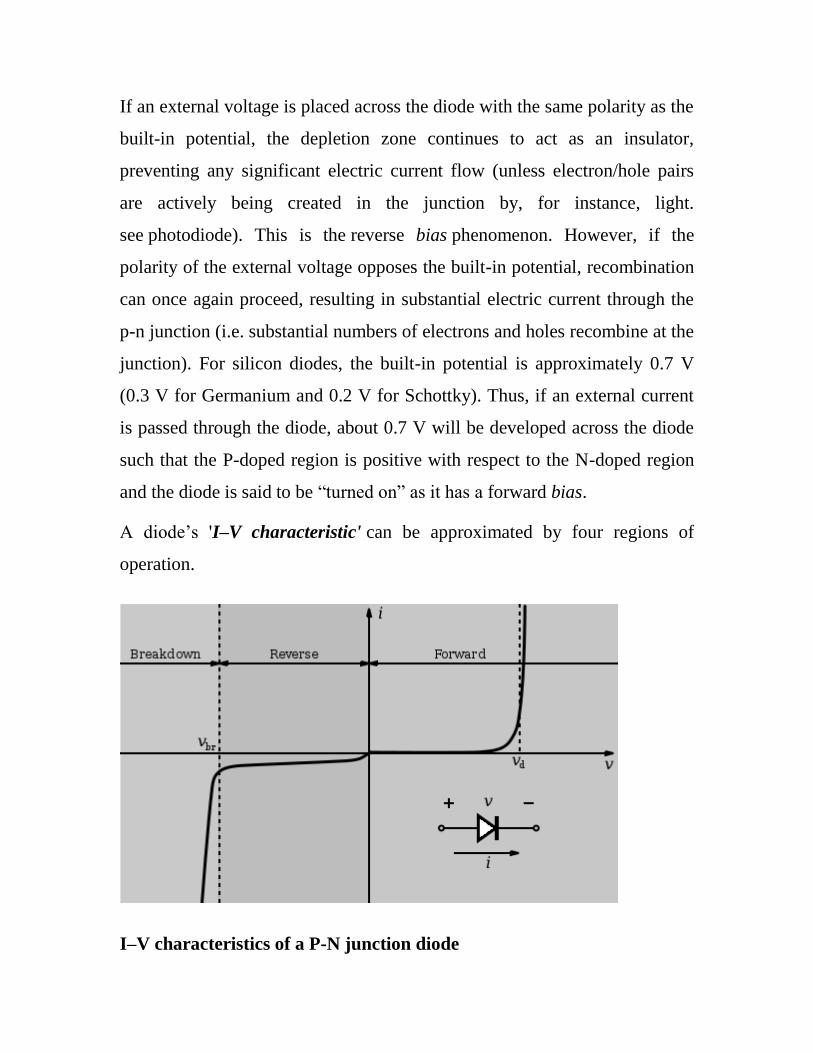
A diode‘s 'I–V characteristic' can be approximated by four regions of
operation.
I–V characteristics of a P-N junction diode

At very large reverse bias, beyond the peak inverse voltage or PIV, a process
called reverse breakdown occurs which causes a large increase in current
(i.e. a large number of electrons and holes are created at, and move away
from the pn junction) that usually damages the device permanently.
The avalanche diode is deliberately designed for use in the avalanche region.
In the zener diode, the concept of PIV is not applicable. A zener diode
contains a heavily doped p-n junction allowing electrons to tunnel from the
valence band of the p-type material to the conduction band of the n-type
material, such that the reverse voltage is ―clamped‖ to a known value (called
the zener voltage), and avalanche does not occur. Both devices, however, do
have a limit to the maximum current and power in the clamped reverse
voltage region. Also, following the end of forward conduction in any diode,
there is reverse current for a short time. The device does not attain its full
blocking capability until the reverse current ceases.
The second region, at reverse biases more positive than the PIV, has only a
very small reverse saturation current. In the reverse bias region for a normal
P-N rectifier diode, the current through the device is very low (in the µA
range). However, this is temperature dependent, and at sufficiently high
temperatures, a substantial amount of reverse current can be observed (mA
or more).
The third region is forward but small bias, where only a small forward
current is conducted.
As the potential difference is increased above an arbitrarily defined ―cut-in
voltage‖ or ―on-voltage‖ or ―diode forward voltage drop (Vd)‖, the diode
current becomes appreciable (the level of current considered ―appreciable‖
and the value of cut-in voltage depends on the application), and the diode

presents a very low resistance. The current–voltage curve is exponential. In a
normal silicon diode at rated currents, the arbitrary ―cut-in‖ voltage is
defined as 0.6 to 0.7 volts. The value is different for other diode types —
Schottky diodes can be rated as low as 0.2 V, Germanium diodes 0.25-0.3
V, and red or blue light-emitting diodes (LEDs) can have values of 1.4 V
and 4.0 V respectively.
At higher currents the forward voltage drop of the diode increases. A drop of
1 V to 1.5 V is typical at full rated current for power diodes.
Shockley diode equation
The Shockley ideal diode equation or the diode law (named
after transistor co-inventor William Bradford Shockley, not to be confused
with tetrode inventor Walter H. Schottky) gives the I–V characteristic of an
ideal diode in either forward or reverse bias (or no bias). The equation is:
where
I is the diode current,
IS is the reverse bias saturation current (or scale current),
VD is the voltage across the diode,
VT is the thermal voltage, and
n is the ideality factor, also known as the quality factor or
sometimes emission coefficient. The ideality factor n varies from 1 to 2

depending on the fabrication process and semiconductor material and in
many cases is assumed to be approximately equal to 1 (thus the notation n is
omitted).
The thermal voltage VT is approximately 25.85 mV at 300 K, a temperature
close to ―room temperature‖ commonly used in device simulation software.
At any temperature it is a known constant defined by:
where k is the Boltzmann constant, T is the absolute temperature of the p-n
junction, and q is the magnitude of charge on an electron (the elementary
charge).
The Shockley ideal diode equation or the diode law is derived with the
assumption that the only processes giving rise to the current in the diode are
drift (due to electrical field), diffusion, and thermal recombination-
generation. It also assumes that the recombination-generation (R-G) current
in the depletion region is insignificant. This means that the Shockley
equation doesn‘t account for the processes involved in reverse breakdown
and photon-assisted R-G. Additionally, it doesn‘t describe the ―leveling off‖
of the I–V curve at high forward bias due to internal resistance.
Under reverse bias voltages (see Figure 5) the exponential in the diode
equation is negligible, and the current is a constant (negative) reverse current
value of −IS. The reverse breakdown region is not modeled by the Shockley
diode equation.
For even rather small forward bias voltages (see Figure 5) the exponential is
very large because the thermal voltage is very small, so the subtracted ‗1‘ in

the diode equation is negligible and the forward diode current is often
approximated as
The use of the diode equation in circuit problems is illustrated in the article
on diode modeling.
Several types of junction diodes
There are several types of junction diodes, which either emphasize a
different physical aspect of a diode often by geometric scaling, doping level,
choosing the right electrodes, are just an application of a diode in a special
circuit, or are really different devices like the Gunn and laser diode and
the MOSFET:
Normal (p-n) diodes, which operate as described above, are usually made of
doped silicon or, more rarely, germanium. Before the development of
modern silicon power rectifier diodes, cuprous oxide and later selenium was
used; its low efficiency gave it a much higher forward voltage drop
(typically 1.4–1.7 V per ―cell‖, with multiple cells stacked to increase the
peak inverse voltage rating in high voltage rectifiers), and required a large
heat sink (often an extension of the diode‘s metal substrate), much larger
than a silicon diode of the same current ratings would require. The vast
majority of all diodes are the p-n diodes found inCMOS integrated circuits,
which include two diodes per pin and many other internal diodes.
Avalanche diodes
Diodes that conduct in the reverse direction when the reverse bias voltage
exceeds the breakdown voltage. These are electrically very similar to Zener
diodes, and are often mistakenly called Zener diodes, but break down by a

different mechanism, the avalanche effect. This occurs when the reverse
electric field across the p-n junction causes a wave of ionization, reminiscent
of an avalanche, leading to a large current. Avalanche diodes are designed to
break down at a well-defined reverse voltage without being destroyed. The
difference between the avalanche diode (which has a reverse breakdown
above about 6.2 V) and the Zener is that the channel length of the former
exceeds the ―mean free path‖ of the electrons, so there are collisions
between them on the way out. The only practical difference is that the two
types have temperature coefficients of opposite polarities.
Constant current diodes
These are actually a JFET with the gate shorted to the source, and function
like a two-terminal current-limiter analog to the Zener diode, which is
limiting voltage. They allow a current through them to rise to a certain value,
and then level off at a specific value. Also called CLDs, constant-current
diodes, diode-connected transistors, or current-regulating diodes.
Esaki or tunnel diodes
These have a region of operation showing negative resistance caused
by quantum tunneling, thus allowing amplification of signals and very
simple bistable circuits. These diodes are also the type most resistant to
nuclear radiation.
Gunn diodes
These are similar to tunnel diodes in that they are made of materials such as
GaAs or InP that exhibit a region of negative differential resistance. With
appropriate biasing, dipole domains form and travel across the diode,
allowing high frequency microwave oscillators to be built.

Light-emitting diodes (LEDs)
In a diode formed from a direct band-gap semiconductor, such as gallium
arsenide, carriers that cross the junction emit photons when they recombine
with the majority carrier on the other side. Depending on the
material, wavelengths (or colors)[11]
from the infrared to the
near ultraviolet may be produced.[12]
The forward potential of these diodes
depends on the wavelength of the emitted photons: 1.2 V corresponds to red,
2.4 V to violet. The first LEDs were red and yellow, and higher-frequency
diodes have been developed over time. All LEDs produce incoherent,
narrow-spectrum light; ―white‖ LEDs are actually combinations of three
LEDs of a different color, or a blue LED with a yellow scintillator coating.
LEDs can also be used as low-efficiency photodiodes in signal applications.
An LED may be paired with a photodiode or phototransistor in the same
package, to form an opto-isolator.
Laser diodes
When an LED-like structure is contained in a resonant cavity formed by
polishing the parallel end faces, a laser can be formed. Laser diodes are
commonly used in optical storage devices and for high speed optical
communication.
Thermal diodes
This term is used both for conventional PN diodes used to monitor
temperature due to their varying forward voltage with temperature, and
for Peltier heat pumps for thermoelectric heating and cooling.. Peltier heat

pumps may be made from semiconductor, though they do not have any
rectifying junctions, they use the differing behaviour of charge carriers in N
and P type semiconductor to move heat.
Photodiodes
All semiconductors are subject to optical charge carrier generation. This is
typically an undesired effect, so most semiconductors are packaged in light
blocking material. Photodiodes are intended to sense light(photodetector), so
they are packaged in materials that allow light to pass, and are usually PIN
(the kind of diode most sensitive to light).[13]
A photodiode can be used
in solar cells, in photometry, or in optical communications. Multiple
photodiodes may be packaged in a single device, either as a linear array or as
a two-dimensional array. These arrays should not be confused with charge-
coupled devices.
Point-contact diodes
These work the same as the junction semiconductor diodes described above,
but their construction is simpler. A block of n-type semiconductor is built,
and a conducting sharp-point contact made with some group-3 metal is
placed in contact with the semiconductor. Some metal migrates into the
semiconductor to make a small region of p-type semiconductor near the
contact. The long-popular 1N34 germanium version is still used in radio
receivers as a detector and occasionally in specialized analog electronics.
PIN diodes

A PIN diode has a central un-doped, or intrinsic, layer, forming a p-
type/intrinsic/n-type structure.[14]
They are used as radio frequency switches
and attenuators. They are also used as large volume ionizing radiation
detectors and as photodetectors. PIN diodes are also used in power
electronics, as their central layer can withstand high voltages. Furthermore,
the PIN structure can be found in many power semiconductor devices, such
as IGBTs, power MOSFETs, and thyristors.
Schottky diodes
Schottky diodes are constructed from a metal to semiconductor contact.
They have a lower forward voltage drop than p-n junction diodes. Their
forward voltage drop at forward currents of about 1 mA is in the range
0.15 V to 0.45 V, which makes them useful in voltage clamping
applications and prevention of transistor saturation. They can also be used as
low loss rectifiers although their reverse leakage current is generally higher
than that of other diodes. Schottky diodes are majority carrier devices and so
do not suffer from minority carrier storage problems that slow down many
other diodes — so they have a faster ―reverse recovery‖ than p-n junction
diodes. They also tend to have much lower junction capacitance than p-n
diodes which provides for high switching speeds and their use in high-speed
circuitry and RF devices such as switched-mode power
varactor diodes

Varactors are operated reverse-biased so no current flows, but since the
thickness of the depletion zone varies with the applied bias voltage, the
capacitance of the diode can be made to vary. Generally, the depletion
region thickness is proportional to the square root of the applied voltage;
andcapacitance is inversely proportional to the depletion region thickness.
Thus, the capacitance is inversely proportional to the square root of applied
voltage.
All diodes exhibit this phenomenon to some degree, but specially made
varactor diodes exploit the effect to boost the capacitance and variability
range achieved - most diode fabrication attempts to achieve the opposite.
In the figure we can see an example of a crossection of a varactor with the
depletion layer formed of a p-n-junction. But the depletion layer can also be
made of a MOS-diode or a Schottky diode. This is very important
in CMOS and MMIC technology.
Zener diodes
Diodes that can be made to conduct backwards. This effect, called Zener
breakdown, occurs at a precisely defined voltage, allowing the diode to be
used as a precision voltage reference. In practical voltage reference circuits
Zener and switching diodes are connected in series and opposite directions
to balance the temperature coefficient to near zero. Some devices labeled as
high-voltage Zener diodes are actually avalanche diodes (see above). Two
(equivalent) Zeners in series and in reverse order, in the same package,
constitute a transient absorber (or Transorb, a registered trademark). The
Zener diode is named for Dr. Clarence Melvin Zener of Carnegie Mellon
University, inventor of the device.
Other uses for semiconductor diodes include sensing temperature, and
computing analog logarithms (see Operational amplifier
applications#Logarithmic).

Zener diode is a type of diode that permits current not only in the forward
direction like a normal diode, but also in the reverse direction if the voltage
is larger than the breakdown voltage known as "Zener knee voltage" or
"Zener voltage". The device was named after Clarence Zener, who
discovered this electrical property.
A conventional solid-state diode will not allow significant current if it is
reverse below its reverse breakdown voltage. When the reverse bias
breakdown voltage is exceeded, a conventional diode is subject to high
current due to avalanche breakdown. Unless this current is limited by
circuitry, the diode will be permanently damaged. In case of large forward
bias (current in the direction of the arrow), the diode exhibits a voltage drop
due to its junction built-in voltage and internal resistance. The amount of the
voltage drop depends on the semiconductor material and the doping
concentrations.
A Zener diode exhibits almost the same properties, except the device is
specially designed so as to have a greatly reduced breakdown voltage, the
so-called Zener voltage. By contrast with the conventional device, a reverse-
biased Zener diode will exhibit a controlled breakdown and allow the current
to keep the voltage across the Zener diode at the Zener voltage. For example,
a diode with a Zener breakdown voltage of 3.2 V will exhibit a voltage drop
of 3.2 V even if reverse bias voltage applied across it is more than its Zener
voltage. The Zener diode is therefore ideal for applications such as the
generation of a reference voltage (e.g. for an amplifier stage), or as a voltage
stabilizer for low-current applications.
The Zener diode's operation depends on the heavy doping of its p-n
junction allowing electrons to tunnel from the valence band of the p-type

material to the conduction band of the n-type material. In the atomic scale,
this tunneling corresponds to the transport of valence band electrons into the
empty conduction band states; as a result of the reduced barrier between
these bands and high electric fields that are induced due to the relatively
high levels of dopings on both sides.[1]
The breakdown voltage can be
controlled quite accurately in the doping process. While tolerances within
0.05% are available, the most widely used tolerances are 5% and 10%.
Breakdown voltage for commonly available zener diodes can vary widely
from 1.2 volts to 200 volts.
Another mechanism that produces a similar effect is the avalanche effect as
in the avalanche diode. The two types of diode are in fact constructed the
same way and both effects are present in diodes of this type. In silicon
diodes up to about 5.6 volts, the Zener effect is the predominant effect and
shows a marked negative temperature coefficient. Above 5.6 volts,
the avalanche effect becomes predominant and exhibits a positive
temperature coefficient[1]
. In a 5.6 V diode, the two effects occur together
and their temperature coefficients neatly cancel each other out, thus the 5.6
V diode is the component of choice in temperature-critical applications.
Modern manufacturing techniques have produced devices with voltages
lower than 5.6 V with negligible temperature coefficients, but as higher
voltage devices are encountered, the temperature coefficient rises
dramatically. A 75 V diode has 10 times the coefficient of a 12 V diode.
All such diodes, regardless of breakdown voltage, are usually marketed
under the umbrella term of "Zener diode".
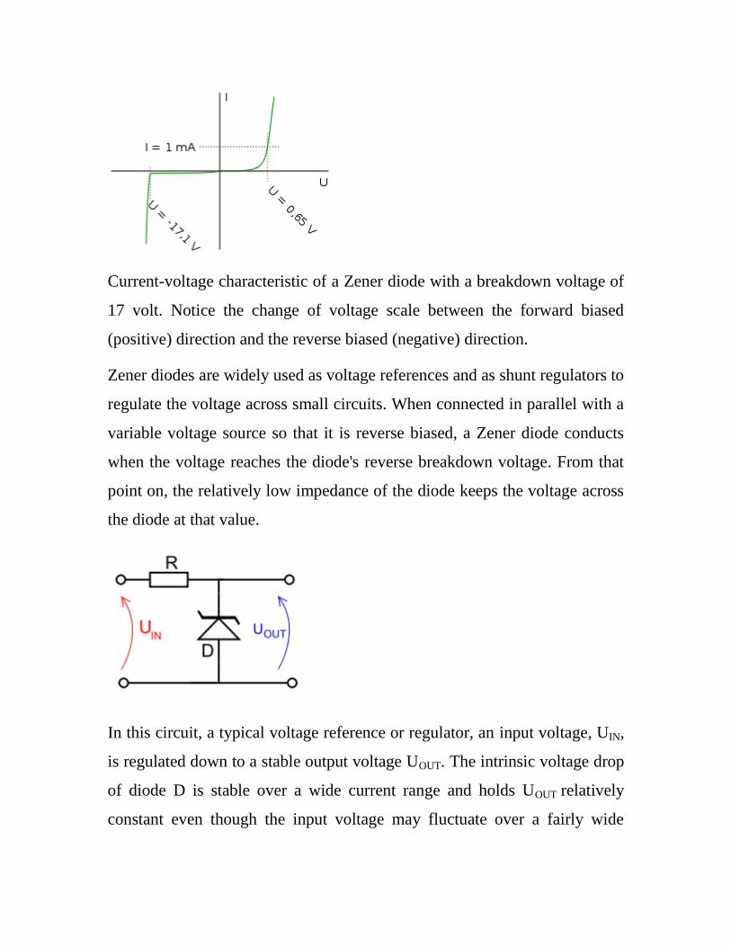
Current-voltage characteristic of a Zener diode with a breakdown voltage of
17 volt. Notice the change of voltage scale between the forward biased
(positive) direction and the reverse biased (negative) direction.
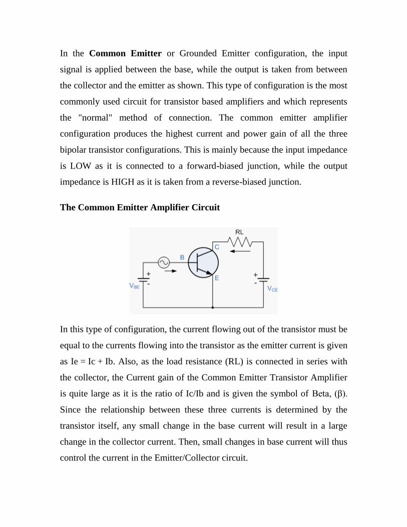
Zener diodes are widely used as voltage references and as shunt regulators to
regulate the voltage across small circuits. When connected in parallel with a
variable voltage source so that it is reverse biased, a Zener diode conducts
when the voltage reaches the diode's reverse breakdown voltage. From that
point on, the relatively low impedance of the diode keeps the voltage across
the diode at that value.
In this circuit, a typical voltage reference or regulator, an input voltage, UIN,
is regulated down to a stable output voltage UOUT. The intrinsic voltage drop
of diode D is stable over a wide current range and holds UOUT relatively
constant even though the input voltage may fluctuate over a fairly wide

range. Because of the low impedance of the diode when operated like this,
Resistor R is used to limit current through the circuit.
In the case of this simple reference, the current flowing in the diode is
determined using Ohms law and the known voltage drop across the resistor
R. IDiode = (UIN - UOUT) / RΩ
The value of R must satisfy two conditions:
1. R must be small enough that the current through D keeps D in reverse
breakdown. The value of this current is given in the data sheet for D.
For example, the common BZX79C5V6[2]
device, a 5.6 V 0.5 W
Zener diode, has a recommended reverse current of 5 mA. If
insufficient current exists through D, then UOUT will be unregulated,
and less than the nominal breakdown voltage (this differs to voltage
regulator tubes where the output voltage will be higher than nominal
and could rise as high as UIN). When calculating R, allowance must be
made for any current through the external load, not shown in this
diagram, connected across UOUT.
2. R must be large enough that the current through D does not destroy
the device. If the current through D is ID, its breakdown
voltage VB and its maximum power dissipation PMAX,
then IDVB < PMAX.
A load may be placed across the diode in this reference circuit, and as long
as the zener stays in reverse breakdown, the diode will provide a stable
voltage source to the load.
Shunt regulators are simple, but the requirements that the ballast resistor be

small enough to avoid excessive voltage drop during worst-case operation
(low input voltage concurrent with high load current) tends to leave a lot of
current flowing in the diode much of the time, making for a fairly wasteful
regulator with high quiescent power dissipation, only suitable for smaller
loads.
Zener diodes in this configuration are often used as stable references for
more advanced voltage regulator circuits.
These devices are also encountered, typically in series with a base-emitter
junction, in transistor stages where selective choice of a device centered
around the avalanche/Zener point can be used to introduce compensating
temperature co-efficient balancing of the transistor PN junction. An example
of this kind of use would be a DC error amplifier used in a regulated power
supply circuit feedback loop system.
Zener diodes are also used in surge protectors to limit transient voltage
spikes.
Another notable application of the zener diode is the use of noise caused by
its avalanche breakdown in a random number generator that never repeats.
Bipolar Transistor Basics
In the Diode tutorials we saw that simple diodes are made up from two
pieces of semiconductor material, either Silicon or Germanium to form a
simple PN-junction and we also learnt about their properties and
characteristics. If we now join together two individual diodes end to end
giving two PN-junctions connected together in series, we now have a three
layer, two junction, three terminal device forming the basis of a Bipolar
Junction Transistor, or BJT for short. This type of transistor is generally

known as a Bipolar Transistor, because its basic construction consists of
two PN-junctions with each terminal or connection being given a name to
identify it and these are known as the Emitter, Base and Collector
respectively.
The word Transistor is an acronym, and is a combination of the words
Transfer Varistor used to describe their mode of operation way back in their
early days of development. There are two basic types of bipolar transistor
construction, NPN and PNP, which basically describes the physical
arrangement of the P-type and N-type semiconductor materials from which
they are made. Bipolar Transistors are "CURRENT" Amplifying or current
regulating devices that control the amount of current flowing through them
in proportion to the amount of biasing current applied to their base terminal.
The principle of operation of the two transistor types NPN and PNP, is
exactly the same the only difference being in the biasing (base current) and
the polarity of the power supply for each type.
Bipolar Transistor Construction

The construction and circuit symbols for both the NPN and PNP bipolar
transistor are shown above with the arrow in the circuit symbol always
showing the direction of conventional current flow between the base
terminal and its emitter terminal, with the direction of the arrow pointing
from the positive P-type region to the negative N-type region, exactly the
same as for the standard diode symbol.
There are basically three possible ways to connect a Bipolar Transistor
within an electronic circuit with each method of connection responding
differently to its input signal as the static characteristics of the transistor vary
with each circuit arrangement.

1. Common Base Configuration - has Voltage Gain but no Current
Gain.
2. Common Emitter Configuration - has both Current and Voltage
Gain.
3. Common Collector Configuration - has Current Gain but no
Voltage Gain.
The Common Base Configuration.
As its name suggests, in the Common Base or Grounded Base
configuration, the BASE connection is common to both the input signal
AND the output signal with the input signal being applied between the base
and the emitter terminals. The corresponding output signal is taken from
between the base and the collector terminals as shown with the base terminal
grounded or connected to a fixed reference voltage point. The input current
flowing into the emitter is quite large as its the sum of both the base current
and collector current respectively therefore, the collector current output is
less than the emitter current input resulting in a Current Gain for this type of
circuit of less than "1", or in other words it "Attenuates" the signal.
The Common Base Amplifier Circuit

This type of amplifier configuration is a non-inverting voltage amplifier
circuit, in that the signal voltages Vin and Vout are In-Phase. This type of
arrangement is not very common due to its unusually high voltage gain
characteristics. Its Output characteristics represent that of a forward biased
diode while the Input characteristics represent that of an illuminated photo-
diode. Also this type of configuration has a high ratio of Output to Input
resistance or more importantly "Load" resistance (RL) to "Input" resistance
(Rin) giving it a value of "Resistance Gain". Then the Voltage Gain for a
common base can therefore be given as:
Common Base Voltage Gain
The Common Base circuit is generally only used in single stage amplifier
circuits such as microphone pre-amplifier or RF radio amplifiers due to its
very good high frequency response.
The Common Emitter Configuration.
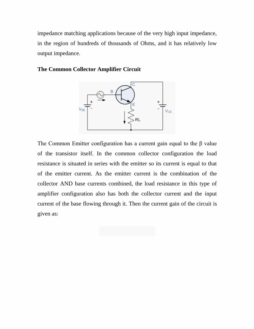
In the Common Emitter or Grounded Emitter configuration, the input
signal is applied between the base, while the output is taken from between
the collector and the emitter as shown. This type of configuration is the most
commonly used circuit for transistor based amplifiers and which represents
the "normal" method of connection. The common emitter amplifier
configuration produces the highest current and power gain of all the three
bipolar transistor configurations. This is mainly because the input impedance
is LOW as it is connected to a forward-biased junction, while the output
impedance is HIGH as it is taken from a reverse-biased junction.
The Common Emitter Amplifier Circuit
In this type of configuration, the current flowing out of the transistor must be
equal to the currents flowing into the transistor as the emitter current is given
as Ie = Ic + Ib. Also, as the load resistance (RL) is connected in series with
the collector, the Current gain of the Common Emitter Transistor Amplifier
is quite large as it is the ratio of Ic/Ib and is given the symbol of Beta, (β).
Since the relationship between these three currents is determined by the
transistor itself, any small change in the base current will result in a large
change in the collector current. Then, small changes in base current will thus
control the current in the Emitter/Collector circuit.

By combining the expressions for both Alpha, α and Beta, β the
mathematical relationship between these parameters and therefore the
current gain of the amplifier can be given as:
Where: "Ic" is the current flowing into the collector terminal, "Ib" is the
current flowing into the base terminal and "Ie" is the current flowing out of
the emitter terminal.
Then to summarise, this type of bipolar transistor configuration has a greater
input impedance, Current and Power gain than that of the common Base
configuration but its Voltage gain is much lower. The common emitter is an
inverting amplifier circuit resulting in the output signal being 180o out of
phase with the input voltage signal.
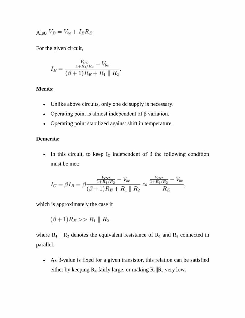
The Common Collector Configuration.
In the Common Collector or Grounded Collector configuration, the
collector is now common and the input signal is connected to the Base,
while the output is taken from the Emitter load as shown. This type of
configuration is commonly known as a Voltage Follower or Emitter
Follower circuit. The Emitter follower configuration is very useful for
impedance matching applications because of the very high input impedance,
in the region of hundreds of thousands of Ohms, and it has relatively low
output impedance.
The Common Collector Amplifier Circuit
The Common Emitter configuration has a current gain equal to the β value
of the transistor itself. In the common collector configuration the load
resistance is situated in series with the emitter so its current is equal to that
of the emitter current. As the emitter current is the combination of the
collector AND base currents combined, the load resistance in this type of
amplifier configuration also has both the collector current and the input
current of the base flowing through it. Then the current gain of the circuit is
given as:

This type of bipolar transistor configuration is a non-inverting amplifier
circuit in that the signal voltages of Vin and Vout are "In-Phase". It has a
voltage gain that is always less than "1" (unity). The load resistance of the
common collector amplifier configuration receives both the base and
collector currents giving a large current gain (as with the Common Emitter
configuration) therefore, providing good current amplification with very
little voltage gain.
Bipolar Transistor Summary.
The behaviour of the bipolar transistor in each one of the above circuit
configurations is very different and produces different circuit characteristics
with regards to Input impedance, Output impedance and Gain and this is
summarised in the table below.
Transistor Characteristics
The static characteristics for Bipolar Transistor amplifiers can be divided
into the following main groups.

Input Characteristics:- Common Base - IE ÷ VEB
Common
Emitter - IB ÷ VBE
Output
Characteristics:- Common Base - IC ÷ VC
Common
Emitter - IC ÷ VC
Transfer
Characteristics:- Common Base - IE ÷ IC
Common
Emitter - IB ÷ IC
with the characteristics of the different transistor configurations given in the
following table:
Characteristic Common
Base
Common
Emitter
Common
Collector
Input impedance Low Medium High
Output impedance Very High High Low
Phase Angle 0o 180
o 0
o
Voltage Gain High Medium Low
Current Gain Low Medium High
Power Gain Low Very High

Transistor as a switch
BJT used as an electronic switch, in grounded-emitter configuration.
Transistors are commonly used as electronic switches, for both high power
applications including switched-mode power supplies and low power
applications such as logic gates.
In a grounded-emitter transistor circuit, such as the light-switch circuit
shown, as the base voltage rises the base and collector current rise
exponentially, and the collector voltage drops because of the collector load
resistor. The relevant equations:
VRC = ICE × RC, the voltage across the load (the lamp with resistance
RC)
VRC + VCE = VCC, the supply voltage shown as 6V
If VCE could fall to 0 (perfect closed switch) then Ic could go no higher than
VCC / RC, even with higher base voltage and current. The transistor is then
said to be saturated. Hence, values of input voltage can be chosen such that
the output is either completely off,[13]
or completely on. The transistor is
acting as a switch, and this type of operation is common in digital circuits
where only "on" and "off" values are relevant.

Transistor as an amplifier
Amplifier circuit, standard common-emitter configuration.
The common-emitter amplifier is designed so that a small change in voltage
in (Vin) changes the small current through the base of the transistor and the
transistor's current amplification combined with the properties of the circuit
mean that small swings in Vin produce large changes in Vout.
Various configurations of single transistor amplifier are possible, with some
providing current gain, some voltage gain, and some both.
From mobile phones to televisions, vast numbers of products include
amplifiers for sound reproduction, radio transmission, and signal processing.
The first discrete transistor audio amplifiers barely supplied a few hundred
milliwatts, but power and audio fidelity gradually increased as better
transistors became available and amplifier architecture evolved.
Modern transistor audio amplifiers of up to a few hundred watts are common
and relatively inexpensive
Voltage divider bias

Voltage divider bias
The voltage divider is formed using external resistors R1 and R2. The voltage
across R2 forward biases the emitter junction. By proper selection of
resistors R1 and R2, the operating point of the transistor can be made
independent of β. In this circuit, the voltage divider holds the base voltage
fixed independent of base current provided the divider current is large
compared to the base current. However, even with a fixed base voltage,
collector current varies with temperature (for example) so an emitter resistor
is added to stabilize the Q-point, similar to the above circuits with emitter
resistor.
In this circuit the base voltage is given by:
voltage across
provided .
Also
For the given circuit,
Merits:
Unlike above circuits, only one dc supply is necessary.
Operating point is almost independent of β variation.
Operating point stabilized against shift in temperature.
Demerits:
In this circuit, to keep IC independent of β the following condition
must be met:
which is approximately the case if
where R1 || R2 denotes the equivalent resistance of R1 and R2 connected in
parallel.
As β-value is fixed for a given transistor, this relation can be satisfied
either by keeping RE fairly large, or making R1||R2 very low.

If RE is of large value, high VCC is necessary. This increases
cost as well as precautions necessary while handling.
If R1 || R2 is low, either R1 is low, or R2 is low, or both are low.
A low R1 raises VB closer to VC, reducing the available swing in
collector voltage, and limiting how large RC can be made
without driving the transistor out of active mode. A low R2
lowers Vbe, reducing the allowed collector current. Lowering
both resistor values draws more current from the power supply
and lowers the input resistance of the amplifier as seen from the
base.
AC as well as DC feedback is caused by RE, which reduces the AC
voltage gain of the amplifier. A method to avoid AC feedback while
retaining DC feedback is discussed below.
Base Bias
The simplest biasing applies a base-bias resistor between the base and a base
battery VBB. It is convenient to use the existing VCC supply instead of a new
bias supply. An example of an audio amplifier stage using base-biasing is
―Crystal radio with one transistor . . . ‖ crystal radio, Ch 9 . Note the resistor
from the base to the battery terminal. A similar circuit is shown in Figure
below.
Write a KVL (Krichhoff's voltage law) equation about the loop containing
the battery, RB, and the VBE diode drop on the transistor in Figure below.
Note that we use VBB for the base supply, even though it is actually VCC. If β
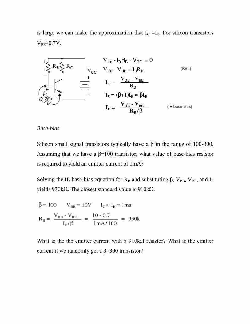
is large we can make the approximation that IC =IE. For silicon transistors
VBE≅0.7V.
Base-bias
Silicon small signal transistors typically have a β in the range of 100-300.
Assuming that we have a β=100 transistor, what value of base-bias resistor
is required to yield an emitter current of 1mA?
Solving the IE base-bias equation for RB and substituting β, VBB, VBE, and IE
yields 930kΩ. The closest standard value is 910kΩ.
What is the the emitter current with a 910kΩ resistor? What is the emitter
current if we randomly get a β=300 transistor?
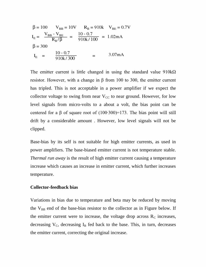
The emitter current is little changed in using the standard value 910kΩ
resistor. However, with a change in β from 100 to 300, the emitter current
has tripled. This is not acceptable in a power amplifier if we expect the
collector voltage to swing from near VCC to near ground. However, for low
level signals from micro-volts to a about a volt, the bias point can be
centered for a β of square root of (100·300)=173. The bias point will still
drift by a considerable amount . However, low level signals will not be
clipped.
Base-bias by its self is not suitable for high emitter currents, as used in
power amplifiers. The base-biased emitter current is not temperature stable.
Thermal run away is the result of high emitter current causing a temperature
increase which causes an increase in emitter current, which further increases
temperature.
Collector-feedback bias
Variations in bias due to temperature and beta may be reduced by moving
the VBB end of the base-bias resistor to the collector as in Figure below. If
the emitter current were to increase, the voltage drop across RC increases,
decreasing VC, decreasing IB fed back to the base. This, in turn, decreases
the emitter current, correcting the original increase.

Write a KVL equation about the loop containing the battery, RC , RB , and
the VBE drop. Substitute IC≅IE and IB≅IE/β. Solving for IE yields the IE CFB-
bias equation. Solving for IB yields the IB CFB-bias equation.
Collector-feedback bias.
Find the required collector feedback bias resistor for an emitter current of 1
mA, a 4.7K collector load resistor, and a transistor with β=100 . Find the
collector voltage VC. It should be approximately midway between VCC and
ground.
The closest standard value to the 460k collector feedback bias resistor is
470k. Find the emitter current IE with the 470 K resistor. Recalculate the
emitter current for a transistor with β=100 and β=300.

We see that as beta changes from 100 to 300, the emitter current increases
from 0.989mA to 1.48mA. This is an improvement over the previous base-
bias circuit which had an increase from 1.02mA to 3.07mA. Collector
feedback bias is twice as stable as base-bias with respect to beta variation.
Emitter-bias
Inserting a resistor RE in the emitter circuit as in Figure below causes
degeneration, also known as negative feedback. This opposes a change in
emitter current IE due to temperature changes, resistor tolerances, beta
variation, or power supply tolerance. Typical tolerances are as follows:
resistor— 5%, beta— 100-300, power supply— 5%. Why might the emitter
resistor stabilize a change in current? The polarity of the voltage drop across
RE is due to the collector battery VCC. The end of the resistor closest to the (-
) battery terminal is (-), the end closest to the (+) terminal it (+). Note that
the (-) end of RE is connected via VBB battery and RB to the base. Any
increase in current flow through RE will increase the magnitude of negative
voltage applied to the base circuit, decreasing the base current, decreasing
the emitter current. This decreasing emitter current partially compensates the
original increase.

Emitter-bias
Note that base-bias battery VBB is used instead of VCC to bias the base in
Figure above. Later we will show that the emitter-bias is more effective with
a lower base bias battery. Meanwhile, we write the KVL equation for the
loop through the base-emitter circuit, paying attention to the polarities on the
components. We substitute IB≅IE/β and solve for emitter current IE. This
equation can be solved for RB , equation: RB emitter-bias, Figure above.
Before applying the equations: RB emitter-bias and IE emitter-bias, Figure
above, we need to choose values for RC and RE . RC is related to the collector
supply VCC and the desired collector current IC which we assume is
approximately the emitter current IE. Normally the bias point for VC is set to
half of VCC. Though, it could be set higher to compensate for the voltage
drop across the emitter resistor RE. The collector current is whatever we
require or choose. It could range from micro-Amps to Amps depending on
the application and transistor rating. We choose IC = 1mA, typical of a
small-signal transistor circuit. We calculate a value for RC and choose a
close standard value. An emitter resistor which is 10-50% of the collector
load resistor usually works well.
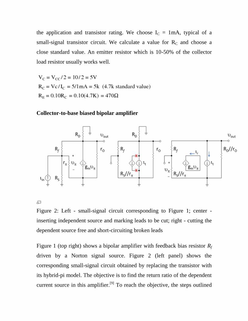
Collector-to-base biased bipolar amplifier
Figure 2: Left - small-signal circuit corresponding to Figure 1; center -
inserting independent source and marking leads to be cut; right - cutting the
dependent source free and short-circuiting broken leads
Figure 1 (top right) shows a bipolar amplifier with feedback bias resistor Rf
driven by a Norton signal source. Figure 2 (left panel) shows the
corresponding small-signal circuit obtained by replacing the transistor with
its hybrid-pi model. The objective is to find the return ratio of the dependent
current source in this amplifier.[9]
To reach the objective, the steps outlined

above are followed. Figure 2 (center panel) shows the application of these
steps up to Step 4, with the dependent source moved to the left of the
inserted source of value it, and the leads targeted for cutting marked with an
x. Figure 2 (right panel) shows the circuit set up for calculation of the return
ratio T, which is
The return current is
The feedback current in Rf is found by current division to be:
The base-emitter voltage vπ is then, from Ohm's law:
Consequently,
Application in asymptotic gain model
The overall transresistance gain of this amplifier can be shown to be:

with R1 = RS || rπ and R2 = RD || rO.
This expression can be rewritten in the form used by the asymptotic gain
model, which expresses the overall gain of a feedback amplifier in terms of
several independent factors that are often more easily derived separately
than the overall gain itself, and that often provide insight into the circuit.
This form is:
where the so-called asymptotic gain G∞ is the gain at infinite gm, namely:
and the so-called feed forward or direct feedthrough G0 is the gain for
zero gm, namely:
For additional applications of this method, see asymptotic gain model.
1. DC Biasing Circuits
2. The ac operation of an amplifier depends on the initial dc values of
IB, IC, and VCE.
3. By varying IB around an initial dc value, IC and VCE are made to
vary around their initial dc values.
4. DC biasing is a static operation since it deals with setting a fixed
(steady) level of current (through the device) with a desired fixed
voltage drop across the device.

Purpose of the DC biasing circuit
1. To turn the device ―ON‖
2. To place it in operation in the region of its characteristic where the
device operates most linearly, i.e. to set up the initial dc values of IB,
IC, and VCE
Voltage-Divider Bias
• The voltage – divider (or potentiometer) bias circuit is by far the most
commonly used.
RC
RB
+VCC
ic
vce
ib
vin
vout

RC
R1
+VCC
IC
IE
RE
R2
• RB1, RB2
voltage-divider to set the value of VB , IB
• C3
to short circuit ac signals to ground, while not effect the DC
operating (or biasing) of a circuit
(RE stabilizes the ac signals)
Bypass Capacitor
Graphical DC Bias Analysis
RC
R1
+VCC
RE
R2
vout
vin
C2C
1
C3

• The straight line is know as the DC load line
• Its significance is that regardless of the behavior of the transistor, the
collector current IC and the collector-emitter voltage VCE must
always lie on the load line, depends ONLY on the VCC, RC and RE
• (i.e. The dc load line is a graph that represents all the possible
combinations of IC and VCE for a given amplifier. For every
possible value of IC, and amplifier will have a corresponding value of
VCE.)
• It must be true at the same time as the transistor characteristic. Solve
two condition using simultaneous equation
graphically Q-point !!
cmxy
RR
VV
RRI
II
RIVRIV
EC
CC
CE
EC
C
EECECCCC
EC
:equation linestraight of form slope-Point
1
for
0
IC
(mA)
VCE
VCE(off)
= VCC
IC(sat)
= VCC
/(RC+R
E)
DC Load Line
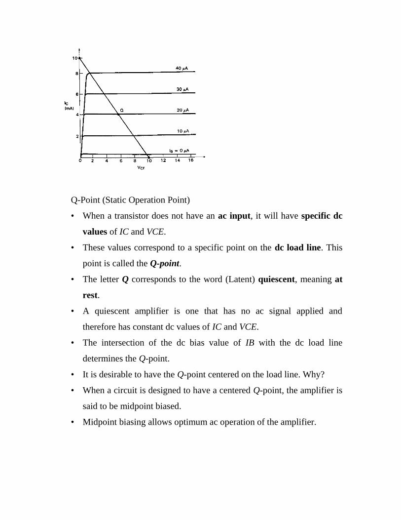
Q-Point (Static Operation Point)
• When a transistor does not have an ac input, it will have specific dc
values of IC and VCE.
• These values correspond to a specific point on the dc load line. This
point is called the Q-point.
• The letter Q corresponds to the word (Latent) quiescent, meaning at
rest.
• A quiescent amplifier is one that has no ac signal applied and
therefore has constant dc values of IC and VCE.
• The intersection of the dc bias value of IB with the dc load line
determines the Q-point.
• It is desirable to have the Q-point centered on the load line. Why?
• When a circuit is designed to have a centered Q-point, the amplifier is
said to be midpoint biased.
• Midpoint biasing allows optimum ac operation of the amplifier.

DC Biasing + AC signal
• When an ac signal is applied to the base of the transistor, IC and VCE
will both vary around their Q-point values.
• When the Q-point is centered, IC and VCE can both make the
maximum possible transitions above and below their initial dc values.
• When the Q-point is above the center on the load line, the input signal
may cause the transistor to saturate. When this happens, a part of the
output signal will be clipped off.
• When the Q-point is below midpoint on the load line, the input signal
may cause the transistor to cutoff. This can also cause a portion of the
output signal to be clipped.

DC and AC Equivalent Circuits
Bias Circuit DC equivalent circuit
AC equ ckt
RC
R1
+VCC
RE
R2
RL
vin
RC
R1
+VCC
IC
IE
RE
R2
R1//R
2
rCv
ce
rC = R
C//R
L
vin

• The ac load line of a given amplifier will not follow the plot of the dc
load line.
• This is due to the dc load of an amplifier is different from the ac load.
What does the ac load line tell you?
• The ac load line is used to tell you the maximum possible output
voltage swing for a given common-emitter amplifier.
• In other words, the ac load line will tell you the maximum possible
peak-to-peak output voltage (Vpp ) from a given amplifier.
• This maximum Vpp is referred to as the compliance of the amplifier.
(AC Saturation Current Ic(sat) , AC Cutoff Voltage VCE(off) )
IC
VCE
Q - point
ac load line
dc load line

Bias stabilization
The establishment of an operating point on the transistor volt-ampere
characteristics by means of direct voltages and currents.
Since the transistor is a three-terminal device, any one of the three terminals
may be used as a common terminal to both input and output. In most
transistor circuits the emitter is used as the common terminal, and this
common emitter, or grounded emitter, is indicated in illus. a. If the transistor
is to used as a linear device, such as an audio amplifier, it must be biased to
operate in the active region. In this region the collector is biased in the
reverse direction and the emitter in the forward direction. The area in the
common-emitter transistor characteristics to the right of the ordinate VCE = 0
and above IC = 0 is the active region. Two more biasing regions are of
special interest for those cases in which the transistor is intended to operate
as a switch. These are the saturation and cutoffregions. The saturation region
may be defined as the region where the collector current is independent of
base current for given values of VCC and RL. Thus, the onset of saturation can
be considered to take place at the knee of the common-emitter transistor
curves. See also Amplifier; Transistor.

Translator circuits. (a) Fixed-bias. (b) Collector-to-base bias. (c) Self-bias.
In saturation, the transistor current IC is nominally VCC/RL. Since RL is small,
it may be necessary to keep VCCcorrespondingly small in order to stay within
the limitations imposed by the transistor on maximum-current and collector-
power dissipation. In the cutoff region it is required that the emitter
current IE be zero, and to accomplish this it is necessary to reverse-bias
the emitter junction so that the collector current is approximately equal to
thereverse saturation current ICO. A reverse-biasing voltage of the order of
0.1 V across the emitter junction willordinarily be adequate to cut off either
a germanium or silicon transistor.
The particular method to be used in establishing an operating point on the
transistor characteristics depends on whether the transistor is to operate in
the active, saturation or cutoff regions; on the application under
consideration; on the thermal stability of the circuit; and on other factors.

In a fixed-bias circuit, the operating point for the circuit of illus. a can be
established by noting that the required current IB is constant, independent of
the quiescent collector current IC, which is why this circuit is called the
fixed-bias circuit. Transistor biasing circuits are frequently compared in
terms of the value of the stability factor S = ∂IC/∂ICO, which is the rate of
change of collector current with respect to reverse saturation current. The
smaller the value of S, the less likely the circuit will exhibit thermal
runaway. S, as defined here, cannot be smaller than unity. Other stability
factors are defined in terms of dc current gain hFE as ∂IC/∂hFE, and in terms
of base-to-emitter voltage as ∂IC/∂VBE. However, bias circuits with small
values of S will also perform satisfactorily for transistors that have large
variations of hFE and VBE. For the fixed-bias circuit it can be shown
that S = hFE + 1, and if hFE = 50, thenS = 51. Such a large value of S makes
thermal runaway a definite possibility with this circuit.
In collector-to-base bias, an improvement in stability is obtained if
the resistor RB in illus. a is returned to the collector junction rather than to
the battery terminal. Such a connection is shown in illus. b. In this bias
circuit, if ICtends to increase (either because of a rise in temperature or
because the transistor has been replaced by another), then VCE decreases.
Hence IB also decreases and, as a consequence of this lowered bias current,
the collector current is not allowed to increase as much as it would if fixed
bias were used. The stability factor S is shown in Eq. (1).
1.
This value is smaller than hFE + 1, which is the value obtained for the fixed-
bias case.

If the load resistance RL is very small, as in a transformer-coupled circuit,
then the previous expression for S shows that there would be no
improvement in the stabilization in the collector-to-base bias circuit over the
fixed-bias circuit. A circuit that can be used even if there is zero dc
resistance in series with the collector terminal is the self-biasing
configuration of illus. c. The current in the resistance RE in the emitter lead
causes a voltage drop which is in the direction to reverse-bias the emitter
junction. Since this junction must be forward-biased (for active region bias),
the bleeder R1-R2 has been added to the circuit.
If IC tends to increase, the current in RE increases. As a consequence of the
increase in voltage drop across RE, the base current is decreased.
Hence IC will increase less than it would have had there been no self-biasing
resistor RE. The stabilization factor for the self-bias circuit is shown by Eq.
(2), where RB = R1R2/(R1 + R2). The smaller the value of RB, the
2.
better the stabilization. Even if RB approaches zero, the value of S cannot be
reduced below unity.
In order to avoid the loss of signal gain because of the degeneration caused
by RE, this resistor is often bypassed by a very large capacitance, so that
its reactance at the frequencies under consideration is very small.
The selection of an appropriate operating point (ID, VGS, VDS) for a field-
effect transistor (FET) amplifier stage is determined by considerations
similar to those given to transistors, as discussed previously. These
considerations are output-voltage swing, distortion, power dissipation,

voltage gain, and drift of drain current. In most cases it is not possible to
satisfy all desired specifications simultaneously.
Question Bank
PART –A
1.what is barrier potential?
2. Define biasing.
PART-B
1.(a) Explain the working of varactor diode.
(b) What does a DC load line represent? May this line be used when an AC signal is
applied? When it is necessary to draw an AC load line?
2.(a) Explain the input and output characteristics of a transistor in common emitter
configuration with neat diagram.
(b) Explain how the zener diode acts as a voltage regulator with relevant diagram.

UNIT II
FET, UJT AND SCR
JFET characteristics and parameters – JFET biasing – Self bias – Voltage divider bias –
Q point – Stability over temperature – MOSFET – D-MOSFET and E-MOSFET –
MOSFET characteristics and parameters – MOSFET biasing – Zero bias – Voltage
divider bias – Drain feedback bias – Characteristics and applications of UJT, SCR,
DIAC, TRIAC.
UNIT II
FET, UJT AND SCR
The Common Source JFET Amplifier
So far we have looked at the bipolar type transistor amplifier and especially
the common emitter amplifier, but small signal amplifiers can also be made
using Field Effect Transistors or FET's for short. These devices have the
advantage over bipolar transistors of having an extremely high input
impedance along with a low noise output making them ideal for use in
amplifier circuits that have very small input signals. The design of an
amplifier circuit based around a junction field effect transistor or "JFET", (n-
channel FET for this tutorial) or even a metal oxide silicon FET or
"MOSFET" is exactly the same principle as that for the bipolar transistor
circuit used for a Class A amplifier circuit we looked at in the previous
tutorial. Firstly, a suitable quiescent point or "Q-point" needs to be found for
the correct biasing of the JFET amplifier circuit with single amplifier
configurations of Common-source (CS), Common-drain (CD) or Source-
follower (SF) and the Common-gate (CG) available for most FET devices.
These three JFET amplifier configurations correspond to the common-
emitter, emitter-follower and the common-base configurations using bipolar
transistors. In this tutorial we will look at the Common Source JFET
Amplifier as this is the most widely used JFET amplifier design. Then
consider the common source JFET amplifier circuit below.
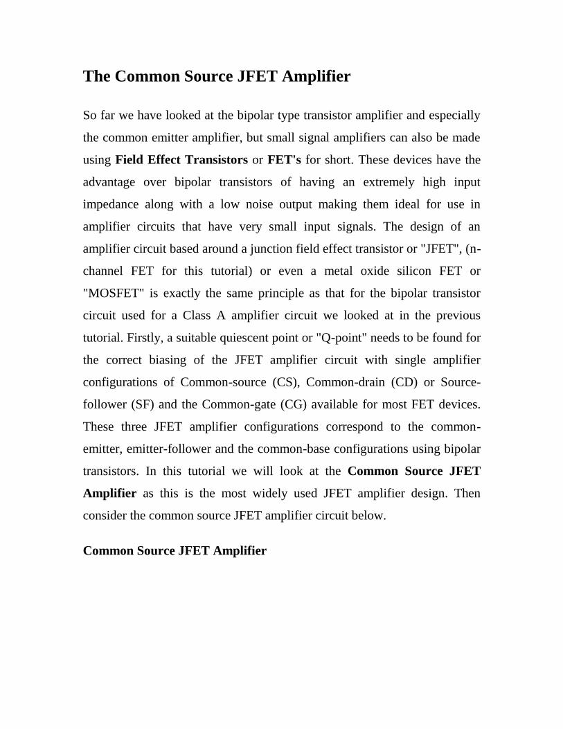
Common Source JFET Amplifier
The amplifier circuit consists of an N-channel JFET, but the device could
also be an equivalent N-channel depletion-mode MOSFET as the circuit
diagram would be the same just a change in the FET, connected in a
common source configuration. The JFET gate voltage Vg is biased through
the potential divider network set up by resistors R1 and R2 and is biased to
operate within its saturation region which is equivalent to the active region
of the bipolar junction transistor. Unlike a bipolar transistor circuit, the
junction FET takes virtually no input gate current allowing the gate to be
treated as an open circuit. Then no input characteristics curves are required.
We can compare the JFET to the bipolar junction transistor (BJT) in the
following table.
JFET to BJT Comparison
JFET BJT
Gate, (G) Base, (B)
Drain, (D) Collector, (C)
Source, (S) Emitter, (E)

Gate Supply, (Vg) Base Supply, (VB)
Drain Supply,
(VDD)
Collector Supply,
(VCC)
Drain Current,
(iD)
Collector Current,
(iC)
Since the N-Channel JFET is a depletion mode device and is normally
"ON", a negative gate voltage with respect to the source is required to
modulate or control the drain current. This negative voltage can be provided
by biasing from a separate power supply voltage or by a self biasing
arrangement as long as a steady current flows through the JFET even when
there is no input signal present and Vg maintains a reverse bias of the gate-
source pn junction. In this example the biasing is provided from a potential
divider network allowing the input signal to produce a voltage fall at the gate
as well as voltage rise at the gate with a sinusoidal signal. Any suitable pair
of resistor values in the correct proportions would produce the correct
biasing voltage so the DC gate biasing voltage Vg is given as:
Note that this equation only determines the ratio of the resistors R1 and R2,
but in order to take advantage of the very high input impedance of the JFET
as well as reducing the power dissipation within the circuit, we need to make
these resistor values as high as possible, with values in the order of 1 to
10MΩ being common.

The input signal, (Vin) of the common source JFET amplifier is applied
between the Gate terminal and the zero volts rail, (0v). With a constant value
of gate voltage Vg applied the JFET operates within its "Ohmic region"
acting like a linear resistive device. The drain circuit contains the load
resistor, Rd. The output voltage, Vout is developed across this load
resistance. The efficiency of the common source JFET amplifier can be
improved by the addition of a resistor, Rs included in the source lead with
the same drain current flowing through this resistor. Resistor, Rs is also used
to set the JFET amplifiers "Q-point".
When the JFET is switched fully "ON" a voltage drop equal to Rs x Id is
developed across this resistor raising the potential of the source terminal
above 0v or ground level. This voltage drop across Rs due to the drain
current provides the necessary reverse biasing condition across the gate
resistor, R2 effectively generating negative feedback. In order to keep the
gate-source junction reverse biased, the source voltage, Vs needs to be
higher than the gate voltage, Vg. This source voltage is therefore given as:
Then the Drain current, Id is also equal to the Source current, Is as "No
Current" enters the Gate terminal and this can be given as:
This potential divider biasing circuit improves the stability of the common
source JFET amplifier circuit when being fed from a single DC supply
compared to that of a fixed voltage biasing circuit. Both resistor, Rs and the
source by-pass capacitor, Cs serve basically the same function as the emitter
resistor and capacitor in the common emitter bipolar transistor amplifier
circuit, namely to provide good stability and prevent a reduction in the loss
of the voltage gain. However, the price paid for a stabilized quiescent gate
voltage is that more of the supply voltage is dropped across Rs.
The the value in farads of the source by-pass capacitor is generally fairly
high above 100uF and will be polarized. This gives the capacitor an
impedance value much smaller, less than 10% of the transconductance, gm
(the transfer coefficient representing gain) value of the device. At high
frequencies the by-pass capacitor acts essentially as a short-circuit and the
source will be effectively connected directly to ground.
The basic circuit and characteristics of a Common Source JFET Amplifier
are very similar to that of the common emitter amplifier. A DC load line is
constructed by joining the two points relating to the drain current, Id and the
supply voltage, Vdd remembering that when Id = 0: ( Vdd = Vds ) and when
Vds = 0: ( Id = Vdd/RL ). The load line is therefore the intersection of the
curves at the Q-point as follows.
Common Source JFET Amplifier Characteristics Curves

As with the common emitter bipolar circuit, the DC load line for the
common source JFET amplifier produces a straight line equation whose
gradient is given as: -1/(Rd + Rs) and that it crosses the vertical Id axis at
point A equal to Vdd/(Rd + Rs). The other end of the load line crosses the
horizontal axis at point B which is equal to the supply voltage, Vdd. The
actual position of the Q-point on the DC load line is generally positioned at
the mid centre point of the load line (for class-A operation) and is
determined by the mean value of Vg which is biased negatively as the JFET
is a depletion-mode device. Like the bipolar common emitter amplifier the

output of the Common Source JFET Amplifier is 180o out of phase with
the input signal.
One of the main disadvantages of using Depletion-mode JFET is that they
need to be negatively biased. Should this bias fail for any reason the gate-
source voltage may rise and become positive causing an increase in drain
current resulting in failure of the drain voltage, Vd. Also the high channel
resistance, Rds(on) of the junction FET, coupled with high quiescent steady
state drain current makes these devices run hot so additional heatsink is
required. However, most of the problems associated with using JFET's can
be greatly reduced by using enhancement-mode MOSFET devices instead.
We know that controlling the Q point of our JFET is more difficult than it
was with our junction transistor. This is because IDSS varies widely from
one JFET to the next. In order to stabilize I to a constant level from one
JFET to another, we need a circuit that will vary
VGSwidely.
Gate bias
is the simplest but worst way to control the drain current.With gate bias, we
supply a constant value of V , and the resulting drain current will vary
widely from device to device.
Self bias
offers some improvement because the source resistor produces local
feedback. Here, the value
of V varies somewhat with the value of drain current. This helps to control
the drain current.
Voltage Divider bias

results in a relatively stable Q point, however, it requires a large supply
voltage.
Gate Bias
1) With gate bias, you apply a fixed gate voltage that reverse biases
the gate of the JFET. This produces a drain current that is less than I .
The problem is that you cannot accurately predict the drain current in mass
production because of the variation in the required V .
The following will illustrate this point.
2) Build the circuit shown in Figure 3. Apply a V of -1.5V.
Measure V , I , and V . and record the data in Table 2 for each JFET.
Self Bias
Build the circuit shown in Figure 4. Measure and record the 3 values shown
in Table 3. Repeat the measurements for the other JFETs.
The drain current variation for the self- bias circuit should be less than
the
variation than the gate-biased circuit.

Voltage Divider Bias
Build the circuit shown in Figure 5. Measure and record the 3 values shown
in Table 4. Repeat the measurements for the other JFET.
The drain current variation for the voltage divider bias circuit should
continue to become more stable. It should show less variation than either
of the circuits above.

Q-Point
the bias point is chosen to keep the transistor operating in the active mode,
using a variety of circuit techniques, establishing the Q-point DC voltage
and current. A small signal is then applied on top of the Q-point bias
voltage, thereby either modulating or switching the current, depending on
the purpose of the circuit.
The quiescent point of operation is typically near the middle of DC load line.
The process of obtaining certain DC collector current at a certain DC
collector voltage by setting up operating point is called biasing.
After establishing the operating point, when input signal is applied, the
output signal should not move the transistor either to saturation or to cut-off.
However, this unwanted shift still might occur, due to the following reasons:
1. Parameters of transistors depend on junction temperature. As junction
temperature increases, leakage current due to minority charge carriers
(ICBO) increases. As ICBO increases, ICEO also increases, causing an
increase in collector current IC. This produces heat at the collector
junction. This process repeats, and, finally, Q-point may shift into the
saturation region. Sometimes, the excess heat produced at the junction
may even burn the transistor. This is known as thermal runaway.
2. When a transistor is replaced by another of the same type, the Q-point
may shift, due to changes in parameters of the transistor, such
as current gain (β) which varies slightly for each unique transistor.

To avoid a shift of Q-point, bias-stabilization is necessary. Various biasing
circuits can be used for this purpose.
MOSFETs or Metal Oxide Semiconductor FET's have much higher input
impedances and low channel resistances compared to the equivalent JFET.
Also the biasing arrangements for MOSFETs are different and unless we
bias them positively for N-channel devices and negatively for P-channel
devices no drain current will flow, then we have in effect a fail safe
transistor.
A Power MOSFET is a specific type of metal oxide semiconductor field-
effect transistor (MOSFET) designed to handle large amounts of power.
Compared to the other power semiconductor devices (IGBT, Thyristor...), its
main advantages are high commutation speed and good efficiency at low
voltages. It shares with the IGBT an isolated gate that makes it easy to drive.
It was made possible by the evolution of CMOS technology, developed for
manufacturing Integrated circuits in the late 1970s. The power MOSFET
shares its operating principle with its low-power counterpart, the lateral
MOSFET.
The power MOSFET is the most widely used low-voltage (i.e. less
than 200 V) switch. It can be found in most power supplies, DC to DC
converters, and low voltage motor controllers.
Basic structure
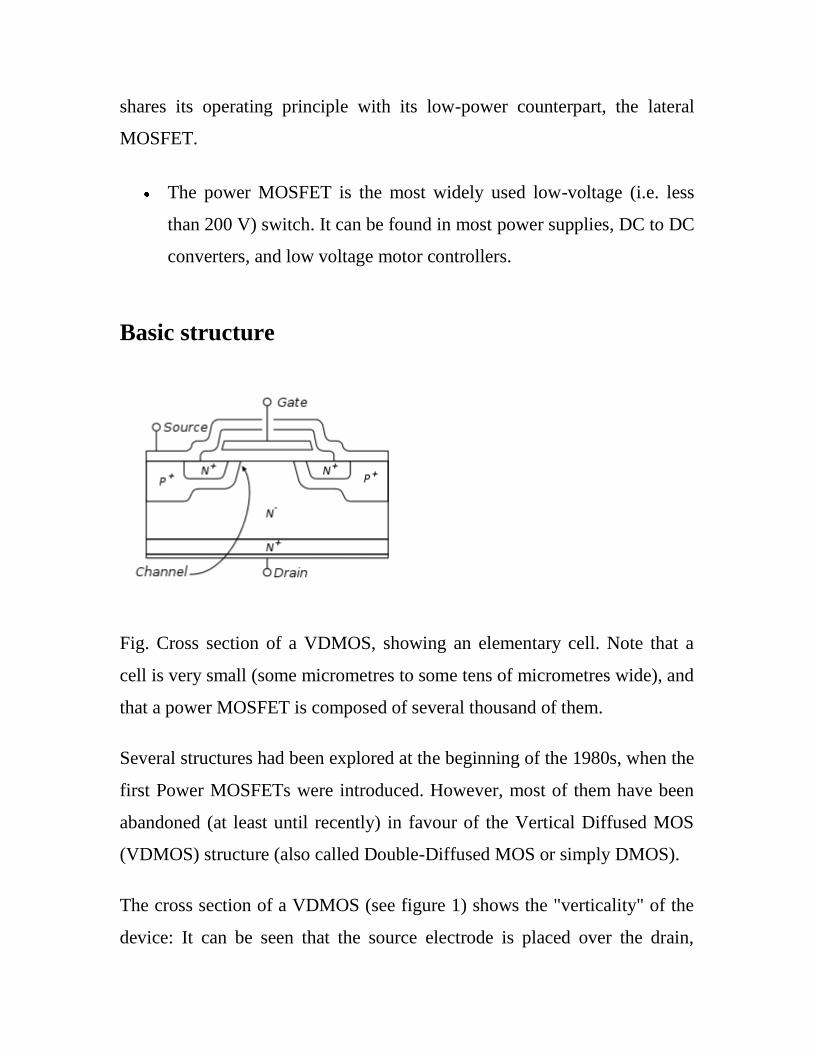
Fig. Cross section of a VDMOS, showing an elementary cell. Note that a
cell is very small (some micrometres to some tens of micrometres wide), and
that a power MOSFET is composed of several thousand of them.
Several structures had been explored at the beginning of the 1980s, when the
first Power MOSFETs were introduced. However, most of them have been
abandoned (at least until recently) in favour of the Vertical Diffused MOS
(VDMOS) structure (also called Double-Diffused MOS or simply DMOS).
The cross section of a VDMOS (see figure 1) shows the "verticality" of the
device: It can be seen that the source electrode is placed over the drain,

resulting in a current mainly vertical when the transistor is in the on-state.
The "diffusion" in VDMOS refers to the manufacturing process: the P wells
are obtained by a diffusion process (actually a double diffusion process to
get the P and N+ regions, hence the name double diffused).
Power MOSFETs have a different structure than the lateral MOSFET: as
with all power devices, their structure is vertical and not planar. In a planar
structure, the current and breakdown voltage ratings are both functions of
the channel dimensions (respectively width and length of the channel),
resulting in inefficient use of the "silicon estate". With a vertical structure,
the voltage rating of the transistor is a function of the doping and thickness
of the N epitaxial layer (see cross section), while the current rating is a
function of the channel width. This makes possible for the transistor to
sustain both high blocking voltage and high current within a compact piece
of silicon.
It is worth noting that power MOSFETs with lateral structure exist. They are
mainly used in high-end audio amplifiers. Their advantage is a better
behaviour in the saturated region (corresponding to the linear region of a
bipolar transistor) than the vertical MOSFETs. Vertical MOSFETs are
designed for switching applications, so they are only used in On or Off
states.
-

State characteristics
On-state resistance
Contribution of the different parts of the MOSFET to the on-state resistance.
When the power MOSFET is in the on-state (see MOSFET for a discussion
on operation modes), it exhibits a resistive behaviour between the drain and
source terminals. It can be seen in figure 2 that this resistance (called RDSon
for "drain to source resistance in on-state") is the sum of many elementary
contributions:
RS is the source resistance. It represents all resistances between the
source terminal of the package to the channel of the MOSFET:
resistance of the wire bonds, of the source metallisation, and of the N+
wells;
Rch. This is the channel resistance. It is inversely proportional to the
channel width, and for a given die size, to the channel density. The
channel resistance is one of the main contributors to the RDSon of low-
voltage MOSFETs, and intensive work has been carried out to reduce
their cell size in order to increase the channel density;

Ra is the access resistance. It represents the resistance of the epitaxial
zone directly under the gate electrode, where the direction of the
current changes from horizontal (in the channel) to vertical (to the
drain contact);
RJFET is the detrimental effect of the cell size reduction mentioned
above: the P implantations form the gates of a parasitic JFET
transistor that tend to reduce the width of the current flow;
Rn is the resistance of the epitaxial layer. As the role of this layer is to
sustain the blocking voltage, Rn is directly related to the voltage rating
of the device. A high voltage MOSFET requires a thick, low-doped
layer (i.e. highly resistive), whereas a low-voltage transistor only
requires a thin layer with a higher doping level (i.e. less resistive). As
a result, Rn is the main factor responsible for the resistance of high-
voltage MOSFETs;
RD is the equivalent of RS for the drain. It represents the resistance of
the transistor substrate (note that the cross section in figure is not at
scale, the bottom N+ layer is actually the thickest) and of the package
connections.
Breakdown voltage/on-state resistance trade-off

The RDSon of the MOSFETs increase with their Voltage rating.
When in the OFF-state, the power MOSFET is equivalent to a PIN diode
(constituted by the P + diffusion, the N
- epitaxial layer and the N
+ substrate).
When this highly non-symmetrical structure is reverse-biased, the space-
charge region extends principally on the light-doped side, i.e over the N-
layer. This means that this layer has to withstand most of the MOSFET's
OFF-state drain-to-source voltage.
However, when the MOSFET is in the ON-state, this N- layer has no
function. Furthermore, as it is a lightly-doped region, its intrinsic resistivity
is non-negligible and adds to the MOSFET's ON-state Drain-to-Source
Resistance (RDSon) (this is the Rn resistance in figure).
Two main parameters govern both the breakdown voltage and the RDSon of
the transistor: the doping level and the thickness of the N- epitaxial layer.
The thicker the layer and the lower its doping level, the higher the
breakdown voltage. On the contrary, the thinner the layer and the higher the
doping level, the lower the RDSon (and therefore the lower the conduction
losses of the MOSFET). Therefore, it can be seen that there is a trade-off in
the design of a MOSFET, between its voltage rating and its ON-state
resistance. This is demonstrated by the plot in figure.
Body diode
It can be seen in figure 1 that the source metallization connects both the N+
and P implantations, although the operating principle of the MOSFET only
requires the source to be connected to the N+ zone. However, if it were, this

would result in a floating P zone between the N-doped source and drain,
which is equivalent to a NPN transistor with a non-connected base. Under
certain conditions (under high drain current, when the on-state drain to
source voltage is in the order of some volts), this parasitic NPN transistor
would be triggered, making the MOSFET uncontrollable. The connection of
the P implantation to the source metallization shorts the base of the parasitic
transistor to its emitter (the source of the MOSFET) and thus prevents
spurious latching.
This solution, however, creates a diode between the drain (cathode) and the
source (anode) of the MOSFET, making it able to block current in only one
direction.
Switching operation
Location of the intrinsic capacitances of a power MOSFET.
Because of their unipolar nature, the power MOSFET can switch at very
high speed. Indeed, there is no need to remove minority carriers as with
bipolar devices.

The only intrinsic limitation in commutation speed is due to the internal
capacitances of the MOSFET (see figure). These capacitances must be
charged or discharged when the transistor switches. This can be a relatively
slow process because the current that flows through the gate capacitances is
limited by the external driver circuit. This circuit will actually dictate the
commutation speed of the transistor (assuming the power circuit has
sufficiently low inductance).
Capacitances
In the MOSFETs datasheets, the capacitances are often named Ciss (input
capacitance, drain and source terminal shorted), Coss (output capacitance,
gate and source shorted), and Crss (reverse transfer capacitance, gate and
source shorted). The relationship between these capacitances and those
described below is:
Where CGS, CGD and CDS are respectively the gate-to-source, gate-to-drain
and drain-to-source capacitances (see below). Manufacturers prefer to quote
Ciss, Coss and Crss because they can be directly measured on the transistor.
However, as CGS, CGD and CDS are closer to the physical meaning, they will
be used in the remaining of this article.
Gate to source capacitance
The CGS capacitance is constituted by the parallel connection of CoxN+, CoxP
and Coxm (see figure 4). As the N+ and P regions are highly doped, the two

former capacitances can be considered as constant. Coxm is the capacitance
between the (polysilicon) gate and the (metal) source electrode, so it is also
constant. Therefore, it is common practice to consider CGS as a constant
capacitance, i.e its value does not depend on the transistor state.
Gate to drain capacitance
The CGD capacitance can be seen as the connection in series of two
elementary capacitances. The first one is the oxide capacitance (CoxD),
constituted by the gate electrode, the silicon dioxide and the top of the N
epitaxial layer. It has a constant value. The second capacitance (CCDj) is
caused by the extension of the space-charge zone when the MOSFET is in
off-state (see the section Blocking Voltage). Therefore, it is dependent upon
the drain to source voltage. From this, the value of CGD is:
The width of the space-charge region is given by
where εSi is the permittivity of the Silicon, q is the electron charge, and N is
the doping level. The value of CGDj can be approximated using the
expression of the plane capacitor:
Where AGD is the surface area of the gate-drain overlap. Therefore, it comes:

It can be seen that CGDj (and thus CGD) is a capacitance which value is
dependent upon the gate to drain voltage. As this voltage increases, the
capacitance decreases. When the MOSFET is in on-state, CGDj is shunted, so
the gate to drain capacitance remains equal to CoxD, a constant value.
D-MOSFET
The Drain (D) and Source (S) leads connect to the to n-doped regions
These N-doped regions are connected via an n-channel.This n-channel is
connected to the Gate (G) via a thin insulating layer of SiO2.The n-doped
material lies on a p-doped substrate that may have an additional terminal
connection called SS.

A D-MOSFET may be biased to operate in two modes:
the Depletion mode or the Enhancement mode
D-MOSFET Depletion Mode Operation
The transfer characteristics are similar to the JFET
In Depletion Mode operation:

When VGS = 0V, ID = IDSS
When VGS < 0V, ID < IDSS
When VGS > 0V, ID > IDSS
The formula used to plot the Transfer Curve, is:
D-MOSFET Enhancement Mode Operation
In this mode, the transistor operates with VGS > 0V, and ID increases above
IDSS
Shockley‘s equation, the formula used to plot the Transfer Curve, still
applies but VGS is positive:
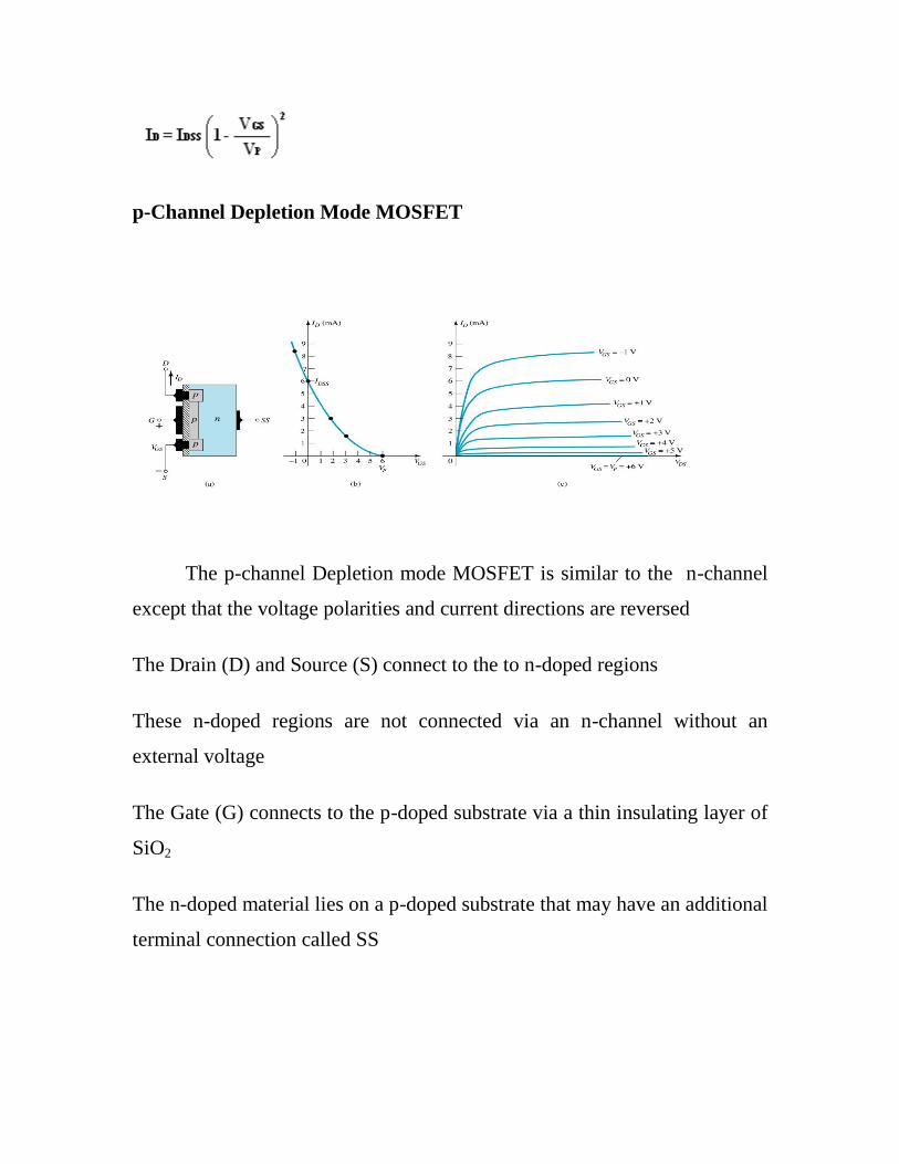
p-Channel Depletion Mode MOSFET
The p-channel Depletion mode MOSFET is similar to the n-channel
except that the voltage polarities and current directions are reversed
The Drain (D) and Source (S) connect to the to n-doped regions
These n-doped regions are not connected via an n-channel without an
external voltage
The Gate (G) connects to the p-doped substrate via a thin insulating layer of
SiO2
The n-doped material lies on a p-doped substrate that may have an additional
terminal connection called SS
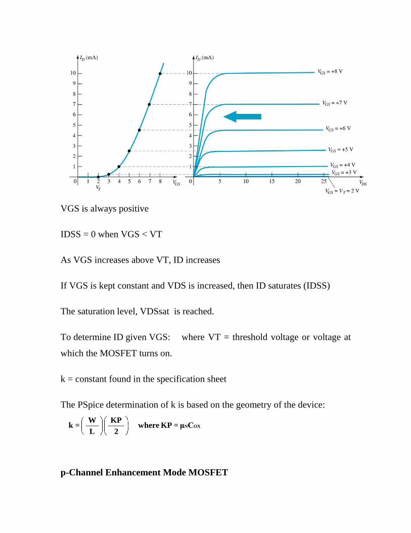
VGS is always positive
IDSS = 0 when VGS < VT
As VGS increases above VT, ID increases
If VGS is kept constant and VDS is increased, then ID saturates (IDSS)
The saturation level, VDSsat is reached.
To determine ID given VGS: where VT = threshold voltage or voltage at
which the MOSFET turns on.
k = constant found in the specification sheet
The PSpice determination of k is based on the geometry of the device:
p-Channel Enhancement Mode MOSFET
N OX W KP
k = where KP = μ C L 2
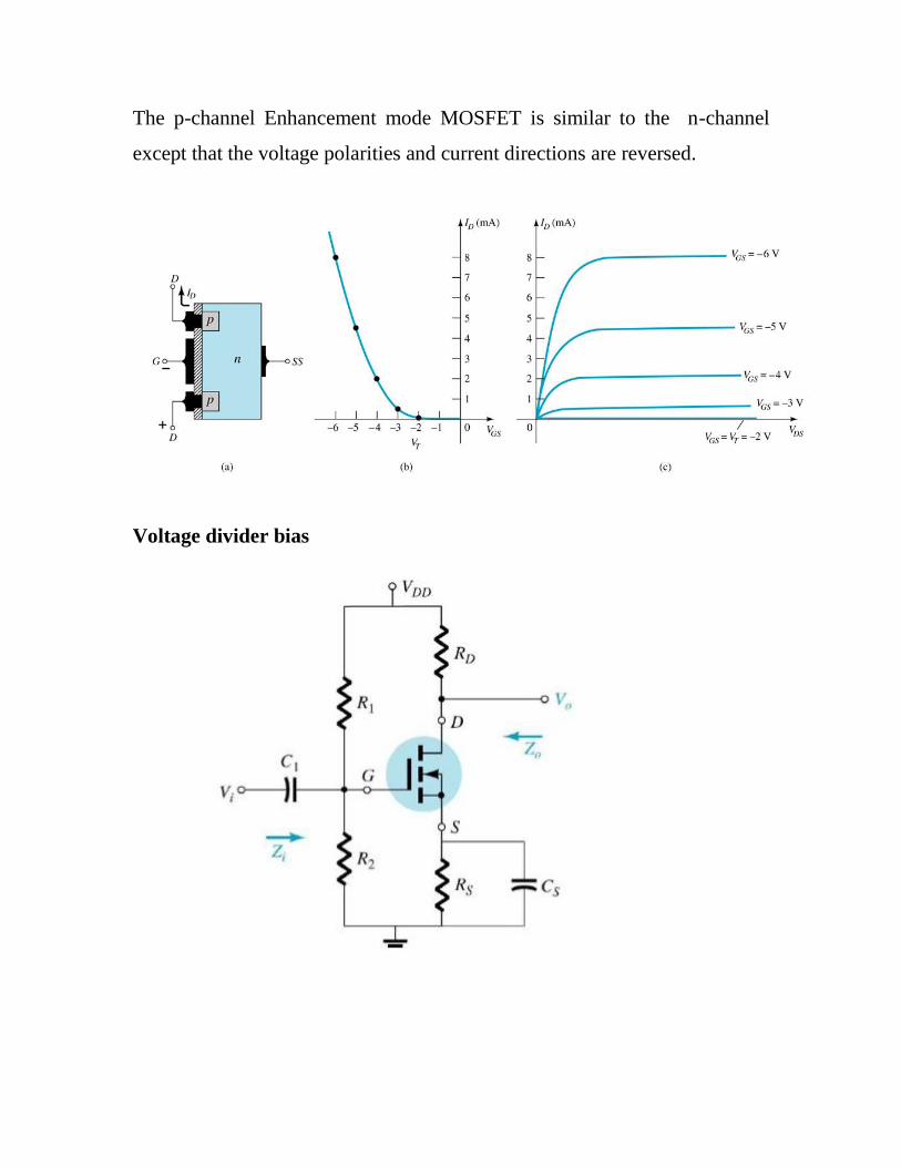
The p-channel Enhancement mode MOSFET is similar to the n-channel
except that the voltage polarities and current directions are reversed.
Voltage divider bias

Drain feedback bias
SCR
The thyristor is a four-layer, three terminal semiconducting device, with
each layer consisting of alternately N-type or P-type material, for example
P-N-P-N. The main terminals, labeled anode and cathode, are across the full
four layers, and the control terminal, called the gate, is attached to p-type
material near to the cathode. (A variant called an SCS—Silicon Controlled
Switch—brings all four layers out to terminals.) The operation of a thyristor
can be understood in terms of a pair of tightly coupled bipolar junction
transistors, arranged to cause the self-latching action:

Thyristors have three states:
1. Reverse blocking mode — Voltage is applied in the direction that
would be blocked by a diode
2. Forward blocking mode — Voltage is applied in the direction
that would cause a diode to conduct, but the thyristor has not yet
been triggered into conduction
3. Forward conducting mode — The thyristor has been triggered
into conduction and will remain conducting until the forward
current drops below a threshold value known as the "holding
current"
Function of the gate terminal
The thyristor has three p-n junctions (serially named J1, J2, J3 from the
anode).

Layer diagram of thyristor.
When the anode is at a positive potential VAK with respect to the cathode
with no voltage applied at the gate, junctions J1 and J3 are forward
biased, while junction J2 is reverse biased. As J2 is reverse biased, no
conduction takes place (Off state). Now if VAK is increased beyond the
breakdown voltage VBO of the thyristor, avalanche breakdown of J2 takes
place and the thyristor starts conducting (On state).
If a positive potential VG is applied at the gate terminal with respect to
the cathode, the breakdown of the junction J2 occurs at a lower value
of VAK. By selecting an appropriate value of VG, the thyristor can be
switched into the on state suddenly.
Once avalanche breakdown has occurred, the thyristor continues to
conduct, irrespective of the gate voltage, until both: (a) the
potential VG is removed and (b) the current through the device
(anode−cathode) is less than the holding current specified by the
manufacturer. Hence VG can be a voltage pulse, such as the voltage
output from a UJT relaxation oscillator.
These gate pulses are characterized in terms of gate trigger voltage (VGT)
and gate trigger current (IGT). Gate trigger current varies inversely with

gate pulse width in such a way that it is evident that there is a minimum
gate charge required to trigger the thyristor.
Switching characteristics
in a conventional thyristor, once it has been switched on by the gate
terminal, the device remains latched in the on-state (i.e. does not need a
continuous supply of gate current to conduct), providing the anode
current has exceeded the latching current (IL). As long as the anode
remains positively biased, it cannot be switched off until the anode
current falls below the holding current (IH).
V - I characteristics.
A thyristor can be switched off if the external circuit causes the anode to
become negatively biased. In some applications this is done by
switching a second thyristor to discharge a capacitor into the cathode of
the first thyristor. This method is called forced commutation.
After a thyristor has been switched off by forced commutation, a finite
time delay must have elapsed before the anode can again be positively
biased and retain the thyristor in the off-state. This minimum delay is
called the circuit commutated turn off time (tQ). Attempting to positively
bias the anode within this time causes the thyristor to be self-triggered

by the remaining charge carriers (holes and electrons) that have not
yet recombined.
For applications with frequencies higher than the domestic AC mains
supply (e.g. 50 Hz or 60 Hz), thyristors with lower values of tQ are
required. Such fast thyristors are made by diffusing into the
silicon heavy metals ions such as gold or platinum which act as charge
combination centres. Alternatively, fast thyristors may be made
by neutron irradiation of the silicon.
The SIDAC is a less common electrically similar device, the difference in
naming being determined by the manufacturer. In general, SIDACs have
higher breakover voltages and current handling.
The SIDAC, or Silicon Diode for Alternating Current, is another member of
the thyristor family. Also referred to as a SYDAC (Silicon thyristor for
Alternating Current), bi-directional thyristor breakover diode, or more
simply a bi-directional thyristor diode, it is technically specified as a
bilateral voltage triggered switch. Its operation is similar to that of the
DIAC, but SIDAC is always a five-layer device with low-voltage drop in
latched conducting state, more like a voltage triggered TRIAC without a
gate. In general, SIDACs have higher breakover voltages and current
handling capacities than DIACs, so they can be directly used for switching
and not just for triggering of another switching device.
The operation of the SIDAC is functionally similar to that of a spark gap.
The SIDAC remains nonconducting until the applied voltage meets or
exceeds its rated breakover voltage. Once entering this conductive state
going through the negative dynamic resistance region, the SIDAC continues
to conduct, regardless of voltage, until the applied current falls below its

rated holding current. At this point, the SIDAC returns to its initial
nonconductive state to begin the cycle once again.
Somewhat uncommon in most electronics, the SIDAC is relegated to the
status of a special purpose device. However, where part-counts are to be
kept low, simple relaxation oscillators are needed, and when the voltages are
too low for practical operation of a spark gap, the SIDAC is an indispensable
component.
Similar devices, though usually not functionally interchangeable with
SIDACs, are the Thyristor Surge Protection Devices (TSPD), Trisil, SID
Actor, or the now-obsolete Surgector. These are designed to tolerate large
surge currents for the suppression of overvoltage transients.
Idealized breakover diode voltage and current relationships. Once the
voltage exceeds the turn-on threshold, the device turns on and the
voltage rapidly falls while the current increases.
Gate Trigger Voltage and Gate Trigger Current: they are the input signal
conditions needed to trigger the TRIAC. We must choose the input voltage
and limiting resistor in order to get a several times higher current than the
required for the triggering. Let's analize just that part of the circuit.

In our example, we want to use
a 12 Volt pulse, but we cannot
apply it directly to the gate, we
need a limiting resistor. We
know that the gate trigger
voltage is 2 Volt as a
maximum. The gate trigger
current is 10mA, so we will
choose a bigger value in order
to assure the triggering, let's
take 30 mA. The voltage
across the resistor is:
So if we want a gate trigger
current of approximately 30
mA, we will need a limiting
resistor of 330 ohm, this way
the gate current is:
(by Ohm's law)
Latching and Holding Current: these parameters refer to the current
between T2 and T1 terminals, which is the same that the load current. As we
said before, once triggered, the TRIAC will remain conducting. Well this is

true whenever the current on the load at the moment of the triggering
exceeds the Latching Current. And when we said "It will switch off when
the current becomes too low", this threshhold is specified by the Holding
Current value, which is lower than the latching current.
From a practical point of view, we just need to verify that the load current is
far bigger than the latching and holding currents (five to ten times at least).
In our case, the latching current is 30mA, so the circuit will work perfectly
with currents above 150mA rms.
Let's assume that we are going to drive a pure resistive load, as a solderer, as
the rms voltage is 110 Volt, the solderer's minimum power should be:
This assures that the TRIAC will be able to conduce near the 100% of the
hemicycle when needed.
In the previous explanations, we have used a pulse to trigger the
TRIAC, and this is an usual practice, but, is it mandatory?
No, it is not, in fact you can switch on the TRIAC with a DC voltage
and keep it active for an indefinite period of time.
The importance of the TRIACs is that they allow us to drive a high
voltage AC load from a low-voltage electronic circuit, as we will see
next.
The basic structure of a unijunction transistor (UJT) is shown in Fig.1. It is
essentially a bar of N type semiconductor material into which P type
material has been diffused somewhere along its length. Contacts are then

made to the device as shown; these are referred to as the emitter, base 1 and
base 2 respectively. Fig.2 shows the schematic symbol used to denote a UJT
in circuit diagrams. For ease of manufacture alternative methods of making
contact with the bar have been developed, giving rise to the two types of
structure - bar and cube - shown in Fig.3
The equivalent circuit shown in Fig.4 has been developed to explain how the
device works, and it is necessary to define the terms used in this explanation.
RBB is known as the interbase resistance, and is the sum of RB1 and RB2:
RBB = RB1 + RB2 (1)
N.B. This is only true when the emitter is open circuit.
VRB1 is the voltage developed across RB1; this is given by the voltage divider
rule:
RB1
VRB1 = (2)
RB1 + RB2
Since the denominator of equation 2 is equal to equation 1, the former can be
rewritten as:
RB1
VRB1 = x VBB (3)
RBB
The ratio RB1 / RBB is referred to as the intrinsic standoff ratio and is denoted
by (the Greek letter eta).
If an external voltage Ve is connected to the emitter, the equivalent circuit
can be redrawn as shown in Fig.5.
If Ve is less than VRB1, the diode is reverse biased and the circuit behaves as
though the emitter was open circuit. If however Ve is increased so that it
exceeds VRB1 by at least 0.7V, the diode becomes forward biased and emitter
current Ie flows into the base 1 region. Because of this, the value of RB1

decreases. It has been suggested that this is due to the presence of additional
charge carriers (holes) in the bar. Further increase in Ve causes the emitter
current to increase which in turn reduces RB1 and this causes a further
increase in current. This runaway effect is termed regeneration. The value of
emitter voltage at which this occurs is known as the peak voltage VP and is
given by: VP = AVVBB + VD (4)
The characteristics of the UJT are illustrated by the graph of emitter voltage
against emitter current (Fig.6).
As the emitter voltage is increased, the current is very small - just a few
microamps. When the peak point is reached, the current rises rapidly, until at

the valley point the device runs into saturation. At this point RB1 is at its
lowest value, which is known as the saturation resistance.
The simplest application of a UJT is as a relaxation oscillator, which is
defined as one in which a capacitor is charged gradually and then discharged
rapidly. The basic circuit is shown in Fig.7; in the practical circuit of Fig.8
R3 limits the emitter current and provides a voltage pulse, while R2 provides
a measure of temperature compensation. Fig. 9 shows the waveforms
occurring at the emitter and base 1; the first is an approximation to a
sawtooth and the second is a pulse of short duration.
The operation of the circuit is as follows: C1 charges through R1 until the
voltage across it reaches the peak point. The emitter current then rises
rapidly, discharging C1 through the base 1 region and R3. The sudden rise of
current through R3 produces the voltage pulse. When the current falls to IV
the UJT switches off and the cycle is repeated.
It can be shown that the time t between successive pulses is given by:

VBB - VV
t + R1C ln secs (5) N.B. R measured in Megaohms. C in µF.
VBB - VP
Question Bank
PART –A
1.Define pinch-off voltage.
2. What is intrinsic stand-off ratio of UJT?
PART-B
1.(a) describe the different manufacturing techniques adopted to reduce the magnitude of
gate source threshold voltage Vj in enhancement MOSFET.
(b) Compare the performance of JFET with MOSFET.
(c) Discuss the relative performance of p-channel MOSFET and n-channel MOSFET.
2.(a) Explain the working and characteristics of DIAC.
(b) Write short notes on MOSFET biasing.
UNIT III AMPLIFIERS
CE, CC and CB amplifiers – Small-signal low frequency transistor amplifier circuits –h-
parameter representation of a transistor – Analysis of single stage transistor amplifier
circuits – Voltage gain – Current gain – Input impedance and output impedance –
Frequency response – RC coupled amplifier – Classification of Power amplifiers – Class
A, B, AB and C Power amplifiers – Push-Pull and Complementary-Symmetry amplifiers
– Design of power output, efficiency and cross-over distortion.

UNIT III
AMPLIFIERS
CE, CC and CB amplifiers
Small-signal models
hybrid-pi model
h-parameter model
Another model commonly used to analyze BJT circuits is the "h-
parameter" model, closely related to the hybrid-pi model and the y-
parameter two-port, but using input current and output voltage as
independent variables, rather than input and output voltages. This two-port
network is particularly suited to BJTs as it lends itself easily to the analysis
of circuit behaviour, and may be used to develop further accurate models. As
shown, the term "x" in the model represents a different BJT lead depending
on the topology used. For common-emitter mode the various symbols take
on the specific values as:
x = 'e' because it is a common-emitter topology

Terminal 1 = Base
Terminal 2 = Collector
Terminal 3 = Emitter
ii = Base current (ib)
io = Collector current (ic)
Vin = Base-to-emitter voltage (VBE)
Vo = Collector-to-emitter voltage (VCE)
and the h-parameters are given by:
hix = hie – The input impedance of the transistor (corresponding to the
emitter resistance re).
hrx = hre – Represents the dependence of the transistor's IB–VBE curve
on the value of VCE. It is usually very small and is often neglected
(assumed to be zero).
hfx = hfe – The current-gain of the transistor. This parameter is often
specified as hFE or the DC current-gain (βDC) in datasheets.
hox = hoe – The output impedance of transistor. This term is usually
specified as an admittance and has to be inverted to convert it to an
impedance.
As shown, the h-parameters have lower-case subscripts and hence signify
AC conditions or analyses. For DC conditions they are specified in upper-
case. For the CE topology, an approximate h-parameter model is commonly
used which further simplifies the circuit analysis. For this
the hoe and hre parameters are neglected (that is, they are set to infinity and
zero, respectively). It should also be noted that the h-parameter model as
shown is suited to low-frequency, small-signal analysis. For high-frequency

analyses the inter-electrode capacitances that are important at high
frequencies must be added.
Applications
The BJT remains a device that excels in some applications, such as discrete
circuit design, due to the very wide selection of BJT types available, and
because of its high transconductance and output resistance compared
to MOSFETs. The BJT is also the choice for demanding analog circuits,
especially for very-high-frequency applications, such as radio-
frequency circuits for wireless systems. Bipolar transistors can be combined
with MOSFETs in an integrated circuit by using a BiCMOS process of
wafer fabrication to create circuits that take advantage of the application
strengths of both types of transistor.
Temperature sensors
Because of the known temperature and current dependence of the forward-
biased base–emitter junction voltage, the BJT can be used to measure
temperature by subtracting two voltages at two different bias currents in a
known ratio [3].
Logarithmic converters
Because base–emitter voltage varies as the log of the base–emitter and
collector–emitter currents, a BJT can also be used to
compute logarithms and anti-logarithms. A diode can also perform these
nonlinear functions, but the transistor provides more circuit flexibility.
Common base

it is usually employed for amplifiers that require an unusually low input
impedance, for example to act as a preamplifier for moving-
coil microphones. However, it is popular in high-frequency amplifiers, for
example for VHF and UHF, because its input capacitance does not suffer
from the Miller effect, which degrades the bandwidth of the common-
emitter configuration, and because of the relatively high isolation between
the input and output. This high isolation means that there is little feedback
from the output back to the input, leading to high stability.
This configuration is also useful as a current buffer since it has a current
gain of approximately unity (see formulas below). Often a common base is
used in this manner, preceded by a common-emitter stage. The combination
of these two form the cascode configuration, which possesses several of the
benefits of each configuration, such as high input impedance and isolation.
Low frequency characteristics
At low frequencies and under small-signal conditions, the circuit in Figure 1
can be represented by that in Figure 2, where the hybrid-pi model for the
BJT has been employed. The input signal is represented by
a Thévenin voltage source, vs, with a series resistance Rs and the load is a
resistor RL. This circuit can be used to derive the following characteristics of
the common-base amplifier.
Definitio
n Expression
Approximate
expression Conditions

Open-
circuit v
oltage
gain
Short-
circuit c
urrent
gain
1
Input
resistan
ce
Output
resistan
ce
RC | | rO
Note: Parallel lines (||) indicate components in parallel.
In general the overall voltage/current gain may be substantially less than the
open/short circuit gains listed above (depending on the source and load
resistances) due to the loading effect.
Active loads

For voltage amplification, the range of allowed output voltage swing in this
amplifier is tied to its voltage gain when a resistor load RC is employed, as in
Figure 1. That is, large voltage gain requires largeRC, and that in turn implies
a large DC voltage drop across RC. For a given supply voltage, the larger this
drop, the smaller the transistor VCB and the less output swing is allowed
before saturation of the transistor occurs, with resultant distortion of the
output signal. To avoid this situation, an active load can be used, for
example, a current mirror. If this choice is made, the value of RC in the table
above is replaced by the small-signal output resistance of the active load,
which is generally at least as large as the rO of the active transistor in Figure
1. On the other hand, the DC voltage drop across the active load is a fixed
low value (the compliance voltage of the active load), much less than the
DC voltage drop incurred for comparable gain using a resistor RC. That is, an
active load imposes less restriction on the output voltage swing. Notice that
active load or not, large AC gain still is coupled to large AC output
resistance, which leads to poor voltage division at the output except for large
loads RL >> Rout.
For use as a current buffer, gain is not affected by RC, but output resistance
is. Because of the current division at the output, it is desirable to have an
output resistance for the buffer much larger than the load RL being driven so
large signal currents can be delivered to a load. If a resistor RC is used, as in
Figure 1, a large output resistance is coupled to a large RC, again limiting the
signal swing at the output. (Even though current is delivered to the load,
usually a large current signal into the load implies a large voltage swing
across the load as well.) An active load provides high AC output resistance
with much less serious impact upon the amplitude of output signal swing.

Voltage amplifier
Small-signal model for calculating various parameters; Thévenin
voltage source as signal.
For the case when the common-base circuit is used as a voltage amplifier,
the circuit is shown in Figure
The output resistance is large, at least RC || rO, the value which arises with
low source impedance (RS << rE). A large output resistance is undesirable in
a voltage amplifier, as it leads to poor voltage division at the output.
Nonetheless, the voltage gain is appreciable even for small loads: according
to the table, with RS = rE the gain is Av = gm RL / 2. For larger source
impedances, the gain is determined by the resistor ratioRL / RS, and not by
the transistor properties, which can be an advantage where insensitivity to
temperature or transistor variations is important.
An alternative to the use of the hybrid-pi model for these calculations is a
general technique based upon two-port networks. For example, in an
application like this one where voltage is the output, a g-equivalent two-port
could be selected for simplicity, as it uses a voltage amplifier in the output
port.

For RS values in the vicinity of rE the amplifier is transitional between
voltage amplifier and current buffer. For RS >> rE the driver representation
as a Thévenin source should be replaced by representation with a Norton
source. The common-base circuit stops behaving like a voltage amplifier and
behaves like a current follower, as discussed next.
Common-base circuit with Norton driver; RC is omitted because an active
load is assumed with infinite small-signal output resistance
Figure shows the common-base amplifier used as a current follower. The
circuit signal is provided by an AC Norton source (current IS, Norton
resistance RS) at the input, and the circuit has a resistor load RL at the output.
As mentioned earlier, this amplifier is bilateral as a consequence of the
output resistance rO, which connects the output to the input. In this case the
output resistance is large even in the worst case (it is at least rO || RC and can
become (β + 1) rO || RC for large RS). Large output resistance is a desirable
attribute of a current source because favorable current division sends most of
the current to the load. The current gain is very nearly unity as long as RS >>
rE.

An alternative analysis technique is based upon two-port networks. For example, in an
application like this one where current is the output, an h-equivalent two-port is selected
because it uses a current amplifier in the output port.
A common-collector amplifier (also known as an emitter follower or BJT voltage
follower) is one of three basic single-stage bipolar junction transistor (BJT)
amplifier topologies, typically used as a voltage buffer. In this circuit the base
terminal of the transistor serves as the input, the emitter the output, and the
collector is common to both (for example, it may be tied to ground reference or
a power supply rail), hence its name. The analogous field-effect transistor circuit is
the common-drain amplifier.
Figure 1: Basic NPN common-collector circuit
(neglecting biasing details).
Basic circuit

The circuit can be explained by viewing the transistor as being under the
control of negative feedback. From this viewpoint, a common-collector stage
(Fig. 1) is an amplifier with full series negative feedback. In this
configuration (Fig. 2 with β = 1), the entire output voltage VOUT is placed
contrary and in series with the input voltage VIN. Thus the two voltages are
subtracted according to KVL (the subtractor from the function block
diagram is implemented just by the input loop) and their difference Vdiff =
VIN - VOUT is applied to the base-emitter junction. The transistor monitors
continuously Vdiff and adjusts its emitter voltage almost equal (less VBEO) to
the input voltage by passing the according collector current through the
emitter resistor RE. As a result, the output voltage follows the input voltage
variations from VBEO up to V+; hence the name, emitter follower. Intuitively,
this behavior can be also understood by realizing that the base-emitter
voltage in the bipolar transistor is very insensitive to bias changes, so any
change in base voltage is transmitted (to good approximation) directly to the
emitter. It depends slightly on various disturbances (transistor tolerances,
temperature variations, load resistance, collector resistor if it is added, etc.)
since the transistor reacts to these disturbances and restores the equilibrium.
It never saturates even if the input voltage reaches the positive rail.
The common collector circuit can be shown mathematically to have
a voltage gain of almost unity:

: PNP version of the emitter follower circuit, all
polarities are reversed.
A small voltage change on the input terminal will be replicated at the
output (depending slightly on the transistor's gain and the value of
the load resistance; see gain formula below). This circuit is useful
because it has a large input impedance, so it will not load down the
previous circuit:
and a small output impedance, so it can drive low-resistance loads:
Typically, the emitter resistor is significantly larger and can be removed
from the equation:
One aspect of buffer action is transformation of impedances. For example,
the Thévenin resistance of a combination of a voltage follower driven by a
voltage
Application

NPN voltage follower withcurrent source biasing suitable for integrated
circuits
The low output impedance allows a source with a large output impedance to
drive a small load impedance; it functions as a voltage buffer. In other
words, the circuit has current gain (which depends largely on the hFE of the
transistor) instead of voltage gain. A small change to the input current results
in much larger change in the output current supplied to the output load.
One aspect of buffer action is transformation of impedances. For example,
the Thévenin resistance of a combination of a voltage follower driven by a
voltage source with high Thevenin resistance is reduced to only the output
resistance of the voltage follower, a small resistance. That resistance
reduction makes the combination a more ideal voltage source. Conversely, a
voltage follower inserted between a small load resistance and a driving stage
presents a large load to the driving stage, an advantage in coupling a voltage
signal to a small load.
This configuration is commonly used in the output stages of class-
B and class-ABamplifier — the base circuit is modified to operate the
transistor in class-B or AB mode. In class-A mode, sometimes an

active current source is used instead of RE (Fig. 4) to improve linearity
and/or efficiency.[1]
Characteristics
At low frequencies and using a simplified hybrid-pi model, the
following small-signal characteristics can be derived. (Parameter β
= gmrπ and the parallel lines indicate components in parallel.)
Definitio
n Expression
Approximat
e expression Conditions
Current g
ain
Voltage g
ain
Input
resistance
Output
resistance
Where is the Thévenin equivalent source resistance.
Derivations
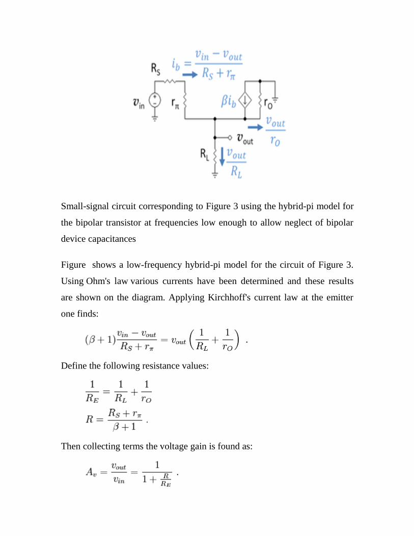
Small-signal circuit corresponding to Figure 3 using the hybrid-pi model for
the bipolar transistor at frequencies low enough to allow neglect of bipolar
device capacitances
Figure shows a low-frequency hybrid-pi model for the circuit of Figure 3.
Using Ohm's law various currents have been determined and these results
are shown on the diagram. Applying Kirchhoff's current law at the emitter
one finds:
Define the following resistance values:
Then collecting terms the voltage gain is found as:

From this result the gain approaches unity (as expected for a buffer
amplifier) if the resistance ratio in the denominator is small. This ratio
decreases with larger values of current gain β and with larger vales of RE.
The input resistance is found as:
The transistor output resistance rO ordinarily is large compared to the
load RL and therefore RL dominates RE. From this result, the input resistance
of the amplifier is much larger than the output load resistance RL for large
current gain β. That is, placing the amplifier between the load and the source
presents a smaller (high-resistive) load to the source than direct coupling
to RL, which results in less signal attenuation in the source impedance RS as a
consequence of voltage division
Low-frequency small-signal circuit for bipolar voltage follower with test
current at output for finding output resistance. Resistor RE = RL | |rO.

Figure shows the small-signal circuit of Figure 5 with the input short-
circuited and a test current placed at its output. The output resistance is
found using this circuit as:
Using Ohm's law, various currents have been found, as indicated on the
diagram. Collecting the terms for the base current, the base current is found
as:
where RE is defined above. Using this value for base current, Ohm's law
provides vx as:
Substituting for the base current, and collecting terms,
where || denotes a parallel connection and R is defined above.
Because R generally is a small resistance when the current gain β is
large, R dominates the output impedance which therefore also is small. A
small output impedance means the series combination of the original voltage
source and the voltage follower presents a Thévenin voltage source with a
lower Thévenin resistance at its output node; that is, the combination of
voltage source with voltage follower makes a more ideal voltage source than
the original one.
Single stage amplifier
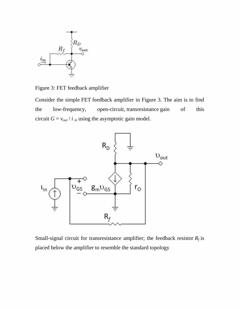
Figure 3: FET feedback amplifier
Consider the simple FET feedback amplifier in Figure 3. The aim is to find
the low-frequency, open-circuit, transresistance gain of this
circuit G = vout / i in using the asymptotic gain model.
Small-signal circuit for transresistance amplifier; the feedback resistor Rf is
placed below the amplifier to resemble the standard topology

Small-signal circuit with return path broken and test voltage driving
amplifier at the break
The small-signal equivalent circuit is shown in Figure 4, where the transistor
is replaced by its hybrid-pi model.
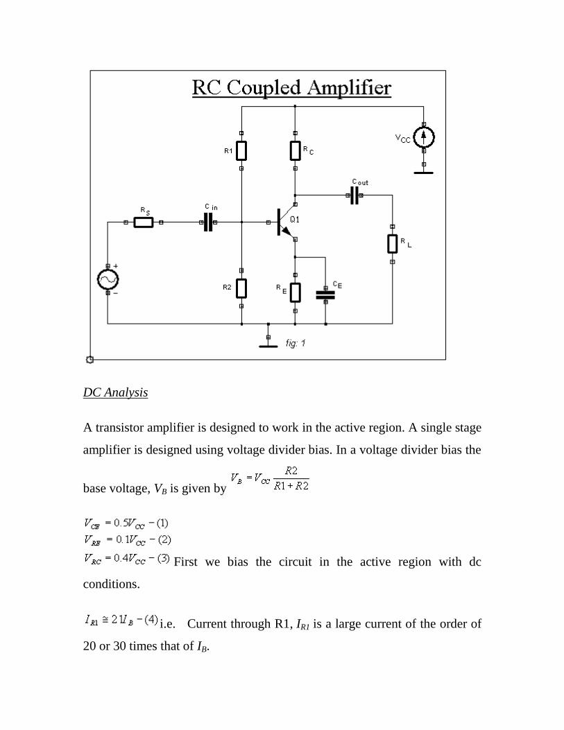
DC Analysis
A transistor amplifier is designed to work in the active region. A single stage
amplifier is designed using voltage divider bias. In a voltage divider bias the
base voltage, VB is given by
First we bias the circuit in the active region with dc
conditions.
i.e. Current through R1, IR1 is a large current of the order of
20 or 30 times that of IB.

Current through R2, IR2 is given by
AC Analysis
Modifications required from the dc circuit are
1. Coupling capacitors (Cin, Cout)
2. Bypass Capacitor CE.
The function of the coupling capacitor is to isolate the amplifier input circuit
from the source. Since capacitor blocks dc it does not allow the dc

components from the input circuit to get to the base of transistor and to
change the Q point.
Additional requirement if Cin is that it must pass the input ac signal
unattenuated. Hence the lower cut-off frequency (LCF) of the amplifier is
determined by the coupling capacitor. The coupling capacitor Cin along with
resistance combinations shown in fig forms a high pass filter whose cut-off
frequency; .
The LCF due to Cin;
At mid or high frequencies capacitor almost acts as a short circuit.
Then Vi is related to VS by;

Effect of Cout
The effect of Cout on LCF is given by;
where .
Effect of CE
CE is designed such that impedance of the capacitor must be less than
of RE across which it is connected at LCF. The function of CE is to bypass
the emitter resistor during ac operation other wise during amplification with
increase or decrease in current, the drop across RE will increase or decrease
and hence VBE decreases or increases opposing the change in current. So the
function of RE is limited to dc where the capacitor will be open and RE will
stabilize the circuit. In the case of ac the capacitor will take over current.
Power amplifier classes
Angle of flow or conduction angle
Power amplifier circuits (output stages) are classified as A, B, AB and C for
analog designs, and class D and E for switching designs based upon the
conduction angle or angle of flow, Θ, of the input signal through the (or
each) output amplifying device, that is, the portion of the input signal cycle
during which the amplifying device conducts. The image of the conduction
angle is derived from amplifying a sinusoidal signal. (If the device is always
on, Θ = 360°.) The angle of flow is closely related to the amplifier power
efficiency. The various classes are introduced below, followed by more
detailed discussion under individual headings later on.
Class A
100% of the input signal is used (conduction angle Θ = 360° or 2π);
i.e., the active element remains conducting[5]
(works in its "linear"
range) all of the time. Where efficiency is not a consideration, most
small signal linear amplifiers are designed as Class A. Class A
amplifiers are typically more linear and less complex than other types,
but are very inefficient. This type of amplifier is most commonly used
in small-signal stages or for low-power applications (such as driving
headphones). Subclass A2 is sometimes used to refer to vacuum tube
Class A stages where the grid is allowed to be driven slightly positive
on signal peaks, resulting in slightly more power than normal Class A
(A1; where the grid is always negative[6]
), but incurring more
distortion.
Class B

50% of the input signal is used (Θ = 180° or π; i.e., the active element
works in its linear range half of the time and is more or less turned off
for the other half). In most Class B, there are two output devices (or
sets of output devices), each of which conducts alternately (push–pull)
for exactly 180° (or half cycle) of the input signal; selective RF
amplifiers can also be implemented using a single active element.
These amplifiers are subject to crossover distortion if the transition
from one active element to the other is not perfect, as when two
complementary transistors (i.e., one PNP, one NPN) are connected as
two emitter followers with their base and emitter terminals in
common, requiring the base voltage to slew across the region where
both devices are turned off.[7]
Class AB
Here the two active elements conduct more than half of the time as a
means to reduce the cross-over distortions of Class B amplifiers. In
the example of the complementary emitter followers a bias network
allows for more or less quiescent current thus providing an operating
point somewhere between Class A and Class B. Sometimes a figure is
added (e.g., AB1 or AB2) for vacuum tube stages where the grid
voltage is always negative with respect to the cathode (Class AB1) or
may be slightly positive (hence drawing grid current, adding more
distortion, but giving slightly higher output power) on signal peaks
(Class AB2); another interpretation being higher figures implying a
higher quiescent current and therefore more of the properties of Class
A.
Class C

Less than 50% of the input signal is used (conduction angle Θ <
180°). The advantage is potentially high efficiency, but a disadvantage
is high distortion.
Class D
Main article: Switching amplifier
These use switching to achieve a very high power efficiency (more
than 90% in modern designs). By allowing each output device to be
either fully on or off, losses are minimized. The analog output is
created by pulse-width modulation; i.e., the active element is switched
on for shorter or longer intervals instead of modifying its resistance.
There are more complicated switching schemes like sigma-delta
modulation, to improve some performance aspects like lower
distortions or better efficiency.
Additional classes
There are several other amplifier classes, although they are mainly
variations of the previous classes. For example, Class G and Class H
amplifiers are marked by variation of the supply rails (in discrete steps
or in a continuous fashion, respectively) following the input signal.
Wasted heat on the output devices can be reduced as excess voltage is
kept to a minimum. The amplifier that is fed with these rails itself can
be of any class. These kinds of amplifiers are more complex, and are
mainly used for specialized applications, such as very high-power
units. Also, Class E and Class F amplifiers are commonly described in
literature for radio frequencies applications where efficiency of the
traditional classes in are important, yet several aspects not covered
elsewhere (e.g.: amplifiers often simply said to have a gain of x dB -
so what power gain?) deviate substantially from their ideal values.

These classes use harmonic tuning of their output networks to achieve
higher efficiency and can be considered a subset of Class C due to
their conduction angle characteristics.
The classes can be most easily understood using the diagrams in each
section below. For the sake of illustration, a bipolar junction transistor is
shown as the amplifying device, but in practice this could be a MOSFET or
vacuum tube device. In an analog amplifier (the most common kind), the
signal is applied to the input terminal of the device (base, gate or grid), and
this causes a proportional output drive current to flow out of the output
terminal. The output drive current comes from the power supply.
Class A
Class A amplifier
Amplifying devices operating in Class A conduct over the whole of the input
cycle such that the output signal is an exact scaled-up replica of the input
with no clipping. A Class A amplifier (or operational amplifier) is
distinguished by the output stage (and perhaps the driver) device(s) being
biased into Class A; even Class AB and B amplifiers normally have early
stages operating in Class A. Class A is the usual means of implementing
small-signal amplifiers, so the term Class A design applied to equipment

such as preamplifiers (for example, in recording studios) implies not so
much their use of Class A, but that their sound is top quality - good enough
to be matched with top quality Class A power amplifiers.
Advantages of Class A Amplifiers
Class A designs are simpler than other classes; for example Class AB
and B designs require two devices (push-pull output) to handle both
halves of the waveform, and circuitry to keep the quiescent bias
optimal during temperature changes; Class A can use either single-
ended or push-pull and bias is usually less critical.
The amplifying element is biased so the device is always conducting
to some extent, normally implying the quiescent (small-signal)
collector current (for transistors; drain current for FETs or anode/plate
current for vacuum tubes) is close to the most linear portion
(sometimes called the "sweet spot") of its characteristic curve (known
as its transfer characteristic or transconductance curve), giving the
least audio distortion.
Because the device is never shut off completely there is no "turn on"
time, little problem with charge storage, and generally better high
frequency performance and feedback loop stability (and usually fewer
high-order harmonics).
The point at which the device comes closest to being cut off (and so
significant change in gain, hence non-linearity) is not close to zero
signal, so the problem of crossover distortion associated with Class
AB and B designs is avoided, even in Class A double-ended stages.

Disadvantage of Class A Amplifiers
They are very inefficient; a theoretical maximum of 50% is obtainable
with inductive output coupling and only 25% with capacitive
coupling, unless Square law output stages are used. In a power
amplifier this not only wastes power and limits battery operation, it
may place restrictions on the output devices that can be used (for
example: ruling out some audio triodes if modern low-efficiency
loudspeakers are to be used), and will increase costs. Inefficiency
comes not just from the fact that the device is always conducting to
some extent (that happens even with Class AB, yet its efficiency can
be close to that of Class B); it is that the standing current is roughly
half the maximum output current (although this can be less with
Square law output stage), together with the problem that a large part
of the power supply voltage is developed across the output device at
low signal levels (as with Classes AB and B, but unlike output stages
such as Class D). If high output powers are needed from a Class A
circuit, the power waste (and the accompanying heat) will become
significant. For every watt delivered to the load, the amplifier itself
will, at best, dissipate another watt. For large powers this means very
large and expensive power supplies and heat sinking.
Class A designs have largely been superseded by the more efficient designs
for power amplifiers, though they remain popular with some hobbyists,
mostly for their simplicity. Also, many audiophiles believe that Class A
gives the best sound quality (for their absence of crossover distortion and
reduced odd-harmonic and high-order harmonic distortion) which provides a
small market for expensive high fidelity Class A amps.
Single-Ended and Triode Class A Amplifiers
Some aficionados who prefer Class A amplifiers also prefer the use of
thermionic valve (or "tube") designs instead of transistors, especially in
Single-ended triode output configurations for several claimed reasons:
Single-ended output stages (be they tube or transistor) have an
asymmetrical transfer function, meaning that even harmonics in the
created distortion tend not to be canceled (as they are in push-pull
output stages); by using tubes OR FETs most of the distortion is from
the square law transfer characteristic and so second-order, which some
consider to be "warmer" and more pleasant.[8][9]
For those who prefer low distortion figures, the use of tubes with
Class A (generating little odd-harmonic distortion, as mentioned
above) together with symmetrical circuits (such as push-pull output
stages, or balanced low-level stages) results in the cancellation of
most of the even distortion harmonics, hence the removal of most of
the distortion.
Though good amplifier design can reduce harmonic distortion patterns
to almost nothing, distortion is essential to the sound of electric guitar
amplifiers, for example, and is held by recording engineers to offer
more flattering microphones and to enhance "clinical-sounding"
digital technology.
Historically, valve amplifiers often used a Class A power amplifier
simply because valves are large and expensive; many Class A designs
use only a single device.

Transistors are much cheaper, and so more elaborate designs that give
greater efficiency but use more parts are still cost-effective. A classic
application for a pair of class A devices is the long-tailed pair, which is
exceptionally linear, and forms the basis of many more complex circuits,
including many audio amplifiers and almost all op-amps. Class A amplifiers
are often used in output stages of high quality op-amps (although the
accuracy of the bias in low cost op-amps such as the 741 may result in Class
A or Class AB or Class B, varying from device to device or with
temperature). They are sometimes used as medium-power, low-efficiency,
and high-cost audio amplifiers. The power consumption is unrelated to the
output power. At idle (no input), the power consumption is essentially the
same as at high output volume. The result is low efficiency and high heat
dissipation.
Class B and AB
Class B amplifiers only amplify half of the input wave cycle, thus creating a
large amount of distortion, but their efficiency is greatly improved and is
much better than Class A. Class B has a maximum theoretical efficiency of
78.5% (i.e., π/4). This is because the amplifying element is switched off
altogether half of the time, and so cannot dissipate power. A single Class B
element is rarely found in practice, though it has been used for driving the
loudspeaker in the early IBM Personal Computers with beeps, and it can be
used in RF power amplifier where the distortion levels are less important.
However Class C is more commonly used for this.

Class B Amplifier
A practical circuit using Class B elements is the push-pull stage, such as the
very simplified complementary pair arrangement shown below. Here,
complementary or quasi-complementary devices are each used for
amplifying the opposite halves of the input signal, which is then recombined
at the output. This arrangement gives excellent efficiency, but can suffer
from the drawback that there is a small mismatch in the cross-over region -
at the "joins" between the two halves of the signal, as one output device has
to take over supplying power exactly as the other finishes. This is called
crossover distortion. An improvement is to bias the devices so they are not
completely off when they're not in use. This approach is called Class AB
operation.
In Class AB operation, each device operates the same way as in Class B over
half the waveform, but also conducts a small amount on the other half. As a
result, the region where both devices simultaneously are nearly off (the
"dead zone") is reduced. The result is that when the waveforms from the two
devices are combined, the crossover is greatly minimized or eliminated
altogether. The exact choice of quiescent current, the standing current
through both devices when there is no signal, makes a large difference to the
level of distortion (and to the risk of thermal runaway, that may damage the

devices); often the bias voltage applied to set this quiescent current has to be
adjusted with the temperature of the output transistors (for example in the
circuit at the beginning of the article the diodes would be mounted
physically close to the output transistors, and chosen to have a matched
temperature coefficient). Another approach (often used as well as thermally-
tracking bias voltages) is to include small value resistors in series with the
emitters.
Push-Pull and Complementary-Symmetry amplifiers
Class AB sacrifices some efficiency over class B in favor of linearity, thus is
less efficient (below 78.5% for full-amplitude sinewaves in transistor
amplifiers, typically; much less is common in Class AB vacuum tube
amplifiers). It is typically much more efficient than class A.
Class B push–pull amplifier
Class B or AB push–pull circuits are the most common design type found in
audio power amplifiers. Class AB is widely considered a good compromise
for audio amplifiers, since much of the time the music is quiet enough that

the signal stays in the "class A" region, where it is amplified with good
fidelity, and by definition if passing out of this region, is large enough that
the distortion products typical of class B are relatively small. The crossover
distortion can be reduced further by using negative feedback. Class B and
AB amplifiers are sometimes used for RF linear amplifiers as well. Class B
amplifiers are also favored in battery-operated devices, such as transistor
radios.
Digital Class B
A limited power output Class-B amplifier with a single-ended supply rail of
5±0.5 V.
Class C
Class C amplifier
Class C amplifiers conduct less than 50% of the input signal and the
distortion at the output is high, but high efficiencies (up to 90%) are
possible. Some applications (for example, megaphones) can tolerate the
distortion. A much more common application for Class C amplifiers is in RF
transmitters, where the distortion can be vastly reduced by using tuned loads
on the amplifier stage. The input signal is used to roughly switch the
amplifying device on and off, which causes pulses of current to flow through
a tuned circuit.
The Class C amplifier has two modes of operation: tuned and untuned.[10]
The diagram shows a waveform from a simple class C circuit without the
tuned load. This is called untuned operation, and the analysis of the
waveforms shows the massive distortion that appears in the signal. When the
proper load (e.g., a pure inductive-capacitive filter) is used, two things
happen. The first is that the output's bias level is clamped, so that the output
variation is centered at one-half of the supply voltage. This is why tuned
operation is sometimes called a clamper. This action of elevating bias level
allows the waveform to be restored to its proper shape, allowing a complete
waveform to be re-established despite having only a one-polarity supply.
This is directly related to the second phenomenon: the waveform on the
center frequency becomes much less distorted. The distortion that is present
is dependent upon the bandwidth of the tuned load, with the center
frequency seeing very little distortion, but greater attenuation the farther
from the tuned frequency that the signal gets.
The tuned circuit will only resonate at particular frequencies, and so the
unwanted frequencies are dramatically suppressed, and the wanted full
signal (sine wave) will be extracted by the tuned load (e.g., a high-quality
bell will ring at a particular frequency when it is hit periodically with a
hammer). Provided the transmitter is not required to operate over a very
wide band of frequencies, this arrangement works extremely well. Other
residual harmonics can be removed using a filter.
Class D

Class D Amplifier
Boss Audio Class D mono car audio amplifier with a low pass filter for
powering subwoofers
In the Class D amplifier the input signal is converted to a sequence of higher
voltage output pulses. The averaged-over-time power values of these pulses
are directly proportional to the instantaneous amplitude of the input signal.
The frequency of the output pulses is typically ten or more times the highest
frequency in the input signal to be amplified. The output pulses contain
inaccurate spectral components (that is, the pulse frequency and its
harmonics) which must be removed by a low-pass passive filter. The
resulting filtered signal is then an amplified replica of the input.
These amplifiers use pulse width modulation, pulse density modulation
(sometimes referred to as pulse frequency modulation) or more advanced
form of modulation such as Delta-sigma modulation (for example, in the
Analog Devices AD1990 Class-D audio power amplifier). Output stages
such as those used in pulse generators are examples of Class D amplifiers.
The term Class D is usually applied to devices intended to reproduce signals
with a bandwidth well below the switching frequency.
Class D amplifiers can be controlled by either analog or digital circuits. The
digital control introduces additional distortion called quantization error
caused by its conversion of the input signal to a digital value.
The main advantage of a Class D amplifier is power efficiency. Because the
output pulses have a fixed amplitude, the switching elements (usually
MOSFETs, but valves and bipolar transistors were once used) are switched
either completely on or completely off, rather than operated in linear mode.
A MOSFET operates with the lowest resistance when fully-on and thus has
the lowest power dissipation when in that condition, except when fully off.
When operated in a linear mode the MOSFET has variable amounts of
resistance that vary linearly with the input voltage and the resistance is
something other than the minimum possible, therefore more electrical
energy is dissipated as heat. Compared to Class A/B operation, Class D's
lower losses permit the use of a smaller heat sink for the MOSFETS while
also reducing the amount of AC power supply power required. Thus, Class
D amplifiers do not need as large or as heavy power supply transformers or
heatsinks, so they are smaller and more compact in size than an equivalent
Class AB amplifier.
Class D amplifiers have been widely used to control motors, and almost
exclusively for small DC motors, but they are now also used as audio
amplifiers, with some extra circuitry to allow analogue to be converted to a
much higher frequency pulse width modulated signal. The relative difficulty
of achieving good audio quality means that nearly all are used in

applications where quality is not a factor, such as modestly-priced bookshelf
audio systems and "DVD-receivers" in mid-price home theater systems.
High quality Class D audio amplifiers are now, however, starting to appear
in the market:
Tripath have called their revised Class D designs Class T.
Bang and Olufsen's ICEPower Class D system has been used in the
Alpine PDX range and some of Pioneer's PRS range and for other
manufacturers' equipment.
These revised designs have been said to rival good traditional AB amplifiers
in terms of quality.
Before these higher quality designs existed an earlier use of Class D
amplifiers and prolific area of application was high-powered, subwoofer
amplifiers in cars. Because subwoofers are generally limited to a bandwidth
of no higher than 150 Hz, the switching speed for the amplifier does not
have to be as high as for a full range amplifier. The drawback with Class D
designs being used to power subwoofers is that their output filters (typically
inductors that convert the pulse width signal back into an analogue
waveform) lower the damping factor of the amplifier.
This means that the amplifier cannot prevent the subwoofer's reactive nature
from lessening the impact of low bass sounds (as explained in the feedback
part of the Class AB section). Class D amplifiers for driving subwoofers are
relatively inexpensive, in comparison to Class AB amplifiers. A 1000 W
Class D subwoofer amplifier that can operate at about 80% to 95%

efficiency costs about US$250, much less than a Class AB amplifier of this
power, which would cost several thousand dollars.
The letter D used to designate this amplifier class is simply the next letter
after C, and does not stand for digital. Class D and Class E amplifiers are
sometimes mistakenly described as "digital" because the output waveform
superficially resembles a pulse-train of digital symbols, but a Class D
amplifier merely converts an input waveform into a continuously pulse-
width modulated (square wave) analog signal. (A digital waveform would be
pulse-code modulated.)
POWER OUTPUT CIRCUITS
PUSH-PULL AMPLIFIERS
VBB determines whether the stage will operate in Class-A, B, AB, or C .
Typically all audio amplifiers are biased to operate in Class-AB in order to
minimize the effects of cross-over distortion at low drive levels and to
benefit from the high efficiency of Class-B operation at medium and high
volume. In this push-pull amplifier, QA will turn on and amplify when vIN is
positive; QB will turn on and amplify when vIN is negative. The center-

tapped transformer, T1 makes sure the transistors get the right polarity to
turn on (both require positive voltage on their bases to turn on) but receive
alternate halves of vIN . The center-tapped transformer, T2 superimposes the
amplified halves by combining them with opposite phases, thereby
correcting for the phase reversal introduced by T1. RL receives the amplified
halves superimposed with the correct polarity for each, therefore the whole
waveform is reproduced on it at amplified levels. Advantages: (1) No need
for large capacitors, (2) No need for complementary devices, (3) Suitable for
any type power
device, including vacuum tubes, (4) tranformer coupling at the input allows
matching of amplifier input impedanceto the source/driver impedance and
(5) transformer coupling at the output allows optimization of power coupling
to any load impedance.
Disadvantages: (1) Transformer coupling: heavy, bulky, costly, and limited
frequency response.
COMPLEMENTARY SYMMETRY AMPLIFIERS
(a)

(b)
Figure (a) Dual supply DC-coupled Complementary Symmetry Emitter
Follower Output Stage
(b) Single Supply AC-coupled Complementary Symmetry Emitter Follower
Output Stage
Complementary output stages rely on two complementary and "matched"
(i.e. symmetrical) transistors to split and share the task of amplifying an AC
signal, positive half by one and the negative half of the signal by its
complementary pair. Figure (a) shows a complementary symmetry emitter
follower circuit biased with two diodes to operate in class- AB mode. Note
the symmetry (anti-symmetry) with respect to a line drawn at the center
from the input to the output terminal. Upper half of the circuit responds to
the positive half of an input, vIN . A positive vIN raises the voltage on the
base of the NPN, forcing its emitter to follow and deliver a positive current
into the load RL from the positive +VCC through the NPN. The NPN
transistor cannot supply a negative current into RL and turns off when vIN
becomes negative. For the negative half cycle of vIN , the PNP half of the
circuit takes over and helps to create a reproduction of vIN on RL by

delivering the negative current to RL from the negative supply VEE = - VCC
. This circuit can supply undistorted peak swings to RL by as much as (VCC
- VCESAT ) . For sinusoidal waveforms the ac power delivered to the load
can be as high as H VCC- VCESAT L2 Figure (b) gives the single supply
version of the complementary symmetry circuit. Note that both the input and
the output terminals of this circuit are expected to be at VCC /2 , therefore
creating a need to ac-couple the input as well as the output. The coupling
capacitor needed at the output may have to be very large if high ac powers
are to be deliveredwhile operating from a small VCC voltage power supply.
Question Bank
PART –A
1.What is emitter follower?
2. What are class AB Amplifiers?
PART-B
1.Obtain the current gain, voltage gain, output admittance and power gain of AC
commojn emitter amplifier using h-parameter analysis. Also give the relation between
AVs and AIs.
2. A CC amplifier (emitter follower) is fed from a voltage source Vs of internal resistance
Rs=800ohm. The load impedance is a resistor Ro=1600ohm.The CE h-parameters are
hie=1000ohm, hre=2.2X10⁻⁴, hfe=55 and hoe=23μϋ .Compute the current gain A1,input
resistance Ri,voltage gain Av, output resistance Ro and output terminal resistance Rot
using (a) exact analysis and (b) approximate analysis.
3. Explain the working of a transistorized Hartley oscillator. Derive expressions for
frequency of oscillation and condition for sustained oscillation.
UNIT IV
FEEDBACK AMPLIFIERS AND OSCILLATORS
Advantages of negative feedback – Voltage/current, series/shunt feedback – Positive
feedback – Conditions for oscillation – Phase shift – Wein Bridge – Hartley – Colpitts
and Crystal oscillators.
UNIT IV
FEEDBACK AMPLIFIERS AND OSCILLATORS
Feedback is a process of injecting some energy from the output and then
return it to the input .The amplifier which uses this is called feedback
amplifier.
Classification of feedback amplifiers

1. Positive Feedback amplifiers
2. Negative Feedback amplifiers


Oscillator
• Introduction of Oscillator
• Linear Oscillator
– Wien Bridge Oscillator
– RC Phase-Shift Oscillator
– LC Oscillator

Stability Oscillation: an effect that repeatedly and regularly fluctuates about
the mean value Oscillator: circuit that produces oscillation
Characteristics: wave-shape, frequency, amplitude, distortion, stability
• Oscillators are used to generate signals, e.g.
– Used as a local oscillator to transform the RF signals to IF
signals in a receiver;
– Used to generate RF carrier in a transmitter
– Used to generate clocks in digital systems;
– Used as sweep circuits in TV sets and CRO.
Linear Oscillators
1. Wien Bridge Oscillators
2. RC Phase-Shift Oscillators
3. LC Oscillators
4. Stability
Integrant of Linear Oscillators
+
+Amplifier (A)
Frequency-Selective
Feedback Network ( )
Vf
Vs VoV
Positive
Feedback
For sinusoidal input is connected

―Linear‖ because the output is approximately sinusoidal
A linear oscillator contains:
- a frequency selection feedback network
- an amplifier to maintain the loop gain at unity
Basic Linear Oscillator
+
+
SelectiveNetwork
(f)Vf
Vs VoV
A(f)


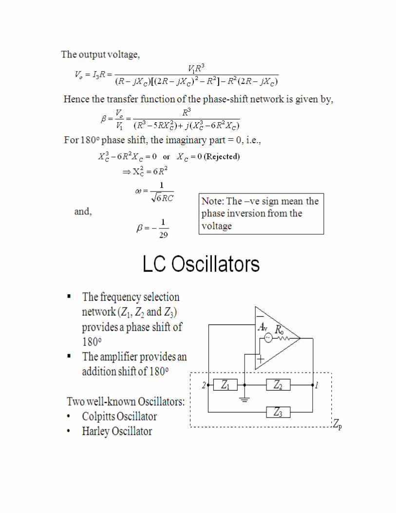
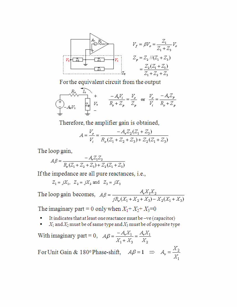


Question Bank
PART –A
1.List the two important types of RC oscillators.
2. What is the main advantage of crystal oscillator?

PART-B
o Explain the working of a transistorized Hartley oscillator. Derive expressions for
frequency of oscillation and condition for sustained oscillation.
o Draw the equivalent circuit of current amplifier with current shunt feedback and
derive expressions for (a) the output resistance with feedback Rof (b) output terminal
resistance with feedback Roft.

UNIT V
PULSE CIRCUITS AND POWER SUPPLY
RC wave shaping circuits – Diode clampers and clippers – Multivibrators – Schmitt
triggers – UJT saw-tooth oscillators – Single and poly-phase rectifiers and analysis of
filter circuits – Design of zener and transistor series voltage regulators – Switched mode
power supplies.
UNIT V
PULSE CIRCUITS AND POWER SUPPLY
Wave Shaping
The process whereby the form of a non sinusoidal signal is altered by
transmission through a linear network is called ―linear wave shaping‖. An
ideal low pass circuit is one that allows all the input frequencies below a
frequency called cutoff frequency fc and attenuates all those above this
frequency. For practical low pass circuit (Fig.1) cutoff is set to occur at a
frequency where the gain of the circuit falls by 3 dB from its maximum at
very high frequencies the capacitive reactance is very small, so the output is
almost equal to the input and hence the gain is equal to 1. Since circuit
attenuates low frequency signals and allows high frequency signals with
little or no attenuation, it is called a high pass circuit.
Circuit Diagram:
Low Pass RC Circuit :

High Pass RC Circuit :
Low Pass RC circuit frequency response

High Pass RC circuit frequency response:

CLIPPER CIRCUIT
an ideal diode with no forward voltage drop:

This circuit is not difficult to analyze if
you consider both half-cycles of the AC voltage source, one at a time.
an ideal diode with no forward voltage drop:
This circuit is not difficult to analyze if you consider both half-cycles of the
AC voltage source, one at a time.
an ideal diode with no forward voltage drop:

This circuit is not difficult to analyze if you consider both half-cycles of the
AC voltage source, one at a time.
an ideal diode with no forward voltage drop:
Predict how the operation of this clipper circuit will be affected as a result of
the following faults. Consider each fault independently (i.e. one at a time, no
multiple faults):

Diode D1 fails open:
Diode D1 fails shorted:
Resistor R1 fails open:
Resistor R1 fails shorted:
For each of these conditions, explain why the resulting effects will occur.
Diode D1 fails open: No output voltage at all.
Diode D1 fails shorted: Full AC signal at output (no clipping at all).
Resistor R1 fails open: No change (if diode is indeed ideal), but
realistically there may not be much clipping if the receiving circuit
has an extremely large input impedance.
Resistor R1 fails shorted: No output voltage at all.
predict how the operation of this clipper circuit will be affected as a result of
the following faults. Consider each fault independently (i.e. one at a time, no
multiple faults):
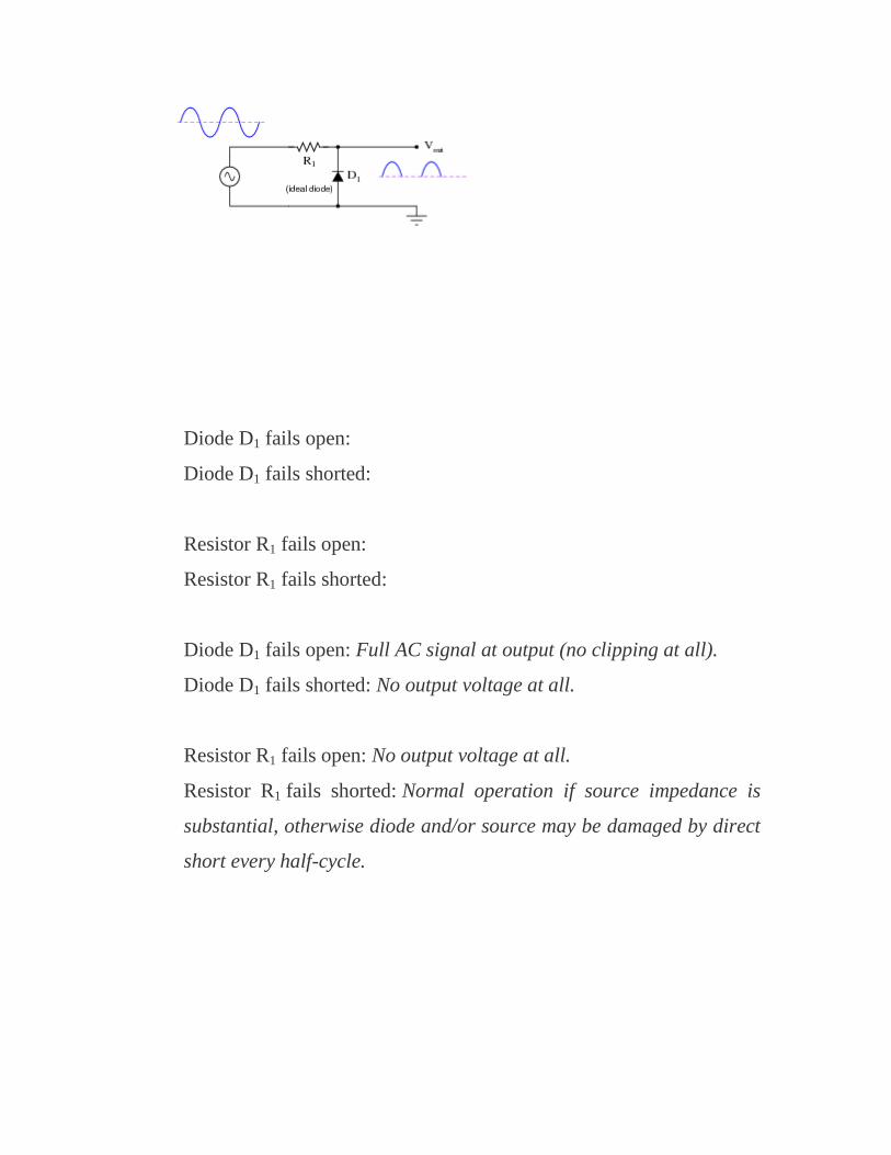
Diode D1 fails open:
Diode D1 fails shorted:
Resistor R1 fails open:
Resistor R1 fails shorted:
Diode D1 fails open: Full AC signal at output (no clipping at all).
Diode D1 fails shorted: No output voltage at all.
Resistor R1 fails open: No output voltage at all.
Resistor R1 fails shorted: Normal operation if source impedance is
substantial, otherwise diode and/or source may be damaged by direct
short every half-cycle.

CLAMPPING CIRCUIT
_
Positive voltage clamping in point A
Diode D is inversely biased, therefore it clamps positive
voltages.
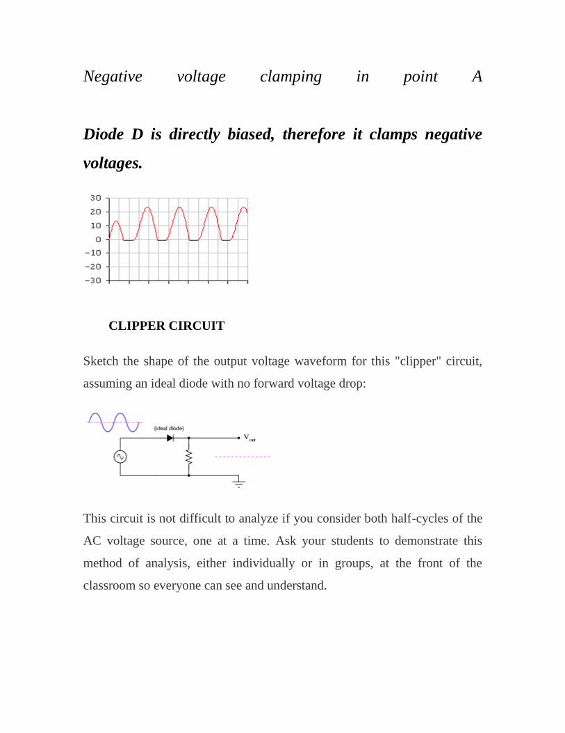
Negative voltage clamping in point A
Diode D is directly biased, therefore it clamps negative
voltages.
CLIPPER CIRCUIT
Sketch the shape of the output voltage waveform for this "clipper" circuit,
assuming an ideal diode with no forward voltage drop:
This circuit is not difficult to analyze if you consider both half-cycles of the
AC voltage source, one at a time. Ask your students to demonstrate this
method of analysis, either individually or in groups, at the front of the
classroom so everyone can see and understand.
Sketch the shape of the output voltage waveform for this "clipper" circuit,
assuming an ideal diode with no forward voltage drop:
Predict how the operation of this clipper circuit will be affected as a result of
the following faults. Consider each fault independently (i.e. one at a time, no
multiple faults):

Diode D1 fails open:
Diode D1 fails shorted:
Resistor R1 fails open:
Resistor R1 fails shorted:
For each of these conditions, explain why the resulting effects will occur.
Diode D1 fails open: No output voltage at all.
Diode D1 fails shorted: Full AC signal at output (no clipping at all).
Resistor R1 fails open: No change (if diode is indeed ideal), but
realistically there may not be much clipping if the receiving circuit
has an extremely large input impedance.
Resistor R1 fails shorted: No output voltage at all.
redict how the operation of this clipper circuit will be affected as a result of
the following faults. Consider each fault independently (i.e. one at a time, no
multiple faults):

Diode D1 fails open:
Diode D1 fails shorted:
Resistor R1 fails open:
Resistor R1 fails shorted:
Diode D1 fails open: Full AC signal at output (no clipping at all).
Diode D1 fails shorted: No output voltage at all.
Resistor R1 fails open: No output voltage at all.
Resistor R1 fails shorted: Normal operation if source impedance is
substantial, otherwise diode and/or source may be damaged by direct
short every half-cycle.
CLAMPPING CIRCUIT

_
Positive voltage clamping in point A
Diode D is inversely biased, therefore it clamps positive
voltages.

Negative voltage clamping in point A
Diode D is directly biased, therefore it clamps negative
voltages.
MULTIVIBRATOR
A multivibrator is an electronic circuit used to implement a variety of
simple two-state systems such as oscillators, timers and flip-flops. It is
characterized by two amplifying devices (transistors, electron tubes or other
devices) cross-coupled by resistors and capacitors.
There are three types of multivibrator circuit:
Astable, in which the circuit is not stable in either state—it
continuously oscillates from one state to the other. Due to this, it does
not require an input (Clock pulse or other).
Monostable, in which one of the states is stable, but the other is not—
the circuit will flip into the unstable state for a determined period, but
will eventually return to the stable state. Such a circuit is useful for

creating a timing period of fixed duration in response to some external
event. This circuit is also known as a one shot. A common application
is in eliminating switch bounce.
Bistable, in which the circuit will remain in either state indefinitely.
The circuit can be flipped from one state to the other by an external
event or trigger. Such a circuit is important as the fundamental
building block of a register or memory device. This circuit is also
known as a latch or a flip-flop.
In its simplest form the multivibrator circuit consists of two cross-coupled
transistors. Using resistor-capacitor networks within the circuit to define the
time periods of the unstable states, the various types may be implemented.
Multivibrators find applications in a variety of systems where square waves
or timed intervals are required. Simple circuits tend to be inaccurate since
many factors affect their timing, so they are rarely used where very high
precision is required.
Before the advent of low-cost integrated circuits, chains of multivibrators
found use as frequency dividers. A free-running multivibrator with a
frequency of one-half to one-tenth of the reference frequency would
accurately lock to the reference frequency. This technique was used in early
electronic organs, to keep notes of different octaves accurately in tune. Other
applications included early television systems, where the various line and
frame frequencies were kept synchronized by pulses included in the video
signal. Astable multivibrator circuit

Figure 1: Basic BJT astable multivibrator
This circuit shows a typical simple astable circuit, with an output from the
collector of Q1, and an inverted output from the collector of Q2.
Basic mode of operation
The circuit keeps one transistor switched on and the other switched off.
Suppose that initially, Q1 is switched on and Q2 is switched off.
State 1:
Q1 is on and holds the bottom of R1 near 0 V.
The right side of C1 (and the base of Q2) is being charged by R2 from
below ground to 0.6 V.
R3 is pulling the base of Q1 up, but its base-emitter diode prevents the
voltage from rising above 0.6 .
R4 is charging the right side of C2 up to the power supply voltage
(+V). Because R4 is less than R2, C2 charges faster than C1.
When the base of Q2 reaches 0.6 V, Q2 turns on, and the following positive
feedback loop occurs:

Q2 abruptly pulls the right side of C2 down to near 0 V.
Because the voltage across a capacitor cannot suddenly change, this
causes the left side of C2 to suddenly fall to almost −V, well below 0
V.
Q1 switches off due to the sudden disappearance of its base voltage.
R1 and R2 work to pull both ends of C1 toward +V, completing Q2's
turn on. The process is stopped by the B-E diode of Q2, which will
not let the right side of C1 rise very far.
This now takes us to State 2, the mirror image of the initial state, where Q1
is switched off and Q2 is switched on. Then R1 rapidly pulls C1's left side
toward +V, while R3 more slowly pulls C2's left side toward +0.6 V. When
C2's left side reaches 0.6 V, the cycle repeats.
Multivibrator frequency
The period of each half of the multivibrator is given by t = ln(2)RC. The
total period of oscillation is given by:
T = t1 + t2 = ln(2)R2 C1 + ln(2)R3 C2
Where...
f is frequency in hertz.
R2 and R3 are resistor values in ohms.
C1 and C2 are capacitor values in farads.
T is period time (In this case, the sum of two period durations).
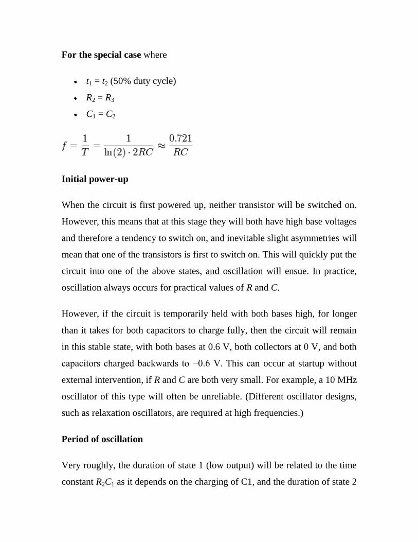
For the special case where
t1 = t2 (50% duty cycle)
R2 = R3
C1 = C2
Initial power-up
When the circuit is first powered up, neither transistor will be switched on.
However, this means that at this stage they will both have high base voltages
and therefore a tendency to switch on, and inevitable slight asymmetries will
mean that one of the transistors is first to switch on. This will quickly put the
circuit into one of the above states, and oscillation will ensue. In practice,
oscillation always occurs for practical values of R and C.
However, if the circuit is temporarily held with both bases high, for longer
than it takes for both capacitors to charge fully, then the circuit will remain
in this stable state, with both bases at 0.6 V, both collectors at 0 V, and both
capacitors charged backwards to −0.6 V. This can occur at startup without
external intervention, if R and C are both very small. For example, a 10 MHz
oscillator of this type will often be unreliable. (Different oscillator designs,
such as relaxation oscillators, are required at high frequencies.)
Period of oscillation
Very roughly, the duration of state 1 (low output) will be related to the time
constant R2C1 as it depends on the charging of C1, and the duration of state 2

(high output) will be related to the time constant R3C2 as it depends on the
charging of C2. Because they do not need to be the same, an asymmetric
duty cycle is easily achieved.
However, the duration of each state also depends on the initial state of
charge of the capacitor in question, and this in turn will depend on the
amount of discharge during the previous state, which will also depend on the
resistors used during discharge (R1 and R4) and also on the duration of the
previous state, etc. The result is that when first powered up, the period will
be quite long as the capacitors are initially fully discharged, but the period
will quickly shorten and stabilize.
The period will also depend on any current drawn from the output and on the
supply voltage.
Protective components
While not fundamental to circuit operation, diodes connected in series with
the base or emitter of the transistors are required to prevent the base-emitter
junction being driven into reverse breakdown when the supply voltage is in
excess of the Veb breakdown voltage, typically around 5-10 volts for general
purpose silicon transistors. In the monostable configuration, only one of the
transistors requires protection.
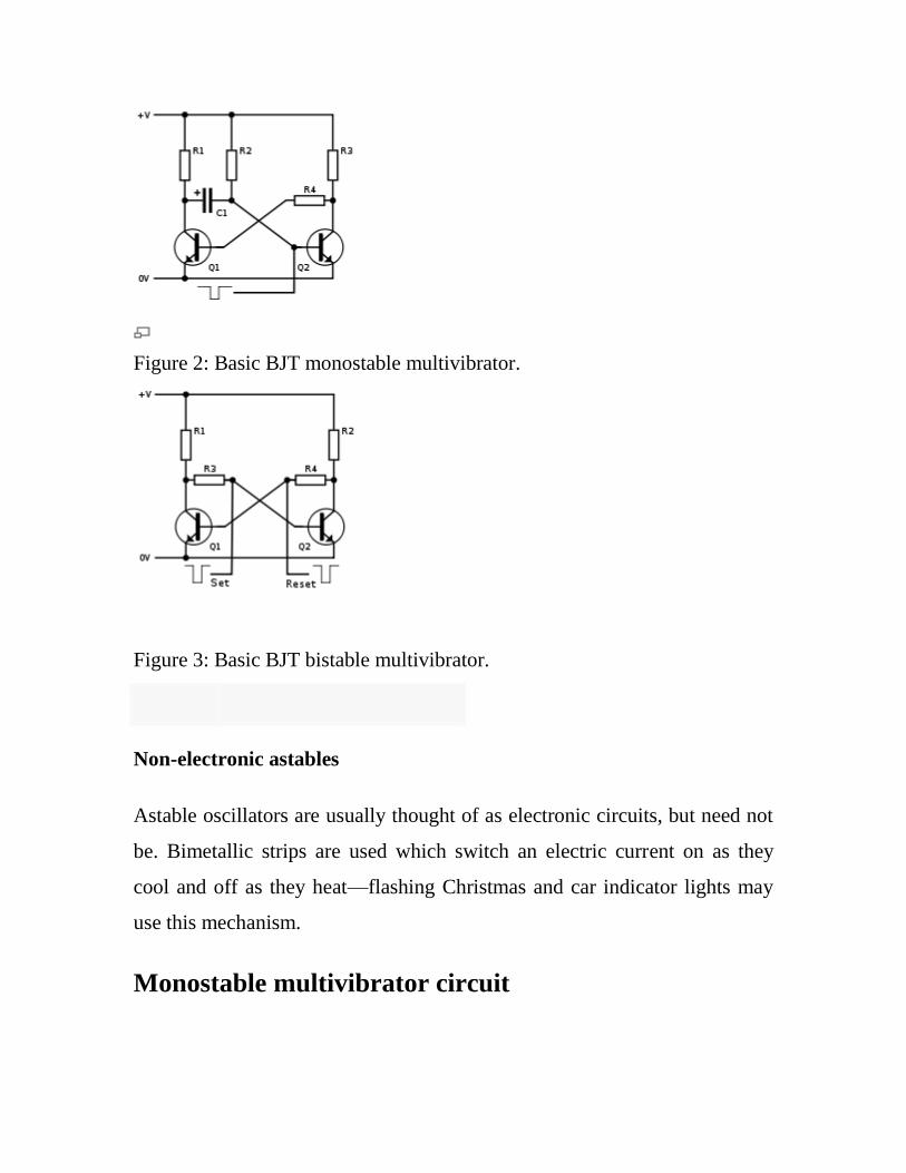
Figure 2: Basic BJT monostable multivibrator.
Figure 3: Basic BJT bistable multivibrator.
Non-electronic astables
Astable oscillators are usually thought of as electronic circuits, but need not
be. Bimetallic strips are used which switch an electric current on as they
cool and off as they heat—flashing Christmas and car indicator lights may
use this mechanism.
Monostable multivibrator circuit

When triggered by an input pulse, a monostable multivibrator will switch to
its unstable position for a period of time, and then return to its stable state.
The time period monostable multivibrator remains in unstable state is given
by t = ln(2)R2C1. If repeated application of the input pulse maintains the
circuit in the unstable state, it is called a retriggerable monostable. If further
trigger pulses do not affect the period, the circuit is a non-retriggerable
multivibrator.
Bistable multivibrator circuit
Suggested values:
R1, R2 = 10 kΩ
R3, R4 = 10 kΩ
This latch circuit is similar to an astable multivibrator, except that there is no
charge or discharge time, due to the absence of capacitors. Hence, when the
circuit is switched on, if Q1 is on, its collector is at 0 V. As a result, Q2 gets
switched off. This results in more than half +V volts being applied to R4
causing current into the base of Q1, thus keeping it on. Thus, the circuit
remains stable in a single state continuously. Similarly, Q2 remains on
continuously, if it happens to get switched on first.
Switching of state can be done via Set and Reset terminals connected to the
bases. For example, if Q2 is on and Set is grounded momentarily, this
switches Q2 off, and makes Q1 on. Thus, Set is used to "set" Q1 on, and
Reset is used to "reset" it to off state.

We've already seen one example of a monostable multivibrator in use: the
pulse detector used within the circuitry of flip-flops, to enable the latch
portion for a brief time when the clock input signal transitions from either
low to high or high to low. The pulse detector is classified as a monostable
multivibrator because it has only one stable state. By stable, I mean a state
of output where the device is able to latch or hold to forever, without
external prodding. A latch or flip-flop, being a bistable device, can hold in
either the "set" or "reset" state for an indefinite period of time. Once its set
or reset, it will continue to latch in that state unless prompted to change by
an external input. A monostable device, on the other hand, is only able to
hold in one particular state indefinitely. Its other state can only be held
momentarily when triggered by an external input.
A mechanical analogy of a monostable device would be a momentary
contact pushbutton switch, which spring-returns to its normal (stable)
position when pressure is removed from its button actuator. Likewise, a
standard wall (toggle) switch, such as the type used to turn lights on and off
in a house, is a bistable device. It can latch in one of two modes: on or off.
All monostable multivibrators are timed devices. That is, their unstable
output state will hold only for a certain minimum amount of time before
returning to its stable state. With semiconductor monostable circuits, this
timing function is typically accomplished through the use of resistors and
capacitors, making use of the exponential charging rates of RC circuits. A
comparator is often used to compare the voltage across the charging (or
discharging) capacitor with a steady reference voltage, and the on/off output
of the comparator used for a logic signal. With ladder logic, time delays are
accomplished with time-delay relays, which can be constructed with

semiconductor/RC circuits like that just mentioned, or mechanical delay
devices which impede the immediate motion of the relay's armature. Note
the design and operation of the pulse detector circuit in ladder logic:
No matter how long the input signal stays high (1), the output remains high
for just 1 second of time, then returns to its normal (stable) low state.
For some applications, it is necessary to have a monostable device that
outputs a longer pulse than the input pulse which triggers it. Consider the

following ladder logic circuit:
When the input contact closes, TD1 contact immediately closes, and stays
closed for 10 seconds after the input contact opens. No matter how short the
input pulse is, the output stays high (1) for exactly 10 seconds after the input
drops low again. This kind of monostable multivibrator is called a one-shot.
More specifically, it is a retriggerable one-shot, because the timing begins
after the input drops to a low state, meaning that multiple input pulses within
10 seconds of each other will maintain a continuous high output:

What if we only wanted a 10 second timed pulse output from a relay logic
circuit, regardless of how many input pulses we received or how long-lived
they may be? In that case, we'd have to couple a pulse-detector circuit to the
retriggerable one-shot time delay circuit, like this:
Time delay relay TD1 provides an "on" pulse to time delay relay coil TD2 for
an arbitrarily short moment (in this circuit, for at least 0.5 second each time
the input contact is actuated). As soon as TD2 is energized, the normally-
closed, timed-closed TD2 contact in series with it prevents coil TD2 from
being re-energized as long as its timing out (10 seconds). This effectively
makes it unresponsive to any more actuations of the input switch during that
10 second period.

Only after TD2 times out does the normally-closed, timed-closed TD2
contact in series with it allow coil TD2 to be energized again. This type of
one-shot is called a nonretriggerable one-shot.
One-shot multivibrators of both the retriggerable and nonretriggerable
variety find wide application in industry for siren actuation and machine
sequencing, where an intermittent input signal produces an output signal of a
set time.
Schmitt trigger with emitter-coupled transistors
Structure
Schmitt trigger implemented by two emitter-coupled transistor stages
Ii is implemented as a transistor non-inverting amplifier with positive
feedback consisting of two emitter-coupled (cascaded) transistor stages
(common-collector T2 and common-base T1) connected in a loop. There is
also a smaller negative feedback introduced by the emitter resistor RE. This

configuration can be also considered as a differential amplifier with positive
feedback between its non-inverting input (T2 base) and output (T1
collector). The chain Rc1-R1-R2 sets the base voltage for transistor T2. To
make the positive feedback dominate over the negative one and to obtain a
hysteresis, the proportion between the two collector resistors is chosen Rc1 >
Rc2. Thus less current flows through and less voltage drop is across RE when
T1 is switched than in the case when T2 is switched on. As a result, the
circuit has two different thresholds in regard to ground (V- in the picture).
Operation
Initial state. For NPN transistors as shown, imagine the input voltage is
below the shared emitter voltage (high threshold for concreteness) so that T1
base-emitter junction is backward-biased and T1 does not conduct. T2 base
voltage is determined by the mentioned divider so that T2 is conducting and
the trigger output is in the low state. The two resistors Rc2 and RE form
another voltage divider that determines the high threshold. Neglecting VBE,
the high threshold value is approximately
.
The output voltage is low but well above the ground. It is approximately
equal to the high threshold and may not be low enough to be a logical zero
for next digital circuits. This may require additional forming circuit (an
amplifier) following the trigger circuit.
Crossing up the high threshold. When the input voltage (T1 base voltage)
rises slightly above the voltage across the emitter resistor RE (the high

threshold), T1 begins conducting. Its collector voltage goes down and T2
begins going cut-off, because the voltage divider now provides lower T2
base voltage. The common emitter voltage follows this change and goes
down thus making T1 conduct more. The current begins steering from the
right leg of the circuit to the left one. Although T1 is more conducting, it
passes less current through RE (since Rc1 > Rc2); the emitter voltage
continues dropping and the effective T1 base-emitter voltage continuously
increases. This avalanche-like process continues until T1 becomes
completely turned on (saturated) and T2 turned off. The trigger is
transitioned to the high state and the output (T2 collector) voltage is close to
V+. Now, the two resistors Rc1 and RE form a voltage divider that
determines the low threshold. Its value is approximately
.
Crossing down the low threshold. With the trigger now in the high state, if
the input voltage lowers enough (below the low threshold), T1 begins to cut-
off. Its collector current reduces; as a result, the shared emitter voltage
lowers slightly and T1 collector voltage rises significantly. R1-R2 voltage
divider conveys this change to T2 base voltage and it begins conducting. The
voltage across RE rises, further reducing the T1 base-emitter potential in the
same avalanche-like manner, and T1 ceases to conduct. T2 becomes
completely turned-on (saturated) and the output voltage is low again.

Generalization
The circuit can be generalized to see the basic dynamic threshold idea
behind it. The two collector resistors Rc1 and Rc2 represent the upper legs of
a switchable voltage divider with a common lower leg (RE). T1 acts as a
comparator with a differential input (T1 base-emitter junction) consisting of
an inverting (T1 base) and a non-inverting (T1 emitter) inputs. The input
voltage is applied to the inverting input; the output voltage of the voltage
divider is applied to the non-inverting input thus determining its threshold.
The comparator output drives an electronic double throw switch (the
transistors T1 and T2) that switches over the upper legs of the voltage
divider and changes the threshold in different to the input voltage direction.
The series positive feedback forces and finishes this process.
UJT

The equivalent circuit shown in Fig.4 has been
developed to explain how the device works, and it is necessary to define the
terms used in this explanation.
RBB is known as the interbase resistance, and is the sum of RB1 and RB2:
RBB = RB1 + RB2 (1)
N.B. This is only true when the emitter is open circuit.
VRB1 is the voltage developed across RB1; this is given by the voltage divider
rule:
RB1
VRB1 = (2)
RB1 + RB2
Since the denominator of equation 2 is equal to equation 1, the former can be
rewritten as:
RB1

VRB1 = x VBB (3)
RBB
The ratio RB1 / RBB is referred to as the intrinsic standoff ratio and is denoted
by (the Greek letter eta).
If an external voltage Ve is connected to the emitter, the equivalent circuit
can be redrawn as shown in Fig.5.
If Ve is less than VRB1, the diode is reverse biased and the circuit behaves as
though the emitter was open circuit. If however Ve is increased so that it
exceeds VRB1 by at least 0.7V, the diode becomes forward biased and emitter
current Ie flows into the base 1 region. Because of this, the value of RB1
decreases. It has been suggested that this is due to the presence of additional
charge carriers (holes) in the bar. Further increase in Ve causes the emitter
current to increase which in turn reduces RB1 and this causes a further
increase in current. This runaway effect is termed regeneration. The value of
emitter voltage at which this occurs is known as the peak voltage VP and is
given by: VP = AVVBB + VD (4)
The characteristics of the UJT are illustrated by the graph of emitter voltage
against

As the emitter voltage is increased, the current is very small - just a few
microamps. When the peak point is reached, the current rises rapidly, until at
the valley point the device runs into saturation. At this point RB1 is at its
lowest value, which is known as the saturation resistance.
The simplest application of a UJT is as a relaxation oscillator, which is
defined as one in which a capacitor is charged gradually and then discharged
rapidly. The basic circuit is shown in Fig.7; in the practical circuit of Fig.8
R3 limits the emitter current and provides a voltage pulse, while R2 provides
a measure of temperature compensation. Fig. 9 shows the waveforms
occurring at the emitter and base 1; the first is an approximation to a
sawtooth and the second is a pulse of short duration.

The operation of the circuit is as follows: C1 charges through R1 until the
voltage across it reaches the peak point. The emitter current then rises
rapidly, discharging C1 through the base 1 region and R3. The sudden rise of
current through R3 produces the voltage pulse. When the current falls to IV
the UJT switches off and the cycle is repeated.
It can be shown that the time t between successive pulses is given by:
VBB - VV
t + R1C ln secs (5) N.B. R measured in Megaohms. C in µF.
VBB - VP
Single and poly-phase rectifiers and analysis of filter circuits
Rectification is the conversion of alternating current (AC) to direct current
(DC). This involves a device that only allows one-way flow of electrons. As
we have seen, this is exactly what a semiconductor diode does. The simplest

kind of rectifier circuit is the half-wave rectifier. It only allows one half of an
AC waveform to pass through to the load. (Figure below)
Half-wave rectifier circuit.
For most power applications, half-wave rectification is insufficient for the
task. The harmonic content of the rectifier‘s output waveform is very large
and consequently difficult to filter. Furthermore, the AC power source only
supplies power to the load one half every full cycle, meaning that half of its
capacity is unused. Half-wave rectification is, however, a very simple way to
reduce power to a resistive load. Some two-position lamp dimmer switches
apply full AC power to the lamp filament for ―full‖ brightness and then half-
wave rectify it for a lesser light output. (Figure below)
Half-wave rectifier application: Two level lamp dimmer.
In the ―Dim‖ switch position, the incandescent lamp receives approximately
one-half the power it would normally receive operating on full-wave AC.

Because the half-wave rectified power pulses far more rapidly than the
filament has time to heat up and cool down, the lamp does not blink. Instead,
its filament merely operates at a lesser temperature than normal, providing
less light output. This principle of ―pulsing‖ power rapidly to a slow-
responding load device to control the electrical power sent to it is common
in the world of industrial electronics. Since the controlling device (the diode,
in this case) is either fully conducting or fully nonconducting at any given
time, it dissipates little heat energy while controlling load power, making
this method of power control very energy-efficient. This circuit is perhaps
the crudest possible method of pulsing power to a load, but it suffices as a
proof-of-concept application.
If we need to rectify AC power to obtain the full use of both half-cycles of
the sine wave, a different rectifier circuit configuration must be used. Such a
circuit is called a full-wave rectifier. One kind of full-wave rectifier, called
the center-tap design, uses a transformer with a center-tapped secondary
winding and two diodes, as in Figure below.
Full-wave rectifier, center-tapped design.
This circuit‘s operation is easily understood one half-cycle at a time.
Consider the first half-cycle, when the source voltage polarity is positive (+)

on top and negative (-) on bottom. At this time, only the top diode is
conducting; the bottom diode is blocking current, and the load ―sees‖ the
first half of the sine wave, positive on top and negative on bottom. Only the
top half of the transformer‘s secondary winding carries current during this
half-cycle as in Figure below.
Full-wave center-tap rectifier: Top half of secondary winding conducts
during positive half-cycle of input, delivering positive half-cycle to load..
During the next half-cycle, the AC polarity reverses. Now, the other diode
and the other half of the transformer‘s secondary winding carry current
while the portions of the circuit formerly carrying current during the last
half-cycle sit idle. The load still ―sees‖ half of a sine wave, of the same
polarity as before: positive on top and negative on bottom. (Figure below)

Full-wave center-tap rectifier: During negative input half-cycle, bottom half
of secondary winding conducts, delivering a positive half-cycle to the load.
One disadvantage of this full-wave rectifier design is the necessity of a
transformer with a center-tapped secondary winding. If the circuit in
question is one of high power, the size and expense of a suitable transformer
is significant. Consequently, the center-tap rectifier design is only seen in
low-power applications.
The full-wave center-tapped rectifier polarity at the load may be reversed by
changing the direction of the diodes. Furthermore, the reversed diodes can
be paralleled with an existing positive-output rectifier. The result is dual-
polarity full-wave center-tapped rectifier in Figure below. Note that the
connectivity of the diodes themselves is the same configuration as a bridge.
Dual polarity full-wave center tap rectifier
Another, more popular full-wave rectifier design exists, and it is built around
a four-diode bridge configuration. For obvious reasons, this design is called
a full-wave bridge. (Figure below)

Full-wave bridge rectifier.
Current directions for the full-wave bridge rectifier circuit are as shown in
Figure below for positive half-cycle and Figure below for negative half-
cycles of the AC source waveform. Note that regardless of the polarity of the
input, the current flows in the same direction through the load. That is, the
negative half-cycle of source is a positive half-cycle at the load. The current
flow is through two diodes in series for both polarities. Thus, two diode
drops of the source voltage are lost (0.7·2=1.4 V for Si) in the diodes. This is
a disadvantage compared with a full-wave center-tap design. This
disadvantage is only a problem in very low voltage power supplies.
Full-wave bridge rectifier: Electron flow for positive half-cycles.

Full-wave bridge rectifier: Electron flow for negative half=cycles.
Remembering the proper layout of diodes in a full-wave bridge rectifier
circuit can often be frustrating to the new student of electronics. I‘ve found
that an alternative representation of this circuit is easier both to remember
and to comprehend. It‘s the exact same circuit, except all diodes are drawn
in a horizontal attitude, all ―pointing‖ the same direction. (Figure below)
Alternative layout style for Full-wave bridge rectifier.
hree-phase full-wave bridge rectifier circuit.

Each three-phase line connects between a pair of diodes: one to route power
to the positive (+) side of the load, and the other to route power to the
negative (-) side of the load. Polyphase systems with more than three phases
are easily accommodated into a bridge rectifier scheme. Take for instance
the six-phase bridge rectifier circuit in Figure below.
Six-phase full-wave bridge rectifier circuit.
When polyphase AC is rectified, the phase-shifted pulses overlap each other
to produce a DC output that is much ―smoother‖ (has less AC content) than
that produced by the rectification of single-phase AC. This is a decided
advantage in high-power rectifier circuits, where the sheer physical size of
filtering components would be prohibitive but low-noise DC power must be
obtained. The diagram in Figure below shows the full-wave rectification of
three-phase AC.
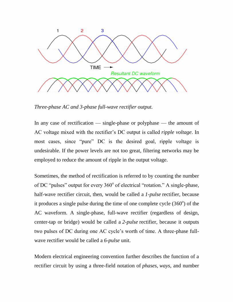
Three-phase AC and 3-phase full-wave rectifier output.
In any case of rectification — single-phase or polyphase — the amount of
AC voltage mixed with the rectifier‘s DC output is called ripple voltage. In
most cases, since ―pure‖ DC is the desired goal, ripple voltage is
undesirable. If the power levels are not too great, filtering networks may be
employed to reduce the amount of ripple in the output voltage.
Sometimes, the method of rectification is referred to by counting the number
of DC ―pulses‖ output for every 360o of electrical ―rotation.‖ A single-phase,
half-wave rectifier circuit, then, would be called a 1-pulse rectifier, because
it produces a single pulse during the time of one complete cycle (360o) of the
AC waveform. A single-phase, full-wave rectifier (regardless of design,
center-tap or bridge) would be called a 2-pulse rectifier, because it outputs
two pulses of DC during one AC cycle‘s worth of time. A three-phase full-
wave rectifier would be called a 6-pulse unit.
Modern electrical engineering convention further describes the function of a
rectifier circuit by using a three-field notation of phases, ways, and number

of pulses. A single-phase, half-wave rectifier circuit is given the somewhat
cryptic designation of 1Ph1W1P (1 phase, 1 way, 1 pulse), meaning that the
AC supply voltage is single-phase, that current on each phase of the AC
supply lines moves in only one direction (way), and that there is a single
pulse of DC produced for every 360o of electrical rotation. A single-phase,
full-wave, center-tap rectifier circuit would be designated as 1Ph1W2P in
this notational system: 1 phase, 1 way or direction of current in each
winding half, and 2 pulses or output voltage per cycle. A single-phase, full-
wave, bridge rectifier would be designated as 1Ph2W2P: the same as for the
center-tap design, except current can go both ways through the AC lines
instead of just one way. The three-phase bridge rectifier circuit shown earlier
would be called a 3Ph2W6P rectifier.
Is it possible to obtain more pulses than twice the number of phases in a
rectifier circuit? The answer to this question is yes: especially in polyphase
circuits. Through the creative use of transformers, sets of full-wave rectifiers
may be paralleled in such a way that more than six pulses of DC are
produced for three phases of AC. A 30o phase shift is introduced from
primary to secondary of a three-phase transformer when the winding
configurations are not of the same type. In other words, a transformer
connected either Y-? or ?-Y will exhibit this 30o phase shift, while a
transformer connected Y-Y or ?-? will not. This phenomenon may be
exploited by having one transformer connected Y-Y feed a bridge rectifier,
and have another transformer connected Y-? feed a second bridge rectifier,
then parallel the DC outputs of both rectifiers. (Figure below) Since the
ripple voltage waveforms of the two rectifiers‘ outputs are phase-shifted

30ofrom one another, their superposition results in less ripple than either
rectifier output considered separately: 12 pulses per 360o instead of just six:
Polyphase rectifier circuit: 3-phase 2-way 12-pulse (3Ph2W12P)
Design of zener and transistor series voltage regulators
TYPES OF VOLTAGE REGULATORS:
1) Shunt voltage regulator
2) Series voltage regulator
1) Shunt voltage regulator :
The block diagram of the shunt voltage regulator is as shown in figure.
The control element is connected in parallel with the load therefore it is
called as shunt voltage regulator. Vin is a unregulated voltage which is

obtained from rectifier o/p. The total current is shared by the load &
control element .The current flowing through control element is Ish.
Summary of regulatory action of a shunt regulator:
If output voltage increases above regulated value
▼
Feedback signal increases
▼
Control signal increases
▼
Control element draws more current
▼
Load current decreases as I is constant
▼
Output voltage is brought back to its regulated value
If output voltage decreases below regulated value
▼

Feedback signal decreases
▼
Control signal decreases
▼
Control element draws less current
▼
Load current increases as I is constant
▼
Output voltage is brought back to its regulated value
2) Series voltage regulator:
The block diagram of the series voltage regulator is shown in figure. In
this the control element is connected in series with the load therefore it is
called as series voltage regulator. As control element is in series with the
load the expression for the output voltage is given by:
Vo = Vin –
Vs
Fig: Transistor Series Voltage Regulator

Summary of regulatory action of a series regulator:
If output voltage increases above regulated value
▼
Feedback signal increases
▼
Control signal decreases
▼
Voltage across control element increases
▼
Output voltage is brought back to its regulated value
If output voltage decreases below regulated value
▼
Feedback signal decreases
▼
Control signal increases
▼
Voltage across control element decreases
▼
Output voltage is brought back to its regulated
ZENER DIODE AS A VOLTAGE REGULATOR
The voltage across zener diode is remains constant when it is operated in
zener region of reverse characteristics. This fact is utilized in applications as

a voltage regulator. Zener diode regulator is a shunt type regulator. The
reverse characteristics are shown in fig
The regulatory action can be summarized as follows:
If output voltage increases above regulated value
▼
Then I increases
▼
but IL is constant
▼
Hence Iz increases
▼
If Iz< Izmax then zener operates in the
Zener region & output voltage remains constant.
Regulating action with varying Load (constant Vin):
If RL increases then IL will decrease
▼
But I is constant & Iz = I- IL
▼
Hence Iz increases
▼
Vo is constant as long as Iz < Izmax &
Vice versa action if RL decreases.

.
ZENER DIODE AS A VOLTAGE REGULATOR
The voltage across zener diode is remains constant when it is operated in
zener region of reverse characteristics. This fact is utilized in applications
as a voltage regulator. Zener diode regulator is a shunt type regulator.
The reverse characteristics are shown in fig
Regulating action with varying input voltage(constant IL ):
We assume that RL is constant & Vin is varying. IL is also constant
because IL = Vz/ RL but supply current keeps changing due to change in
Vs.
I = Vin –Vz/Rs
*NOTES ON ZENER DIODE REGULATOR:
VZ depends on I and temperature.
Zener diodes with rated voltage < 6 V have negative temperature
coefficient; those rated > 6 V have positive temperature coefficient.
In order to maintain a constant Vo, IZT varies in response to a change
of either IL or Vi. For example, when RL increases, IL decreases, then
IZT has to increase to keep the current through Rs constant. Since the
voltage drop across Rs is constant, Vo stays constant.

SWITCHED MODE POWER SUPPLY
Theory of operation
Zener Diode Voltage Regulator
Circuit
I-V Characteristic
IZM

Block diagram of a mains operated AC–DC SMPS with output voltage
regulation
Input rectifier stage
AC, half-wave and full-wave rectified signals.
If the SMPS has an AC input, then the first stage is to convert the input to
DC. This is called rectification. The rectifier circuit can be configured as a
voltage doubler by the addition of a switch operated either manually or
automatically. This is a feature of larger supplies to permit operation from
nominally 120 V or 240 V supplies. The rectifier produces an unregulated
DC voltage which is then sent to a large filter capacitor. The current drawn
from the mains supply by this rectifier circuit occurs in short pulses around
the AC voltage peaks. These pulses have significant high frequency energy
which reduces the power factor. Special control techniques can be employed
by the following SMPS to force the average input current to follow the
sinusoidal shape of the AC input voltage thus the designer should try
correcting the power factor. An SMPS with a DC input does not require this
stage. An SMPS designed for AC input can often be run from a DC supply
(for 230 V AC this would be 330 V DC), as the DC passes through the
rectifier stage unchanged. It's however advisable to consult the manual
before trying this, though most supplies are quite capable of such operation
even though nothing is mentioned in the documentation. However, this type
of use may be harmful to the rectifier stage as it will only use half of diodes
in the rectifier for the full load. This may result in overheating of these
components, and cause them to fail prematurely. [4]
If an input range switch is used, the rectifier stage is usually configured to
operate as a voltage doubler when operating on the low voltage (~120 V
AC) range and as a straight rectifier when operating on the high voltage
(~240 V AC) range. If an input range switch is not used, then a full-wave
rectifier is usually used and the downstream inverter stage is simply
designed to be flexible enough to accept the wide range of DC voltages that
will be produced by the rectifier stage. In higher-power SMPSs, some form
of automatic range switching may be used.
Inverter stage
This section refers to the block marked chopper in the block diagram.
The inverter stage converts DC, whether directly from the input or from the
rectifier stage described above, to AC by running it through a power

oscillator, whose output transformer is very small with few windings at a
frequency of tens or hundreds of kilohertz (kHz). The frequency is usually
chosen to be above 20 kHz, to make it inaudible to humans. The output
voltage is optically coupled to the input and thus very tightly controlled. The
switching is implemented as a multistage (to achieve high gain) MOSFET
amplifier. MOSFETs are a type of transistor with a low on-resistance and a
high current-handling capacity.
Voltage converter and output rectifier
If the output is required to be isolated from the input, as is usually the case in
mains power supplies, the inverted AC is used to drive the primary winding
of a high-frequency transformer. This converts the voltage up or down to the
required output level on its secondary winding. The output transformer in
the block diagram serves this purpose.
If a DC output is required, the AC output from the transformer is rectified.
For output voltages above ten volts or so, ordinary silicon diodes are
commonly used. For lower voltages, Schottky diodes are commonly used as
the rectifier elements; they have the advantages of faster recovery times than
silicon diodes (allowing low-loss operation at higher frequencies) and a
lower voltage drop when conducting. For even lower output voltages,
MOSFETs may be used as synchronous rectifiers; compared to Schottky
diodes, these have even lower conducting state voltage drops.
The rectified output is then smoothed by a filter consisting of inductors and
capacitors. For higher switching frequencies, components with lower
capacitance and inductance are needed.

Simpler, non-isolated power supplies contain an inductor instead of a
transformer. This type includes boost converters, buck converters, and the so
called buck-boost converters. These belong to the simplest class of single
input, single output converters which use one inductor and one active switch.
The buck converter reduces the input voltage in direct proportion to the ratio
of conductive time to the total switching period, called the duty cycle. For
example an ideal buck converter with a 10 V input operating at a 50% duty
cycle will produce an average output voltage of 5 V. A feedback control
loop is employed to regulate the output voltage by varying the duty cycle to
compensate for variations in input voltage. The output voltage of a boost
converter is always greater than the input voltage and the buck-boost output
voltage is inverted but can be greater than, equal to, or less than the
magnitude of its input voltage. There are many variations and extensions to
this class of converters but these three form the basis of almost all isolated
and non-isolated DC to DC converters. By adding a second inductor the Cuk
and SEPIC converters can be implemented, or, by adding additional active
switches, various bridge converters can be realised.
Other types of SMPSs use a capacitor-diode voltage multiplier instead of
inductors and transformers. These are mostly used for generating high
voltages at low currents (Cockcroft-Walton generator). The low voltage
variant is called charge pump.
Regulation
A feedback circuit monitors the output voltage and compares it with a
reference voltage, which shown in the block diagram serves this purpose.
Depending on design/safety requirements, the controller may contain an

isolation mechanism (such as opto-couplers) to isolate it from the DC
output. Switching supplies in computers, TVs and VCRs have these opto-
couplers to tightly control the output voltage.
Open-loop regulators do not have a feedback circuit. Instead, they rely on
feeding a constant voltage to the input of the transformer or inductor, and
assume that the output will be correct. Regulated designs compensate for the
impedance of the transformer or coil. Monopolar designs also compensate
for the magnetic hysteresis of the core.
The feedback circuit needs power to run before it can generate power, so an
additional non-switching power-supply for stand-by is added.
Transformer design
SMPS transformers run at high frequency. Most of the cost savings (and
space savings) in off-line power supplies come from the fact that a high
frequency transformer is much smaller than the 50/60 Hz transformers
formerly used. There are additional design tradeoffs.
Transformer size
The higher the switching frequency, the lesser the amount of energy that
needs to be stored intermediately during the time of a single switching cycle.
Because this energy is stored in form of magnetic energy in the transformer
core material (like ferrite), less of such material is needed.
However, higher frequency also means more energy lost during transitions
of the switching semiconductor. Furthermore, much more attention to the

physical layout of the circuit board is required, and the amount of
electromagnetic interference will be more pronounced.
Core loss
There are several differences in the design of transformers for 50 Hz vs
500 kHz. Firstly a low frequency transformer usually transfers energy
through its core (soft iron), while the (usually ferrite) core of a high
frequency transformer limits leakage.
Copper loss
Main article: Copper loss
At low frequencies (such as the line frequency of 50 or 60 Hz), designers
can usually ignore the skin effect. At line frequencies, the skin effect
becomes important when the conductors have a diameter larger than about
0.3 inches (7.6 mm).
Switching power supplies must pay more attention to the skin effect because
it is a source of power loss. At 500 kHz, the skin depth is about 0.003 inches
(0.076 mm) – a dimension smaller than the typical wires used in a power
supply.

The skin effect is exacerbated by the harmonics present in the switching
waveforms. The appropriate skin depth is not just the depth at the
fundamental, but also the skin depths at the harmonics.[5]
Since the waveforms in a SMPS are generally high speed (PWM square
waves), the wiring must be capable of supporting high harmonics of the base
frequency due to skin effect.
In addition to the skin effect, there is also a proximity effect, which is
another source of power loss.
Power factor
Main article: power factor
Simple off-line switched mode power supplies incorporate a simple full
wave rectifier connected to a large energy storing capacitor. Such SMPSs
draw current from the AC line in short pulses when the mains instantaneous
voltage exceeds the voltage across this capacitor. During the remaining
portion of the AC cycle the capacitor provides energy to the power supply.
As a result, the input current of such basic switched mode power supplies
has high harmonic content and relatively low power factor. This creates
extra load on utility lines, increases heating of the utility transformers and
standard AC electric motors, and may cause stability problems in some
applications such as in emergency generator systems or aircraft generators.
Harmonics can be removed through the use of filter banks but the filtering is
expensive, and the power utility may require a business with a very low
power factor to purchase and install the filtering onsite.

Unlike displacement power factor created by linear inductive or capacitive
loads, this distortion cannot be corrected by addition of a single linear
component. Additional circuits are required to counteract the effect of the
brief current pulses.
In 2001, the European Union put into effect the standard IEC/EN61000-3-2
to set limits on the harmonics of the AC input current up to the 40th
harmonic for equipment above 75 W. The standard defines four classes of
equipment depending on its type and current waveform. The most rigorous
limits (class D) are established for personal computers, computer monitors,
and TV receivers. In order to comply with these requirements modern
switched-mode power supplies normally include an additional power factor
correction (PFC) stage.
Putting a current regulated boost chopper stage after the off-line rectifier (to
charge the storage capacitor) can correct the power factor, but increases the
complexity (and any cost).
Question Bank
PART –A
1.What is clipper?
2. What is a Schmitt trigger?
PART-B
1.(a) Explain the working of a mono-stable multi-vibrator. Draw the waveforms at the
collector and base of the transistors.
(b) Write short notes on UJT based saw-tooth oscillator.
2. (a) Explain the working of a seres voltage regulator and and perform a simplified
analysis of the same. (b) Write short notes on SMPS.

1. How a PN junction can be formed?
2. Define avalanche and zener breakdown?
3. Draw and explain the VI characteristics of pn junction diode
4. Define Reverse saturation current.
5.Define Q point.
6.what is mean by 'Thermal runaway'?
7.Define Stability factor.
8.Give the relation between the a & p . 9.Define "punch through" in early effect
1O.Draw the CE configuration.
PART-B
lla ..Explain the PN diode
(or)
b.Discuss about Zener
12.a. Explain the BIAS STABILITY
a.DC Load line b. AC Load line.
(or)
b. Explain the BIAS Compensation
a.Diode compensation b. Thermistor compensation