subject details microprocessors and microcontrollers · pdf filesubject details...
TRANSCRIPT
MPMC
3/II HAND BOOK 2013-14
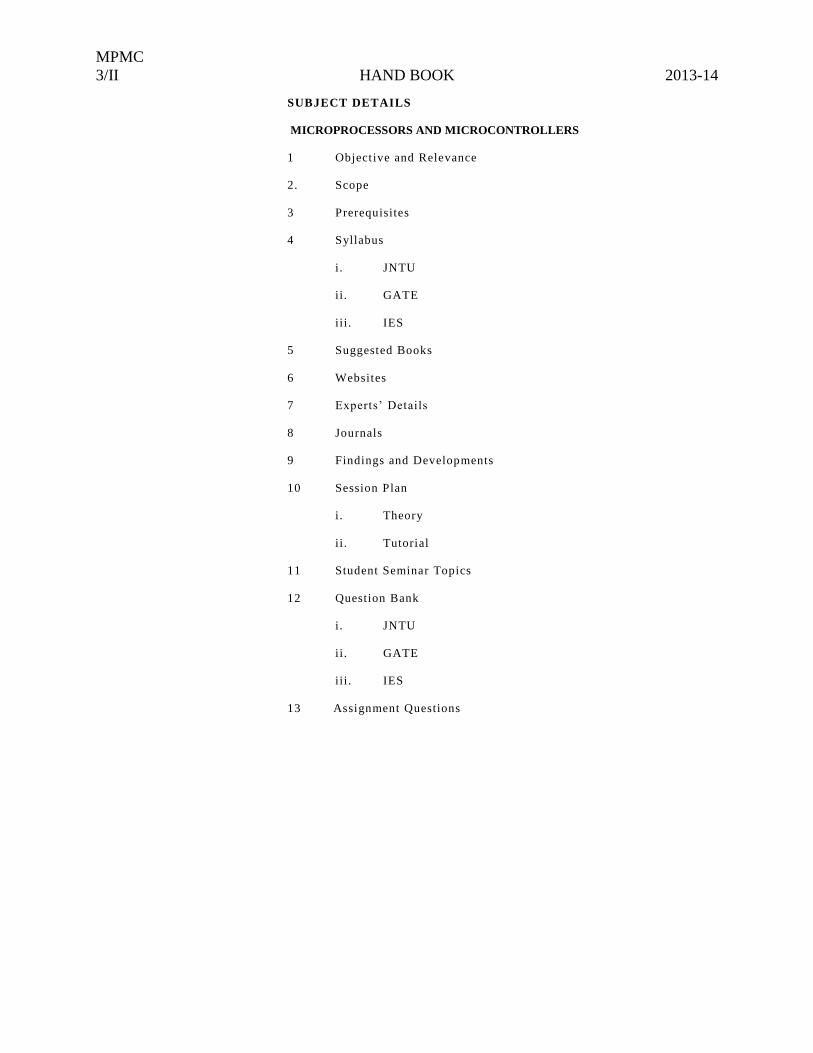
SUBJECT DETAILS
MICROPROCESSORS AND MICROCONTROLLERS
1 Objective and Relevance
2. Scope
3 Prerequisites
4 Syllabus
i . JNTU
i i . GATE
i ii . IES
5 Suggested Books
6 Websites
7 Experts’ Details
8 Journals
9 Findings and Developments
10 Session Plan
i . Theory
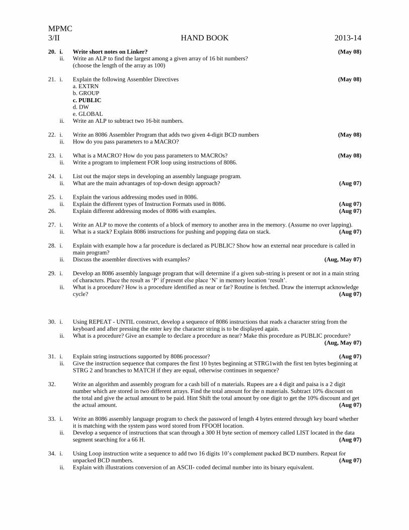
i i . Tutorial
11 Student Seminar Topics
12 Question Bank
i . JNTU
i i . GATE
i ii . IES
13 Assignment Questions
MPMC
3/II HAND BOOK 2013-14
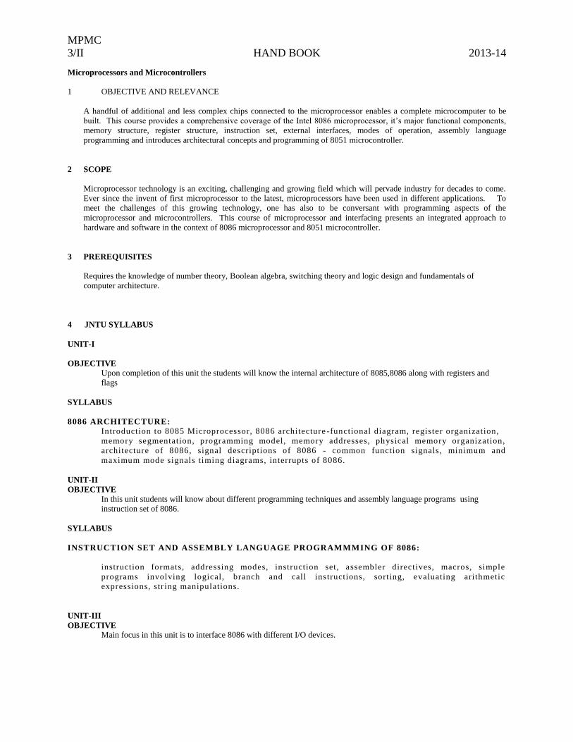
Microprocessors and Microcontrollers
1 OBJECTIVE AND RELEVANCE
A handful of additional and less complex chips connected to the microprocessor enables a complete microcomputer to be
built. This course provides a comprehensive coverage of the Intel 8086 microprocessor, it’s major functional components,
memory structure, register structure, instruction set, external interfaces, modes of operation, assembly language
programming and introduces architectural concepts and programming of 8051 microcontroller.
2 SCOPE
Microprocessor technology is an exciting, challenging and growing field which will pervade industry for decades to come.
Ever since the invent of first microprocessor to the latest, microprocessors have been used in different applications. To
meet the challenges of this growing technology, one has also to be conversant with programming aspects of the
microprocessor and microcontrollers. This course of microprocessor and interfacing presents an integrated approach to
hardware and software in the context of 8086 microprocessor and 8051 microcontroller.
3 PREREQUISITES
Requires the knowledge of number theory, Boolean algebra, switching theory and logic design and fundamentals of
computer architecture.
4 JNTU SYLLABUS
UNIT-I
OBJECTIVE
Upon completion of this unit the students will know the internal architecture of 8085,8086 along with registers and
flags
SYLLABUS
8086 ARCHITECTURE: Introduction to 8085 Microprocessor, 8086 architecture -functional diagram, register organization,
memory segmentation, programming model, memory addresses, physical memory organization,
architecture of 8086, signal descriptions of 8086 - common function signals, minimum and
maximum mode signals timing diagrams, interrupts of 8086.
UNIT-II
OBJECTIVE
In this unit students will know about different programming techniques and assembly language programs using
instruction set of 8086.
SYLLABUS
INSTRUCTION SET AND ASSEMBLY LANGUAGE PROGRAMMMING OF 8086:
instruction formats, addressing modes, instruction set, assembler directives, macros, simple
programs involving logical, branch and call instructions, sorting, evaluating arithmetic
expressions, str ing manipulations.
UNIT-III
OBJECTIVE
Main focus in this unit is to interface 8086 with different I/O devices.
MPMC
3/II HAND BOOK 2013-14
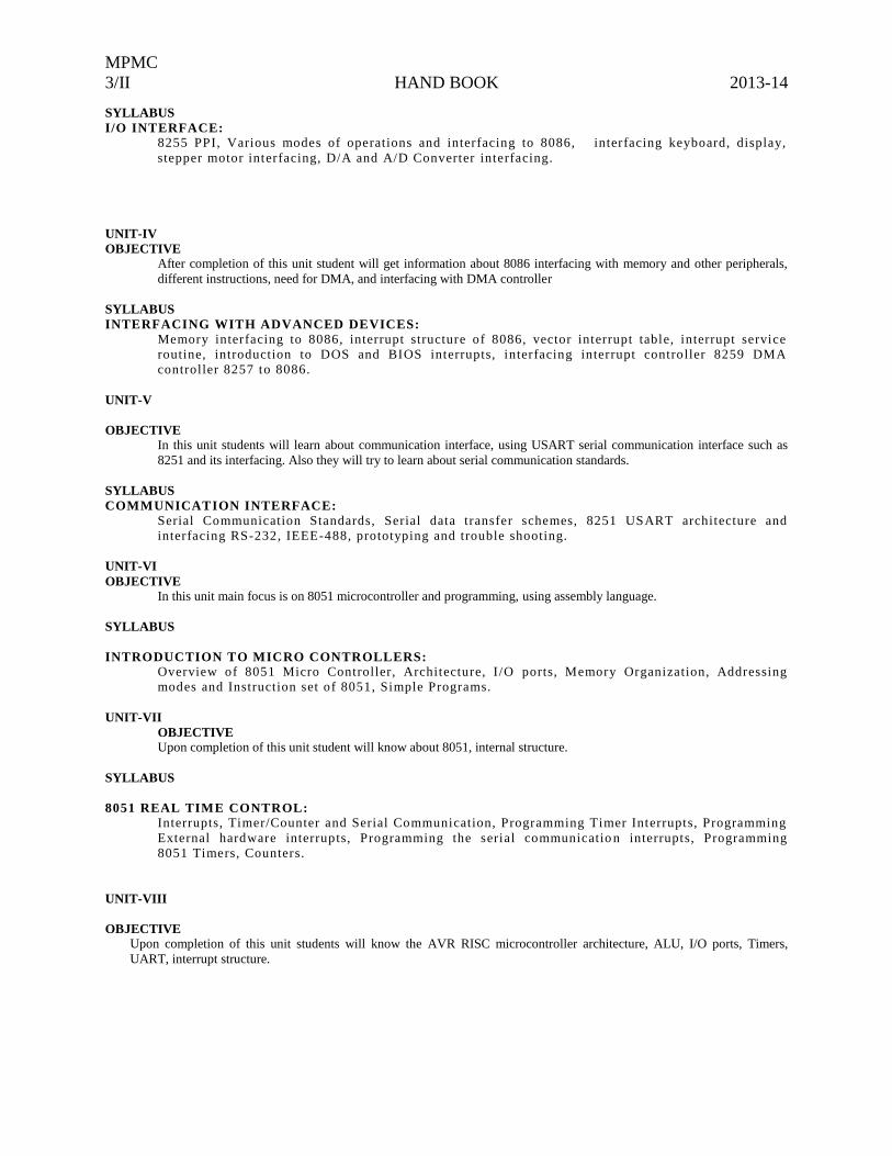
SYLLABUS
I/O INTERFACE: 8255 PPI, Various modes of operations and interfacing to 8086, interfacing keyboard, display,
stepper motor interfacing, D/A and A/D Converter interfacing.
UNIT-IV
OBJECTIVE
After completion of this unit student will get information about 8086 interfacing with memory and other peripherals,
different instructions, need for DMA, and interfacing with DMA controller
SYLLABUS
INTERFACING WITH ADVANCED DEVICES: Memory interfacing to 8086, interrupt structure of 8086, vector interrupt table, interrupt service
routine, introduction to DOS and BIOS interrupts, interfacing interrupt controller 8259 DMA
controller 8257 to 8086.
UNIT-V
OBJECTIVE
In this unit students will learn about communication interface, using USART serial communication interface such as
8251 and its interfacing. Also they will try to learn about serial communication standards.
SYLLABUS
COMMUNICATION INTERFACE: Serial Communication Standards, Serial data transfer schemes, 8251 USART architecture and
interfacing RS-232, IEEE-488, prototyping and trouble shooting.
UNIT-VI
OBJECTIVE
In this unit main focus is on 8051 microcontroller and programming, using assembly language.
SYLLABUS
INTRODUCTION TO MICRO CONTROLLERS: Overview of 8051 Micro Controller, Architecture, I /O ports, Memory Organization, Addressing
modes and Instruction set of 8051, Simple Programs.
UNIT-VII
OBJECTIVE
Upon completion of this unit student will know about 8051, internal structure.
SYLLABUS
8051 REAL TIME CONTROL: Interrupts, Timer/Counter and Serial Communication, Programming Timer Interrupts, Programming
External hardware interrupts, Programming the serial communicatio n interrupts, Programming
8051 Timers, Counters.
UNIT-VIII
OBJECTIVE Upon completion of this unit students will know the AVR RISC microcontroller architecture, ALU, I/O ports, Timers,
UART, interrupt structure.

MPMC
3/II HAND BOOK 2013-14
SYLLABUS
The AVR RISC Microcontroller architecture: Introduction, AVR family architecture, register file, the ALU, memory access and instruction
execution, I/O memory, EEPROM, I/O ports, Timers, UART, Interrupt structure.
2 GATE SYLLABUS
Unit I
Microprocessor (8085) architecture, programming, memory and I/O interfacing.
Unit II—VIII
NOT APPLICABLE
Unit III
NOT APPLICABLE
Unit III
NOT APPLICABLE
Unit IV
NOT APPLICABLE
Unit V
NOT APPLICABLE
Unit VI
NOT APPLICABLE
Unit VII
NOT APPLICABLE
Unit VIII
NOT APPLICABLE
3 IES SYLLABUS
Unit I
Architecture and instruction set of Microprocessors 8085, Assembly language Programming.
Architecture of Microprocessors 8086.
Unit II
instruction set of Microprocessors 8086, Assembly language Programming
Unit III
NOT APPLICABLE
Unit III
NOT APPLICABLE
Unit IV
NOT APPLICABLE
Unit V
NOT APPLICABLE
Unit VI
NOT APPLICABLE
Unit VII
NOT APPLICABLE
Unit VIII
NOT APPLICABLE
MPMC
3/II HAND BOOK 2013-14
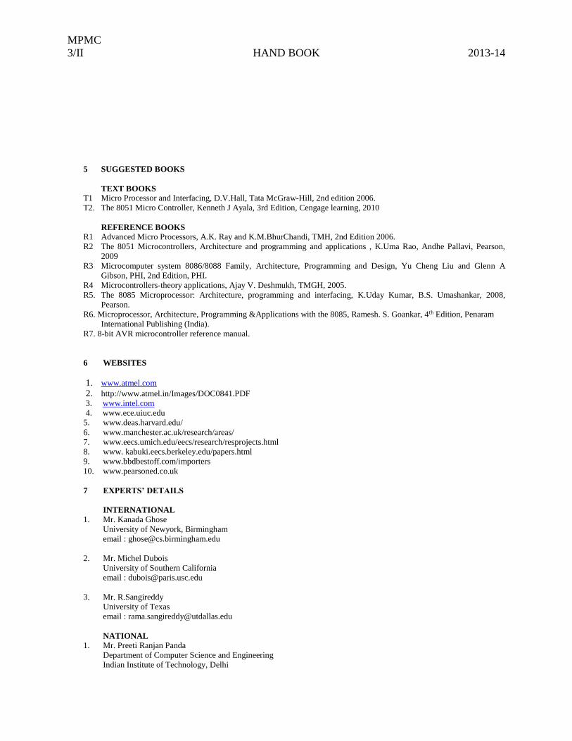
5 SUGGESTED BOOKS
TEXT BOOKS T1 Micro Processor and Interfacing, D.V.Hall, Tata McGraw-Hill, 2nd edition 2006.
T2. The 8051 Micro Controller, Kenneth J Ayala, 3rd Edition, Cengage learning, 2010
REFERENCE BOOKS
R1 Advanced Micro Processors, A.K. Ray and K.M.BhurChandi, TMH, 2nd Edition 2006.
R2 The 8051 Microcontrollers, Architecture and programming and applications , K.Uma Rao, Andhe Pallavi, Pearson,
2009
R3 Microcomputer system 8086/8088 Family, Architecture, Programming and Design, Yu Cheng Liu and Glenn A
Gibson, PHI, 2nd Edition, PHI.
R4 Microcontrollers-theory applications, Ajay V. Deshmukh, TMGH, 2005.
R5. The 8085 Microprocessor: Architecture, programming and interfacing, K.Uday Kumar, B.S. Umashankar, 2008,
Pearson.
R6. Microprocessor, Architecture, Programming &Applications with the 8085, Ramesh. S. Goankar, 4th Edition, Penaram
International Publishing (India).
R7. 8-bit AVR microcontroller reference manual.
6 WEBSITES
1. www.atmel.com
2. http://www.atmel.in/Images/DOC0841.PDF
3. www.intel.com
4. www.ece.uiuc.edu
5. www.deas.harvard.edu/
6. www.manchester.ac.uk/research/areas/
7. www.eecs.umich.edu/eecs/research/resprojects.html
8. www. kabuki.eecs.berkeley.edu/papers.html
9. www.bbdbestoff.com/importers
10. www.pearsoned.co.uk
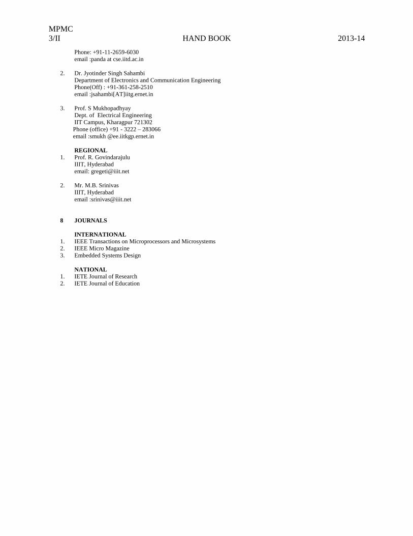
7 EXPERTS’ DETAILS
INTERNATIONAL 1. Mr. Kanada Ghose
University of Newyork, Birmingham
email : [email protected]
2. Mr. Michel Dubois
University of Southern California
email : [email protected]
3. Mr. R.Sangireddy
University of Texas
email : [email protected]
NATIONAL
1. Mr. Preeti Ranjan Panda
Department of Computer Science and Engineering
Indian Institute of Technology, Delhi
MPMC
3/II HAND BOOK 2013-14
Phone: +91-11-2659-6030
email :panda at cse.iitd.ac.in
2. Dr. Jyotinder Singh Sahambi
Department of Electronics and Communication Engineering
Phone(Off) : +91-361-258-2510
email :jsahambi[AT]iitg.ernet.in
3. Prof. S Mukhopadhyay
Dept. of Electrical Engineering
IIT Campus, Kharagpur 721302
Phone (office) +91 - 3222 – 283066
email :smukh @ee.iitkgp.ernet.in
REGIONAL 1. Prof. R. Govindarajulu
IIIT, Hyderabad
email: [email protected]
2. Mr. M.B. Srinivas
IIIT, Hyderabad
email :[email protected]
8 JOURNALS
INTERNATIONAL
1. IEEE Transactions on Microprocessors and Microsystems
2. IEEE Micro Magazine
3. Embedded Systems Design
NATIONAL
1. IETE Journal of Research
2. IETE Journal of Education
MPMC
3/II HAND BOOK 2013-14
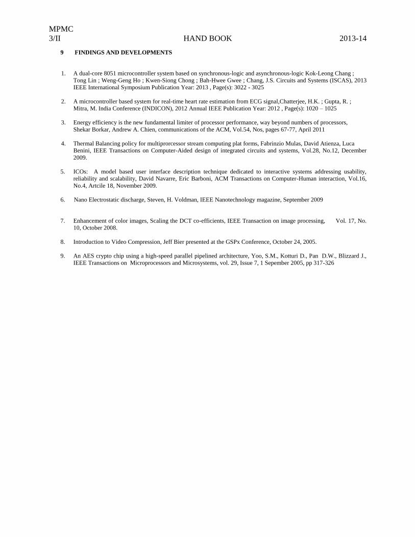
9 FINDINGS AND DEVELOPMENTS
1. A dual-core 8051 microcontroller system based on synchronous-logic and asynchronous-logic Kok-Leong Chang ;
Tong Lin ; Weng-Geng Ho ; Kwen-Siong Chong ; Bah-Hwee Gwee ; Chang, J.S. Circuits and Systems (ISCAS), 2013
IEEE International Symposium Publication Year: 2013 , Page(s): 3022 - 3025
2. A microcontroller based system for real-time heart rate estimation from ECG signal,Chatterjee, H.K. ; Gupta, R. ;
Mitra, M. India Conference (INDICON), 2012 Annual IEEE Publication Year: 2012 , Page(s): 1020 – 1025
3. Energy efficiency is the new fundamental limiter of processor performance, way beyond numbers of processors,
Shekar Borkar, Andrew A. Chien, communications of the ACM, Vol.54, Nos, pages 67-77, April 2011
4. Thermal Balancing policy for multiprorcessor stream computing plat forms, Fabrinzio Mulas, David Atienza, Luca
Benini, IEEE Transactions on Computer-Aided design of integrated circuits and systems, Vol.28, No.12, December
2009.
5. ICOs: A model based user interface description technique dedicated to interactive systems addressing usability,
reliability and scalability, David Navarre, Eric Barboni, ACM Transactions on Computer-Human interaction, Vol.16,
No.4, Artcile 18, November 2009.
6. Nano Electrostatic discharge, Steven, H. Voldman, IEEE Nanotechnology magazine, September 2009
7. Enhancement of color images, Scaling the DCT co-efficients, IEEE Transaction on image processing, Vol. 17, No.
10, October 2008.
8. Introduction to Video Compression, Jeff Bier presented at the GSPx Conference, October 24, 2005.
9. An AES crypto chip using a high-speed parallel pipelined architecture, Yoo, S.M., Kotturi D., Pan D.W., Blizzard J.,
IEEE Transactions on Microprocessors and Microsystems, vol. 29, Issue 7, 1 Sepember 2005, pp 317-326
MPMC
3/II HAND BOOK 2013-14
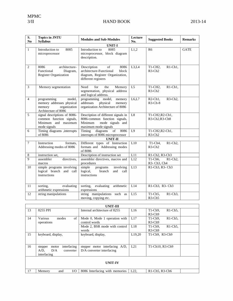
S.
No
Topics in JNTU
Syllabus Modules and Sub-Modules
Lecture
No. Suggested Books Remarks
UNIT-I
1 Introduction to 8085
microprocessor
Introduction to 8085
microprocessor, block diagram
description.
L1,2 R6 GATE
2
8086 architecture-
Functional Diagram,
Register Organization
Description of 8086
architecture-Functional block
diagram, Register Organization,
different registers
L3,L4 T1-CH2, R1-Ch1,
R3-Ch2
3 Memory segmentation Need for the Memory
segmentation, physical address
and logical address.
L5 T1-CH2, R1-Ch1,
R3-Ch2
4 programming model,
memory addresses physical
memory organization
Architecture of 8086
programming model, memory
addresses physical memory
organization Architecture of 8086
L6,L7 R2-Ch1, R3-Ch2,
R3-Ch-8
5 signal descriptions of 8086-
common function signals,
Minimum and maximum
mode signals
Description of different signals in
8086-common function signals,
Minimum mode signals and
maximum mode signals
L8 T1-CH2,R2-Ch1,
R3-Ch2,R3-Ch8
6 Timing diagrams ,interrupts
of 8086
Timing diagrams of 8086
interrupts of 8086 microprocessor
L9 T1-CH2,R2-Ch1,
R3-Ch2
UNIT-II
7 Instruction formats,
Addressing modes of 8086
Different types of Instruction
formats and Addressing modes
of 8086
L10 T1-Ch4, R1-Ch2,
R3-Ch2
8 instruction set, Description of instruction set L11 R1-Ch2, R3-Ch3
9 assembler directives,
macros
assembler directives, macros and
procedures
L12 T1-Ch6, R1-Ch2,
R3- Ch3, Ch4
10 simple programs involving
logical branch and call
instructions
simple programs involving
logical, branch and call
instructions
L13 R1-Ch3, R3- Ch3
11 sorting, evaluating
arithmetic expressions
sorting, evaluating arithmetic
expressions
L14 R1-Ch3, R3- Ch3
12 string manipulations string manipulations such as
moving, copying etc.
L15 T1-Ch5, R1-Ch3,
R3-Ch5
UNIT-III
13 8255 PPI Internal architecture of 8255 L16 T1-Ch9, R1-Ch5,
R3-Ch9
14 Various modes of
operations
Mode 0, Mode 1 operation with
control words
L17 T1-Ch9, R1-Ch5,
R3-Ch9
Mode 2, BSR mode with control
words
L18 T1-Ch9, R1-Ch5,
R3-Ch9
15 keyboard, display, keyboard, display, L19,20 T1-Ch9, R3-Ch9
16 stepper motor interfacing
A/D, D/A converter
interfacing
stepper motor interfacing A/D,
D/A converter interfacing
L21 T1-Ch10, R3-Ch9
UNIT-IV
17 Memory and I/O 8086 Interfacing with memories L22, R1-Ch5, R3-Ch6
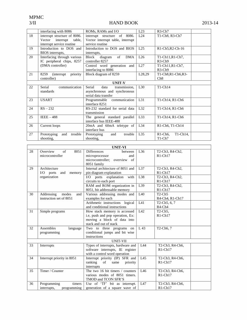
MPMC
3/II HAND BOOK 2013-14
interfacing with 8086 ROMs, RAMs and I/O L23 R3-Ch7
18 interrupt structure of 8086.
Vector interrupt table,
interrupt service routine
interrupt structure of 8086.
Vector interrupt table, interrupt
service routine
L24 T1-Ch8, R3-Ch7
19 Introduction to DOS and
BIOS interrupts,
Introduction to DOS and BIOS
interrupts,
L25 R1-Ch5,R2-Ch-16
20 Interfacing through various
IC peripheral chips, 8257
(DMA controller)
Block diagram of DMA
controller 8257
L26 T1-Ch11,R1-Ch7,
R3-Ch9
Control word generation and
interfacing to 8086
L27 T1-Ch11,R1-Ch7,
R3-Ch9
21 8259 (interrupt priority
controller)
Block diagram of 8259 L28,29 T1-Ch8,R1-Ch6,R3-
Ch8
UNIT-V
22 Serial communication
standards
Serial data transmission,
asynchronous and synchronous
serial data transfer
L30 T1-Ch14
23 USART Programmable communication
interface 8251
L31 T1-Ch14, R1-Ch6
24 RS – 232 RS-232 standard for serial data
transmission
L32 T1-Ch14, R1-Ch6
25 IEEE – 488 The general standard parallel
interface bus IEEE-488
L33 T1-Ch14, R1-Ch6
26 Current loops 20mA and 60mA teletype of
interface bus
L34 R1-Ch6, T1-Ch14
27 Prototyping and trouble
shooting,
Prototyping and trouble
shooting,
L35 R1-Ch6, T1-Ch14,
T1-Ch7
UNIT-VI
28 Overview of 8051
microcontroller
Differences between
microprocessor and
microcontroller; overview of
8051 family
L36
T2-Ch3, R4-Ch2,
R1-Ch17
29 Architecture
I/O ports and memory
organization
Internal architecture of 8051 and
pin diagram explanation
L37 T2-Ch3, R4-Ch2,
R1-Ch17
I/O ports explanation with
circuits to each port
L38 T2-Ch3, R4-Ch2,
R1-Ch17
RAM and ROM organization in
8051, bit addressable memory
L39 T2-Ch3, R4-Ch2,
R1-Ch17
30 Addressing modes and
instruction set of 8051
Various addressing modes and
examples for each
L40 T2-Ch5
R4-Ch4, R1-Ch17
Arithmetic instructions logical
and conditional instructions
L41 T2-Ch5, 6, 7
R4-Ch4
31 Simple programs How stack memory is accessed
i.e, push and pop operation, Ex:
moving a block of data into
stack and out of stack
L42 T2-Ch5,
R1-Ch17
32 Assembles language
programming
Two to three programs on
conditional jumps and bit wise
instructions
L 43 T2-Ch6, 7
UNIT-VII
33 Interrupts Types of interrupts, hardware and
software interrupts, IE register
with a control word operation
L44 T2-Ch3, R4-Ch6,
R1-Ch17
34 Interrupt priority in 8051 Interrupt priority (IP) SFR and
ranking of same priority
interrupts
L45 T2-Ch3, R4-Ch6,
R1-Ch17
35 Timer / Counter The two 16 bit timers / counters
various modes of 8051 timers.
TMOD and TCON SFR’S
L46 T2-Ch3, R4-Ch6,
R1-Ch17
36 Programming timers
interrupts, programming
Use of ‘TF’ bit as interrupt.
generation of a square wave of
L47 T2-Ch3, R4-Ch6,
R1-Ch17
MPMC
3/II HAND BOOK 2013-14
timers / counters desired duty cycle using timer /
counters
37 Serial communication
programming the serial
communication interrupts
SBUF, SCON and PCON SFRS
control word explanation.
Example program for transfer of
data serially and also to receive
data serially
L48 T2-Ch3, R4-Ch6,
R1-Ch17
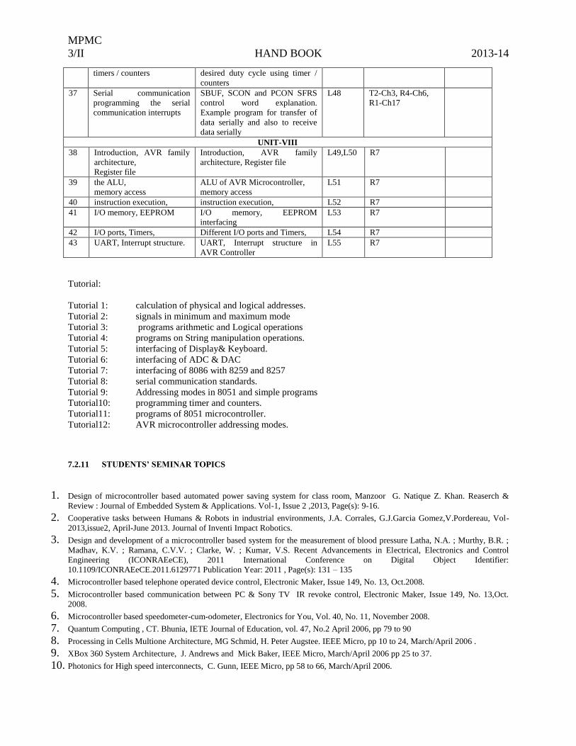
UNIT-VIII
38 Introduction, AVR family
architecture,
Register file
Introduction, AVR family
architecture, Register file
L49,L50 R7
39 the ALU,
memory access
ALU of AVR Microcontroller,
memory access
L51 R7
40 instruction execution, instruction execution, L52 R7
41 I/O memory, EEPROM I/O memory, EEPROM
interfacing
L53 R7
42 I/O ports, Timers, Different I/O ports and Timers, L54 R7
43 UART, Interrupt structure. UART, Interrupt structure in
AVR Controller
L55 R7
Tutorial:
Tutorial 1: calculation of physical and logical addresses.
Tutorial 2: signals in minimum and maximum mode
Tutorial 3: programs arithmetic and Logical operations
Tutorial 4: programs on String manipulation operations.
Tutorial 5: interfacing of Display& Keyboard.
Tutorial 6: interfacing of ADC & DAC
Tutorial 7: interfacing of 8086 with 8259 and 8257
Tutorial 8: serial communication standards.
Tutorial 9: Addressing modes in 8051 and simple programs
Tutorial10: programming timer and counters.
Tutorial11: programs of 8051 microcontroller.
Tutorial12: AVR microcontroller addressing modes.
7.2.11 STUDENTS’ SEMINAR TOPICS
1. Design of microcontroller based automated power saving system for class room, Manzoor G. Natique Z. Khan. Reaserch &
Review : Journal of Embedded System & Applications. Vol-1, Issue 2 ,2013, Page(s): 9-16.
2. Cooperative tasks between Humans & Robots in industrial environments, J.A. Corrales, G.J.Garcia Gomez,V.Pordereau, Vol-
2013,issue2, April-June 2013. Journal of Inventi Impact Robotics.
3. Design and development of a microcontroller based system for the measurement of blood pressure Latha, N.A. ; Murthy, B.R. ;
Madhav, K.V. ; Ramana, C.V.V. ; Clarke, W. ; Kumar, V.S. Recent Advancements in Electrical, Electronics and Control
Engineering (ICONRAEeCE), 2011 International Conference on Digital Object Identifier:
10.1109/ICONRAEeCE.2011.6129771 Publication Year: 2011 , Page(s): 131 – 135
4. Microcontroller based telephone operated device control, Electronic Maker, Issue 149, No. 13, Oct.2008.
5. Microcontroller based communication between PC & Sony TV IR revoke control, Electronic Maker, Issue 149, No. 13,Oct.
2008.
6. Microcontroller based speedometer-cum-odometer, Electronics for You, Vol. 40, No. 11, November 2008.
7. Quantum Computing , CT. Bhunia, IETE Journal of Education, vol. 47, No.2 April 2006, pp 79 to 90
8. Processing in Cells Multione Architecture, MG Schmid, H. Peter Augstee. IEEE Micro, pp 10 to 24, March/April 2006 .
9. XBox 360 System Architecture, J. Andrews and Mick Baker, IEEE Micro, March/April 2006 pp 25 to 37.
10. Photonics for High speed interconnects, C. Gunn, IEEE Micro, pp 58 to 66, March/April 2006.
MPMC
3/II HAND BOOK 2013-14
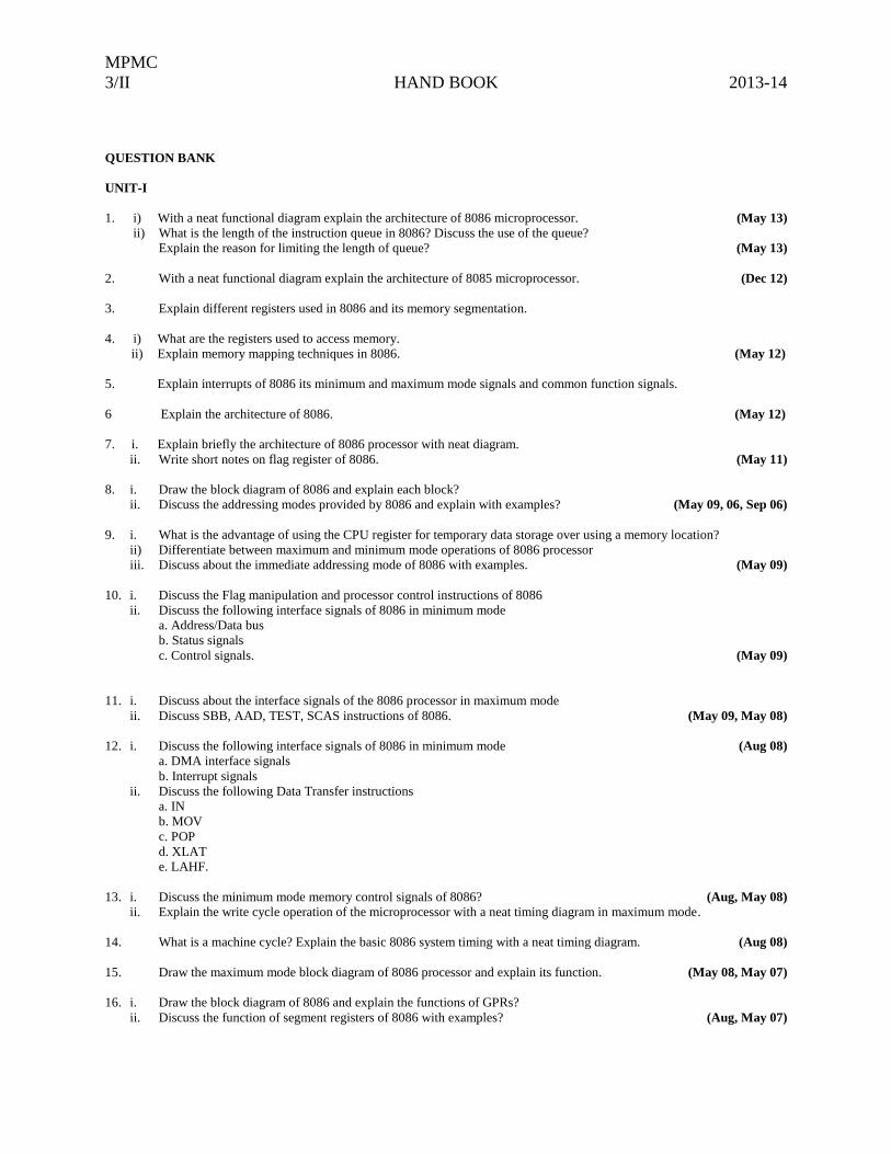
QUESTION BANK
UNIT-I
1. i) With a neat functional diagram explain the architecture of 8086 microprocessor. (May 13)
ii) What is the length of the instruction queue in 8086? Discuss the use of the queue?
Explain the reason for limiting the length of queue? (May 13)
2. With a neat functional diagram explain the architecture of 8085 microprocessor. (Dec 12)
3. Explain different registers used in 8086 and its memory segmentation.
4. i) What are the registers used to access memory. (May12)
ii) Explain memory mapping techniques in 8086. (May 12)
5. Explain interrupts of 8086 its minimum and maximum mode signals and common function signals.
6 Explain the architecture of 8086. (May 12)
7. i. Explain briefly the architecture of 8086 processor with neat diagram.
ii. Write short notes on flag register of 8086. (May 11)
8. i. Draw the block diagram of 8086 and explain each block?
ii. Discuss the addressing modes provided by 8086 and explain with examples? (May 09, 06, Sep 06)
9. i. What is the advantage of using the CPU register for temporary data storage over using a memory location?
ii) Differentiate between maximum and minimum mode operations of 8086 processor
iii. Discuss about the immediate addressing mode of 8086 with examples. (May 09)
10. i. Discuss the Flag manipulation and processor control instructions of 8086
ii. Discuss the following interface signals of 8086 in minimum mode
a. Address/Data bus
b. Status signals
c. Control signals. (May 09)
11. i. Discuss about the interface signals of the 8086 processor in maximum mode
ii. Discuss SBB, AAD, TEST, SCAS instructions of 8086. (May 09, May 08)
12. i. Discuss the following interface signals of 8086 in minimum mode (Aug 08)
a. DMA interface signals
b. Interrupt signals
ii. Discuss the following Data Transfer instructions
a. IN
b. MOV
c. POP
d. XLAT
e. LAHF.
13. i. Discuss the minimum mode memory control signals of 8086? (Aug, May 08)
ii. Explain the write cycle operation of the microprocessor with a neat timing diagram in maximum mode.
14. What is a machine cycle? Explain the basic 8086 system timing with a neat timing diagram. (Aug 08)
15. Draw the maximum mode block diagram of 8086 processor and explain its function. (May 08, May 07)
16. i. Draw the block diagram of 8086 and explain the functions of GPRs?
ii. Discuss the function of segment registers of 8086 with examples? (Aug, May 07)
MPMC
3/II HAND BOOK 2013-14
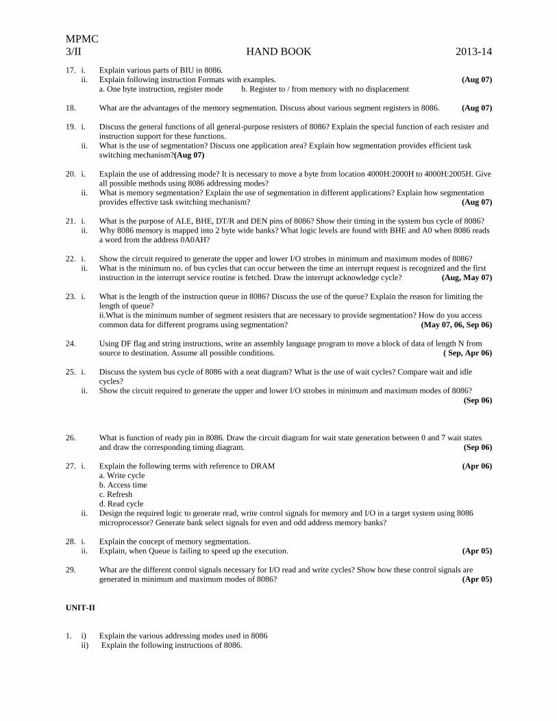
17. i. Explain various parts of BIU in 8086.
ii. Explain following instruction Formats with examples. (Aug 07)
a. One byte instruction, register mode b. Register to / from memory with no displacement
18. What are the advantages of the memory segmentation. Discuss about various segment registers in 8086. (Aug 07)
19. i. Discuss the general functions of all general-purpose resisters of 8086? Explain the special function of each resister and
instruction support for these functions.
ii. What is the use of segmentation? Discuss one application area? Explain how segmentation provides efficient task
switching mechanism?(Aug 07)
20. i. Explain the use of addressing mode? It is necessary to move a byte from location 4000H:2000H to 4000H:2005H. Give
all possible methods using 8086 addressing modes?
ii. What is memory segmentation? Explain the use of segmentation in different applications? Explain how segmentation
provides effective task switching mechanism? (Aug 07)
21. i. What is the purpose of ALE, BHE, DT/R and DEN pins of 8086? Show their timing in the system bus cycle of 8086? (Aug, May 07)
ii. Why 8086 memory is mapped into 2 byte wide banks? What logic levels are found with BHE and A0 when 8086 reads
a word from the address 0A0AH?
22. i. Show the circuit required to generate the upper and lower I/O strobes in minimum and maximum modes of 8086?
ii. What is the minimum no. of bus cycles that can occur between the time an interrupt request is recognized and the first
instruction in the interrupt service routine is fetched. Draw the interrupt acknowledge cycle? (Aug, May 07)
23. i. What is the length of the instruction queue in 8086? Discuss the use of the queue? Explain the reason for limiting the
length of queue?
ii.What is the minimum number of segment resisters that are necessary to provide segmentation? How do you access
common data for different programs using segmentation? (May 07, 06, Sep 06)
24. Using DF flag and string instructions, write an assembly language program to move a block of data of length N from
source to destination. Assume all possible conditions. ( Sep, Apr 06)
25. i. Discuss the system bus cycle of 8086 with a neat diagram? What is the use of wait cycles? Compare wait and idle
cycles?
ii. Show the circuit required to generate the upper and lower I/O strobes in minimum and maximum modes of 8086?
(Sep 06)
26. What is function of ready pin in 8086. Draw the circuit diagram for wait state generation between 0 and 7 wait states
and draw the corresponding timing diagram. (Sep 06)
27. i. Explain the following terms with reference to DRAM (Apr 06)
a. Write cycle
b. Access time
c. Refresh
d. Read cycle
ii. Design the required logic to generate read, write control signals for memory and I/O in a target system using 8086
microprocessor? Generate bank select signals for even and odd address memory banks?
28. i. Explain the concept of memory segmentation.
ii. Explain, when Queue is failing to speed up the execution. (Apr 05)
29. What are the different control signals necessary for I/O read and write cycles? Show how these control signals are
generated in minimum and maximum modes of 8086? (Apr 05)
UNIT-II
1. i) Explain the various addressing modes used in 8086
ii) Explain the following instructions of 8086.
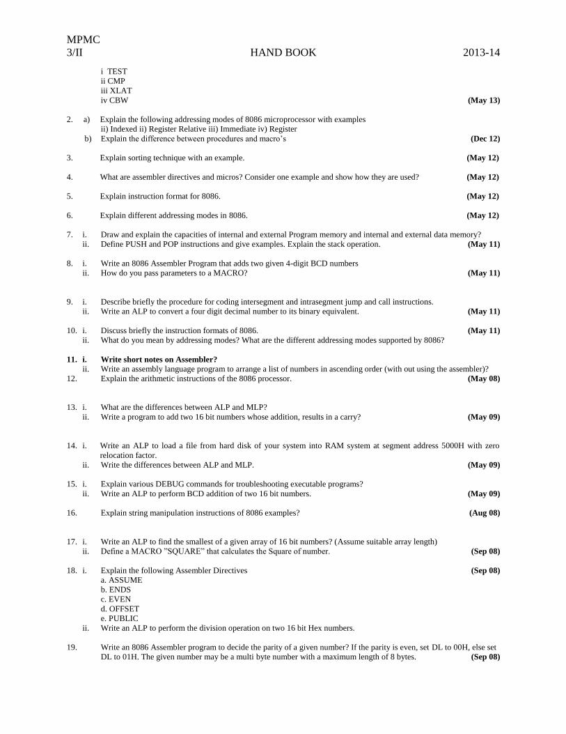
MPMC
3/II HAND BOOK 2013-14
i TEST
ii CMP
iii XLAT
iv CBW (May 13)
2. a) Explain the following addressing modes of 8086 microprocessor with examples
ii) Indexed ii) Register Relative iii) Immediate iv) Register
b) Explain the difference between procedures and macro’s (Dec 12)
3. Explain sorting technique with an example. (May 12)
4. What are assembler directives and micros? Consider one example and show how they are used? (May 12)
5. Explain instruction format for 8086. (May 12)
6. Explain different addressing modes in 8086. (May 12)
7. i. Draw and explain the capacities of internal and external Program memory and internal and external data memory?
ii. Define PUSH and POP instructions and give examples. Explain the stack operation. (May 11)
8. i. Write an 8086 Assembler Program that adds two given 4-digit BCD numbers
ii. How do you pass parameters to a MACRO? (May 11)
9. i. Describe briefly the procedure for coding intersegment and intrasegment jump and call instructions.
ii. Write an ALP to convert a four digit decimal number to its binary equivalent. (May 11)
10. i. Discuss briefly the instruction formats of 8086. (May 11)
ii. What do you mean by addressing modes? What are the different addressing modes supported by 8086?
11. i. Write short notes on Assembler?
ii. Write an assembly language program to arrange a list of numbers in ascending order (with out using the assembler)? (May 09, Sep 08)
12. Explain the arithmetic instructions of the 8086 processor. (May 08)
13. i. What are the differences between ALP and MLP?
ii. Write a program to add two 16 bit numbers whose addition, results in a carry? (May 09)
14. i. Write an ALP to load a file from hard disk of your system into RAM system at segment address 5000H with zero
relocation factor.
ii. Write the differences between ALP and MLP. (May 09)
15. i. Explain various DEBUG commands for troubleshooting executable programs?
ii. Write an ALP to perform BCD addition of two 16 bit numbers. (May 09)
16. Explain string manipulation instructions of 8086 examples? (Aug 08)
17. i. Write an ALP to find the smallest of a given array of 16 bit numbers? (Assume suitable array length)
ii. Define a MACRO ”SQUARE” that calculates the Square of number. (Sep 08)
18. i. Explain the following Assembler Directives (Sep 08)
a. ASSUME
b. ENDS
c. EVEN
d. OFFSET
e. PUBLIC
ii. Write an ALP to perform the division operation on two 16 bit Hex numbers.
19. Write an 8086 Assembler program to decide the parity of a given number? If the parity is even, set DL to 00H, else set
DL to 01H. The given number may be a multi byte number with a maximum length of 8 bytes. (Sep 08)
MPMC
3/II HAND BOOK 2013-14
20. i. Write short notes on Linker? (May 08)
ii. Write an ALP to find the largest among a given array of 16 bit numbers?
(choose the length of the array as 100)
21. i. Explain the following Assembler Directives (May 08)
a. EXTRN
b. GROUP
c. PUBLIC
d. DW
e. GLOBAL
ii. Write an ALP to subtract two 16-bit numbers.
22. i. Write an 8086 Assembler Program that adds two given 4-digit BCD numbers (May 08)
ii. How do you pass parameters to a MACRO?
23. i. What is a MACRO? How do you pass parameters to MACROs? (May 08)
ii. Write a program to implement FOR loop using instructions of 8086.
24. i. List out the major steps in developing an assembly language program.
ii. What are the main advantages of top-down design approach? (Aug 07)
25. i. Explain the various addressing modes used in 8086.
ii. Explain the different types of Instruction Formats used in 8086. (Aug 07)
26. Explain different addressing modes of 8086 with examples. (Aug 07)
27. i. Write an ALP to move the contents of a block of memory to another area in the memory. (Assume no over lapping).
ii. What is a stack? Explain 8086 instructions for pushing and popping data on stack. (Aug 07)
28. i. Explain with example how a far procedure is declared as PUBLIC? Show how an external near procedure is called in
main program?
ii. Discuss the assembler directives with examples? (Aug, May 07)
29. i. Develop an 8086 assembly language program that will determine if a given sub-string is present or not in a main string
of characters. Place the result as ‘P’ if present else place ‘N’ in memory location ‘result’.
ii. What is a procedure? How is a procedure identified as near or far? Routine is fetched. Draw the interrupt acknowledge
cycle? (Aug 07)
30. i. Using REPEAT - UNTIL construct, develop a sequence of 8086 instructions that reads a character string from the
keyboard and after pressing the enter key the character string is to be displayed again.
ii. What is a procedure? Give an example to declare a procedure as near? Make this procedure as PUBLIC procedure?
(Aug, May 07)
31. i. Explain string instructions supported by 8086 processor? (Aug 07)
ii. Give the instruction sequence that compares the first 10 bytes beginning at STRG1with the first ten bytes beginning at
STRG 2 and branches to MATCH if they are equal, otherwise continues in sequence?
32. Write an algorithm and assembly program for a cash bill of n materials. Rupees are a 4 digit and paisa is a 2 digit
number which are stored in two different arrays. Find the total amount for the n materials. Subtract 10% discount on
the total and give the actual amount to be paid. Hint Shift the total amount by one digit to get the 10% discount and get
the actual amount. (Aug 07)
33. i. Write an 8086 assembly language program to check the password of length 4 bytes entered through key board whether
it is matching with the system pass word stored from FFOOH location.
ii. Develop a sequence of instructions that scan through a 300 H byte section of memory called LIST located in the data
segment searching for a 66 H. (Aug 07)
34. i. Using Loop instruction write a sequence to add two 16 digits 10’s complement packed BCD numbers. Repeat for
unpacked BCD numbers. (Aug 07)
ii. Explain with illustrations conversion of an ASCII- coded decimal number into its binary equivalent.
MPMC
3/II HAND BOOK 2013-14
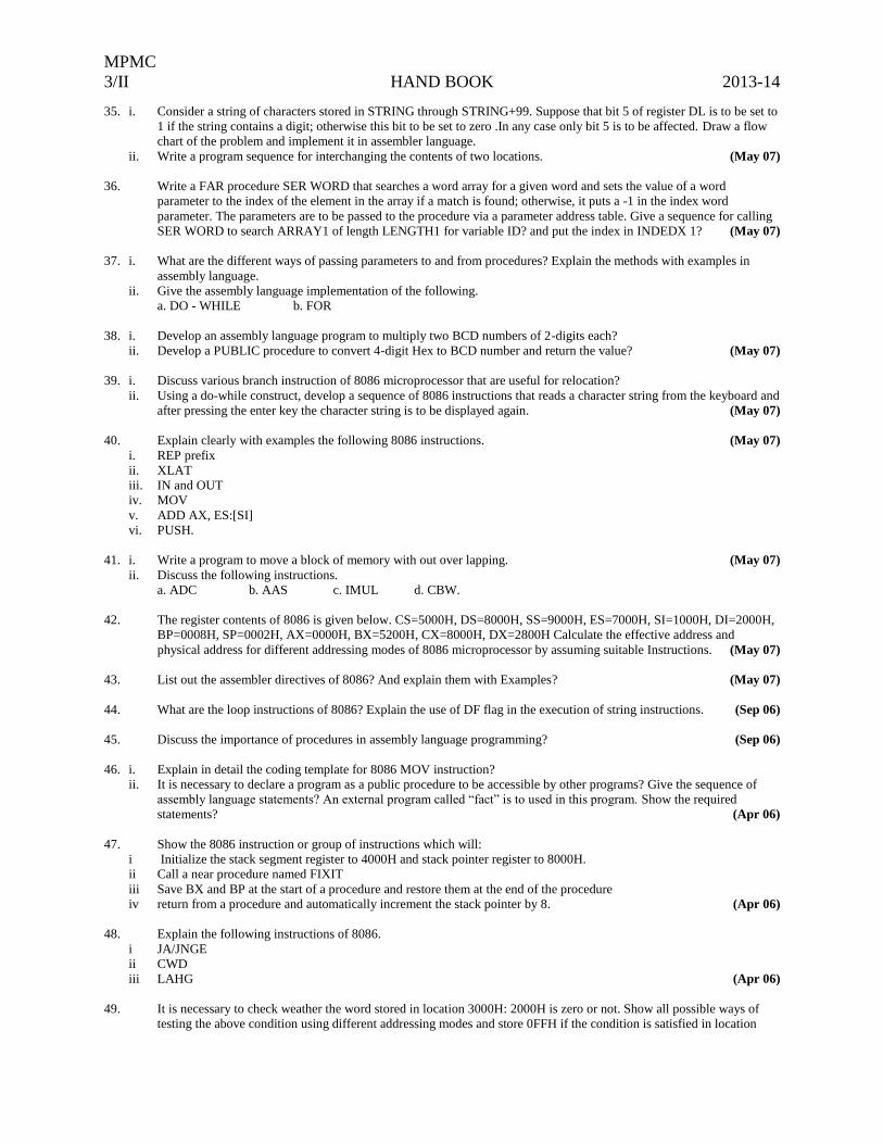
35. i. Consider a string of characters stored in STRING through STRING+99. Suppose that bit 5 of register DL is to be set to
1 if the string contains a digit; otherwise this bit to be set to zero .In any case only bit 5 is to be affected. Draw a flow
chart of the problem and implement it in assembler language.
ii. Write a program sequence for interchanging the contents of two locations. (May 07)
36. Write a FAR procedure SER WORD that searches a word array for a given word and sets the value of a word
parameter to the index of the element in the array if a match is found; otherwise, it puts a -1 in the index word
parameter. The parameters are to be passed to the procedure via a parameter address table. Give a sequence for calling
SER WORD to search ARRAY1 of length LENGTH1 for variable ID? and put the index in INDEDX 1? (May 07)
37. i. What are the different ways of passing parameters to and from procedures? Explain the methods with examples in
assembly language.
ii. Give the assembly language implementation of the following.
a. DO - WHILE b. FOR
38. i. Develop an assembly language program to multiply two BCD numbers of 2-digits each?
ii. Develop a PUBLIC procedure to convert 4-digit Hex to BCD number and return the value? (May 07)
39. i. Discuss various branch instruction of 8086 microprocessor that are useful for relocation?
ii. Using a do-while construct, develop a sequence of 8086 instructions that reads a character string from the keyboard and
after pressing the enter key the character string is to be displayed again. (May 07)
40. Explain clearly with examples the following 8086 instructions. (May 07)
i. REP prefix
ii. XLAT
iii. IN and OUT
iv. MOV
v. ADD AX, ES:[SI]
vi. PUSH.
41. i. Write a program to move a block of memory with out over lapping. (May 07)
ii. Discuss the following instructions.
a. ADC b. AAS c. IMUL d. CBW.
42. The register contents of 8086 is given below. CS=5000H, DS=8000H, SS=9000H, ES=7000H, SI=1000H, DI=2000H,
BP=0008H, SP=0002H, AX=0000H, BX=5200H, CX=8000H, DX=2800H Calculate the effective address and
physical address for different addressing modes of 8086 microprocessor by assuming suitable Instructions. (May 07)
43. List out the assembler directives of 8086? And explain them with Examples? (May 07)
44. What are the loop instructions of 8086? Explain the use of DF flag in the execution of string instructions. (Sep 06)
45. Discuss the importance of procedures in assembly language programming? (Sep 06)
46. i. Explain in detail the coding template for 8086 MOV instruction?
ii. It is necessary to declare a program as a public procedure to be accessible by other programs? Give the sequence of
assembly language statements? An external program called “fact” is to used in this program. Show the required
statements? (Apr 06)
47. Show the 8086 instruction or group of instructions which will:
i Initialize the stack segment register to 4000H and stack pointer register to 8000H.
ii Call a near procedure named FIXIT
iii Save BX and BP at the start of a procedure and restore them at the end of the procedure
iv return from a procedure and automatically increment the stack pointer by 8. (Apr 06)
48. Explain the following instructions of 8086.
i JA/JNGE
ii CWD
iii LAHG (Apr 06)
49. It is necessary to check weather the word stored in location 3000H: 2000H is zero or not. Show all possible ways of
testing the above condition using different addressing modes and store 0FFH if the condition is satisfied in location
MPMC
3/II HAND BOOK 2013-14
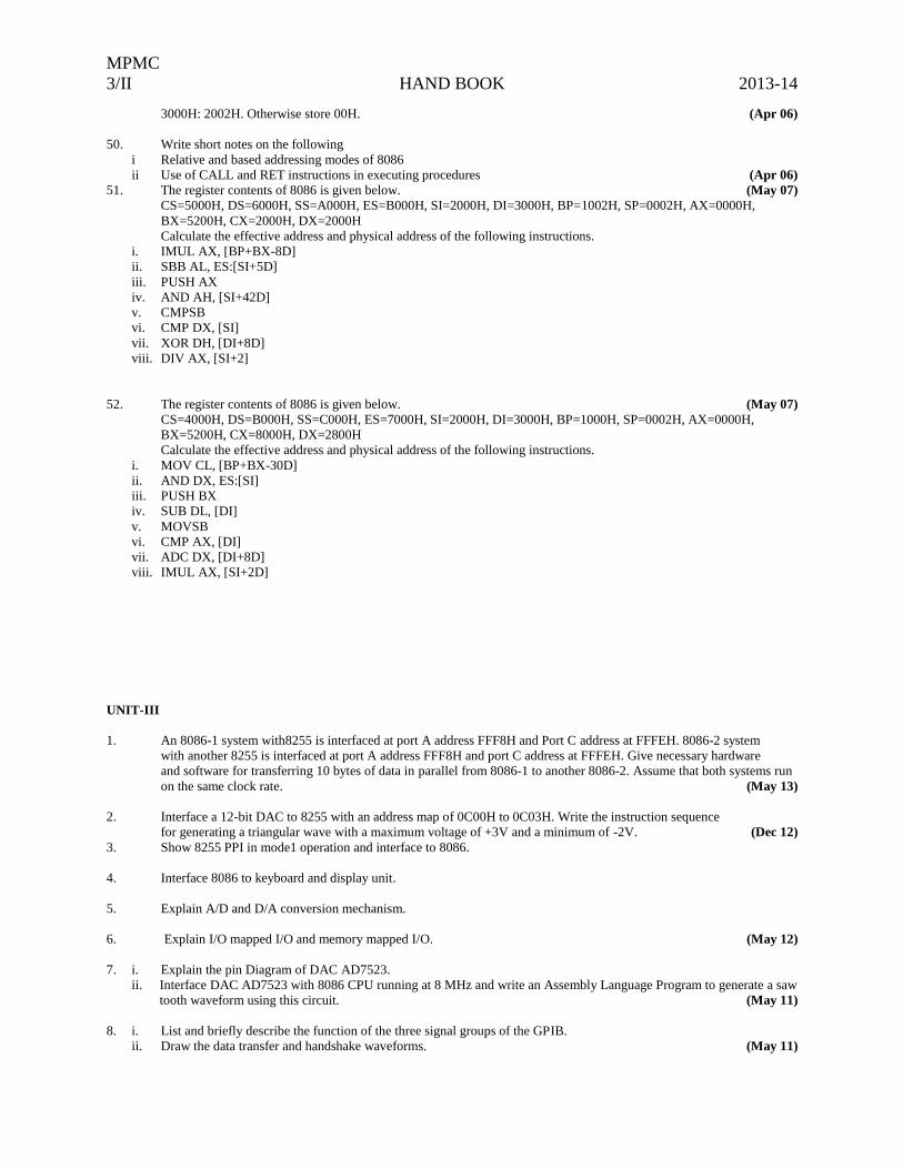
3000H: 2002H. Otherwise store 00H. (Apr 06)
50. Write short notes on the following
i Relative and based addressing modes of 8086
ii Use of CALL and RET instructions in executing procedures (Apr 06)
51. The register contents of 8086 is given below. (May 07)
CS=5000H, DS=6000H, SS=A000H, ES=B000H, SI=2000H, DI=3000H, BP=1002H, SP=0002H, AX=0000H,
BX=5200H, CX=2000H, DX=2000H
Calculate the effective address and physical address of the following instructions.
i. IMUL AX, [BP+BX-8D]
ii. SBB AL, ES:[SI+5D]
iii. PUSH AX
iv. AND AH, [SI+42D]
v. CMPSB
vi. CMP DX, [SI]
vii. XOR DH, [DI+8D]
viii. DIV AX, [SI+2]
52. The register contents of 8086 is given below. (May 07)
CS=4000H, DS=B000H, SS=C000H, ES=7000H, SI=2000H, DI=3000H, BP=1000H, SP=0002H, AX=0000H,
BX=5200H, CX=8000H, DX=2800H
Calculate the effective address and physical address of the following instructions.
i. MOV CL, [BP+BX-30D]
ii. AND DX, ES:[SI]
iii. PUSH BX
iv. SUB DL, [DI]
v. MOVSB
vi. CMP AX, [DI]
vii. ADC DX, [DI+8D]
viii. IMUL AX, [SI+2D]
UNIT-III
1. An 8086-1 system with8255 is interfaced at port A address FFF8H and Port C address at FFFEH. 8086-2 system
with another 8255 is interfaced at port A address FFF8H and port C address at FFFEH. Give necessary hardware
and software for transferring 10 bytes of data in parallel from 8086-1 to another 8086-2. Assume that both systems run
on the same clock rate. (May 13)
2. Interface a 12-bit DAC to 8255 with an address map of 0C00H to 0C03H. Write the instruction sequence
for generating a triangular wave with a maximum voltage of +3V and a minimum of -2V. (Dec 12)
3. Show 8255 PPI in mode1 operation and interface to 8086. (May 12)
4. Interface 8086 to keyboard and display unit. (May 12)
5. Explain A/D and D/A conversion mechanism. (May 12)
6. Explain I/O mapped I/O and memory mapped I/O. (May 12)
7. i. Explain the pin Diagram of DAC AD7523.
ii. Interface DAC AD7523 with 8086 CPU running at 8 MHz and write an Assembly Language Program to generate a saw
tooth waveform using this circuit. (May 11)
8. i. List and briefly describe the function of the three signal groups of the GPIB.
ii. Draw the data transfer and handshake waveforms. (May 11)
MPMC
3/II HAND BOOK 2013-14
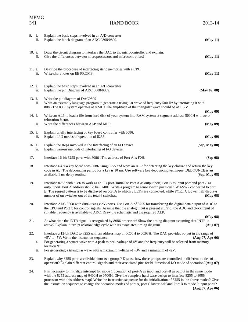
9. i. Explain the basic steps involved in an A/D converter
ii. Explain the block diagram of an ADC 0808/0809. (May 11)
10. i. Draw the circuit diagram to interface the DAC to the microcontroller and explain.
ii. Give the differences between microprocessors and microcontrollers? (May 11)
11. i. Describe the procedure of interfacing static memories with a CPU.
ii. Write short notes on EE PROMS. (May 11)
12. i. Explain the basic steps involved in an A/D converter
ii. Explain the pin Diagram of ADC 0808/0809. (May 09, 08)
13. i. Write the pin diagram of DAC0800
ii. Write an assembly language program to generate a triangular wave of frequency 500 Hz by interfacing it with
8086.The 8086 system operates at 8 MHz The amplitude of the triangular wave should be at + 5 V.
(May 09) 14. i. Write an ALP to load a file from hard disk of your system into RAM system at segment address 5000H with zero
relocation factor.
ii. Write the differences between ALP and MLP. (May 09)
15. i. Explain briefly interfacing of key board controller with 8086.
ii. Explain I / O modes of operation of 8255. (May 09)
16. i. Explain the steps involved in the Interfacing of an I/O device. (Sep, May 08)
ii. Explain various methods of interfacing of I/O devices.
17. Interface 16-bit 8255 ports with 8086 . The address of Port A is F0H. (Sep 08)
18. Interface a 4 x 4 key board with 8086 using 8255 and write an ALP for detecting the key closure and return the key
code in AL. The debouncing period for a key is 10 ms. Use software key debouncing technique. DEBOUNCE is an
available 1 ms delay routine. (Sep, May 08)
19. Interface 8255 with 8086 to work as an I/O port. Initialize Port A as output port, Port B as input port and port C as
output port. Port A address should be 0740H. Write a program to sense switch positions SW0-SW7 connected to port
B. The sensed pattern is to be displayed on port A to which 8 LEDs are connected, while PORT C Lower half displays
number of on switches out of the total 8 switches. (May 08)
20. Interface ADC 0808 with 8086 using 8255 ports. Use Port A of 8255 for transferring the digital data output of ADC to
the CPU and Port C for control signals. Assume that the analog input is present at I/P of the ADC and clock input of
suitable frequency is available to ADC. Draw the schematic and the required ALP.
(May 08) 21. At what time the INTR signal is recognized by 8086 processor? Show the timing diagram assuming that INTR is
active? Explain interrupt acknowledge cycle with its associated timing diagram. (Aug 07)
22. Interface a 12-bit DAC to 8255 with an address map of 0C00H to 0C03H. The DAC provides output in the range of
+5V to -5V. Write the instruction sequence. (Aug 07, Apr 06)
i. For generating a square wave with a peak to peak voltage of 4V and the frequency will be selected from memory
location ‘F’.
ii. For generating a triangular wave with a maximum voltage of +3V and a minimum of -2V.
23. Explain why 8255 ports are divided into two groups? Discuss how these groups are controlled in different modes of
operation? Explain different control signals and their associated pins for bi-directional I/O mode of operation? (Aug 07)
24. It is necessary to initialize interrupt for mode 1 operation of port-A as input and port-B as output in the same mode
with the 8255 address map of 0400H to 0700H. Give the complete hard ware design to interface 8255 to 8086
processor with this address map? Write the instruction sequence for the initialization of 8255 in the above modes? Give
the instruction sequence to change the operation modes of port A, port C lower-half and Port B to mode 0 input ports?
(Aug 07, Apr 06)
MPMC
3/II HAND BOOK 2013-14
25. Interface an 8-bit DAC to 8255 with an address map of 0100H to 0103H. The DAC provides output in the range of
+5V to -5V. Write the instruction sequence for the following? (May 07)
i. For generating a square wave with a peak to peak voltage of 2V and the frequency will be selected from memory
location ‘FREQ’.
ii. For generating a triangular wave with a maximum voltage of +4V and a minimum of -2V.
26. i. What is BSR mode operation? How it is useful in controlling the interrupt initiated data transfer for mode 1 and 2?
(May 07, Sep 06) ii. Explain the transistor buffer circuit used to drive 7-segment LEDs?
27. Draw the block diagram of 8255 and explain each block? (May 07)
28. Why do we prefer interrupt driven data transfer than programmed I/O transfer? Show the complete hardware design to
resolve the multiple interrupts based on priority? (May 07)
29. The I/O circuitry in an 8086 based system consists of five I/O devices with one status signal for each device. Design
the required hardware providing two address locations to each device, one for status and other for data. In the range
0F00H to 0FOFH. Write an instruction sequence to test the status of each device and store it. (May 07)
30. i. Write an algorithm and assembly program to convert a 16 bit number to a maximum of 5 unpacked digits.
ii. Write an algorithm and assembly program to convert an unpacked 4 digit BCD number to Binary number.
(May 07) 31. Develop an 8086 assembly language program that reads a key from the keyboard and converts it to uppercase before
displaying it. The program need to terminate, on typing the control C key. (May 07)
32. Write the necessary instruction sequence to initialize 8255 with address 0C00H to 0C03H for the following
combinations.
i. Port A as input port in mode 1 and port B as input port in mode 1 without the interrupt driven i/o.
ii. Port A in mode 2 as output port and port B as input port in mode 0 with interrupt driven i/o.
iii. Port A in mode 0, port c upper half as input ports and port B as input port in mode 1 with interrupt driven i/o.
iv Port A as output port in mode 1 with active interrupt, port B as input port in mode 0 and port C lower half as output
port in mode 0. (Sep 06)
33. Write the necessary instruction sequence to initialize 8255 with address 0400H to 0700H for the following
combinations.
i. Port A in mode 2 and port B as input port in mode 0 without the interrupt driven i/o.
ii. Port A in mode 2 and port B as input port in mode 1 with interrupt driven i/o.
iii. Port A in mode 0, port c upper half as input ports and port B as input port in mode 1 with interrupt driven i/o.
iv. Port A as output port in mode 1 with active interrupt, port B as input port in mode 0 and port C lower half as output
port in mode 0. (Sep, Apr 06)
34. i. Draw the block diagram of 8255 and explain each block?
ii. What is BSR mode operation? How it is useful in controlling the interrupt initiated data transfer for mode 1 and 2?
(Sep 06)
35. Explain why 8255 ports are divided into two groups? Discuss how these groups are controlled in different modes of
operation? Explain different control signals and their associated pins for bi-directional I/O mode of operation?
(Apr 06, Nov 04)
36. An 8086 system with 8255 interfaced at port A address F0H, as a block of 100 data bytes Stored in it. Another 8086
system with another 8255 interface at port A address 80H has another block of 100data bytes stored in it. Interchange
this blocks of data bytes between the two 8086 systems. Draw the necessary hardware scheme and write the necessary
sequence of instructions. Both systems run on the same clock rate. (Apr 05)
37. i. A DAC is interfaced to 8255 with an address map of 0800H to 0803H. Give the hardware design? It is necessary to
design a counter type ADC with the same 8255 and DAC using a comparator. Give the necessary hardware? Provide
the necessary instruction sequence to store a sample in location sample one?
ii. Using the above hardware write the instruction sequence for successive approximation ADC? (Apr 05)
38. Interface a stepper motor with 8-step input sequence to 8086 based system and write the instruction sequence to move
the stepper motor 20 steps in clockwise and 12 steps in anti-clockwise direction. (Apr 05)
MPMC
3/II HAND BOOK 2013-14
39. i. A DAC is interfaced to 8255 with an address map of 0B00H to 0B03H. It is necessary to design an ADC with the same
8255 and DAC using a comparator. Give the necessary hardware?
ii. Using the above hardware write the instruction sequence for successive approximation ADC and counter type ADC?
(Apr 05)
40. Explain how to interface a stepper motor with 4-step input sequence to 8086 based system with the help of hard ware
design? Write the instruction sequence to move the stepper motor 10 steps in clockwise and 12 steps in anti-clockwise
direction. (Apr 05)
41. i. Explain control word format of 8255 in I/O and BSR mode.
ii. Interface 16 bit 8255 ports with 8086. The address of port A if F0H (Nov 04)
43. Design an interfacing circuit to setup 8255 in the hand shake mode and write the instructions to transfer data under
status check I/O and Interrupt I/O (Nov 02)
44. Give the relevant hardware and software for interfacing a Stepper Motor to 8086 based system. (Nov 02)
45. What is a stepper motor? Give the schematic for interfacing of stepper motor to 8086 processor and an ALP to control
the direction and speed of the stepper motor. (Nov 02)
UNIT-IV
1. i) Explain how to interface D/A converter to 8086 processor. Give the hardware and software for it.
ii) Explain type 3 interrupt in 8086. (May 13)
2. Explain the difference between maskable and non maskable interrupts with examples. Discuss
about the interrupt priorities of 8259 controller (Dec 12)
3. Explain the interface of 8257 to 8086. (May 12)
4. Explain 8259 interrupt controller along with control registers. (May 12)
5. Explain interrupt service routine concept. (May 12)
6. Explain the interrupt structure of 8086 (May 12)
7. i. With a neat sketch explain 8237 DMA controller and its operation? (May 11)
ii. With the help of basic cell explain SRAM and DRAM?
8. i. Discuss the following modes of DMA transfer
a. Signal transfer
b. Block transfer (May 11)
9. i. Write an 8086 assembler program to decide the parity of a given number. The given number multiple be a multi byte
might with a maximum length of 8 bytes.
ii. Write a short notes on assembler. (May 11)
10. i. Describe the control structure for looping and for decision blocks.
ii. Explain passing the parameters onto stack space in a routine. (May 11)
11. i. Explain the priorities of DMA requests
ii. Explain the interfacing of 8257 with 8086. (May 11, May 08)
12. i. Explain pin diagram of 8259 PIC
ii. Explain the interrupt sequence in 8086 system. (May 09, Sep 08)
13. i. Describe the procedure of interfacing static memories with a CPU.
MPMC
3/II HAND BOOK 2013-14
ii. Write a short notes on EE PROMS. (May 09)
14. i. Explain the bus structure of 8086 system. (May 09, 08)
ii. Explain the differences between memory and I/O interfacing.
15. i. Draw and discuss the status register of 8257?
ii. Discuss the priorities of DMA request inputs of 8257? (May 09)
16. Explain various operating modes of 8259 PIC. (Sep 08)
17. i. What are the registers available in 8257? What are their functions (Sep 08, Aug 07)
ii. Explain the functions of following signals of 8257
a. HLDA
b. AEN
c. MARK
d. MEMR.
18. Interface DMA controller 8257 with 8086 so that the channel 0 DMA address register has an I/O address 80 H and the
mode set register has an address 88H. Initialize 8257 with a normal priority, TC stop and non extended write. Auto
load is not required . Write an ALP to move 2 KB of data from a peripheral device to memory address 2000:5000H
with the above initialization. (Sep 08)
19. i. Explain the bus structure of 8086 system. (May 08)
ii. Explain the fundamental concepts of DRAM controller.
20. i. Explain the Static Ram interfacing. (May 08)
ii. Interface TWO 4KX8 EPROMS and two 4K X 8 RAM chips with 8086. Select suitable memory map.
21. What are the functions of a DMA controller? Explain the various DMA modes. Describe in brief the steps that take
place during a DMA Operation. (Aug 07)
22. i. What is the purpose of ALE, BHE, DT/R and DEN pins of 8086? Show their timing in the system bus cycle of 8086?
ii. Write an 8086 ALP to multiply two 8-bit numbers using SHIFT and ADD method. Store the result in DX register.(Aug, May 07)
23. i. What are the contents of the data bus and the status of A0 and BHE when the following instructions are executed in
8086? (Aug 07)
a CPU writes a byte 11 H at memory location 1000H : 0002 H.
b. CPU writes a word 2211 H at memory location 1000H : 0003 H.
ii. Write the functions of the following pins of 8086.
a. MN/ MX b. DEN c. ALE d. Ready.
iii. Draw a block diagram to interface two 16K X 8 SRAM (62128) to the 16-bit data bus of 8086 based system. Design
the address decoder for the address range from 00000H - 07FFFFH for both the SRAMs.
24. i. Which interrupt type is associated with NMI? Mention its vector address.
ii. What is the purpose of IF flag in handling the interrupts?
iii. Which interrupt type is associated with TF flag? What is the vector address? Explain the use of this interrupt.(Aug, May 07)
25. i. Describe the interrupt acknowledge cycle with suitable timing diagram. (Aug 07)
ii. Which interrupt type is associated with TF flag? What is its vector address?
iii. What is meant by vector address? How the vector address is used to service the interrupts?
26. i. Write an instruction sequence that will cause the priority of an 8259, whose even address is 0800H, to be IR5, IR6,
IR7, IR0, IR1, IR2, IR3, IR4. Solve this problem when the current priority is IR1 and for the second time assuming the
current priority to be IR7.
ii. Explain with examples how interrupt type-1 and type-3 provide debugging feature. (Aug 07)
27. Explain the following modes of operation of 8259. (Aug 07)
i. Fully nested mode
ii. Rotating priority mode
iii. Special masked mode, and
iv. Polled mode
MPMC
3/II HAND BOOK 2013-14
28. i. Discuss the sequence of operations performed in the interrupt acknowledge cycle? (Aug 07)
ii. What is the purpose of IF flag in handling the interrupts?
iii. Which interrupt type is associated with TF flag? What is the vector address Explain the use of this interrupt?
29. i. What is the purpose of operational command words of 8259? Explain their format and the use? (Aug 07)
ii. What is type 2 interrupt? Explain the condition for initiating type 2 interrupt? What is the priority of this interrupt in
8086?
30. i. What is the address map of interrupt address vector table? (Aug 07)
ii. Give the priority of 8086 interrupts, hardware and software? Explain why single step interrupt is having lower priority?
31. i. Draw the block diagram of 8259 and explain each block? Discuss the salient features of 8259?
ii. What is the address map of interrupt address vector table? How many interrupts that this table can serve?
(Aug, May 07) 32. i. What is the purpose of operational command words of 8259? Explain their format and the use. (May 07)
ii. Draw and explain the interrupt acknowledge cycle of 8086.
33. i. Describe the response that an 8259 will make if it receives an interrupt signal on its IR3 and IR5 inputs at the same
time. Assume fixed priority for the IR inputs. What response will the 8259 make if it is servicing an IR5 interrupt, and
an IR3 interrupt signal occurs. (May 07)
ii. Show the sequence of command words and instructions that you would use to initialize an 8259 with a base address of
FF10H as follows: Edge triggered; Only one 8259; 8086 system; Interrupt Type-40 corresponds to IR0 input; Normal
EOI; Non-buffered mode; Not special fully nested mode; IR1 and IR3 unmasked.
34. i. Four sources are connected to IR lines of 8259. Emergency signal, Keyboard, A/D converter and Printer, of these,
emergency signal has highest priority and the printer has lowest priority. Write all the initialization instructions. (May 07)
ii. Write initialization instructions of 8259 PIC to meet the following specifications:
a. Interrupt vector address: 2090 H
b. Call address interval of 8 bytes
c. Nested mode.
35. i. Explain the interrupt structure of 8259. (May 07)
ii. Explain the operating modes of 8259.
36. i. Design a memory interface in an 8088 based system with 64KB SRAM and 16KB EPROM. The SRAM starts at
00000H address and EPROM ends at FFFFFH. All the memory chips are of size 16KB. Use 74LS138 decoder.
ii. With the help of basic cell explain SRAM and DRAM? Discuss the advantages and disadvantages of the above
memories? (May 07)
37. i. With a neat sketch explain 8237 DMA controller and its operation? (May 07)
ii. With the help of basic cell explain SRAM and DRAM?
38. i. How DRAM’s are different from SRAM’s? Why DRAMs are said to employ address multiplexing?
ii. What are the conditions that will cause EU to enter a ‘Wait State’? (May 07)
iii. What logic levels would you find on BHE and A0:
a. When an 8086 is writing a byte to the memory address 04032H,
b. When it is writing a word to the memory address 04032H. Also, describe the 8086 bus operations required to write a
word at memory address 04031h.
39. i. List the signals in minimum and maximum modes. (May 07)
ii. Explain the roles of pins TEST, LOCK.
iii. Which are the pins of 8086 that are to be connected to interface 8284 and explain their functions?
40. Write an initialization sequence for an 8259 that is the only 8259 in an 8086 based system, with an even address of
0F0H that will cause.
i. Request to the edge triggered mode
ii. IR0 request to an interrupt type 30
iii. SP/EN to output a disable signal to the data-bus transceivers.
iv. The ISR bits to be cleared automatically at the end of second INTA pulse.
v. The IMR to be cleared.
vi The highest priority interrupt will be IR6. (Sep 06)
MPMC
3/II HAND BOOK 2013-14
UNIT-V
1. a) Draw and explain interrupt acknowledgement cycle of 8086.
b) Explain the mode word format and the command word format of 8251A. (May 13)
2. a) Briefly discuss about the serial communication standards
b) Describe the functions of the DSR,DTR,RTS,CTS,TXD, and RXD signals exchanged between a terminal and a
modem. (Dec 12)
3. Explain the need for RS232C interface. Explain serial communication standards with respect to voltage levels. (May 12)
4. Explain 8251 USART. (May 12)
5. Explain the interfacing of RS-232 to 8086. (May 12)
6. Explain IEEE-488 bus and its protocols. (May 12)
7. i. Explain the pin structure of RS232C and also discuss about voltage and current specifications of RS 232C.
ii. Describe important features of 8251 USART. (May 11, Sep 08)
8. i. Explain digital transmission using modems?
ii. Explain the following pins of 8251.
a. TxRDY
b. DSR
c. SYNDET/BD
d. RTS (May 11, May 09)
9. i. Write the sequence of events for 8251 initialization with necessary 8086 instructions.
ii. Draw and explain the block diagram of 8251. (May 11, May 09)
10. i. Explain with a neat diagram the working of 8251 PCI. (May 09)
ii. Draw the interface circuits for data conversion from
a. TTL to RS232C and
b. RS232C to TTL
11. i. Draw the internal block diagram of 8251 and explain about each block in detail. (May 09, May 08)
ii. Distinguish between Synchronous and Asynchronous data formats.
12. i. Give the specifications of RS232C? (Sep 08)
ii. Explain about line driver and line receiver used in serial communication?
iii. Give the status register of 8251 and explain each bit.
13. i. Explain why serial data transfer is mostly preferred over parallel data transfer. Give reasons. (Sep 08)
ii. Distinguish between data formats used for Synchronous and Asynchronous serial data transfer modes.
14. i. Write an 8086 instruction sequence for transmitting the characters using 8251 on a polled basis.
ii. Write an 8086 instruction sequence for receiving 100 characters using 8251 on a polled basis and store them in
memory at location 2050H. (Sep 08)
15. i. Write an 8086 instruction sequence for transmitting 50 characters which are stored from the location 2010H using
8251. (May 08)
ii. Write an 8086 instruction sequence for receiving 50 characters using 8251 and store them in memory at location
2080H.
16. i. Describe the bit assignment for mode instruction format of 8251 for both Synchronous and Asynchronous modes.(May 08)
ii. Write an instruction sequence for initializing 8251 for the following combination.
a. Asynchronous mode
b. Even parity
c. 7 data bits

MPMC
3/II HAND BOOK 2013-14
d. 2 stop bits
e. 6400 baud rate
17. Interface a 12-bit DAC to 8255 with an address map of 0800 H to 0803 H. The DAC provides output in the range of
+5V to -5V. Write the instruction sequence.
i. For generating a square wave with a peak to peak voltage of 2V and the frequency will be selected from memory
location “FREQ”.
ii. For generating a triangular wave with a maximum voltage of +5V and a minimum of 0V. (Aug 07)
18. i. What is the difference between 20mA current loop and RS232-C standard? (Aug, May 07)
ii. Explain the necessity of RS232 to TTL interface and draw the circuit?
iii. Draw the circuit of TTL to RS232 and explain the necessity of this interface.
19. i. What do you mean by high-speed serial communication standard? When the high-speed serial communication
standards are used?
ii. A terminal is transmitting asynchronous serial data at 9600 baud. What is the bit time? Assuming 6 data bits, odd
parity, and 2 stop bits. How long does it take to transmit one character? (Aug 07)
20. i. Explain the operation of 8251 in Synchronous mode of communication. (Aug 07)
ii. Write short note on RS-232C standard.
21. i. Explain the features of 8251 clearly. (Aug 07)
ii. Explain clearly the operation of receiver section of 8251.
22. i. What are the MODEM standards? Explain why a MODEM is required to send digital data over standard telephone-
lines.
ii. Show the bit pattern for the mode word and the command word that must be sent to an 8251 to initialize the device as
follows: Baud rate factor of 16, 5-bits per character, odd parity, 1 1/2 stop bits, transmit interrupt enabled, DTR and
RTS asserted, Error flags reset, send break character. (Aug 07)
23. i. With a neat sketch explain the internal organization of SRAM chip? List out the input and output pins? Discuss their
function in a system?
ii. Draw the basic cell structure of EPROM and explain the principle of operation?
iii. Distinguish between EPROM and E2PROM? Mention their application areas? (Aug 07)
24. It is necessary to interface 128KB SRAM and 32KB EPROM to an 8086 based system. The size of SRAM and
EPROM chips is 16KB. Address map of SRAM is fixed from 00000H to 1FFFFH and that of EPROM is from F8000H
to FFFFFH. Design the entire memory interface? Give the address map of individual chip?
(Aug 07) 25. A target system based on 8086 processor uses less amount of SRAM. The programs are stored in EPROM that starts
from 80000H ends with the address of FFFFFH. The capacity of SRAM is 16KB interfaced at address 00000H. The
chip size is 8KB. The size of EPROM is 64KB. Show the complete memory interface?
(Aug 07) 26. i. Draw and explain Command and Mode word formats of 8251. (May 07)
ii. Explain the interfacing of 8251 with 8086 in memory mapped I/O mode.
27. i. Draw and explain the synchronous mode transmit and receive data formats of 8251. (May 07)
ii. Write a program to initialize 8251 in synchronous mode with even parity, single SYNC character, 7-bit data character.
Then receive FFH bytes of data from a remote terminal and store it in the memory at address 5000H:2000H.
28. i. Explain the operation of 8251 in Asynchronous mode of communication. (May 07)
ii. How TTL to RS-232C and RS-232C to TTL conversions are achieved?
29. i. Distinguish between synchronous and asynchronous serial data transmission techniques? Discuss the advantages and
disadvantages?
ii. Draw the block diagram of combination of FAX and Data Modem? Explain each block? (May 07, Nov 04)
30. i. With a neat sketch explain 8237 DMA controller and its operation? (May 07, 06)
MPMC
3/II HAND BOOK 2013-14
ii. How do we connect RS-232C equipment
a. To data terminal type devices?
b. To serial port of SDK ?86, RS-232C connection?
31. i. Explain the methods for excitation of stepper motor. (May 07)
ii. Interface stepper motor with 8086 microprocessor system and write an assembly language program to rotate it by 1800.(May 07)
32. i. Interface a 4x4 keyboard using two 8255 ports and write a program to read the code of a pressed key.
ii. Show the sequence of instructions you can send to the 8279 of the SDK-86 board to display 8888.
(May 07) 33. i. Write an initialization sequence to operate 8251 in asynchronous mode with 8-bit character size, baud rate factor 64,
two stop bits and odd parity enable. The 8251 is interfaced with 8086 at address 082H.
ii. Write the instruction sequence to re-initialize the above 8251 in synchronous mode with even parity, single SYNC
character and 8-bit character size? (Apr 06, 05)
34. i. Discuss Overrun error and Framing error with reference to 8251?
ii. Discuss the mode instruction format of 8251 for synchronous and asynchronous mode of operation?
iii. Explain single transfer mode and block transfer mode of 8237? (Apr 06)
35. i. How do we connect RS-232C equipment
a. To data terminal type devices?
b. To serial port of SDK -86, RS-232C connection?
ii. Give the specifications of RS-232C. (Apr 06)
UNIT-VI
1. a) Assume that ROM space of 8051 starting at 250H contains “Hello”, write a program to transfer the bytes into RAM
location starting at 40H.
b) Explain the operation in 8051 microcontroller and also discuss necessary instructions to access the stack. (May 13)
2. a) Explain the organization of memory in 8051 controller.
b) Explain the structures of program status word register of 8051. (Dec 12)
3. Give any five instructions of 8051 and explain each. (May 12)
4.. Explain internal and external memory of 8051. (May 12)
5. Explain the timers in 8051 and its modes. (May 12)
6. What is the difference between microprocessor and microcontroller? Give 8051 architecture (May 12)
7. i. Draw the oscillator circuit and also draw the 8051 timing diagram.
ii. Discuss in detail about parallel I/O ports in 8051 micro controller and explain how these ports are accessible for
specific applications. (May 11, May 09, Sep 08)
8. i. Explain the interfacing of external data memory to 8051 using 74LS573 latch with a neat diagram and draw the
waveforms.
ii. Draw the pin diagram of 74LS573 latch and explain how you can demultiplex the address and data bus using this latch.
(May 11)
9. i. Explain the functions of Port 0, Port 2 and Port 3.
ii. Draw and discuss the formats and bit definitions of TCON register in 8051 (May 11)
10. i. Discuss the advantages of micro controller based system over micro processer based system.
ii. Enlite the relevent features of 8051 forming of micro controllers. (May 09)
11. Draw and discuss the formats and bit definitions of the following registers in 8051 microcontroller.
i. IP
ii. TMOD
iii. TCON
iv. SCON (May 09)
MPMC
3/II HAND BOOK 2013-14
12. i. Draw and explain the capacities of internal and external Program memory and internal and external data memory?
ii. Define PUSH and POP instructions and give examples. Explain the stack operation. (May 09)
13. i. Draw the architectural diagram of 8051 microcontroller and explain in detail about each block. (Sep 08)
ii. Explain the basic differences between a microprocessor and a microcontroller.
14. i. Give the features of 8051 microctroller. (Sep 08)
ii. Explain the following pins of 8051.
a. AD0 - AD7
b. T0 and T1
c. INT0 and INT1
d. TxD and RxD
15. i. Interface the 7-segment displays in time-multiplexing and display select method and explain the same.
ii. Write a 8051 program to control the operation of a 7-segment displays with time multiplexing and display method.
Assume that the 7-segment codes for the characters to be displayed are at 40,42,44,46H respectively in the internal
RAM. Whereas, the cathode select codes for each of the displays are at 41,43,45,47H respectively. (May 08)
16. Discuss the following signals of 8051 (May 08)
.
i. ALE
ii. T0 and T1
iii. TxD
iv. RxD
17. i. Discuss in detail about 8051 instruction set. (May 08)
ii. Give the comments for the following instructions.
a. MOV @RP , #n
b. MOV A, 80h
c. MOV 0A8h, 77h
d. MOV A, add
e. MOV add, @RP
f. MOV A, @R0
18. i. Explain the arithmetic instructions of 8051 with examples. (May 08)
ii. Write 8051 program to subtract the contents of RAM location 13h from RAM location 2Bh, put the result in RAM
location 3Ch.
19. i. What is the address map of interrupt address vector table? Explain how a vector address is stored in this table? How
many interrupts are serviced with this table? (Apr 07)
ii. What is the purpose of operational command words of 8259? Explain their format and the use?
20. Draw and discuss the formats and bit definitions of the following SFR’s in 8051 microcontroller?
i. PCON
ii. PSW
iii. IP
iv. TMOD (Sep, Apr 06)
21. Discuss the following signal descriptions?
i. ALE/PROG
ii. RXD
iii. TXD (Sep, Apr 06, 05)
22. i. How does 8051 differentiate between the external and internal program memory?
ii. Explain with waveforms different modes of counter/timer in 8051? (Sep, Apr 06)
23. i. Enlist salient features of 8051 family of microcontrollers?
ii. Explain with waveforms different modes of counter/timer in 8051? (Sep 06)
24. Draw and discuss the formats and bit definitions of the following SFR’s in 8051 microcontroller?
MPMC
3/II HAND BOOK 2013-14
i. PSW
ii. IE
iii. SCON
iv. TMOD (Sep, Apr 06, 05)
25. Discuss the following signal descriptions?
i. INT0/INT1
ii. TXD
iii. T0 AND T1
iv. RD (Apr 05)
UNIT-VII
1. a) List out the steps involved in programming the 8051 to transfer data serially.
b). Write an 8051 program to find Y where Y= x2 +5 and x is between 0 and 5. (May 13)
2. a) Explain the timer modes in 8051 controller.
b) Draw the structures of TMOD and TCON registers and explain. (Dec 12)
3. Explain how the interrupts are used in real-time. (May 12)
4. Explain the timers and counters in 8051. (May 12)
5. Explain programming serial communication interrupts. (May 12)
6. Explain special function registers in 8051 and show how they are used for programming. (May 12)
7. i. using a typical 12-bit DAC, generate a step wave form of duration 1 sec, maximum 3 volts and determine the duration
of each step suitably.
ii. Write the pin diagram of DAC 0800. (May 11)
8. Interface 8259 PCI with 8086 at the address 074H. Write an ALP to initialize 8259 in single level triggered mode, with
call address interval of 4, non buffered, no special fully nested mode . Then set the 8259 to operate with IR6 masked,
IR4 as the bottom priority level with special EOI mode. Set the special mask mode of 8259A. Read IRR and ISR in to
registers BH and BL respectively. Let the staring vector address be 0000:0010H. (May 11)
9. i. Describe CPU register structure and internal RAM considerations during programming.
ii What are the registers which serve on an interrupt in 8051. (May 11)
10. i. What are the hardware interrupts’ related to external sources in 8051/52 families?
ii. Explain how do you disable all interrupts during a critical region in a program. (May 11)
11. i. Explain how serial data communication is done with 8051 serial ports.
ii. Explain with waveforms, different modes of serial data transmission modes in 8051. (May 09)
12. i. What is the use of Mode 0 of serial communication in 8051. Write a program to transmit a data 45H in mode0.
ii. What are the various SFRs you need while handling the Timers/Counters. Give the register formats.
(May 09) 13. i. Explain how the timer flag interrupt and the serial port interrupt are generated.
ii. Discuss on external interrupts?
iii. Discuss on interrupt priority? (May 09)
14. i. Write 8051 program to initialize timer 1 in mode 0.
ii. Give the formats of the registers which are used for the counters/timers. (May 09)
15. i. Write 8051 program to generate 2 kHz square waves on pin P1.0 of port 1 using Timer interrupt.
ii. Write 8051 program to receive a serial byte through RxD. (Sep, May 08)
16. i. Give the sequence of events that takes place when the interrupt occurs in 8051. (Sep 08)
MPMC
3/II HAND BOOK 2013-14
ii. Draw the bit formats of IE and IP registers of 8051?
17. i. Discuss in detail about serial port operation in 8051 microcontroller. (Sep 08)
ii. Discuss about various modes of operations of timer in 8051.
18. i. Write 8051 program as an example of interrupt call to a routine, timer 0 is used in mode 0 to overflow and set the timer
0 interrupt flag. When the interrupt is generated, the program vectors to the interrupt routine, resets the timer 0
interrupt flag, stops the timer, and returns. (Sep, May 08)
ii. Discuss the bit format of IP register of 8051?
18. i. Write 8051 program to initialize timer 1 in mode 1. (May 08)
ii. Write 8051 program to generate 2 kHz square waves on pin P1.0 of port 1 using Timer 0 auto reload mode.
19. Give the complete block schematic of an 8051 based system having following specifications: (Aug 07)
i. 64 KB program memory
ii. 64 KB data memory
iii. Make use of 16 K x 8-bit memory chips and 74LS138 decoders.
iv. Indicate clearly the address selected for the memory chips.
20. Draw the port pin circuits of all the ports of 8051 and explain about each port pin circuit clearly. (Aug 07)
21. i. How does 8051 differentiate between the external and internal program memory? (Aug 07)
ii. Explain with waveforms different modes of counter/timer in 8051?
22. Draw and discuss the formats and bit definitions of the following SFR’s in 8051 microcontroller?
i. PCON
ii. PSW
iii. IP
iv. TMOD (Aug 07)
23. Interface two 8255’s to 8051 with starting address of 0F000H? Show the hardware design? Write the instruction
sequence to initialize all ports of first 8255 as output ports in mode 0 and in the second 8255 port A as input in mode 1
and other ports as input in mode 0. (Aug 07)
24. i. Discuss the following signal descriptions? (Aug 07)
a. INT0_INT1
b. TXD
c. T0 AND T1
d. RD
ii. Draw and discuss the formats and bit definitions of the following SFR’s in 8051 microcontroller?
a. TMOD b. PSW
25. Discuss the following signal descriptions? (Aug 07)
i. ALE/PROG
ii. EA/VPP
iii. PSEN
iv. RXD
v. INT0 / INT1
vi. TXD
vii. T0 AND T1
viii. RD
26. i. Enlist salient features of 8051 family of microcontrollers? (Aug 07)
ii. Explain with waveforms different modes of counter/timer in 8051?
27. i. Draw and discuss the formats and bit definitions of the following SFR’s in 8051 microcontroller.
i. PCON ii. PMOD.
ii. Explain the stack organization of 8051 microcontroller. (Aug 07)
28. An 8051 based system requires external memory of four 4Kbytes of SRAM each and two chips of EPROM of size

MPMC
3/II HAND BOOK 2013-14
2Kbytes. The EPROM starts at address 2000H. SRAM address map follows EPROM map. Give the complete memory
interface? (Aug 07)
29. It is necessary to interface 512KB SRAM and 128KB EPROM to an 8086 based system. The size of SRAM and
EPROM chips is 64KB. Address of SRAM starts from 00000H and that of EPROM is from E0000H. Design the entire
memory interface? Give the address map of individual chip? (May 07)
30. i. With a neat sketch explain the function of memory array of PROM? (May 07)
ii. Draw the basic cell structure of EPROM and explain the principle of operation?
iii. Distinguish between EPROM and E2PROM? Mention their application areas?
31. In an SDK-86 kit 64KB SRAM and 32KB EPROM is provided on system and provision for expansion of another
64KB SRAM is given. The on system SRAM address map is from 00000H to 0FFFFH and that of EPROM is from
F8000H to FFFFFH. The expansion slot address map is from 80000H to 8FFFFH. The size of SRAM chip is 32KB.
EPROM chip size is 16KB. Give the complete memory interface and also the address map for individual chips?
(May 07)
UNIT-VIII
1 a) Explain the salient features of AVR RISC controller with reference to its architecture.
b) Discuss the interrupt structure of RISC controller. (May 13)
2 With a neat sketch , explain the architecture of AVR microcontroller. (Dec 12)
3. Explain register file of AVR. (May 12)
4. Explain interrupt structure in AVR. (May 12)
5. Explain memory organization in AVR. (May 12)
6. Explain standard AVR architecture. (May 12)
MPMC
3/II HAND BOOK 2013-14
II GATE QUESTIONS
1.For 8085 microprocessor, the following program is executed
MVI A, 05H;MVIB, 05H;PTR: ADD B;DCR B;JNZ PTR;ADI 03H;HLT;
At the end of program, accumulator contains
(A) 17 H (B) 20 H (C) 23 H (D) 05 H (GATE 2013)
2.An 8085 assembly language program is given below. Assume that the carry flag is initially unset. The content of the
accumulator after the execution of the program is
MVI A,07HRLCMOV B,ARLCRLCADD BRRC
(A) 8CH (B) 64H (C) 23H (D) 15H (GATE 2011)
3.For the 8085 assembly language program given below, the content of the accumulator after the execution of the program is
3000MVIA,45H
3002MOVB,A
3003STC
3004CMC
3005RAR
3006XRAB
(A) 00H (B) 45H
(C) 67H (D) E7H (GATE-2010)
4. In a microprocessor, the service routine for a certain interrupt starts from a fixed location of memory which cannot be
externally set, butthe interrupt can be delayed or rejected Such an interrupt is
(A) non-maskable and non-vectored
(B) maskable and non-vectored
(C) non-maskable and vectored
(D) maskable and vectored (GATE-2009)
5.An 8085 executes the following instructions
2710 LXI H, 30A0 H
2713 DAD H
2414 PCHL
All address and constants are in Hex. Let PC be the contents of the program counter and HL be the contents of the HL register
pair just after executing PCHL. Which of the following statements is correct ?
(A) PC= 2715H
HL= 30A0H
(B)PC= 30A0H
HL= 2715H
(C) PC=6140H
HL= 6140H
(D) PC =6140H
HL =2715H (GATE-2008)
III. IES QUESTIONS
1.The program counter (PC) in a microprocessor:
(a) counts the number of programs being executed by the microprocessor
(b) counts the number of instructions being executed by the microprocessor
(c) counts the number of interrupts handled by the microprocessor
(d) keeps the address of the next instruction to be fetched (IES 2013)
2. An interrupt in which an external device supplies its address and the interrupt request, is called :
(a) poll interrupt
(b) maskable interrupt
(c) non-maskable interrupt
(d) vectored interrupt (IES 2013)

MPMC
3/II HAND BOOK 2013-14
3. Aliasing in the context of programming language refers to multiple variables having the same :
(a) Memory location
(b) value
(c) identifier
(d) none of these (IES 2013)
4. In a microprocessor, the register which holds the address of the next instruction to be fetched is :
(a) accumulator
(b) program counter
(c) stack pointer
(d) instructor register (IES 2013)
5. The stack pointer will be affected by instructions :
1. PUSH PSW
2. CALL ADDR
3. XTHL
4. RST n
(a) 1, 2, 3, and 4
(b) 1, and 3 only
(c) 1, 2,and 4 only
(d) 2, 3 and 4 only (IES 2013)
6. Following is a 16-bit register for 8085 microprocessor:
(a) Stack pointer
(b) Accumulator
(c) Register A
(d) Register C (IES 2012)
7.The address bus of Intel 8085 is 16-bit wide and hence the memory which can be accessed by this address bus is
(a) 2 k bytes
(b) 4 k bytes
(c) 16 k bytes
(d) 64 k bytes (IES 2012)
8. The register which holds the information about the nature of results of arithmetic or logic operations is called as
(a) Accumulator
(b)Condition code register
(c) Flag register
(d) Process status register. (IES 2012)
9. The instruction that exchanges top of stack with HL pair is
(a) XHTL
(b) SPHL
(c) PUSH H
(d) POP L (IES 2012)
10.Which of the following control bits of 8086 flag register is used to put 8086 in single step mode ? (IES 2011)
1. D
F
2. T
F
3. I
F
4. Z
F

MPMC
3/II HAND BOOK 2013-14
11. Three devices P, Q and R have to be connected to an 8085 microprocessor. Device P has the highest priority and device R has
the lowest priority. L1 this context, which of the following is the correct assignment of interrupt inputs? (IES 2008)
(A) P uses TRAP, Q uses RST 5.5 and R uses RST 6.5
(B) P uses RST 5.5, Q uses RST 6.5 and R uses RST 7.5
(C) P uses RST 7.5, Q uses RST 6.5 and R uses RST 5.5
(D) P uses RST 5.5, Q uses RST 6.5 and R uses TRAP
12. The content of the Program Counter of an intel 8085 A microprocessor specifies which one of the following ?
(A) The address of the instruction being executed
(B) The address of the instruction executed earlier
(C) The address of the next instruction to be executed
(D) The number of instructions executed so far (IES 2008)
13. In an Intel 8085 A, what is the content of the Instruction Register (IR)?
(A) Op-code for the instruction being executed
(B) Operand for the instruction being executed
(C) Op-code for the instruction to be executed next
(D) Operand for the instruction to be executed next (IES 2008)
Assignment Questions:
Unit1
1. Explain the functional block diagram of 8085 microprocessor
2. Draw the block diagram of 8086 and explain the functions of GPRs
3. What are the advantages of the memory segmentation. Discuss about various segment registers in 8086
4. Explain the write cycle operation of the microprocessor with a neat timing diagram in maximum mode.
5. Write short notes on flag register of 8086
Unit2
1. Discuss briefly the instruction formats of 8086
2. Explain string instructions supported by 8086 processor?
3. List out the assembler directives of 8086? And explain them with Examples?
4. explain the difference between procedures and macro’s
5. Explain the use of addressing mode? It is necessary to move a byte from location 4000H:2000H to 4000H:2005H. Give all
possible methods using 8086 addressing modes?
6. Give the instruction sequence that compares the first 10 bytes beginning at STRG1with the first ten bytes beginning at STRG 2
and branches to MATCH if they are equal, otherwise continues in sequence?
Unit3
1. Draw the block diagram of 8255 and explain each block.
2. Explain why 8255 ports are divided into two groups? Discuss how these groups are controlled in different modes of operation?
Explain different control signals and their associated pins for bi-directional I/O mode of operation?
3. Explain briefly interfacing of key board controller with 8086.
4. Draw the circuit diagram to interface the DAC to the microcontroller and explain.
5. Explain various methods of interfacing of I/O devices.
Unit4
1. Explain 8259 interrupt controller along with control registers.
2. Explain the interfacing of 8257 with 8086.
3. What are the registers available in 8257? What are their functions?
4. What are the functions of a DMA controller? Explain the various DMA modes. Describe in brief the steps that take place
during a DMA Operation
5. Discuss the sequence of operations performed in the interrupt acknowledge cycle?
Unit5
1. Write short note on RS-232C standard.
2. Draw the internal block diagram of 8251 and explain about each block in detail
3. Explain the operation of 8251 in Synchronous mode of communication.
4. Explain IEEE-488 bus and its protocols.
5. Explain the interfacing of 8251 with 8086 in memory mapped I/O mode
MPMC
3/II HAND BOOK 2013-14
Unit6
1. Draw the architectural diagram of 8051 microcontroller and explain in detail about each block
2. Explain the functions of Port 0, Port 2 and Port 3
3. Discuss the following signal descriptions?
i. INT0/INT1
ii. TXD
iii. T0 AND T1
iv. RD
4. Explain the basic differences between a microprocessor and a microcontroller.
5. Write 8051 program to subtract the contents of RAM location 13h from RAM location 2Bh, put the result in RAM location
3Ch
Unit7
1. Draw the structures of TMOD and TCON registers and explain
2. Write 8051 program to initialize timer 1 in mode 1.
3. Discuss the interrupt structure of 8051? Mention the priority? Explain how least priority is made as highest priority?
4. Write an 8051 program to find Y where Y= x2 +5 and x is between 0 and 5.
5. Explain the stack organization of 8051 microcontroller.
Unit8
1. With a neat sketch, explain the architecture of AVR microcontroller.
2. Discuss the interrupt structure of RISC controller.
3. Explain different data addressing modes in AVR RISC microcontroller.
4. Explain register file of AVR.
5. Explain the ports of AT90S8515 8 bit AVR Microcontroller.