study of tin whisker growth and their mechanical and electrical
TRANSCRIPT
Examensarbete
Study of Tin Whisker Growth and their
Mechanical and Electrical Properties
Moheb Nayeri Hashemzadeh
LITH - IFM - EX - - 05 / 1499 - - SE

Study of Tin Whisker Growth and their
Mechanical and Electrical Properties
IFM, Linkopings Universitet
Moheb Nayeri Hashemzadeh
LITH - IFM - EX - - 05 / 1499 - - SE
Examensarbete: 20 p
Level: D
Supervisor: Dr. Werner Hugel,Dr. Verena KirchnerRobert Bosch GmbH-AE/QMM-S5
Examiner: Prof. Ulf Helmersson,IFM, Linkopings Universitet
Linkoping: September 2005


Department of Physics and Measurement Technology, IFMLinkoping UniversitySE-581 83 Linkoping
September 2005
x x LITH - IFM - EX - - 05 / 1499 - - SE
Study of Tin Whisker Growth and their Mechanical and ElectricalProperties
Moheb Nayeri Hashemzadeh
The phenomenon of spontaneous growth of metallic filaments, known aswhisker growth has been studied. Until now the problem that Sn whiskergrowth could cause in electronics by making shorts has been partially prohib-ited as Pb and Sn have been used together in solders and coating. Regulationsrestricting Pb use in electronics has made the need to understand Sn whiskergrowth more current.It is shown that whiskers are highly resilient towards vibrations and shocks.A Sn whisker is shown to withstand 55 mA.Results show that reflowing of the Sn plated surface does not prevent exten-sive whisker growth. Results show that intermetallic compound growth cannot be the sole reason behind whisker growth. Nickel and silver underlayerhave been shown not to prevent whisker growth, but perhaps restrain whiskergrowth. Heat treatment damped whisker growth considerably. It is judgedthat base material CuSn6 is less prone to show whisker growth than CuSn0.15and E-Cu58.
Tin whiskerNyckelordKeyword
SammanfattningAbstract
ForfattareAuthor
TitelTitle
URL for elektronisk version
ISRN NUMMER:SprakLanguage
Svenska/Swedish
Engelska/English
RapporttypReport category
Licentiatavhandling
Examensarbete
C-uppsats
D-uppsats
Ovrig rapport
Avdelning, InstitutionDivision, Department
DatumDate
Abstract
Purpose
The phenomenon of spontaneous growth of metallic filaments, known as whiskers,has been studied and compared with existing theories. Until now the problem thattin whisker growth could cause in electronics by making shorts has been partiallyprohibited as lead and tin have been used together in solders and coating. Due toa more environment aware society, where use of lead in solder and coating will berestricted, the need of understanding the phenomenon of tin whisker growth hasbecome more current.A study of the mechanical and electrical durability of tin whiskers has also beencarried out.
Procedure
Tin whiskers current carrying capacities was tested and based on the experimentalresults finite element method calculations were made in the Ansys program. Tinwhiskers endurance against vibrations and shocks have been calculated and tested.Whisker growth on different metallic systems, undergoing different conditions havebeen observed. The metallic systems have been three different sorts of base materi-als (all consist mainly of copper) with a layer of dull or bright tin on it and in somecases nickel or silver underlayer between the base material and the tin layer. Thetest conditions the samples underwent with different combinations were: solderingsimulation, temperature cycling between −60 oC to 60 oC, humidity storage, hightemperature storage and room temperature storage. Some samples were also heattreated post plating, for 5 minutes at 180 oC. Some of the samples were studiedwith help of Focused Ion Beam systems.
Nayeri Hashemzadeh, 2005. 6
7
Results and Conclusions
Both calculations and tests showed that whiskers are highly resilient towards vi-brations common in vehicles. Tests showed also that whiskers can withstand veryhigh shocks, not breaking when subjected to shocks of 1000 m/s2 during 6 ms.Tests have shown whiskers withstanding currents up to 55 mA. The longer thewhiskers the lower current carrying ability, while thicker whiskers can carry highercurrents. The whisker that could withstand 55 mA was 120 µm long and had adiameter of 5.5 µm.Due to the shifting quality of the plating of the samples clear conclusions regardingstorage conditions that are favorable for whisker growth can not be made. Thispoints to the importance of process stability when plating, as to get homogenousplating quality.Results show that soldering simulation, which is melting the tin plated surfacedoes not prevent extensive whisker growth. Results show that intermetallic com-pound growth can not be the sole reason for whisker growth. Nickel and silverunderlayer have been shown not to prevent whisker growth, but perhaps restrainit. Heat treatment damped whisker growth considerably but did not prevent it.It is judged that base material CuSn6 is less prone to show whisker growth thanCuSn0.15 and E-Cu58.
Keywords: Tin whisker
Acknowledgements
I would like to thank Prof. Ulf Helmersson for his help and support, making itpossible for me to do my master thesis in Germany at Robert Bosch GmbH, Reut-lingen.
I would like to thank both my supervisors at Robert Bosch GmbH, Dr. WernerHugel and Dr. Verena Kirchner, for the help and the support I have received withmy work. Dr. Werner Hugel had a great part in helping me in my work, fromhaving ordered the samples that were studied during this work, to booking testsessions as well as helping with the theoretical part of the work. Dr. Verena Kirch-ner was very helpful in helping with practical issues and giving advise in theoreticalmatters as well as helping me write this report.I would also like to thank all the other people at Robert Bosch GmbH that werevery forthcoming in helping me, specially following names come to mind, eventhough there were many more:Joachim Gugeler for the tests concerning mechanical durability.Thomas von Bargen for the FEM simulations.Markus Schill for the FIB sessions.Sukru Tavasligolu for saving my computer several times.Markus Guber for providing time to discuss his results and views regarding whiskergrowth.Fabian Bez for helping me looking through some of the samplesPravin Sinha for helping me in searching for articles.David Nerz for his help with some of the samples.Nathalie Becker for her help in practical and scientific matters.Parviz Kamvar for his advices in scientific matters.
Moreover I would like to thank my brother Mohit Nayeri, for being supportiveboth on a scientific sense as well as on a personal level.
I would like to dedicate this work to my mother, Mary Berari.
Nayeri Hashemzadeh, 2005. 8

Frequently Used Abbreviationsand Symbols
EDX Energy Dispersive X-ray spectroscopeFEM Finite Element MethodFIB Focused Ion BeamIMC Intermetallic CompoundLM Light MicroscopePSD Power Spectral DensityRoHS Restriction of Hazardous Substances DirectivesSEM Scanning Electron Microscope
η′-phase Cu6Sn5
Icrit The critical current at which the whiskers fuseTm The melting point temperatureAg SilverCu CopperNi NickelPb LeadSn TinZn Zink
Nayeri Hashemzadeh, 2005. 9
Contents
1 Introduction 121.1 Purpose . . . . . . . . . . . . . . . . . . . . . . . . . . . . . . . . . 141.2 Outline . . . . . . . . . . . . . . . . . . . . . . . . . . . . . . . . . . 14
2 Theoretical Background 162.1 Fundamentals . . . . . . . . . . . . . . . . . . . . . . . . . . . . . . 16
2.1.1 General Properties of Whiskers . . . . . . . . . . . . . . . . 162.1.2 Cu-Sn Properties . . . . . . . . . . . . . . . . . . . . . . . . 19
2.2 Tin Whisker Growth Models . . . . . . . . . . . . . . . . . . . . . . 192.2.1 Surface Energy Effects . . . . . . . . . . . . . . . . . . . . . 202.2.2 Stored Strain Energy . . . . . . . . . . . . . . . . . . . . . . 222.2.3 Internal Mechanical Stresses . . . . . . . . . . . . . . . . . . 25
2.3 Mitigation Strategies . . . . . . . . . . . . . . . . . . . . . . . . . . 29
3 Procedure 313.1 Instruments Used . . . . . . . . . . . . . . . . . . . . . . . . . . . . 31
3.1.1 Light Microscope . . . . . . . . . . . . . . . . . . . . . . . . 313.1.2 Scanning Electron Microscope . . . . . . . . . . . . . . . . . 31
3.2 Measuring Mechanical Durability . . . . . . . . . . . . . . . . . . . 333.2.1 Stereo Microscope . . . . . . . . . . . . . . . . . . . . . . . . 333.2.2 Vibration and Shock Table . . . . . . . . . . . . . . . . . . . 333.2.3 Vibration and Shock Tests . . . . . . . . . . . . . . . . . . . 33
3.3 Measuring Electrical Durability . . . . . . . . . . . . . . . . . . . . 353.3.1 Microprobe . . . . . . . . . . . . . . . . . . . . . . . . . . . 353.3.2 Electrical Conductivity Tests . . . . . . . . . . . . . . . . . 363.3.3 Finite Element Method . . . . . . . . . . . . . . . . . . . . . 37
3.4 Studying Whisker Growth . . . . . . . . . . . . . . . . . . . . . . . 383.4.1 Focused Ion Beam . . . . . . . . . . . . . . . . . . . . . . . 383.4.2 Sample Specifics . . . . . . . . . . . . . . . . . . . . . . . . 393.4.3 Sample Study . . . . . . . . . . . . . . . . . . . . . . . . . . 40
Nayeri Hashemzadeh, 2005. 10
Contents 11
4 Results 424.1 Mechanical Durability . . . . . . . . . . . . . . . . . . . . . . . . . 42
4.1.1 Natural Frequency of Whiskers . . . . . . . . . . . . . . . . 424.1.2 Results from Vibration Tests . . . . . . . . . . . . . . . . . . 434.1.3 Results from Shock Tests . . . . . . . . . . . . . . . . . . . . 44
4.2 Electrical Durability . . . . . . . . . . . . . . . . . . . . . . . . . . 454.2.1 Electrical Conductivity of Whiskers . . . . . . . . . . . . . . 454.2.2 FEM Calculations . . . . . . . . . . . . . . . . . . . . . . . . 46
4.3 Whisker Growth Study . . . . . . . . . . . . . . . . . . . . . . . . . 474.3.1 FIB Results . . . . . . . . . . . . . . . . . . . . . . . . . . . 48
5 Discussion of the Results 565.1 Mechanical Properties . . . . . . . . . . . . . . . . . . . . . . . . . 565.2 Electrical Properties . . . . . . . . . . . . . . . . . . . . . . . . . . 565.3 Tin Whisker Growth . . . . . . . . . . . . . . . . . . . . . . . . . . 57
5.3.1 Heat Treatment . . . . . . . . . . . . . . . . . . . . . . . . . 575.3.2 Soldering Simulation . . . . . . . . . . . . . . . . . . . . . . 575.3.3 Storage Conditions . . . . . . . . . . . . . . . . . . . . . . . 585.3.4 Base Material . . . . . . . . . . . . . . . . . . . . . . . . . . 585.3.5 Underlayer . . . . . . . . . . . . . . . . . . . . . . . . . . . . 595.3.6 Dull versus Bright Sn . . . . . . . . . . . . . . . . . . . . . . 605.3.7 Tin Layer Thickness . . . . . . . . . . . . . . . . . . . . . . 605.3.8 Conclusions on Whisker Growth Models . . . . . . . . . . . 61
6 Future Work 62
A Methods 67
B Results 70B.1 Natural Frequency Calculations . . . . . . . . . . . . . . . . . . . . 70
B.1.1 Connected at Both Ends . . . . . . . . . . . . . . . . . . . . 73
Chapter 1
Introduction
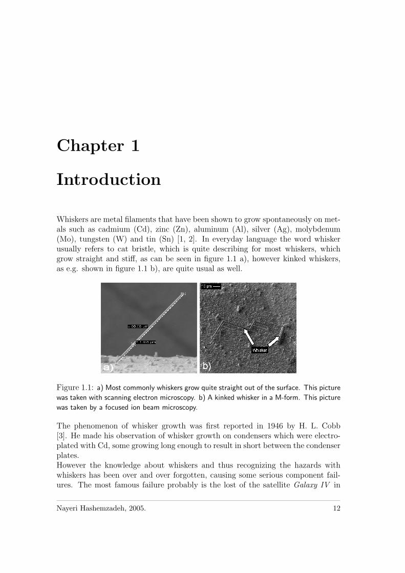
Whiskers are metal filaments that have been shown to grow spontaneously on met-als such as cadmium (Cd), zinc (Zn), aluminum (Al), silver (Ag), molybdenum(Mo), tungsten (W) and tin (Sn) [1, 2]. In everyday language the word whiskerusually refers to cat bristle, which is quite describing for most whiskers, whichgrow straight and stiff, as can be seen in figure 1.1 a), however kinked whiskers,as e.g. shown in figure 1.1 b), are quite usual as well.
Figure 1.1: a) Most commonly whiskers grow quite straight out of the surface. This picture
was taken with scanning electron microscopy. b) A kinked whisker in a M-form. This picture
was taken by a focused ion beam microscopy.
The phenomenon of whisker growth was first reported in 1946 by H. L. Cobb[3]. He made his observation of whisker growth on condensers which were electro-plated with Cd, some growing long enough to result in short between the condenserplates.However the knowledge about whiskers and thus recognizing the hazards withwhiskers has been over and over forgotten, causing some serious component fail-ures. The most famous failure probably is the lost of the satellite Galaxy IV in
Nayeri Hashemzadeh, 2005. 12

13
1998, the estimate worth of the satellite was 250 million dollar [4, 5]. There havebeen other serious failures reported due to whiskers in aircrafts, computer centersand medical devices [5].Most whiskers do not grow more than a few hundred micrometers, but whiskersof lengths up to 5 mm have been observed in this work.
Figure 1.2: Cross section overview of a molded semiconductor component.
The plague of whiskers could soon become even more evident if the right countermeasures are not taken. This is due to new regulations made by the EuropeanUnion as to restrict or ban lead (Pb) use in electronics depending on what theseapplications will be used for. This regulations are summarized under the name ofRestriction of Hazardous Substances Directives (RoHS) and are to be implementedacross the European Union from July the 1st 2006. The regulations applied forthe automotive industry go under the name of End of Life Vehicles and here thelegislation states that there should not be more than 60 g lead per vehicle regard-ing the soldered electronics, this excluding the battery of the vehicle. If this limitis exceeded, the manufacturer must supply cost free recycling of the parts thatcause the overstep.Until now most manufacturers have used a mixture of Sn-Pb alloys for solderingand coating their components. The Sn-Pb mixture makes the solder surface lessprone to whisker growth [1, 6, 7]. With the general demand to decrease Pb useand particularly due to RoHS manufacturers must find a replacement for Sn-Pbsolders.Pure Sn is the favored candidate for galvanic plating purposes. Both because ofthe low costs involved in making the switch from Sn-Pb plating to Sn plating andbecause of tin’s desirable properties regarding solder ability, ductility, conductivityand corrosion resistance. This has created a great need to try to prevent or dimin-ish Sn whisker growth. If manufacturers want to be able to do so, the propertiesof whiskers have to be better understood.

1.1. Purpose 14
1.1 Purpose
The purpose of this thesis was to better understand the root cause of Sn whiskergrowth and try to understand how to prevent or restrain Sn whisker growth. Thiswas set to be done by reviewing the theories that exist about this phenomenonas well as studying growth of whiskers on different sets of samples undergoingdifferent conditions.Another side to the thesis was to test and calculate on Sn whiskers electrical andmechanical properties. More specific, testing how much current Sn whiskers areable to sustain and how much vibration and how high mechanical shocks whiskerscan withstand.
1.2 Outline
The chapters are structured in the following manner:
• Chapter 2. In this chapter an overview of whisker properties, specially forSn whiskers is given. Properties of Sn and Cu that will be important for thiswork are also listed. A review of some of the theories that exist regardingwhisker growth is presented, with some calculations on these models. Inthe last section of the chapter some of the mitigation strategies that aresuggested against whisker growth are described.
• Chapter 3. In the first part of this chapter the devices that were commonlyused in different experiments are presented. The second part covers exper-iment specific devices, the samples as well as the methods that were usedduring the work.
• Chapter 4. In this chapter the results achieved are presented followed bysome discussions about the results. In the first section of this chapter resultsregarding the mechanical durability of Sn whiskers are presented. In thesecond section of the chapter test results of the current carrying ability of Snwhiskers are presented, and then some finite element method calculations arepresented. In the last section results from studying the growth of whiskerson different samples undergoing different test conditions are described.
• Chapter 5. In this chapter a more thorough discussion about the results ispresented. Connection is made with results achieved in other studies as wellas the theories that exist.

1.2. Outline 15
• Chapter 6. What will be the future of whisker growth research is discussedas well as the work that could follow the results of this master thesis.
Chapter 2
Theoretical Background
2.1 Fundamentals
To be able to understand why whiskers grow, it is important to understand theproperties of whiskers. Some models that have been proposed to explain the rootcause of why whiskers grow can be neglected because of their inability to explainthe properties that whiskers have shown. A review of some of the major theoriesregarding whisker growth will be given further on in this chapter. Some of thesetheories will seem to be less able to explain some of the results reported aroundwhiskers, given in the two following sections and in section 2.3, which covers someof the mitigation strategies suggested in literature against Sn whisker growth.For this work properties of Sn whiskers are mostly important. Properties of Cu isinteresting as well, both regarding the practical issues around this work as well asreviewing theories on Sn whisker growth.
2.1.1 General Properties of Whiskers
In 1952 Herring and Galt published a report showing the elastic and plastic prop-erties of Sn whiskers to be near what would be expected of perfect single crystals[8]. This has led to the conclusion that whiskers are nearby perfect crystals. Theythus also confirmed the theoretical calculations on the strength of perfect crystals[9]. Bulk materials show much less strength than perfect single crystals due tohigh numbers of dislocations and grains. Sheng et al. published 2002 Sn whiskersstudies done with Focused Ion Beam systems (FIB) showing that whiskers containmany defects, which they thought were mainly dislocations [10].Dunn published in 1986 results about the Young’s modulus of whiskers varyingdepending on which direction the whisker grow [11]. The values ranged between8 to 85 GPa. Dunn wrote about the difficulty of measuring the diameter andthe imperfection of assuming that the whiskers are cylindrical in the calculations.
Nayeri Hashemzadeh, 2005. 16
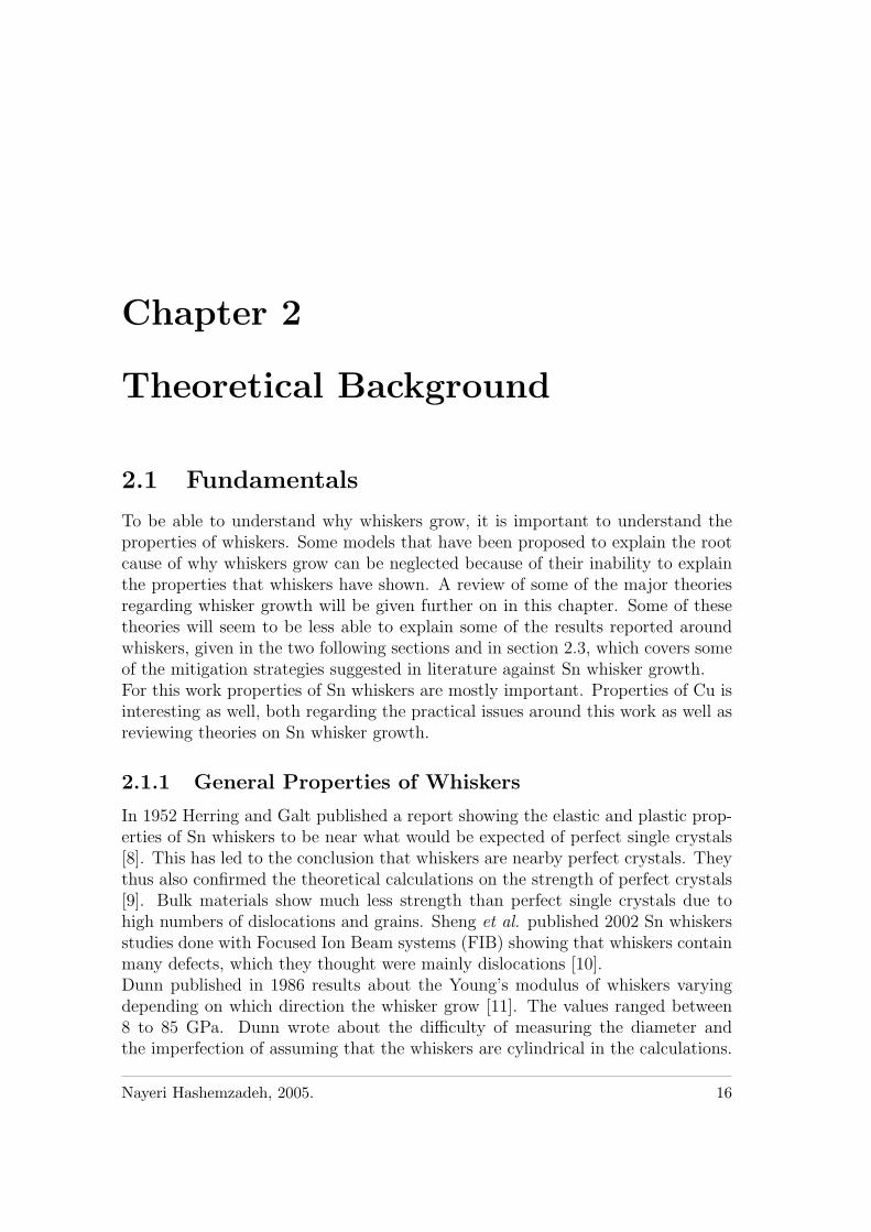
2.1. Fundamentals 17
Figure 2.1: The picture shows a whisker with an irregular cross section.
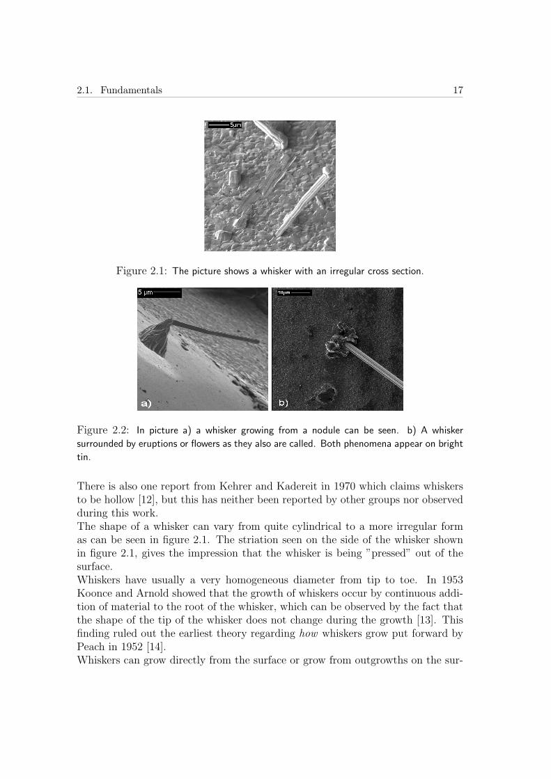
Figure 2.2: In picture a) a whisker growing from a nodule can be seen. b) A whisker
surrounded by eruptions or flowers as they also are called. Both phenomena appear on bright
tin.
There is also one report from Kehrer and Kadereit in 1970 which claims whiskersto be hollow [12], but this has neither been reported by other groups nor observedduring this work.The shape of a whisker can vary from quite cylindrical to a more irregular formas can be seen in figure 2.1. The striation seen on the side of the whisker shownin figure 2.1, gives the impression that the whisker is being ”pressed” out of thesurface.Whiskers have usually a very homogeneous diameter from tip to toe. In 1953Koonce and Arnold showed that the growth of whiskers occur by continuous addi-tion of material to the root of the whisker, which can be observed by the fact thatthe shape of the tip of the whisker does not change during the growth [13]. Thisfinding ruled out the earliest theory regarding how whiskers grow put forward byPeach in 1952 [14].Whiskers can grow directly from the surface or grow from outgrowths on the sur-

2.1. Fundamentals 18
face known as nodules which can be seen in figure 2.2 a). In figure 2.2 b) a whiskercan be seen surrounded by eruptions or flowers as they also are called. The lasttwo phenomena appear when Sn whiskers are growing on bright tin. Bright Sn isachieved by adding organic soluble to the galvanic bath. The grain structure inbright Sn is smaller than in dull Sn.It has been reported that the whiskers seem to have a period of a constant growthuntil the growth rate suddenly decreases greatly [15]. The growth rates that havebeen reported vary, but lie usually somewhere between 100 µm to 1 mm per year[15]. During this work whisker diameters between 1 µm to 6 µm have been ob-served and the longest whiskers observed were up to 5 mm, but for most whiskersthe length seem not to surpass more than a few 100 µm.
Figure 2.3: Phase diagram of the Cu-Sn systems. At room temperature the intermetallic
that forms is the η’-phase [18].

2.2. Tin Whisker Growth Models 19
2.1.2 Cu-Sn Properties
Tin has two allotropes at normal pressure, α-Sn and β-Sn [16]. Grey Sn as α-Snis usually referred to, is an intrinsic semiconductor and is stable at temperaturesbelow 13.2 oC. For this work only the metal form of Sn, that is β-Sn or white Sn,which is stable for temperatures above 13.2 oC, is interesting. White Sn has abody centered tetragonal crystal structure with the lattice constants of a = b =0.58318 nm and c = 0.31819 nm [17]. The molar weight of Sn is 118.71 g. Thedensity for β-Sn is 7310 kg/m3.Copper has a face centered cubic structure with lattice constants a = b = c =0.36149 nm and a molar weight of 63.546 g resulting in a density of 8920 kg/m3.The phase diagram for the intermetallic compound (IMC) that forms between Cuand Sn is shown in picture 2.3. For this work only phases which are stable attemperatures below the Sn melting point are interesting. At room temperatureCu6Sn5 (η’-phase) forms spontaneously and for temperatures above 100 oC therewill also be formation of Cu3Sn (ε-phase) at the expense of the η’-phase [19]. Theη’-phase has the density of 8270 kg/m3.In table 2.1 some of the electrical and mechanical properties of Sn and Cu, whichhave been used for the calculations of the durability of whiskers, can be found.
2.2 Tin Whisker Growth Models
As mentioned in chapter 1, the first reported observation of whiskers was on elec-troplated Cd in 1946 by Cobb [3], causing shorts on condensers. Eventually theseproblems lead Bell Telephone to change to pure tin electroplating in 1948, just tofind pretty soon that pure Sn showed the same type of problems. Consequentlythe first report on Sn whisker growth came from Bell Laboratories in 1951 [20].Since then most of the articles produced around the whisker growth phenom-
Tin CopperThermal conductivity at 300 K, (κ300K), [ W
m·K ] 65 400Specific heat capacity at constant pressure and 300 K, (Cp), [ J
kg·K ] 230 385Resistivity at 300 K, (ρ300K), [10−9 Ω ·m] 110 17Temperature coefficient, (α), [10−3 K−1] 4.63 4.33
Melting point at pressure 105 Pa, (Tm), [K] 505 1356Young’s modulus, (E), [109 Pa] 55 120
Shear modulus [109 Pa] 21 46Poisson ratio, (v) 0.36 0.34
Table 2.1: The properties of (bulk) Sn and Cu that are important for this work are puttogether [16, 17].
2.2. Tin Whisker Growth Models 20
enon have focused mostly on Sn whiskers. Some of the theories existing regardingwhisker growth are specifically made for Cu-Sn systems, e.g. the theory that willbe covered in section 2.2.3.
There are basically three different theories on why whiskers grow, i.e. what isthe driving force behind whisker growth. Within these theories there are differentsuggestions about how whiskers grow, i.e. what are the mechanisms of whiskergrowth. The driving forces for whisker growth can be classified into the followingclasses
1. Surface energy effects [21, 22]
2. Stored strain energy [23, 24, 25]
3. Internal mechanical stresses [10, 26, 27]
The three models above are listed in chronological order. First theory states thata local negative surface tension is the reason why whiskers grow. The stored strainenergy theory involves an abnormal recrystallization process. The third theoryabout internal mechanical stresses states that formation of intermetallic betweenthe base material and the tin layer causes stress in the tin.
2.2.1 Surface Energy Effects
Both J. D. Eshelby and F. C. Frank suggested independently in 1953 that a localnegative surface tension is the driving force for whisker growth [21, 22]. The energyrequired to form a fresh surface comes from the surface being attacked by theatmosphere resulting in a negative surface tension, γ. The simple thermodynamicequation for surfaces is given by
U = TS − pV + µN + γA, (2.1)
where U is the energy of the system, T is the temperature, S is the conventionalentropy, p is the pressure, V is the volume, µ is the chemical potential, N is thenumber of particles and A denotes the surface area [28].In most cases γ is positive which means in order to minimize the energy of thesystem, the surface has to be as small as possible. A local negative surface tensionhence provides the needed driving force for a whisker to grow.The authors suggested two different dislocation mechanisms to feed the whiskerwith the needed building material.Eshelby suggested that a Frank-Read source below a hump that is created by thenegative surface tension emits the dislocation loops that make the whisker grow[21]. The dislocation loop provided with the right amount of stress first expand to
2.2. Tin Whisker Growth Models 21
the radius of the whisker and then glide vertically, depositing one atomic layer atthe base of the hump, causing a whisker to grow.By making some assumptions, Eshelby reaches the following expression for thegrowth rate of the whisker:
∂h
∂t∼ κβnD(
b
l2)(
γb2
kBT), (2.2)
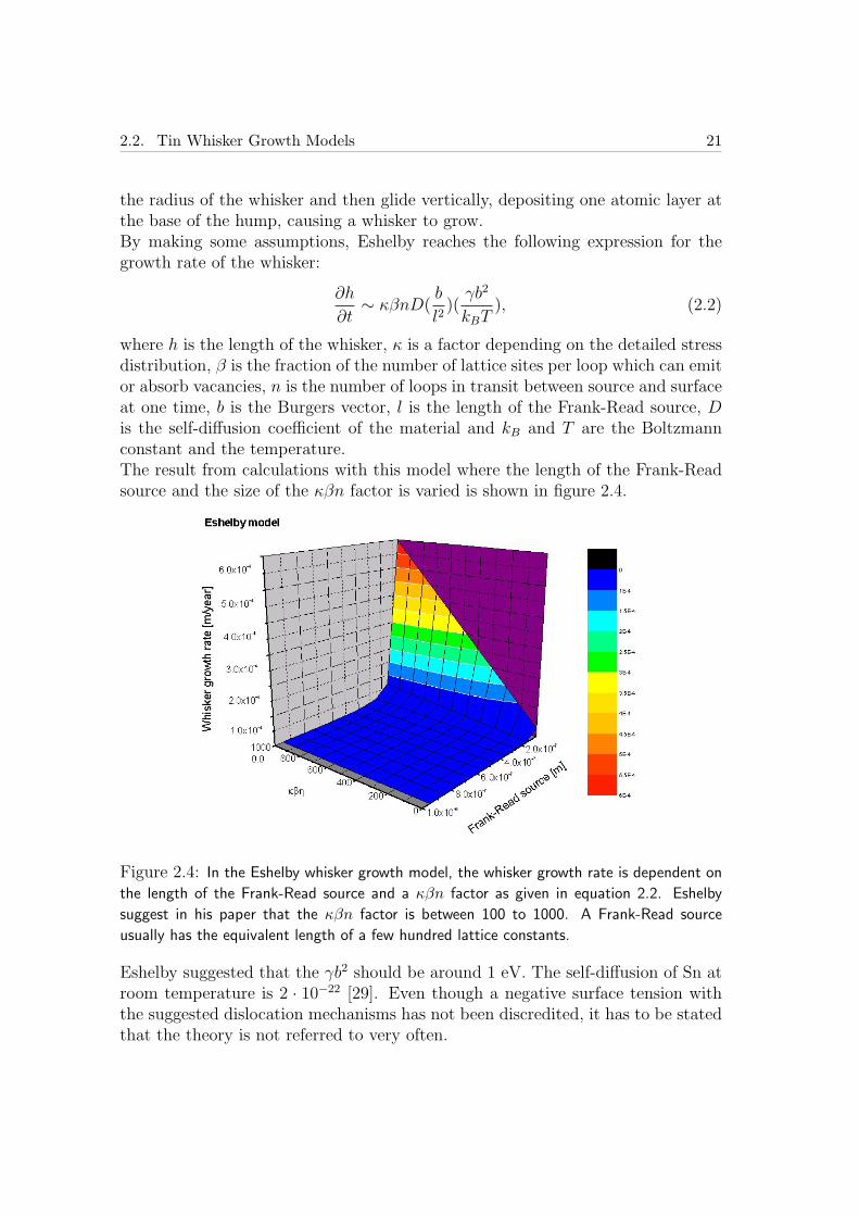
where h is the length of the whisker, κ is a factor depending on the detailed stressdistribution, β is the fraction of the number of lattice sites per loop which can emitor absorb vacancies, n is the number of loops in transit between source and surfaceat one time, b is the Burgers vector, l is the length of the Frank-Read source, Dis the self-diffusion coefficient of the material and kB and T are the Boltzmannconstant and the temperature.The result from calculations with this model where the length of the Frank-Readsource and the size of the κβn factor is varied is shown in figure 2.4.
Figure 2.4: In the Eshelby whisker growth model, the whisker growth rate is dependent on
the length of the Frank-Read source and a κβn factor as given in equation 2.2. Eshelby
suggest in his paper that the κβn factor is between 100 to 1000. A Frank-Read source
usually has the equivalent length of a few hundred lattice constants.
Eshelby suggested that the γb2 should be around 1 eV. The self-diffusion of Sn atroom temperature is 2 · 10−22 [29]. Even though a negative surface tension withthe suggested dislocation mechanisms has not been discredited, it has to be statedthat the theory is not referred to very often.

2.2. Tin Whisker Growth Models 22
2.2.2 Stored Strain Energy
Ellis et al. suggested in 1958 that an abnormal form of recrystallization processis the reason behind the whisker growth [23]. Recrystallization theory states thatlattice defects and grain boundaries rearrange in the bulk material at certain tem-peratures to minimize their energy. This is due to shear strain stored in the bulkmaterial resulting from plastic deformation in the material as it is formed [30].The recrystallization process is ordered in three principal stages:
• Recovery
• Recrystallization
• Grain growth
In the recovery stage, the dislocation density is diminished and energy is released.This process starts as soon as the Sn layer is plated. In the second stage, thatis recrystallization, new grains are formed. This stage can run parallel to the re-covery stage. Grain growth takes place in highly mismatched sites in relation tosurrounding material. In the last stage the grain boundaries are rearranged todecrease the grain boundary area. The number of grains decreases as well.It is suggested that this stage would be inhibited when whiskers grow. Grainboundaries lie usually perpendicular to the surface to decrease the curvature ofthe surface and hence are quite immobile. This effect is more apparent in thin-ner films where pinned grain boundaries at the surface can make all of the grainboundary area immobile. Therefore it is possible that at certain conditions growthof whiskers is more favorable to release the shear strain that is not released throughthe normal procedure of this last stage. Boguslavsky and Bush suggest that thereshould be preferred orientation of the grains that grow whiskers towards both thefree surface and neighboring grains [25].Another fact that makes recrystallization to an eligible candidate to promotewhisker growth is that recrystallization takes place for temperatures around 0.3-0.7 Tm, where Tm is the melting point of the metal. The metals that have shownwhisker growth at room temperature at normal conditions have the following melt-ing points [1, 16]
• Cd, Tm = 594K
• Sn, Tm = 505K
• Zn, Tm = 693K
The range of the recrystallization temperatures of these metals contains room tem-peratures.
2.2. Tin Whisker Growth Models 23
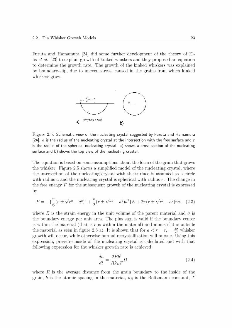
Furuta and Hamamura [24] did some further development of the theory of El-lis et al. [23] to explain growth of kinked whiskers and they proposed an equationto determine the growth rate. The growth of the kinked whiskers was explainedby boundary-slip, due to uneven stress, caused in the grains from which kinkedwhiskers grow.
Figure 2.5: Schematic view of the nucleating crystal suggested by Furuta and Hamamura
[24]. a is the radius of the nucleating crystal at the intersection with the free surface and r
is the radius of the spherical nucleating crystal. a) shows a cross section of the nucleating
surface and b) shows the top view of the nucleating crystal.
The equation is based on some assumptions about the form of the grain that growsthe whisker. Figure 2.5 shows a simplified model of the nucleating crystal, wherethe intersection of the nucleating crystal with the surface is assumed as a circlewith radius a and the nucleating crystal is spherical with radius r. The change inthe free energy F for the subsequent growth of the nucleating crystal is expressedby
F = −π
6(r ±
√r2 − a2)3 +
π
2(r ±
√r2 − a2)a2E + 2π(r ±
√r2 − a2)rσ, (2.3)
where E is the strain energy in the unit volume of the parent material and σ isthe boundary energy per unit area. The plus sign is valid if the boundary centeris within the material (that is r is within the material) and minus if it is outsidethe material as seen in figure 2.5 a). It is shown that for a < r = rc = 2σ
Ewhisker
growth will occur, while otherwise normal recrystallization will pursue. Using thisexpression, pressure inside of the nucleating crystal is calculated and with thatfollowing expression for the whisker growth rate is achieved:
dh
dt=
2Eb3
RkBTD, (2.4)
where R is the average distance from the grain boundary to the inside of thegrain, b is the atomic spacing in the material, kB is the Boltzmann constant, T
2.2. Tin Whisker Growth Models 24
is the temperature, and D is the self-diffusion coefficient of the material. Furutaand Hamamura used following number for their calculation of Sn whisker growth:E = 0.2J/cm3, D = 10−16 m2/s , T = 300K, R = 100 A and b3 = 30 A3 thegrowth rate is about 3 A/s or around 1 mm/year.
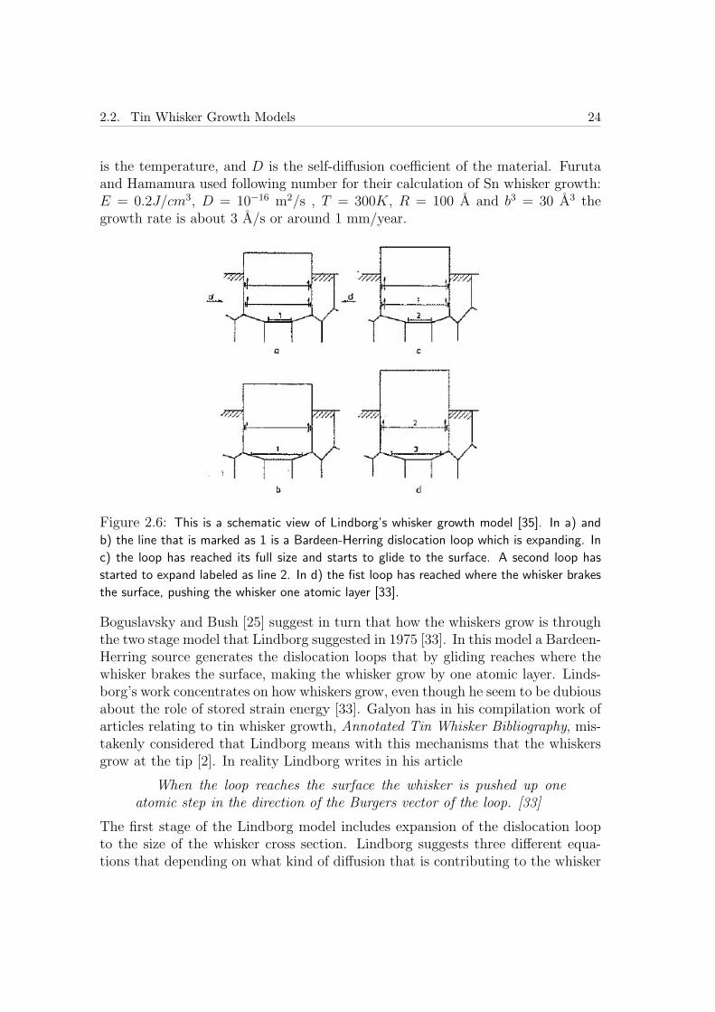
Figure 2.6: This is a schematic view of Lindborg’s whisker growth model [35]. In a) and
b) the line that is marked as 1 is a Bardeen-Herring dislocation loop which is expanding. In
c) the loop has reached its full size and starts to glide to the surface. A second loop has
started to expand labeled as line 2. In d) the fist loop has reached where the whisker brakes
the surface, pushing the whisker one atomic layer [33].
Boguslavsky and Bush [25] suggest in turn that how the whiskers grow is throughthe two stage model that Lindborg suggested in 1975 [33]. In this model a Bardeen-Herring source generates the dislocation loops that by gliding reaches where thewhisker brakes the surface, making the whisker grow by one atomic layer. Linds-borg’s work concentrates on how whiskers grow, even though he seem to be dubiousabout the role of stored strain energy [33]. Galyon has in his compilation work ofarticles relating to tin whisker growth, Annotated Tin Whisker Bibliography, mis-takenly considered that Lindborg means with this mechanisms that the whiskersgrow at the tip [2]. In reality Lindborg writes in his article
When the loop reaches the surface the whisker is pushed up oneatomic step in the direction of the Burgers vector of the loop. [33]
The first stage of the Lindborg model includes expansion of the dislocation loopto the size of the whisker cross section. Lindborg suggests three different equa-tions that depending on what kind of diffusion that is contributing to the whisker

2.2. Tin Whisker Growth Models 25
growth limit whisker growth rate. The three diffusion types are: lattice diffusion,grain boundary diffusion or diffusion through dislocation pipes. The slowest diffu-sion type is lattice diffusion and diffusion through dislocation pipes is the fastestone. Dislocation pipes are description of dislocations where the boundary of thedislocations is described as a ”pipe” with a certain radius [34]. Equation 2.5 is thegeneral form of the Lindsborg’s three whisker growth rate limiting equations:
dhx
dt= kx
σ
RwTDx, (2.5)
where kx depends on the diffusion source and different material properties, Rw isthe whisker radius, σ is the stress in the direction of the Burgers vector of theloop, T is the temperature and Dx denotes the type of diffusion that is in effect.The second stage is the gliding of the loop in direction of its Burgers vector, i.e.the direction of the growth of the whisker. The growth rate for the whisker isgiven by
dh2
dt= k2
(σ − k3
Lw
)n
, (2.6)
where k2 and n are both dependent on dislocation density and temperature but in-dependent of stress, k3 is dependent on the Burgers vector and the stress and Lw isthe space between dislocations. n varies between 10 to 20, making the equation 2.6highly stress dependent. This means that for high stress situation the first stage,that is generation of the dislocation loops would not keep up, and the whiskergrowth rate would then be governed by equation 2.5 where the stress dependenceis linear. It is also pointed out in Boguslavsky’s and Bush’s work [25] that dislo-cation distance, Lw, is larger in low angle grain boundaries giving a higher growthrate. At the same time they state that high angle grain boundaries, where thelattice mismatch is usually greater, provides for a faster grain boundary diffusion,which would make them more favorable to provide the Sn that is needed for thewhisker. They thus conclude that a balanced mix of low angle grain boundariesand high angle boundaries would provide the best settings for whisker growth.As it was pointed out earlier, Lindborg did not favor the stored strain energymodel, while he in a article that was published 1975 could not show that micros-train was an important factor for Zn whisker growth [35]. Rather he found thatinternal compressive macrostress was the driving force behind zinc whisker growth.Concluding that the stored strain energy is negligible.
2.2.3 Internal Mechanical Stresses
A theory about whisker growth in dependence on internal mechanical stresses wasput forward by K. N. Tu in 1994 [26]. In this paper Tu discussed whisker growth
2.2. Tin Whisker Growth Models 26
on Cu-Sn systems, which is the materials most important for this thesis. The basicidea is that whiskers grow because of stresses that are caused due to formation ofintermetallic compound (IMC) between copper and tin. It was shown by Tu in1973 that the reaction of Cu with Sn seems to have an effect on whisker growth[19]. It can be seen in the phase diagram for Cu-Sn system in figure 2.3 that theIMC that forms during room temperature is the η′-phase, Cu6Sn5. Tu suggestedthat an uneven IMC growth taking place at the η′-phase/Sn interface and mostlyin the grain boundaries of the Sn results in a compressive stress in the Sn filmwhich leads to whisker growth. He writes the following in his paper:
At room temperature we can assume that there is no diffusion of Sninto Cu since Sn diffuses substitutionally in Cu and the diffusivity isnegligible. [26]
This conclusion is based on the work of Butrymowicz et al. [36].Also in this model weak spots at the surface are assumed, where the tension thatotherwise is build up is released in form of whiskers. Tu suggested that these spotsare where the surface oxide is broken. As long as the stress is maintained in Snby the chemical reaction the whisker growth is sustained. For kinked whiskers Tusuggested that the surface oxide on one side of the whisker ”heals”, resulting inkinking the whisker until the oxide is cracked again.Tu calculated the rate of chemical reaction and the rate of the whisker growth.Gibbs free-energy change for the reaction is
dG = −SdT + V dp− Cdξ, (2.7)
where G is Gibbs free energy and ξ is a reaction variable for the extent of thereaction. C is the chemical affinity which is
C = µη′ − 6µCu − 5µSn, (2.8)
µ is here the chemical potential. From this a chemical driving force is calculatedand by making some assumptions and solving a differential equation Tu reachesthe following formula for the growth rate of the whisker
∆h
∆t=
2
ln(b/a)
σ0ΩsD
kBTa2, (2.9)
where 2b is the distance between two neighboring whiskers, a is the radius of thewhisker, σ0 is the stress at a distance of b from the whisker (this has been usedas boundary condition when solving the differential equation), Ω is the atomicvolume, s is the step height between the base atoms and D is the grain boundarydiffusivity of Sn at room temperature.

2.2. Tin Whisker Growth Models 27
Figure 2.7: This picture is taken from Tu’s paper in 1994. It is a sketch of the top view of
whiskers growing. In this model the whiskers would have a diameter of 2a and a spacing of
2b [26].
Figure 2.8 shows calculations made on this equation where parameter a which isthe radius of the whisker and b which is half of the distance to the nearest neighbor-ing whisker is varied. Otherwise same values that was used by Tu in his 1994 paperis used [26], σ0Ω = 0, 01eV , kBT = 0, 025eV at room temperature, s = 0, 3nmand the grain boundary diffusivity of Sn at room temperature, D = 10−12m2/s.As graph 2.8 shows the growth rate increases as the a and b come closer in value
Figure 2.8: This graph shows the whisker growth rate according to equation 2.9, based on
Tu’s model [26]. The whisker radius a and the spacing between each whisker 2b is varied.
to each other due to the ln(b/a) in the denominator.

2.2. Tin Whisker Growth Models 28
Volume Change
An important part of Tu’s suggested mechanism for whisker growth is the volumelost caused by the creation of Cu6Sn5. By using the density of the material orthe shape of the unit cell, the volume/atom for the Cu, Sn and Cu6Sn5 can becalculated.The density for Cu is 8920 kg/m3, the density for Sn is 7310 kg/m3 and thedensity for η′-pahse is 8280 kg/m3 [16, 37]. The atomic volume for Sn is around,VSn = 2.70 · 10−29 m3, for Cu it is VCu = 1.18 · 10−29 m3 and for the η′-phaseVη′ = 1.78 · 10−29 m3. This results in
11 ∗ Vη′
6 ∗ VCu + 5 ∗ VSn
≈ 95%.
Meaning a decrease in the total volume. However if it is considered that the growthof the η′-phase would almost only occur in the η′-phase/Sn interface and that thevolume change would only be on the cost of the Sn film the result is changed to
11 ∗ Vη′
5 ∗ VSn
≈ 145%.
This calculation shows that the growth of IMC in the Cu-Sn interface would causestress if the IMC boundary does not move deeper into the Cu substrate.Based on this calculation it is easy to calculate how much η′-phase is needed toprovide the material needed for a Sn whisker, assuming that all of the η′-phasegrowth would translate to Sn being pressed out as whiskers. An uneven growth ofIMC amounting to 0.1 µm η′-phase on an area of 100 µm times 100 µm wouldresult in an about 140 µm long whisker with a diameter of 2 µm. This simpleexample is only to visualize roughly how little IMC growth of η′-phase would beneeded to provide the Sn for the whisker.
Barsoum et al. published in 2004 an article where they proposed it is thereaction of oxygen with the metal that causes whiskers to grow [27]. In this modeldiffusion of oxygen into the metal and the following reaction with the metal givesa volume expansion that would cause stress, which would be relieved in the sameway as in Tu’s model [26].For Sn the possible reactions with O2 are
Sn +1
2O2 → SnO, (2.10)
Sn + O2 → SnO2. (2.11)
The density for SnO is 6450 kg/m3 and for SnO2 it is 6950 kg/m3 [17]. Theaverage atomic volume for SnO is VSnO = 1.73 · 10−29 m3 and for SnO2 it is

2.3. Mitigation Strategies 29
VSnO2 = 1.20 · 10−29 m3. The volume change is:
2 · VSnO
VSn
≈ 129%. (2.12)
3 · VSnO2
VSn
≈ 134%. (2.13)
It has to be pointed out that Barsoum et al. reached their conclusions after havingcoated some samples with polymer coating and keeping some samples in the freefor just three months. It has been reported that conformal coating as it is calledcould retards whisker growth but does not prevent it [38]. Also Guber has shown inhis master thesis in 2004 that there is no relation between thickness of the surfaceoxide and whisker growth [39].
2.3 Mitigation Strategies
Through the years different methods, besides mixing tin with lead, have beensuggested as mitigation strategies. Results concerning these strategies have beendifferent and some times even contradicting each other.The strategies most current for this work are:
1. Variation of the tin plating thickness. Already in 1963 it was shownthat by varying the Sn layer thickness whisker growth could be restrained[40]. Different intervals of Sn layer thickness have been suggested, withinwhich there will be whisker growth, while outside there is no whisker growth.Arnold suggested in 1966 such an interval to be for 0.5 µm > Sn layerthickness > 8 µm. [41].
2. Use of different base material. It has long been known that differentbase materials have shown different aptitude towards whisker growth [40].For instance there seems to be no growth of whiskers when tin is depositedon base material FeNi43 [42].
3. Use of an underlayer between the base material and the Sn layer.Use of an underlayer, also known as barrier layer, between the base materialand the tin layer is another way to try to control whisker growth. Nickel is theunderlayer most reported on as used between Sn and Cu, with some claimsof total prevention of whisker growth while others report only damping ofwhisker growth [5, 43, 44].
4. Reflowing the Sn surface. Reflowing the Sn surface, that is exceedingthe melting point of Sn, which is 232 oC, and thus melting the plated Sn hasalso been reported as a way to reduce whisker growth [43].

2.3. Mitigation Strategies 30
5. Annealing of the Sn layer after plating. Annealing, that is heatingunder the melting point of the Sn, is reported to drastically reduce whiskergrowth [45]. There are two theories on why this is achieved. One is thatannealing leads to a fast and even growth of IMC in Cu-Sn systems [26].The other explanation is that annealing releases the stored energy [25].
Chapter 3
Procedure
3.1 Instruments Used
In the first section of this chapter the instruments that were used in more thanone type of tests are presented. Following this section each type of tests and thecorresponding instruments and samples are presented.
3.1.1 Light Microscope
Two types of light microscopes were used during the work.
Model and Manufacturer MagnificationLight microscope 1: Ergolux from Leitz 50 – 500Light microscope 2: Axioskop 2 MAT from Zeiss 25 – 1000
The first light microscope (LM 1), was a simpler model which was not connectedto a computer with a camera.Light microscope 2 (LM 2), which was more frequently used, was connected to acamera of model Axiocam HRC with the computer software MaGraBo. This gavethe possibility to measure and take picture from the samples.
3.1.2 Scanning Electron Microscope
A scanning electron microscope (SEM) of model 1450 VP from LEO was used.Detailed information about how SEM functions can be found on internet or inliterature, e.g. Flewitt and Wild’s Physical Methods for Materials Characterisation[46].In this model a tungsten filament is used to generate the electrons that bombardthe surface. The secondary electrons with their low energy are detected, giving agood resolution of the surface. There is also the possibility to use a filter to detect
Nayeri Hashemzadeh, 2005. 31
3.1. Instruments Used 32
the backscattered electrons that have a higher energy, to get a better contrastbetween the different materials on the surface.The electrons can be accelerated to an energy of 50 keV . The apparatus is saidto be able to theoretically to give 800 000 times magnification, but in reality thequality of the pictures limits the magnification to 10 000 times. The resolution is20 nm.
Energy Dispersive X-ray spectroscope
The 1450 VP is equipped with an Energy Dispersive X-ray spectroscope (EDX).Information about how EDX functions can be found on internet or in literature,e.g. Flewitt and Wild’s Physical Methods for Materials Characterization [46].With this EDX, one could detect elements as light as Boron.
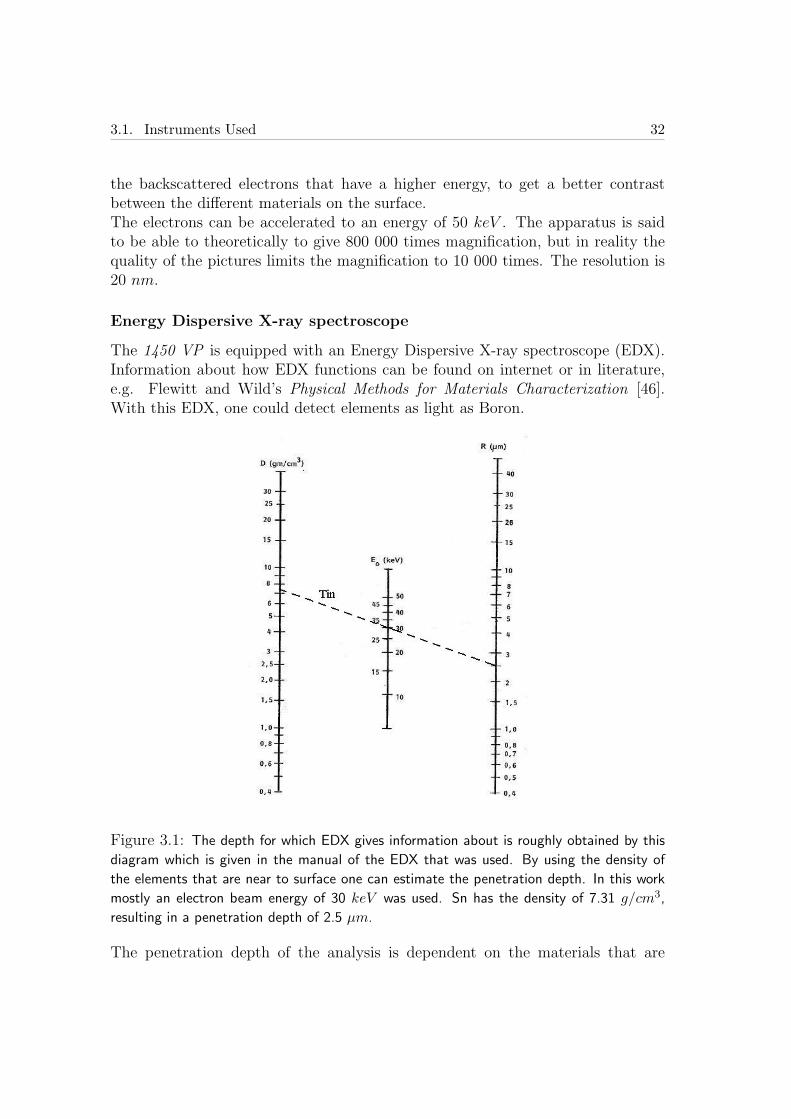
Figure 3.1: The depth for which EDX gives information about is roughly obtained by this
diagram which is given in the manual of the EDX that was used. By using the density of
the elements that are near to surface one can estimate the penetration depth. In this work
mostly an electron beam energy of 30 keV was used. Sn has the density of 7.31 g/cm3,
resulting in a penetration depth of 2.5 µm.
The penetration depth of the analysis is dependent on the materials that are
3.2. Measuring Mechanical Durability 33
investigated and the kinetic energy of the electrons in the beam. Figure 3.1 showshow this information can be obtained. Roughly one can say that elements thatmake up less then 1% of the weight of the composition will not be noticed in theEDX diagram.
3.2 Measuring Mechanical Durability
3.2.1 Stereo Microscope
Stereo Microscope of Wild Peerbrugg was used with the camera Axiocam MRC5,together with the computer software MaGarBo.Stereo microscope was used for looking at samples that were hard to look at withordinary light microscope due to their dimensions. Here the highest resolutionthat can be achieved is 50 times. It is however not possible to measure lengthswith this microscope.
3.2.2 Vibration and Shock Table
To test the vibration endurance of the whiskers two vibration tables were used.
Vibration table 1: RMS, SW1507Accelerometer: Enevco SN 40021, Sensitiveness: 1.041 [mV/(m/s2]
Vibration table 2: RMS, SW8130Accelerometer: Enevco SN 40021, Sensitiveness: 1.041 [mV/(m/s2]
The two tables have different weights, table 2 being the heavier one. This doesnot influence the result of the vibration tests. The vibrations are produced fora combination of all directions and they reach up to 4500 Hz, depending on howhigh is the power spectral density (PSD [(m/s2)2/Hz)]). The PSD describes therelation between the acceleration and the frequency produced. This is measuredby the accelerometer and registered in a computer.For the mechanical shock resilience test table 2 was used because it can producehigher shocks.
3.2.3 Vibration and Shock Tests
Experiments were carried out to test the resilience of whiskers against vibrationsand shocks. Two different types of samples were used in these tests.Sample 1, shown in figure 3.2, showed growth of two large whiskers which werestudied by the stereo microscope. One whisker had grown a distance of 800 µm,from one pin to the other creating a short and the other whisker was about 350 µm

3.2. Measuring Mechanical Durability 34
Figure 3.2: This sample, noted as sample 1, was used as to test whiskers endurance against
vibrations and shocks. The sample is a sensor with pins that are coated with bright Sn.
It can more clearly be seen in b) that a long whisker has grown from one pin to another,
causing a short.
long.
Figure 3.3: This sample, noted as sample 2, was used to test whisker endurance against
vibrations. On this sample growth of many whiskers was observed. The whiskers growing
out from the edge of the sample were counted and measured for each pin to see if vibration
would make the amount of whiskers less.
Sample 2, shown in figure 3.3, had many whiskers on it. The whiskers on theedges of each pin which were longer than 30 µm were counted and measured withlight microscope 2 (see section 3.1.1). All together about 1000 whiskers were notedon the edges of the sample.First vibration tests were done with duration of 5 minutes on vibration table 1(see section 3.2.2, page 33). The vibration generated were random and as follows:
• 0.1 (m/s2)2/Hz, 0.2 (m/s2)2/Hz and 0.3 (m/s2)2/Hz, frequencies: 10-4500Hz
• 0.4 (m/s2)2/Hz, frequencies: 10-3970 Hz (limit of vibration table)
3.3. Measuring Electrical Durability 35
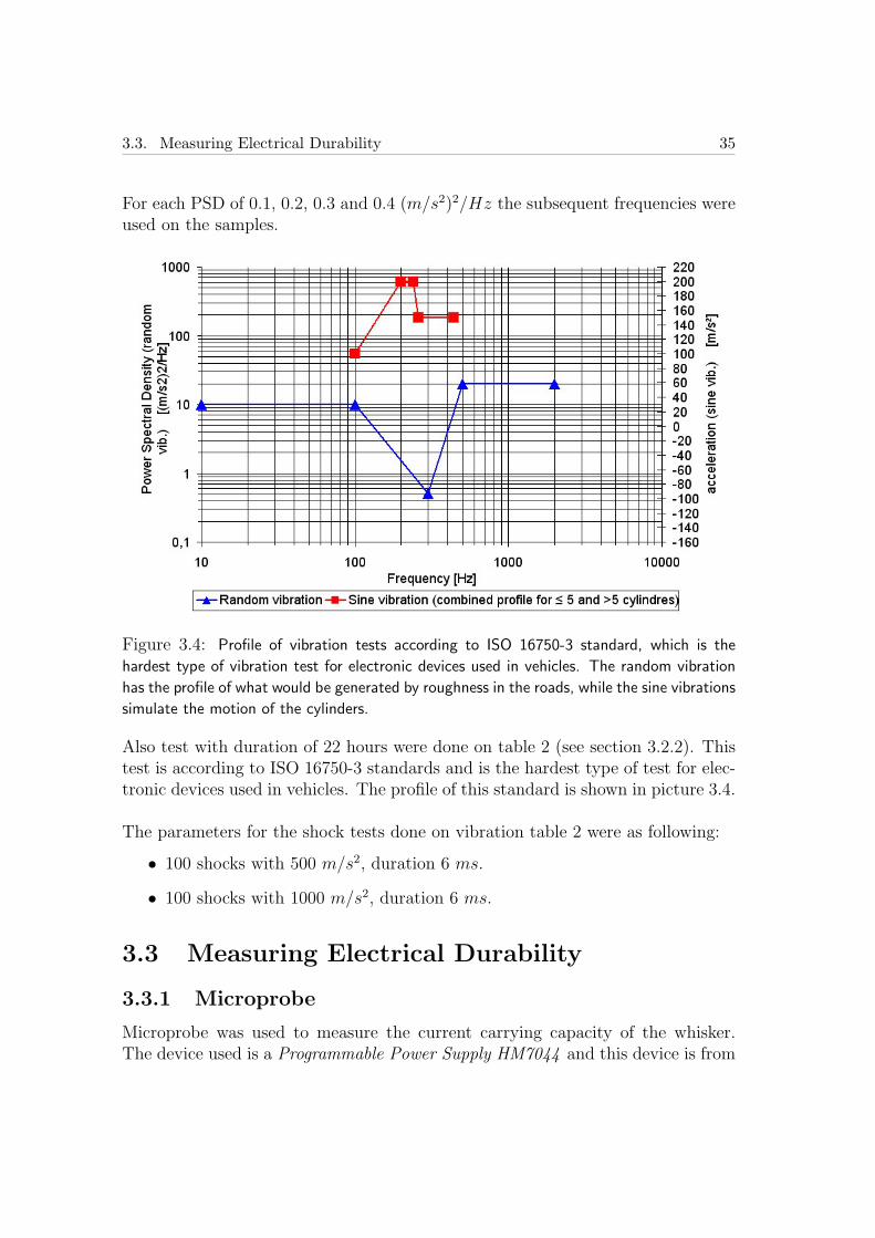
For each PSD of 0.1, 0.2, 0.3 and 0.4 (m/s2)2/Hz the subsequent frequencies wereused on the samples.
Figure 3.4: Profile of vibration tests according to ISO 16750-3 standard, which is the
hardest type of vibration test for electronic devices used in vehicles. The random vibration
has the profile of what would be generated by roughness in the roads, while the sine vibrations
simulate the motion of the cylinders.
Also test with duration of 22 hours were done on table 2 (see section 3.2.2). Thistest is according to ISO 16750-3 standards and is the hardest type of test for elec-tronic devices used in vehicles. The profile of this standard is shown in picture 3.4.
The parameters for the shock tests done on vibration table 2 were as following:
• 100 shocks with 500 m/s2, duration 6 ms.
• 100 shocks with 1000 m/s2, duration 6 ms.
3.3 Measuring Electrical Durability
3.3.1 Microprobe
Microprobe was used to measure the current carrying capacity of the whisker.The device used is a Programmable Power Supply HM7044 and this device is from
3.3. Measuring Electrical Durability 36
HAMEG Instruments. A voltage was applied in the tests and the current wasmeasured and plotted with a PC. It is possible to set a compliance current that isthe limit to how high the generated current can be. The highest allowed currentfor the device was 0.1 A. The Microprobe is equipped with a microscope that givesmagnification of up to 500 times.
3.3.2 Electrical Conductivity Tests
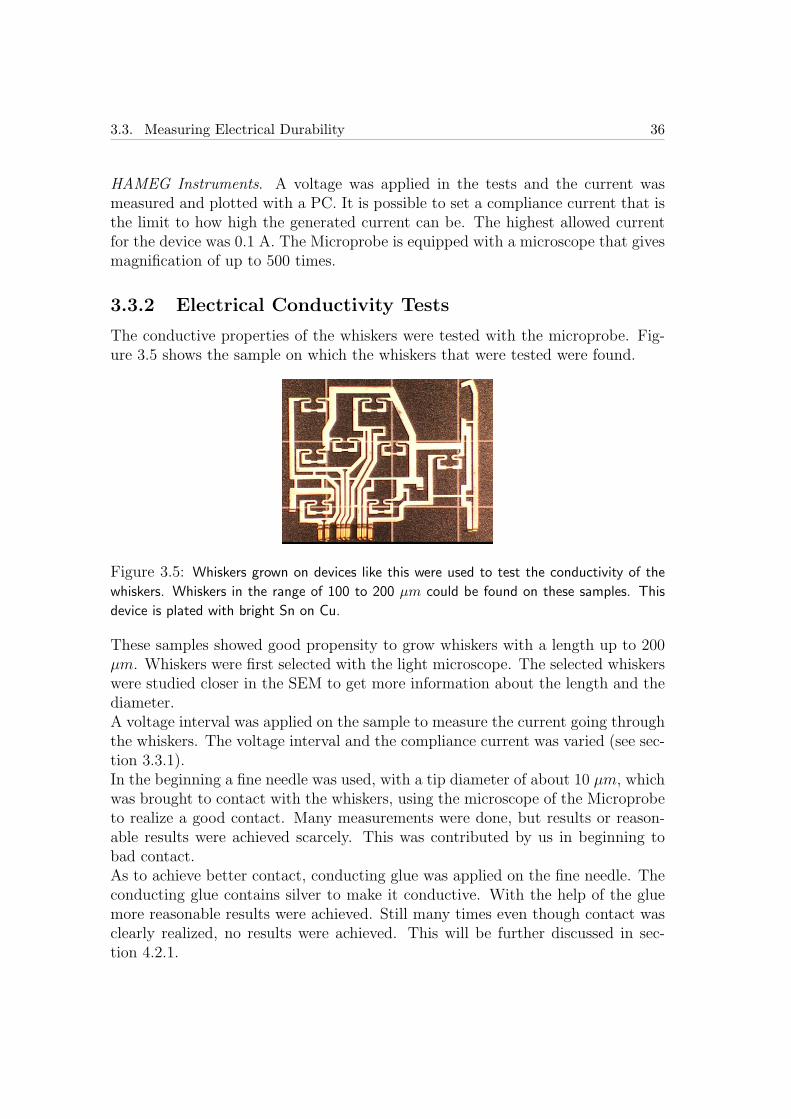
The conductive properties of the whiskers were tested with the microprobe. Fig-ure 3.5 shows the sample on which the whiskers that were tested were found.
Figure 3.5: Whiskers grown on devices like this were used to test the conductivity of the
whiskers. Whiskers in the range of 100 to 200 µm could be found on these samples. This
device is plated with bright Sn on Cu.
These samples showed good propensity to grow whiskers with a length up to 200µm. Whiskers were first selected with the light microscope. The selected whiskerswere studied closer in the SEM to get more information about the length and thediameter.A voltage interval was applied on the sample to measure the current going throughthe whiskers. The voltage interval and the compliance current was varied (see sec-tion 3.3.1).In the beginning a fine needle was used, with a tip diameter of about 10 µm, whichwas brought to contact with the whiskers, using the microscope of the Microprobeto realize a good contact. Many measurements were done, but results or reason-able results were achieved scarcely. This was contributed by us in beginning tobad contact.As to achieve better contact, conducting glue was applied on the fine needle. Theconducting glue contains silver to make it conductive. With the help of the gluemore reasonable results were achieved. Still many times even though contact wasclearly realized, no results were achieved. This will be further discussed in sec-tion 4.2.1.
3.3. Measuring Electrical Durability 37
Test have also been carried out by using a Cu pin coated with Sn, instead of aneedle. No contact glue was used in these tests.
3.3.3 Finite Element Method
Finite Element Method (FEM) was used to simulate the critical current, Icrit, atwhich whiskers are fused. The program Ansys was used to make the simulations.FEM is used for solving complicated physical problems by dividing the physicalmodel into simpler elements with homogeneous boundary conditions. The pro-gram solves the partial differential equation for each element and puts the resultstogether to determine the reaction of the whole geometry.The simulation was done for a cylindrical whisker in contact with two pins of Cu,perpendicular to the surface of both of the pins. The environment was taken tobe vacuum for simplification.The whisker was divided in 200 elements and the pins were divided in 300 elementseach making the total amount of elements in the model to be 800. Simulationswere done with more elements, showing that adding more elements to the modeldid not change the result considerably, but made the simulations slower.Besides the thermodynamic heat transfer equations used in the program someother relations were specified. This was the temperature dependence of electri-cal resistivity ρ(T ) which gives also the temperature dependence of the thermalconductivity through the Widemann-Franz law [16]:
ρ(T ) = ρ300K ∗ (1 + α(T − 300)). (3.1)
where ρ300K is the electrical resistivity at 300 K, T is temperature and α is thetemperature coefficient. Values of ρ300K and α can be found in table 2.1, page 19.The Widemann-Franz law for metals is:
K(T ) =LT
ρ(T ), (3.2)
where L = 2, 44 ∗ 10−8 [V 2/K2] is the Lorenz number and K(T ) is the thermalconductivity.Results from experiments were used to make a fit between Icrit measured for dif-ferent diameters and lengths of whiskers and the highest temperature achieved inthe simulated whisker. In this way a fusing temperature for the simulations wasdefined which differs from the melting temperature given in literature for Sn.

3.4. Studying Whisker Growth 38
3.4 Studying Whisker Growth
3.4.1 Focused Ion Beam
The Focused Ion Beam (FIB) system used was from Fei, model FIB 200. Detailedinformation about how FIB systems function can be found on internet or in lit-erature, e.g. Flewitt and Wild’s Physical Methods for Materials Characterisation[46].This FIB uses Ga+ ions to bombard the samples. The secondary electrons aredetected to get a picture. The ions are accelerated by 30 kV and the current usedto get a picture of the sample lies between 4 pA to 70 pA. Magnification of about100 000 times can be achieved. For this work the magnifications of up to 50 000times have been used. The pictures taken have been taken from an angle of π/4radians to the surface of the sample. This means that in the vertical direction theshapes of the sample appear 1/
√2 shorter than they are.
One can also make cuts on the sample by using higher ion currents. The currentsused to make a cut on the sample, that is to gradually etch away the surface ma-terials are between 6300 pA to 11 500 pA. Cuts on dimensions as little as 0.5 µmcan be made. Before making a cut a layer of platinum (Pt) was deposited in FIB,as to protect the surface. This is made by releasing a gas containing Pt atoms overthe surface of the sample. By shooting a current of 350 pA to 1000 pA the bondsbetween the Pt atoms are broken and the Pt is precisely deposited.
Figure 3.6: Schematic of the cross section of the samples studied.
Base Material Underlayer Sn Layer Heat TreatmentCuSn0.15 - Dull Sn 3-5 µm -CuSn6 Ni = 0.15 µm Dull Sn 10-12 µm 180 oC, 5 minE-Cu58 Ni = 2 µm Bright Sn 3-5 µm
Ag = 0.15 µm Bright Sn 10-12 µm
Ag = 2 µm
Table 3.1: The parameters that were combined for the 48 different types of samples.

3.4. Studying Whisker Growth 39
3.4.2 Sample Specifics
576 samples were prepared in the end of June 2004 to investigate whisker growth.The 576 samples were of 48 different types, i.e. they were arranged in 12 differentgroups undergoing different test conditions. The 48 different types of samples haddifferent nominal layer systems and post plating treatments. A schematic of thecross section of the samples showing the layer systems can be seen in figure 3.6.The list of the 48 types of samples that were ordered can be found in the appendix,table A.3, in page 68. Table 3.1 shows an overview of the parameters that werechanged for the different samples.More information about the plating process can be found in the appendix, ta-ble A.4, page 69. The 12 different groups have been undergoing different com-binations of conditions as can be seen in the appendix, table A.1, page 67. Theconditions are the following:
• Soldering simulation: Reflowing the Sn plated surface, i.e. heating up thesurface to 260 oC, which is above the Sn melting point
• Temperature Cycling: 500 cycles between -60 oC to 60 oC
• High Temperature Storage: 50 oC
• Room Temperature Storage: 22 oC
• Humidity: 1000 h storage under humid conditions, 85 % relative humidityand at 50 oC
Figure 3.7 shows a schematic overview of how the samples were delivered to us,where the dashed lines present how we divided each delivered part into threesamples.
Figure 3.7: A schematic of the coated parts the way they were delivered. The dimension of
the part is 3×1 cm. The dashed line presents how each part was divided into three samples.
The hole on the upper part is made for the bath process to dip it into the galvanic bath.

3.4. Studying Whisker Growth 40
3.4.3 Sample Study
After a storage of about six months the samples were thoroughly examined, mainlywith the help of LM 2 ( see section 3.1.1), to detect whisker growth. A gradingsystem was made to judge the level of whisker growth, as can be seen in table 3.2.
1 No whiskers could be observed2 Hillocks or very small whiskers observed3 Whiskers were observed, few and short4 Whiskers were observed to grow with high density or being very long5 Many long whiskers were observed
Table 3.2: The grading system that was used to judge whisker growth on the samples.
The whiskers found were measured and the longest whisker was noted in a tablethat will be discussed further more in the results section. It has to be noted thatthe measured length of the whiskers is only the length of the projection of thewhisker in the horizontal plane and therefore depends highly on how the whiskergrows out of the surface.It was discovered that whisker growth on the samples was rather inhomogeneous.Therefore grades with mixed number were also used to mark that fact.After optical investigation of all of the samples, some samples were chosen for acloser study with FIB system. One or two FIB cuts were made on the samples tostudy the whisker- and layer cross sections. First a layer of Pt was deposited with acurrent of 350 pA in the FIB system. The dimensions of the layer varied regardinghow deep the cut was meant to be, but usually it was around 30µm× 7µm with athickness of about 1 µm. The depth of the cuts were usually around 15 µm. Thecuts were done in a first step by a current of 11 500 pA, which gives a faster cutbut a more rough one. To make the cross section finer, a current of 6 500 pA wasused. Pictures were taken by a current of 4 pA or 11 pA in.To measure the average IMC and Sn thickness from the pictures taken with theFIB, the thickness of each layer was measured on 20 places, equidistant from eachother. As explained before, the pictures taken by FIB were taken under an angleof π/4 rad from the surface, so the measured thickness were multiplied with
√2.
These samples were further studied by help of the SEM and EDX. This as to getinformation on the density of whisker growth in the surroundings of the FIB cut,as well as the material composition of the surface around the FIB cut.Measurement of whisker density was done in SEM on some of the samples thatwere studied in FIB as to see how much whisker growth there was in the nearvicinity of the cut. This was done was by centering the SEM picture on the FIBcut with a magnification of 150 times, resulting in an area of about 760 µm times

3.4. Studying Whisker Growth 41
420 µm visible in the monitor. The whiskers that were seen in this area weremeasured. Out of this a whisker volume per area could be calculated.EDX analysis was done in the same way, with a magnification of 500 times and workdistance of roughly 20 mm with a fairly sharp contrast to get a measurement of thecomposition of the surface material. The information depth of these measurementsare roughly 2 µm.
Chapter 4
Results
4.1 Mechanical Durability
Whiskers can cause shorts in electronics. This can happen principally in threeways:
• a whisker can grow from one electrical contact to another
• two whiskers can grow on two different electrical contacts, and come in con-tact with each other
• a whisker could break and fall off, making a short somewhere else on thecircuit board.
Vibrations with frequencies around the natural frequency of the whisker may causea whisker to break. Calculations on the natural frequency of whiskers and testson whiskers resilience against vibrations and shocks will be presented.
4.1.1 Natural Frequency of Whiskers
The natural frequencies of whiskers can be calculated with the Euler-BernoulliBeam theory. These calculations can be found in Appendix B, page 70.For a cylindrical whisker that grows perpendicular to the surface with one end freethe natural frequency equation is
f =1.882
8π√
ρ
√Ed
L2. (4.1)
Here f is the natural frequency , d the diameter , L the length, E the Young’smodulus of the whisker and ρ is the density of the whisker. Figure 4.1 showscalculations that were made on this model with help of Matlab, and plotted by
Nayeri Hashemzadeh, 2005. 42
4.1. Mechanical Durability 43
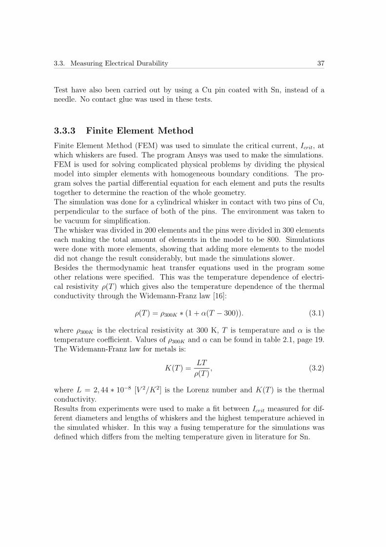
using the program Origin. A more precise table can be found in the appendix,table B.1, page 74.
Figure 4.1: Calculations made on the natural frequency of a cylindrical whisker. The length
and the elasticity modulus are varied, while the diameter is set to, d = 2 µm. The frequency
f ∝ d.
Whisker Length Natural Freqeuncy Natural Frequency[µm] free at one end [Hz] connected at both ends [Hz]
800 (Sample 1) 460-1490 3250-10600350 (Sample 1) 2390-7790 -
30-200 (Sample 2) 7320-≈ 5 ∗ 105 -
Table 4.1: Natural frequency range for the group of the whiskers that were tested with anestimated diameter of 2 µm. Only the whisker of size 800 µm is connected at both ends.
If the whisker has grown to connect perpendicular to another electrical contactand both ends are set to be equal, the natural frequency is then 6.36 times biggerthan the frequency resulting from equation 4.1. These calculations can also befound in the appendix B.1.1.
4.1.2 Results from Vibration Tests
Tests were carried out as described in section 3.2. As can be seen in figure 3.2the whisker of a length of 800 µm found on sample 1 is in contact with the other
4.1. Mechanical Durability 44
pin, thus the natural frequency would change as discussed previously. Table 4.1shows the range the natural frequency of these whiskers should lie according tothe calculations made.As described in section 3.2 in the first set of tests that had duration of 5 minutes,the samples were tested for frequencies up to 4500 Hz. As can be seen in table 4.1frequencies as high as 4500 Hz could contain the natural frequency of the whiskersof the sample 1, i.e. if the Young’s modulus of the two whisker would be smallenough. Nevertheless none of the two whiskers on the first sample broke off afterthe first set of tests. Neither did the number of whiskers on sample 2 decreaseafter these tests, which is consistent with the fact that the natural frequency ofthe whiskers on sample 2 were not reached.The second test with a duration of 22 hours and conditions according to the hardeststandard vibration test done for electronics used in automotive industry with thehighest frequency of 2000 Hz was done on sample 1. None of the two whiskersbroke off after this test either, ruling out the necessity of doing this test for thesecond sample.
4.1.3 Results from Shock Tests
Shock tests were performed on sample 1 with 100 shocks, each with a duration of6 ms and accelerations of 500 and 1000 m/s2. None of the whiskers broke. This isin good accordance with tests performed by Dunn in 1988 [11]. He reported thatwhiskers with lengths up to 1 mm withstood shock loads up to 2000 g, g being thegravitation constant of the earth.
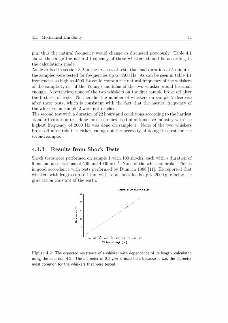
Figure 4.2: The expected resistance of a whisker with dependence of its length, calculated
using the equation 4.2. The diameter of 2.5 µm is used here because it was the diameter
most common for the whiskers that were tested.

4.2. Electrical Durability 45
4.2 Electrical Durability
Tests were performed to investigate how much electrical current whiskers can carry.Based on the results achieved FEM was used in Ansys program to simulate thecritical current at which whiskers fuse.
4.2.1 Electrical Conductivity of Whiskers
As described in section 3.3 it was difficult to achieve results measuring the electricalconductivity of the whiskers. This difficulties are presumably caused by a nonconductive surface oxide. The variation of the resistance in different measurementsfor the same whisker is also contributed to the surface oxide.The resistance of the test setup was measured by bringing the needle or the pindirectly in contact with the surface of the sample. This measured resistance is inseries with the resistance of the whisker. The lowest achieved resistance of the testsetup was 0.1 Ω which is subtracted from the results.The expected resistance of the whiskers can be calculated using the resistivity ofSn, (ρ = 110 · 10−9Ωm [16]).
R = ρL
A(4.2)
Here L is the length of the whisker, and A is the cross section area. In figure 4.2the expected resistance for a whisker with a diameter of 2.5 µm in dependence onits length is shown.
Length [µm] 60 115 240 115 70 170 105 80 140 55 200Diamter [µm] 2.5 2.5 2.5 2.5 2.8 2.5 1.6 1.9 5.5 1.6 3.3Resistance [Ω] 0.4 0.7 6.7 6 3 14 23 14 34 30 30
Resistivity [10−9Ωm] 17 30 140 260 260 400 440 480 580 1100 1200
Table 4.2: In this table the lowest measured resistance for different whiskers are presented.
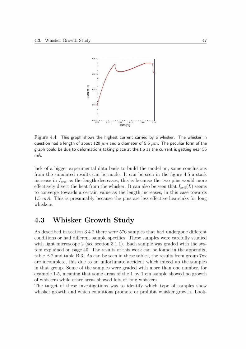
Table 4.2 shows the results of the resistivity and resistance of some of the whiskerstested. In most cases the measured resistivity was higher than ρ = 110 · 10−9Ωm,but there is also cases where the resistivity is lower than expected for Sn. Due todifficulties mentioned not many graph where one actually can see at which currentthe whiskers get fused were achieved, figure 4.3 shows such a graph. Table 4.3shows the fusing currents for investigated whiskers.The highest current carried by a whisker was 55 mA as seen in figure 4.4. Thiswhisker had a diameter of about 5.5 µm and a length of about 120 µm. Try todo tests with higher compliance currents than 55 mA eventually rendered in thefusing of the whisker. The values in table 4.3 shows the fusing currents achievedin the tests.
4.2. Electrical Durability 46
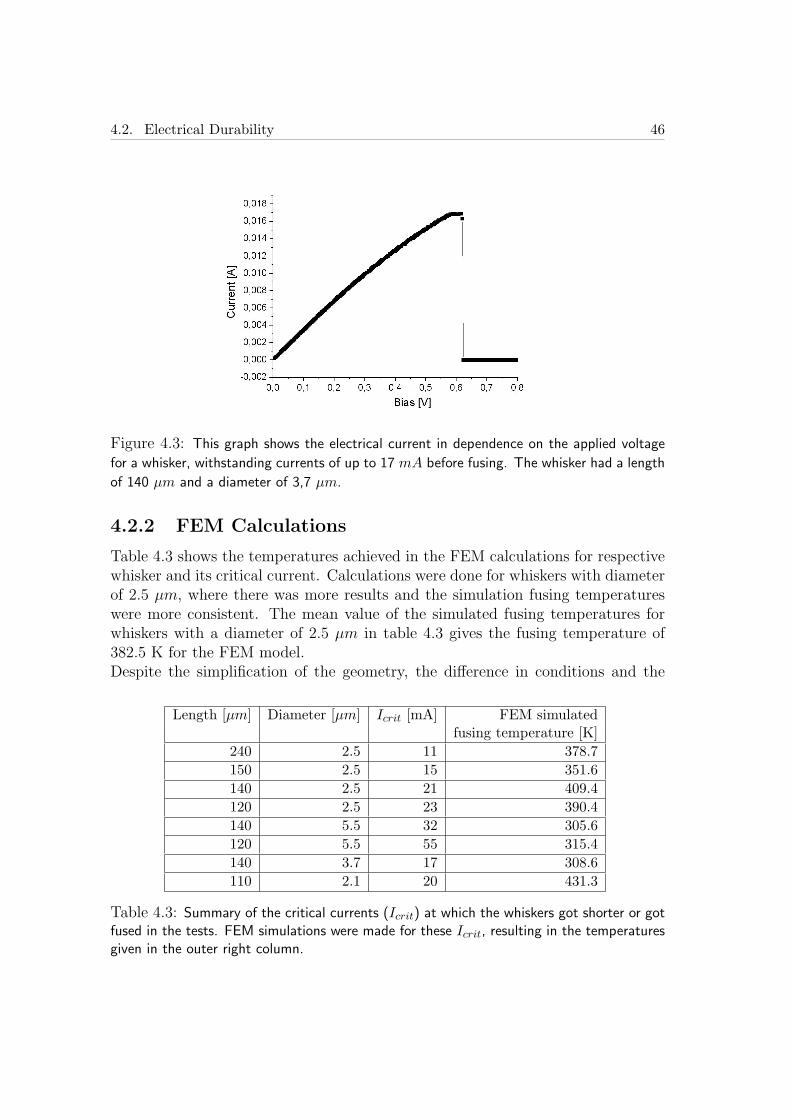
Figure 4.3: This graph shows the electrical current in dependence on the applied voltage
for a whisker, withstanding currents of up to 17 mA before fusing. The whisker had a length
of 140 µm and a diameter of 3,7 µm.
4.2.2 FEM Calculations
Table 4.3 shows the temperatures achieved in the FEM calculations for respectivewhisker and its critical current. Calculations were done for whiskers with diameterof 2.5 µm, where there was more results and the simulation fusing temperatureswere more consistent. The mean value of the simulated fusing temperatures forwhiskers with a diameter of 2.5 µm in table 4.3 gives the fusing temperature of382.5 K for the FEM model.Despite the simplification of the geometry, the difference in conditions and the
Length [µm] Diameter [µm] Icrit [mA] FEM simulatedfusing temperature [K]
240 2.5 11 378.7150 2.5 15 351.6140 2.5 21 409.4120 2.5 23 390.4140 5.5 32 305.6120 5.5 55 315.4140 3.7 17 308.6110 2.1 20 431.3
Table 4.3: Summary of the critical currents (Icrit) at which the whiskers got shorter or gotfused in the tests. FEM simulations were made for these Icrit, resulting in the temperaturesgiven in the outer right column.
4.3. Whisker Growth Study 47
Figure 4.4: This graph shows the highest current carried by a whisker. The whisker in
question had a length of about 120 µm and a diameter of 5.5 µm. The peculiar form of the
graph could be due to deformations taking place at the tip as the current is getting near 55
mA.
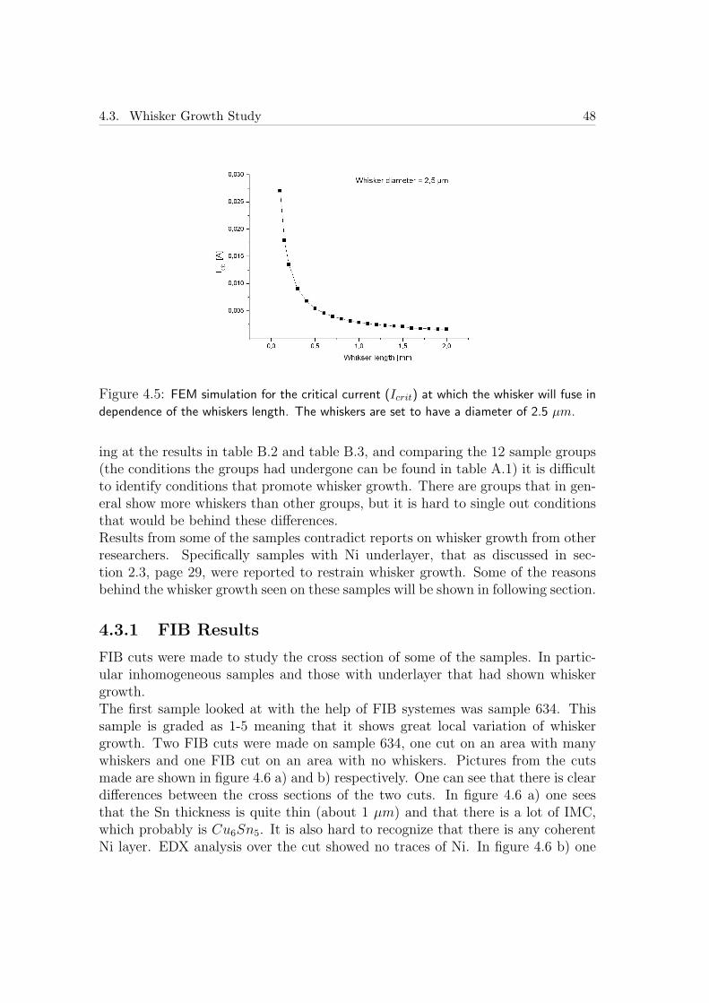
lack of a bigger experimental data basis to build the model on, some conclusionsfrom the simulated results can be made. It can be seen in the figure 4.5 a starkincrease in Icrit as the length decreases, this is because the two pins would moreeffectively divert the heat from the whisker. It can also be seen that Icrit(L) seemsto converge towards a certain value as the length increases, in this case towards1.5 mA. This is presumably because the pins are less effective heatsinks for longwhiskers.
4.3 Whisker Growth Study
As described in section 3.4.2 there were 576 samples that had undergone differentconditions or had different sample specifics. These samples were carefully studiedwith light microscope 2 (see section 3.1.1). Each sample was graded with the sys-tem explained on page 40. The results of this work can be found in the appendix,table B.2 and table B.3. As can be seen in these tables, the results from group 7xxare incomplete, this due to an unfortunate accident which mixed up the samplesin that group. Some of the samples were graded with more than one number, forexample 1-5, meaning that some areas of the 1 by 1 cm sample showed no growthof whiskers while other areas showed lots of long whiskers.The target of these investigations was to identify which type of samples showwhisker growth and which conditions promote or prohibit whisker growth. Look-
4.3. Whisker Growth Study 48
Figure 4.5: FEM simulation for the critical current (Icrit) at which the whisker will fuse in
dependence of the whiskers length. The whiskers are set to have a diameter of 2.5 µm.
ing at the results in table B.2 and table B.3, and comparing the 12 sample groups(the conditions the groups had undergone can be found in table A.1) it is difficultto identify conditions that promote whisker growth. There are groups that in gen-eral show more whiskers than other groups, but it is hard to single out conditionsthat would be behind these differences.Results from some of the samples contradict reports on whisker growth from otherresearchers. Specifically samples with Ni underlayer, that as discussed in sec-tion 2.3, page 29, were reported to restrain whisker growth. Some of the reasonsbehind the whisker growth seen on these samples will be shown in following section.
4.3.1 FIB Results
FIB cuts were made to study the cross section of some of the samples. In partic-ular inhomogeneous samples and those with underlayer that had shown whiskergrowth.The first sample looked at with the help of FIB systemes was sample 634. Thissample is graded as 1-5 meaning that it shows great local variation of whiskergrowth. Two FIB cuts were made on sample 634, one cut on an area with manywhiskers and one FIB cut on an area with no whiskers. Pictures from the cutsmade are shown in figure 4.6 a) and b) respectively. One can see that there is cleardifferences between the cross sections of the two cuts. In figure 4.6 a) one seesthat the Sn thickness is quite thin (about 1 µm) and that there is a lot of IMC,which probably is Cu6Sn5. It is also hard to recognize that there is any coherentNi layer. EDX analysis over the cut showed no traces of Ni. In figure 4.6 b) one
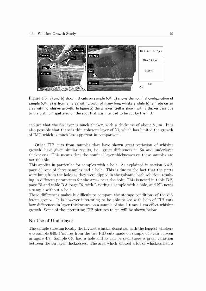
4.3. Whisker Growth Study 49
Figure 4.6: a) and b) show FIB cuts on sample 634, c) shows the nominal configuration of
sample 634. a) is from an area with growth of many long whiskers while b) is made on an
area with no whisker growth. In figure a) the whisker itself is shown with a thicker base due
to the platinum sputtered on the spot that was intended to be cut by the FIB.
can see that the Sn layer is much thicker, with a thickness of about 8 µm. It isalso possible that there is thin coherent layer of Ni, which has limited the growthof IMC which is much less apparent in comparison.
Other FIB cuts from samples that have shown great variation of whiskergrowth, have given similar results, i.e. great differences in Sn and underlayerthicknesses. This means that the nominal layer thicknesses on these samples arenot reliable.This applies in particular for samples with a hole. As explained in section 3.4.2,page 39, one of three samples had a hole. This is due to the fact that the partswere hung from the holes as they were dipped in the galvanic bath solution, result-ing in different parameters for the areas near the hole. This is noted in table B.2,page 75 and table B.3, page 76, with L noting a sample with a hole, and KL notesa sample without a hole.These differences makes it difficult to compare the storage conditions of the dif-ferent groups. It is however interesting to be able to see with help of FIB cutshow differences in layer thicknesses on a sample of size 1 times 1 cm effect whiskergrowth. Some of the interesting FIB pictures taken will be shown below
No Use of Underlayer
The sample showing locally the highest whisker densities, with the longest whiskerswas sample 640. Pictures from the two FIB cuts made on sample 640 can be seenin figure 4.7. Sample 640 had a hole and as can be seen there is great variationbetween the Sn layer thicknesses. The area which showed a lot of whiskers had a
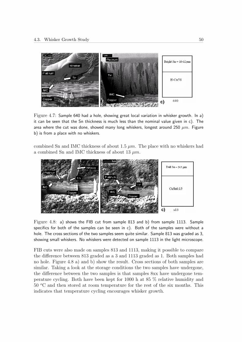
4.3. Whisker Growth Study 50
Figure 4.7: Sample 640 had a hole, showing great local variation in whisker growth. In a)
it can be seen that the Sn thickness is much less than the nominal value given in c). The
area where the cut was done, showed many long whiskers, longest around 250 µm. Figure
b) is from a place with no whiskers.
combined Sn and IMC thickness of about 1.5 µm. The place with no whiskers hada combined Sn and IMC thickness of about 13 µm.
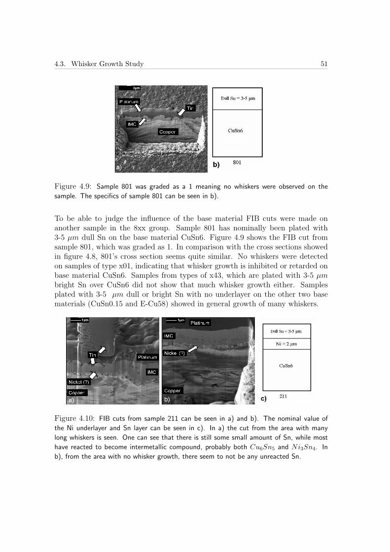
Figure 4.8: a) shows the FIB cut from sample 813 and b) from sample 1113. Sample
specifics for both of the samples can be seen in c). Both of the samples were without a
hole. The cross sections of the two samples seem quite similar. Sample 813 was graded as 3,
showing small whiskers. No whiskers were detected on sample 1113 in the light microscope.
FIB cuts were also made on samples 813 and 1113, making it possible to comparethe difference between 813 graded as a 3 and 1113 graded as 1. Both samples hadno hole. Figure 4.8 a) and b) show the result. Cross sections of both samples aresimilar. Taking a look at the storage conditions the two samples have undergone,the difference between the two samples is that samples 8xx have undergone tem-perature cycling. Both have been kept for 1000 h at 85 % relative humidity and50 oC and then stored at room temperature for the rest of the six months. Thisindicates that temperature cycling encourages whisker growth.
4.3. Whisker Growth Study 51
Figure 4.9: Sample 801 was graded as a 1 meaning no whiskers were observed on the
sample. The specifics of sample 801 can be seen in b).
To be able to judge the influence of the base material FIB cuts were made onanother sample in the 8xx group. Sample 801 has nominally been plated with3-5 µm dull Sn on the base material CuSn6. Figure 4.9 shows the FIB cut fromsample 801, which was graded as 1. In comparison with the cross sections showedin figure 4.8, 801’s cross section seems quite similar. No whiskers were detectedon samples of type x01, indicating that whisker growth is inhibited or retarded onbase material CuSn6. Samples from types of x43, which are plated with 3-5 µmbright Sn over CuSn6 did not show that much whisker growth either. Samplesplated with 3-5 µm dull or bright Sn with no underlayer on the other two basematerials (CuSn0.15 and E-Cu58) showed in general growth of many whiskers.
Figure 4.10: FIB cuts from sample 211 can be seen in a) and b). The nominal value of
the Ni underlayer and Sn layer can be seen in c). In a) the cut from the area with many
long whiskers is seen. One can see that there is still some small amount of Sn, while most
have reacted to become intermetallic compound, probably both Cu6Sn5 and Ni3Sn4. In
b), from the area with no whisker growth, there seem to not be any unreacted Sn.

4.3. Whisker Growth Study 52
Figure 4.11: In a) the EDX analysis over the FIB cut where there was a lot of whiskers
on sample 211. b) is from the place with no whiskers. As can be seen the presence of Ni
is more evident on the EDX analysis taken from the place with substantial whisker growth.
The cross section of the two FIB cuts can be seen in figure 4.10.
There has however been extensive whisker growth observed on some samples withbase material CuSn6, e.g. sample 211, which nominally has 2 µm Ni underlayerand 3-5 µm dull Sn and has been studied with FIB cuts as shown in followingsection.
Ni Underlayer
Some samples with holes with nominal Ni underlayer showed extensive whiskergrowth. Sample 211, which has a hole, was graded as 1-4 with the biggest whiskerbeing at least 120 µm. As mentioned the base material for 211 is CuSn6, a basematerial which has not shown that much whisker growth. Figure 4.10 shows thetwo cross sections done on the sample 211, a) from the area with high whiskerdensity and b) from the place with no whiskers. In b) there seems to be nounreacted Sn left and the layer that probably is the Ni layer (and not IMC) seemscoherent, otherwise there is not much difference between the two cross sections.EDX analysis made from the area of the cuts show some difference as seen infigure 4.11 a) and b). Presence of Ni is more evident in the EDX analysis takenfrom the area of the cuts over the place with a lot of whiskers. This indicates thatat least there is more Ni in the top layer for the whisker dense place.FIB cuts were also made on samples 138 and 335 which showed inhomogeneouswhisker growth. They have a nominal Ni layer thickness of 2 µm. The Ni layerobservable on these samples were less than that. It is however difficult to seeclearly were Ni layer ends and were IMC begins. Table 4.4 is a summary of themeasured Sn and IMC thickness of these samples.For samples without hole (presumably with more reliable layer thicknesses) and Niunderlayer there are only three samples showing whisker growth. These samples

4.3. Whisker Growth Study 53
Figure 4.12: The nominal values for samples 833, shown in a) and sample 1033 shown in
b) can be seen in c). Sample 1033 showed more and longer whiskers than sample 833.
are 821, 833 and 1033 with 0.2 µm Ni layer. FIB cuts were made on all thesesamples. The FIB cut showed that the Sn layer thickness on all these samplesis about 3 µm, which is according to the nominal values. Figure 4.12 shows theFIB cuts on samples 833 and 1033. Samples 821 and 833 were graded as 2-3,meaning that not many whiskers were detected on the two samples. Sample 1033was however graded as 4, with some whiskers longer than 80 µm. The differencebetween samples 821 and 833 and sample 1033 is that there is more IMC on 1033than the other two.
Ag Underlayer
Only two samples without hole and with Ag underlayer showed whisker growth.Figure 4.13 shows the FIB cuts made on these two samples, sample 1032 and 1120.The cross sections of the samples agree with the nominal layer thickness of both ofthe samples (2 µm Ag underlayer and 10-12 µm dull Sn layer). Sample 1032 hasthe base material E-Cu58 and sample 1120 has base material CuSn0.15. It has tobe noted that both samples showed little amount of whisker growth, the longestwhiskers noted had length of about 20 µm. It is however interesting to see that
138 211 335No whisker Whisker No whisker Whisker No whisker Whisker
Sn thickness [ µm ] 4.24 0.21 0 0.16 0 0.08IMC thickness [ µm ] 2.12 2.77 1.65 1.65 1.82 1.68Sn and IMCthickness [ µm ] 6.36 2.98 1.65 1.81 1.82 1.76
Table 4.4: Samples 138, 211 and 335 had a nominal Ni layer thickness of 2 µm. The Snand IMC thicknesses are measuered from the FIB cuts made on these samples.

4.3. Whisker Growth Study 54
Figure 4.13: The two pictures show FIB cut from samples 1032 and 1120. Both sample
1032, shown in a) and sample 1120 shown in b) had the nominal values of 10-12 µm dull
Sn plated on 2 µm Ag underlayer, which is in accordance with the thicknesses seen in the
figure.
there can be whisker growth despite a 2 µm Ag underlayer.
Sample Whisker volume Sn thickness IMC Sn+IMC IMC/(Sn+IMC)per area [nm] [µm] [µm] [µm]
138 0 4.24 2.12 6.36 0.33211 0 0 1.65 1.65 1.00335 0 0 1.82 1.82 1.00801 0 1.09 1.01 2.10 0.48640 0 11.57 1.04 12.61 0.08
1113 0.246 1.19 1.44 2.63 0.55211 0.653 0.16 1.65 1.81 0.91138 0.893 0.21 2.77 2.98 0.93833 2.40 2.47 0.33 2.80 0.12821 4.33 2.35 0.33 2.68 0.12335 4.69 0.08 1.68 1.76 0.95813 7.65 1.01 1.77 2.78 0.64640 21.2 0.42 1.07 1.49 0.72
Table 4.5: Whiskers around the FIB cuts were measuered and based on those measurementsthe whisker volume per unit length was calculated. Also from the pictures taken in the FIBsystem the thicknesses of the Sn layer and the IMC layer were measured.
Density Check
Whisker density check was done on some of the samples that were studied withFIB. The whisker densities of these samples are compared to the Sn and IMClayer thicknesses of the samples in table 4.5. There is little correlation to be notedbetween whisker growth and the other parameters listed in the table. It can be seen

4.3. Whisker Growth Study 55
that samples showing inhomogeneous whisker growth have either a much thickerSn layer where there is no whisker growth compared with where there is whiskers,or they do not have any unreacted Sn layer where there is no whisker growth.

Chapter 5
Discussion of the Results
In this chapter the experimental findings will be reviewed and compared with thetheoretical models and existing research.
5.1 Mechanical Properties
The calculations and the results achieved shows that Sn whiskers have high re-silience against vibration and mechanical shock. The risk of whiskers breaking offand causing a short somewhere else on the electronic board can however not beruled out based on our tests or calculations. It is probable that longer and thinnerwhiskers than those tested are more likely to break off for vibrations and shocksthat were tested.In our tests random vibrations were applied on the samples, which could meanthat the natural frequency of the whisker could be in the test frequency range butnot sustained long enough to make the whisker to break off. However, consideringthe second test with a duration of 22 hours, it is not likely that this was the case.This would mean that either the Young’s modulus made the natural frequency ofthe whiskers tested to be outside the tested frequency range or whiskers are notdamaged by vibrations in the range of their natural frequency.
5.2 Electrical Properties
It can be seen in table 4.2 that the resistivity of the different whiskers differ up toa factor of 100. This is thought to depend mostly on a thin isolating layer of oxidesurrounding the whisker. Another factor for the huge difference in the results isthe difference in the contact resistance.Two of the resistivity measured are lower than the resistivity given for β-Sn in theliterature. This could be perhaps because whiskers are single crystals and therefore
Nayeri Hashemzadeh, 2005. 56
5.3. Tin Whisker Growth 57
have lower resistivity.The highest current measured to be tolerated by a whisker was 55 mA. This valueis higher than what has been reported from other authors, e.g. Dunn 1988 [11].The peculiar graph shown in figure 4.4, where the measured current first goes upto 54 mA, than decreases to about 45 mA and thereafter goes to peak at 55 mA(the compliance current) is probably due to start of changes in the whisker, e.g.melting of the tip of the whisker.The FEM simulation of the critical current for different lengths of whiskers of witha diameter 2.5 µm was based on a small experimental data base. The simulation offusing temperature could become considerably better with a bigger experimentaldata base. The simplification of the environment of the whisker to be vacuum ispresumably more important when the whisker is longer, resulting in a lower criticalcurrent. However, the results give a good indication of the currents a whisker cantolerate, as well as how current carrying capacity depends on the length.
5.3 Tin Whisker Growth
The plating of the samples revealed to be inhomogeneous, especially in the regionsof the holes. Therefore the finding of clear correlations is very difficult. There arehowever some clear conclusions which can be drawn from the investigation of allthe samples with the light microscope. The results of this investigation is foundin table B.2 and table B.3. One clear result is that it is important to be able tocontrol the plating parameters to get a homogenous plating.
5.3.1 Heat Treatment
One of the results worth noting in table B.2, page 75 and table B.3, page 76, isthat samples that have been heat treated can grow whiskers, however the whiskergrowth observed was limited. Samples that had undergone heat treatment werekept at 180 oC for 5 minutes, which is a known mitigation practice (see section 2.3).Out of the 66 heat treated samples, 4 showed whisker growth after six month. Thelongest whisker measured (on sample 628) was around 25 µm. This indicates thatheat treatment restrains whisker growth.
5.3.2 Soldering Simulation
It can be seen from the light microscope investigation that reflow of the Sn platedsurface as a mitigation strategy (see section 2.3) is not effective. Groups 0xx to5xx underwent all soldering simulation (see table A.1, page 67), which is reflow ofthe Sn plated surface (that is heating the surface above the Sn melting point). As

5.3. Tin Whisker Growth 58
can be seen in table B.2 and table B.3 there is extensive whisker growth on someof these samples.
5.3.3 Storage Conditions
It is difficult to draw any clear conclusion from the storage conditions due to theuneven plating quality of the samples. The following conclusions are based on theFIB studies and due to the small quantity perhaps immature.FIB cuts made on samples 813 and 1113 (see figure 4.8, page 50) show that bothsamples had equivalent Sn layer thicknesses. Sample 813 showed whisker growthwhile no whisker growth was observed on sample 1113 in the light microscope. Areason behind this difference is perhaps that the 8xx group have undergone tem-perature cycling as opposed to the 11xx group (see the appendix A and table A.1).Figure 4.12 on page 53 show the FIB cuts on the samples 833 and 1033, whichshow equivalent Sn layer thicknesses. It is however impossible to judge if thenominal 0.2 µm Ni layer of the samples are equivalent. More whisker growth andlonger whiskers were observed on sample 1033. There is more IMC growth onsample 1033 than 833 according the pictures from the FIB system. If the Ni layerthicknesses of both samples are assumed to be equal, the more extensive whiskergrowth of sample 1033 could be contributed to the difference in storage conditions.Group 10xx has been stored at 50 oC while the group 8xx has been stored at roomtemperature. Group 8xx has also undergone temperature cycling, which group10xx has not (see table A.1, page 67).
5.3.4 Base Material
Looking at the three different base materials (see appendix A, table A.2, page 67for composition of the three base materials) samples with base material CuSn6showed less whisker growth than samples with the two other base materials. Acomparison of the observed whisker growth can be seen in table 5.1.
Samples with WhiskersBase Material No Hole All
CuSn6 4/107 20/176CuSn0,15 11/112 40/176
E-Cu58 10/111 40/176
Table 5.1: An overview is given of how many samples that showed whiskers in relation tothe base materials and if the samples had holes on them or not.
Looking at the samples without hole only four samples showed growth of whiskers
5.3. Tin Whisker Growth 59
on samples with base material CuSn6. The whiskers observed on three of thefour samples were smaller than 10 µm. The forth sample, sample 444, which wasgraded as 1-4 (a grading that indicates uneven plating) showed whiskers as longas 100 µm.Another aspect of samples with base material CuSn6 is that beside sample 442which had a hole, no whiskers were found on samples with the nominal 3-5 µm Snlayer and no underlayer. This was studied with a FIB cut made on sample 801(see figure 4.9, page 51), which showed a 1 µm thick IMC layer and 1 µm Sn layer.This is equivalent to the IMC and Sn layer seen in the FIB cuts made on sample813 (see figure 4.8, page 50). The Tu model which assumes the IMC growth as thereason behind whisker growth (see section 2.2.3) can not be confirmed with theseresults [26].There are however samples with base material CuSn6 showing growth of very longwhiskers, up to 120 µm. These samples have however a hole on them, whichsuggest uneven plating. A conclusion out of these results could be that the rangeof Sn thickness which within the whisker growth occurs on base material CuSn6is more narrow, with the upper limit of the Sn thickness being quite low (withregards from FIB cuts made on sample 801 lower than 2 µm).
5.3.5 Underlayer
Use of Ni or Ag underlayer seems to have a damping effect on whisker growth.However some of the longest whiskers that were found where on samples whichnominally had a Ni underlayer. Results from FIB cuts made on samples withwhisker growth showed that the Ni layer thickness on these samples were underthe nominal values. Three of the samples with Ni underlayer and no hole showedwhisker growth, and all these samples had nominally 0.2 µm Ni underlayer. Thiscould suggest that an intact 2 µm thick Ni underlayer prevents whisker growth.The few whiskers found on samples with Ag underlayer were all quite small. Judg-ing from the cross section pictures taken from these samples the layer thicknessesare according the nominal value. There is no IMC visible, which is another argu-ment against the model of Tu that assumes growth of IMC as the reason behindwhisker growth [26].Looking at the FIB cuts made on samples with Ag underlayer that showed whiskergrowth (see figure 4.13 a) and b) ) there is some interesting note to take. Eventhough the Sn layer is very thick on these samples, there is mostly no more thanone grain in the vertical direction. The picture taken from cross sections withthick Sn layer and no whisker growth however show several grains in the verticaldirection as can be seen in figure 4.6 b) and figure 4.7 b). This is in accordancewith the stored strain energy theory (see section 2.2.2, page 22) where the nor-mal recrystallization process is assumed to be inhibited due to grain boundary

5.3. Tin Whisker Growth 60
Figure 5.1: a) Illustration of figure 4.13 a) and b), where there is only one grain in the ver-
tical direction for the samples with Ag underlayer that showed whisker growth. b) illustrates
figures 4.6 b) and 4.7 b) which are pictures taken from places with no whisker growth. In
these pictures one can observe several grains in the vertical direction.
immobility. The boundaries would be pinned to there position, perpendicular tothe surface. Thereof thicker layers of Sn with more than one grain in the verti-cal direction would be less likely to show whisker growth. This is illustrated infigure 5.1.
5.3.6 Dull versus Bright Sn
The presented results do not indicate that bright Sn is more prone to whiskergrowth than dull Sn. The longest whiskers were however observed on sampleswith bright Sn.The mechanisms for whisker growth on bright Sn and dull Sn seem to differ onsome manners. The grains of bright Sn are usually too small in their normal sizeto support a whisker, therefore whiskers on bright Sn seem to mostly grow from anodule or with following flower eruptions as can be seen in figure 2.2 and figure 4.7.This growth mechanism demands a more complex explanation for whisker growthon bright Sn than dull Sn.
5.3.7 Tin Layer Thickness
Table 4.5 is a trial to find a relation between Sn layer thickness and IMC growthwith whisker growth. The information about the IMC and Sn thickness was takenfrom the FIB cuts. Another problem that should be noted is that some of thesamples had Ni underlayer and some of the IMC formed would be between Sn andNi. The differences between bright and dull Sn has not been taken in considerationeither. With all these objections it is interesting to see that there is very little con-

5.3. Tin Whisker Growth 61
nection between the parameters put up and whisker growth. What can be seen isthat samples showing inhomogeneous whisker growth, have either a much thickerSn layer on the areas where there is no whisker growth compared with where thereis whiskers, or they do not have any unreacted Sn layer on the areas where thereis no whisker growth. This indicates that whisker growth in relation with the Snlayer thickness occurs within an interval as written in section 2.3. These intervalsseem to depend strongly on the base material, underlayer, the storage conditionsand type of Sn (dull or bright Sn). At the same time a limit is maybe a to definiteanswer to a problem which is more complex than that.
5.3.8 Conclusions on Whisker Growth Models
Whisker growth as a result of surface energy effects (see section 2.2.1) seem tolack in ability to explain why whisker growth differs for Sn plated on different basematerials as well as the role of the Sn layer thickness on whisker growth. Thesuccess of different mitigation strategies, e.g. annealing or use of underlayer is nottreated in the proposed models either.Tu’s model where whisker growth is explained due to internal mechanical stresscaused by growth of the IMC Cu6Sn5 (see section 2.2.3) is incompatible with someof the findings done in this work. These findings are lack of clear correlation be-tween IMC thickness and whisker growth and that whisker growth was observedon samples with Ag underlayer despite lack of IMC.Stored strain energy where an abnormal recrystallization process is behind whiskergrowth (see chapter 2.2.2) seems not to be contradicted by this work. However,reasons behind why whisker growth would differ on different base material or withuse of underlayer are not treated in the literature that was studied [24, 25].

Chapter 6
Future Work
For the electronic industry there is still a lot of work to be done to be able torely on Sn coatings. Due to the urgent necessity of attending to the Sn whiskergrowth problem, work on whisker growth will have to go in two directions. Oneis to understand in detail the complex mechanisms of whisker growth. The otheris to decide on which remedies that can restrain whisker growth. Solutions thatprovide enough security against failures while not adding to much new costs andsteps to the production. Remedies on this problem will perhaps come beforethe whisker growth mechanisms are fully understood. This could be achieved bychanging parameters such as base material, underlayer, Sn layer thickness as wellas experimenting on the preparation conditions, from changing the galvanic bathproperties to post treatment after the plating.When it comes to the work that has been done in this thesis, it will be interestingto follow up on the samples that were studied to see how they have evolved. Itwould also be interesting to investigate the actual layer thicknesses and perhapsthis way being able to decide more accurate the parameters that will restrainwhisker growth.
Nayeri Hashemzadeh, 2005. 62

Bibliography
[1] B. D. Dunn, Whisker Formation on Electronic Materials, Circuit World, 2,4, pp. 32-40, (1976).
[2] G. T. Galyon, Annotated Tin Whisker Bibliography, NEMI Tin WhiskerModeling Project, (July 2003).
[3] H. L. Cobb, Cadmium Whiskers, The Monthly Review of the AmericanElectroplaters Society, 33, pp. 28-30, (1946).
[4] I. Amato, Tin Whiskers: The Next Y2K Problem?,Available on: http://www.fortune.com/fortune/thisjustin/0,15704,1012859,00.html,Fortune Magazine, (Jan, 2005).
[5] J. A. Brusse, G. J. Ewell, J. P. Siplon, Tin Whiskers: Attributes and Mitiga-tion, 22nd Capacitor and Resistor Technology Symposium, pp. 67-80, (2002).
[6] B. D. Dunn, Metallurgy and Reliability in Spacecraft Electronics, Metals andMaterials, 34, pp. 32-40, (1975).
[7] K. M. Cunningham, M. P. Donahue, Tin Whiskers: Mechanism of Growthand Prevention, 4th International SAMPE Electronics Conference,pp. 569-575, (1990).
[8] C. Herring, J. K. Galt, Elastic and Plastic Properties of Very Small MetalSpecimens, Letters to the Editor, pp. 1060-1061, (1952).
[9] C. Kittel, Introduction to Solid State Physics, Seventh Edition, pp. 587-607,(1996).
[10] G. T. T. Sheng, C. F. Hu, W. J. Choi, K. N. Tu, Y. Y. Bong, L. Nguyen, TinWhiskers Studied by Focused Ion Beam Imaging and Transmission ElectronMicroscopy, Journal of Applied Physics, 92, 1, pp. 64-69, (2002).
[11] B. D. Dunn, Mechanical and Electrical Characteristics of Tin Whiskers withSpecial Reference to Spacecraft Systems, European Space Agency, (1988).
Nayeri Hashemzadeh, 2005. 63

Bibliography 64
[12] H. P. Kehrer, H. G. Kadereit, Tracer Experiments on the Growth of TinWhiskers, Appleid Physics Letters, 16, 11, pp. 411-412, (1970).
[13] S. E. Koonce, S. M. Arnold, Growth of Metal Whiskers, Letters to the Editor,pp. 365-366, (1952).
[14] M. O. Peach, Mechanism of Growth of Whiskers on Cadmium, Letters to theEditor, pp. 1401-1403, (1952).
[15] R. M. Fisher, L. S. Darken, K. G. Carroll, Accelerated Growth of ThinWhiskers, Acta Metallurgica, 2, (1954).
[16] C. Nordling, J. Osterman, Physics Handbook for Science and Engineering,Studentlitteratur, (1999).
[17] http://www.webelements.com, (Jan, 2005).
[18] T. B. Massalski, Binary Alloy Phase Diagrams, pp. 964-965.
[19] K. N. Tu, Interdiffusion and Reaction in Bimetallic Cu-Sn Thin Films, ActaMetallurgica, 21, pp. 347-354, (1973).
[20] G. T. Galyon, A History of Tin Whisker Theory: 1946 to 2004, IBM eSGGroup, (2004).
[21] J. D. Eshelby, A Tentative Theory of Metallic Whisker Growth, Journal ofApplied Physics, pp.755-756, (1953).
[22] F. C. Frank, On Tin Whiskers, Philosophical Magazine, 44, pp. 854-860,(1953).
[23] W. C. Ellis, D. F. Gibbons, R. C. Treuting, Growth of Metal Whiskers Fromthe Solid, John Wiley& Sons, pp. 102-120, (1958).
[24] N. Furuta, K. Hamamura, Growth Mechanism of Proper Tin- Whisker,Japanese Journal of Applied Physics, 8, 12, pp. 1404-1410, (1969).
[25] I. Boguslavsky, P. Bush, Recrystallization Principles Applied to WhiskerGrowth in Tin, APEX Conference, (2003).
[26] K. N. Tu, Irreversible Process of Spontaneous Whisker Growth in BimetallicCu-Sn Thin Film Reactions, Physical Review B, 49, 3, pp. 2030-2034, (1994).
[27] M. W. Barsoum, E. N. Hoffman,l R. D. Doherty, S. Gupta, A. Zavalian-gos, Driving force and Mechanism for Spontaneous Metal Whisker Forma-tion, Physical Review Letters, 93, 20, (2004).
Bibliography 65
[28] A. Zangwill, Pysics at Surfaces, Cambridge University Press, (2001).
[29] B. F. Dyson, T. R. Anthony, D. Turnbull, Interstitial Diffusion of Copper inTin, Journal of Applied Physics, 38, 8, p. 3408, (1967).
[30] D. Hull, D. J. Bacon, Introduction to Dislocations, Pergamon Press, 3rdEdition, (1984).
[31] C. M. Rice, D. S. Eppelsheimer, M. B. McNeil, Surface Tension of Solid Tin,Journal of Applied Physics, 37, 13, pp. 4766-4768, (1966).
[32] T. J. Whalen, S. M. Kaufman, Comment on ”Surface Tension of Solid Tin”by Rice, Eppelsheimer, and McNeil, Journal of Applied Physics, 38, 8, pp.3408-3409, (1967).
[33] U. Lindborg, A Model for the Spontaneous Growth of Zinc, Cadmium andTin Whiskers, Acta Metallurgica, 24, pp. 181-186, (1976).
[34] P. Shewmon, Diffusion in Solids, The Minerals, Metals & Materials Society,Second Edition, (1989).
[35] U. Lindborg, Observations on the Growth of Whisker Crystals From Zn Elec-torplate, Metallurgical Transactions, 6A, 8, pp. 1581-1586, (1975).
[36] D. B. Butrymowicz, J. R. Manning, M. E. Read, Diffusion Rate and MassTransport Phenomena for Copper Systems, Natl. Bur. Stand (U.S.), (1977).
[37] R. J. Fields, S. R. Low, Physical and Mechanical Properties of Inter-metallic Compound Commonly Found in Solder Joints, Available on:http://www.metallurgy.nist.gov/mechanical properties/solder paper.html,(Mars, 2005).
[38] J. S. Kadesch, J. Brusse, The Continuing Dangers of Tin Whiskersand Attempts to Control them with Conformal Coating, Avail-able on: http://nepp.nasa.gov/docuploads/95565195-0E5A-40D8-98D88425FF668F68/JayBrusseRevision2.pdf, (Mars, 2005).
[39] M. Guber, Whiskerbildung im System Kupfer-Zinn, Max-Planck Institut furMetallforschnung Stuttgart, (2004).
[40] V. K. Glazunova, An Investigation of teh Conditions of Spontaneous Growthof Filiform Crystals on Electrolytic Coatings, translated from Zhurnal Prik-ladnoi Khimii, 36, 3, pp. 543-550, (1963).

Bibliography 66
[41] S. M. Arnold, Repressing the Growth of Tin Whiskers, Plating, 53, 1, pp.96-99, (1966).
[42] R. Schetty, Minimization of Tin Whisker Formation for Lead-Free ElectronicsFinishing, Circuit World, pp. 17-20, (2000).
[43] B. D. Dunn, A Laboratory Study of Tin Whisker Growth, European SpaceAgency, (1987).
[44] C. Xu, Y. Zhang, C. Fan, A. Vysotskaya, J. Abys, Understanding WhiskerPhenomenon-Mechanisms Study, Lucent Technologies, (2002).
[45] N. A. J. Sabbagh, H. J. McQueen, Tin Whiskers: Causes and Remedies,Metal Finishing, pp. 27-32, (1975).
[46] P. E. J. Flewitt, R. K. Wild, Physical Methods for Materials Characterisation,Institute of Physics Publishing, (2002).
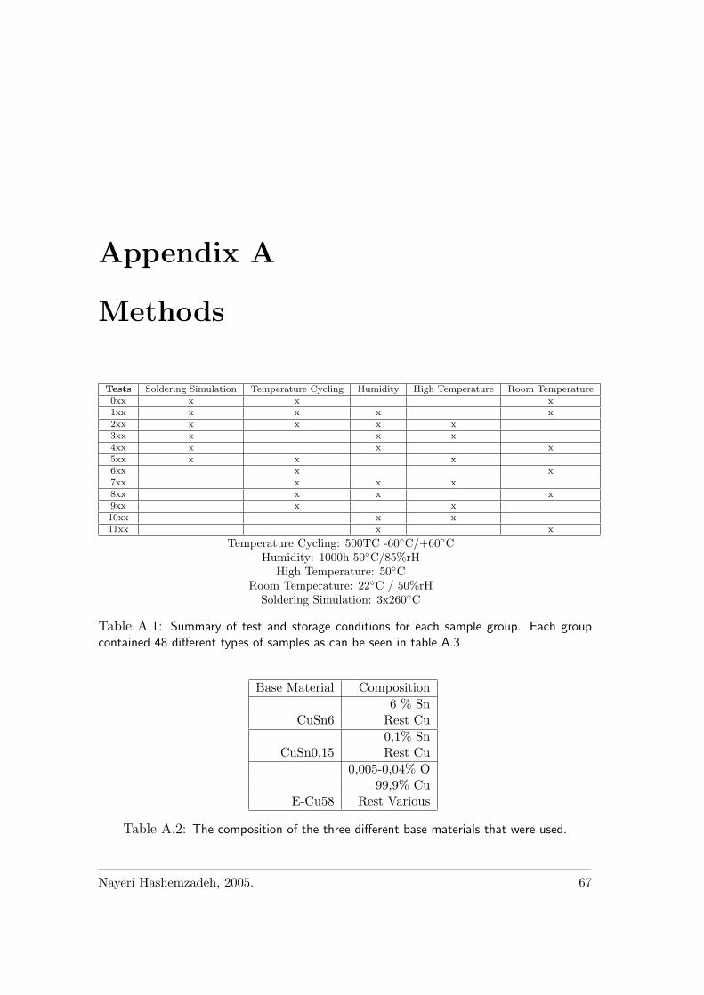
Appendix A
Methods
Tests Soldering Simulation Temperature Cycling Humidity High Temperature Room Temperature0xx x x x1xx x x x x2xx x x x x3xx x x x4xx x x x5xx x x x6xx x x7xx x x x8xx x x x9xx x x10xx x x11xx x x
Temperature Cycling: 500TC -60C/+60CHumidity: 1000h 50C/85%rH
High Temperature: 50CRoom Temperature: 22C / 50%rH
Soldering Simulation: 3x260C
Table A.1: Summary of test and storage conditions for each sample group. Each groupcontained 48 different types of samples as can be seen in table A.3.
Base Material Composition6 % Sn
CuSn6 Rest Cu0,1% Sn
CuSn0,15 Rest Cu0,005-0,04% O
99,9% CuE-Cu58 Rest Various
Table A.2: The composition of the three different base materials that were used.
Nayeri Hashemzadeh, 2005. 67
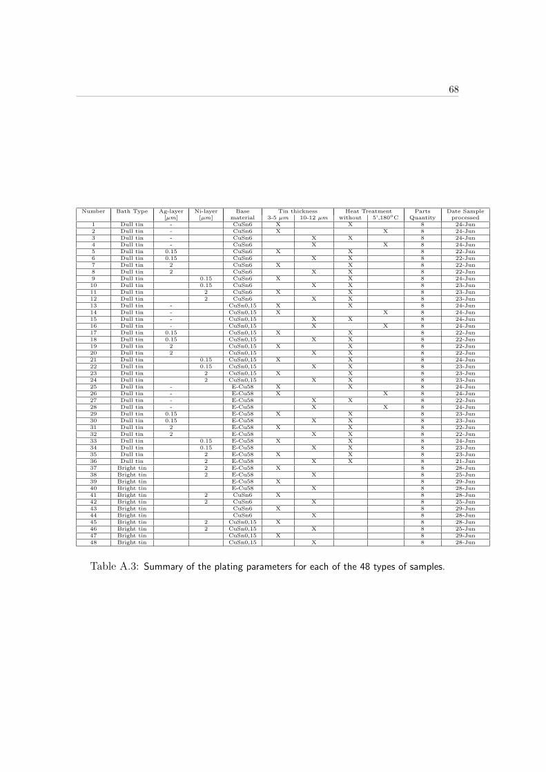
68
Number Bath Type Ag-layer Ni-layer Base Tin thickness Heat Treatment Parts Date Sample[µm] [µm] material 3-5 µm 10-12 µm without 5’,180oC Quantity processed
1 Dull tin - CuSn6 X X 8 24-Jun2 Dull tin - CuSn6 X X 8 24-Jun3 Dull tin - CuSn6 X X 8 24-Jun4 Dull tin - CuSn6 X X 8 24-Jun5 Dull tin 0.15 CuSn6 X X 8 22-Jun6 Dull tin 0.15 CuSn6 X X 8 22-Jun7 Dull tin 2 CuSn6 X X 8 22-Jun8 Dull tin 2 CuSn6 X X 8 22-Jun9 Dull tin 0.15 CuSn6 X X 8 24-Jun10 Dull tin 0.15 CuSn6 X X 8 23-Jun11 Dull tin 2 CuSn6 X X 8 23-Jun12 Dull tin 2 CuSn6 X X 8 23-Jun13 Dull tin - CuSn0,15 X X 8 24-Jun14 Dull tin - CuSn0,15 X X 8 24-Jun15 Dull tin - CuSn0,15 X X 8 24-Jun16 Dull tin - CuSn0,15 X X 8 24-Jun17 Dull tin 0.15 CuSn0,15 X X 8 22-Jun18 Dull tin 0.15 CuSn0,15 X X 8 22-Jun19 Dull tin 2 CuSn0,15 X X 8 22-Jun20 Dull tin 2 CuSn0,15 X X 8 22-Jun21 Dull tin 0.15 CuSn0,15 X X 8 24-Jun22 Dull tin 0.15 CuSn0,15 X X 8 23-Jun23 Dull tin 2 CuSn0,15 X X 8 23-Jun24 Dull tin 2 CuSn0,15 X X 8 23-Jun25 Dull tin - E-Cu58 X X 8 24-Jun26 Dull tin - E-Cu58 X X 8 24-Jun27 Dull tin - E-Cu58 X X 8 22-Jun28 Dull tin - E-Cu58 X X 8 24-Jun29 Dull tin 0.15 E-Cu58 X X 8 23-Jun30 Dull tin 0.15 E-Cu58 X X 8 23-Jun31 Dull tin 2 E-Cu58 X X 8 22-Jun32 Dull tin 2 E-Cu58 X X 8 22-Jun33 Dull tin 0.15 E-Cu58 X X 8 24-Jun34 Dull tin 0.15 E-Cu58 X X 8 23-Jun35 Dull tin 2 E-Cu58 X X 8 23-Jun36 Dull tin 2 E-Cu58 X X 8 21-Jun37 Bright tin 2 E-Cu58 X 8 28-Jun38 Bright tin 2 E-Cu58 X 8 25-Jun39 Bright tin E-Cu58 X 8 29-Jun40 Bright tin E-Cu58 X 8 28-Jun41 Bright tin 2 CuSn6 X 8 28-Jun42 Bright tin 2 CuSn6 X 8 25-Jun43 Bright tin CuSn6 X 8 29-Jun44 Bright tin CuSn6 X 8 28-Jun45 Bright tin 2 CuSn0,15 X 8 28-Jun46 Bright tin 2 CuSn0,15 X 8 25-Jun47 Bright tin CuSn0,15 X 8 29-Jun48 Bright tin CuSn0,15 X 8 28-Jun
Table A.3: Summary of the plating parameters for each of the 48 types of samples.

69
Process Step Time Temp. Current/ Thickness andVoltage/CD Other Data
Alkaline soak 30 sec. 60 oC NAElectro-Clean 60 sec. 65 oC 8.0 V
Cleaner 5 sec. 25 oC. NANeutralization
Activation 30 sec. 25 oC NA
0.15 and 2µm as
requiredNickel Plating 120 sec. 55 oC 5 A/dm2 (see test
matrix)
0.15 and 2Silver barrier 10 sec. 25 oC at 5 A/dm2 µm aslayer plating 154 sec. required
(see matrix)
3-5 µm andTin Plating-1 140 sec. 45 oC 20 A/dm2 10-12 µm
(dull tin) 32 sec. as requiered(see matrix)
3-5 µm andTin Plating-2 165. Sec 40 oC 20 A/dm2 10-12 µm(bright tin) as requiered
48 sec. (see matrix)
Rinse 5 sec. 25 oC NAPost- 10 sec. 25 oC NA
Treatment-1Rinse 10 sec. 60 oC NAPost- 10 sec. 25 oC NA
Treatment-2Rinse 10 sec. 25 oC NA Followede by
hot air dry
Table A.4: Plating protocol for the samples used to study whisker growth under differentstorage conditions.
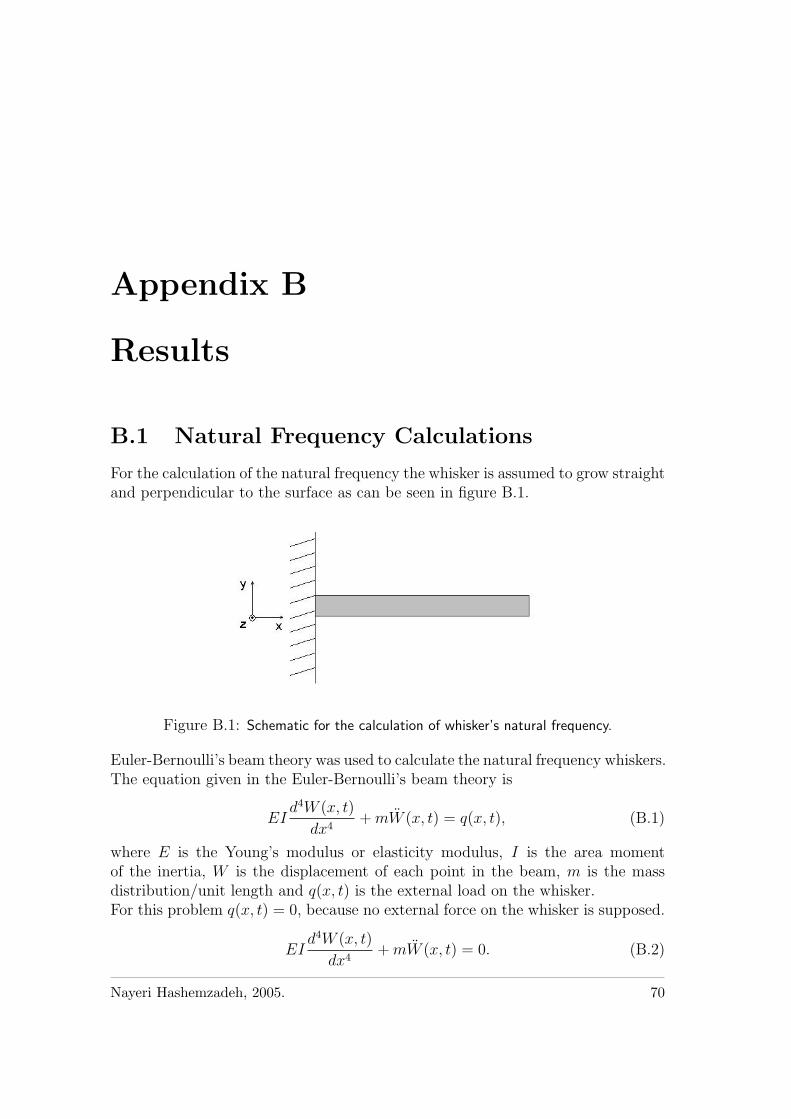
Appendix B
Results
B.1 Natural Frequency Calculations
For the calculation of the natural frequency the whisker is assumed to grow straightand perpendicular to the surface as can be seen in figure B.1.
Figure B.1: Schematic for the calculation of whisker’s natural frequency.
Euler-Bernoulli’s beam theory was used to calculate the natural frequency whiskers.The equation given in the Euler-Bernoulli’s beam theory is
EId4W (x, t)
dx4+ mW (x, t) = q(x, t), (B.1)
where E is the Young’s modulus or elasticity modulus, I is the area momentof the inertia, W is the displacement of each point in the beam, m is the massdistribution/unit length and q(x, t) is the external load on the whisker.For this problem q(x, t) = 0, because no external force on the whisker is supposed.
EId4W (x, t)
dx4+ mW (x, t) = 0. (B.2)
Nayeri Hashemzadeh, 2005. 70
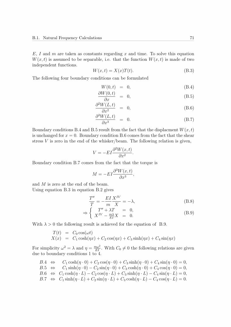
B.1. Natural Frequency Calculations 71
E, I and m are taken as constants regarding x and time. To solve this equationW (x, t) is assumed to be separable, i.e. that the function W (x, t) is made of twoindependent functions.
W (x, t) = X(x)T (t). (B.3)
The following four boundary conditions can be formulated
W (0, t) = 0, (B.4)
∂W (0, t)
∂x= 0, (B.5)
∂2W (L, t)
∂x2= 0, (B.6)
∂3W (L, t)
∂x3= 0. (B.7)
Boundary conditions B.4 and B.5 result from the fact that the displacment W (x, t)is unchanged for x = 0. Boundary condition B.6 comes from the fact that the shearstress V is zero in the end of the whisker/beam. The following relation is given,
V = −EI∂2W (x, t)
∂x2.
Boundary condition B.7 comes from the fact that the torque is
M = −EI∂3W (x, t)
∂x3,
and M is zero at the end of the beam.Using equation B.3 in equation B.2 gives
T ′′
T= −EI
m
XIV
X= −λ, (B.8)
⇒
T ′′ + λT = 0,XIV − mλ
EIX = 0.
(B.9)
With λ > 0 the following result is achieved for the equation of B.9.
T (t) = C0 cos(ωt)X(x) = C1 cosh(ηx) + C2 cos(ηx) + C3 sinh(ηx) + C4 sin(ηx)
For simplicity ω2 = λ and η = mω2
EI. With C0 6= 0 the following relations are given
due to boundary conditions 1 to 4.
B.4 ⇔ C1 cosh(η · 0) + C2 cos(η · 0) + C3 sinh(η · 0) + C4 sin(η · 0) = 0,B.5 ⇔ C1 sinh(η · 0)− C2 sin(η · 0) + C3 cosh(η · 0) + C4 cos(η · 0) = 0,B.6 ⇔ C1 cosh(η · L)− C2 cos(η · L) + C3 sinh(η · L)− C4 sin(η · L) = 0,B.7 ⇔ C1 sinh(η · L) + C2 sin(η · L) + C3 cosh(η · L)− C4 cos(η · L) = 0.

B.1. Natural Frequency Calculations 72
Boundary conditions B.4 and B.5 result in C2 = −C1 and C4 = −C3. Boundaryconditions B.6 and B.7 result in the following equation matrix.(
cosh(η · L) + cos(η · L) sinh(η · L) + sin(η · L)sinh(η · L)− sin(η · L) cosh(η · L) + cos(η · L)
) (C1
C3
)=
(00
).
For this equation system to have a non trivial solution the determinant of it shouldbe equal to zero. That is∣∣∣∣ cosh(η · L) + cos(η · L) sinh(η · L) + sin(η · L)
sinh(η · L)− sin(η · L) cosh(η · L) + cos(η · L)
∣∣∣∣ = 0.
This givescosh(η · L) cos(η · L) + 1 = 0. (B.10)
This equation gives the natural frequency of the whisker/beam. ω substitutedback instead of η into equation (B.10) gives:
cosh((m
EI)1/4L
√ω) cos((
m
EI)1/4L
√ω) + 1 = 0.
This equation can be solved numerically, e.g. by using Matlab. Figure B.2 showshow this function looks like up to the first mode. Here x = ( m
EI)1/4L
√ω. This
Figure B.2: Plot over equation B.10, where first zero occurs for x = 1.88.
function has infinite amount of zeros, due to the cos in the function. Only the firstzero point is interesting due to the high natural frequencies of the whiskers. Thefirst zero for the function is for x = 1.88. This gives
f =ω
2π=
1
2π(EI
m)1/2(
1.88
L)2 (B.11)
B.1. Natural Frequency Calculations 73
The area moment of the inertia is calculated in the following way
I =
∫ ∫y2dydz (B.12)
The area moment of the inertia for a cylinder is I = πd4
64, where d is the diameter
of the whisker. The mass per unit length of the whiskers, m = πρ(d2)2 · 1, where 1
is the unit length and ρ is the density of the whisker. Putting these substitutionsinto equation B.11 result in
f =1
2π
√√√√E · (πd4
64)
(πρd2
4)
(1.88
L)2 (B.13)
⇔ f =1.882
8π√
ρ
√Ed
L2(B.14)
B.1.1 Connected at Both Ends
For a whisker that is connected at both ends the boundary conditions are differ-ent. Presuming that the connections at both ends are equal, following boundaryconditions are valid
W (0, t) = 0, (B.15)
∂W (0, t)
∂x= 0, (B.16)
W (L, t) = 0, (B.17)
∂W (L, t)
∂x= 0. (B.18)
Following the same procedure as the case with one end free the following equationis achieved
cosh(η · L) cos(η · L)− 1 = 0. (B.19)
The first solution of equation B.19 is η · L = 4.73 instead of 1.88 for the one endfree case. Comparing equation B.11 the natural frequency of whiskers connected
at both ends is(
4.731.88
)2= 6.36 times higher.
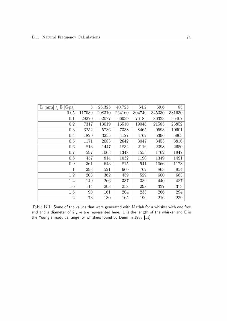
B.1. Natural Frequency Calculations 74
L [mm] \ E [Gpa] 8 25.325 40.725 54.2 69.6 850.05 117080 208310 264160 304740 345330 3816300.1 29270 52077 66039 76185 86333 954070.2 7317 13019 16510 19046 21583 238520.3 3252 5786 7338 8465 9593 106010.4 1829 3255 4127 4762 5396 59630.5 1171 2083 2642 3047 3453 38160.6 813 1447 1834 2116 2398 26500.7 597 1063 1348 1555 1762 19470.8 457 814 1032 1190 1349 14910.9 361 643 815 941 1066 1178
1 293 521 660 762 863 9541.2 203 362 459 529 600 6631.4 149 266 337 389 440 4871.6 114 203 258 298 337 3731.8 90 161 204 235 266 294
2 73 130 165 190 216 239
Table B.1: Some of the values that were generated with Matlab for a whisker with one freeend and a diameter of 2 µm are represented here. L is the length of the whisker and E isthe Young’s modulus range for whiskers found by Dunn in 1988 [11].

B.1. Natural Frequency Calculations 75
”+” 0 100 200 300 400 5001 1–2, L 1; KL 1; KL 2; K 1–2; KL 1; L2 1, L 1; KL 2; KL 1; L 1; KL 1; KL3 1, L 1–2; KL 2; KL 2; KL 1; L 1–2; KL4 1, L 2; L 2; KL 2; KL (6 µm) 1–2; KL 1; L5 1, KL 1–2; KL 2; KL 1; L 1–2; KL 1; KL6 1, L 1; L 2; KL 1–2; ; KL 1; KL 1; KL7 1, Kl 2; L 1; KL 1–2; KL 1; L 1; KL8 1, L 1; KL 2; KL 1–2; KL 1–2; KL 1; L9 (65 µm) 3–4, L 1; KL 1; KL (10µm) 2–3; L 1; KL 1; KL
10 1, Kl 1–2; L 1; KL 1; L 1–2; KL 1; KL11 1, Kl 1; KL (120µm) 1-4; L (20 µm) 3–4; L 1; KL 1; KL12 1, L 2 ;L 1; KL 1–2; L 1; KL 2; KL13 (10 µm) 3, L (12 µm) 2–3; KL 1–2; KL (10 µm) 2–3; L (7 µm) 2; KL (20µm) 2-3; KL14 1, KL 1; L 1; KL 1; L 1; KL 1; KL15 1, KL 1; L 1; KL (10 µm) 3; L 1; KL 1; KL16 1, KL 1; L 1; KL 2; L 1–2; KL 1; KL17 1, KL ; L 1; KL 1–2; L 1–2; KL 1; KL18 1, KL 1–2; L 2; KL 2, L 1; KL 1–2; KL19 1, L 1; KL 1; KL 1; l 1; KL 1; KL20 1, KL 1; KL 1; L 2, l 1; KL 1; KL21 1, KL 1; L 1–2; KL 1–2, KL 1–2; KL (5µm) 2; L22 (55 µm) 3–4, L 1–2; KL 1; KL (15 µm) 3–4; L 1–2; KL 1; KL23 1, KL (3 µm) 1–3; L 1; KL (45 µm) 3–4; L 1; KL 1; KL24 1, L 1–2; KL 2; KL 2; L 1–2; KL 1; KL25 (50 µm) 4, KL 2–3; L (30 µm) 3; KL (10 µm) 3; L (15 µm) 2; KL 1; KL26 1, KL 1; L 1; KL 1–2; L 1; KL 1; KL27 1, L 1–2; KL 1; KL 2; L 1; KL 1; KL28 1, L 1; KL 1; KL 1–2; L 1; KL 1; KL29 1, L 1–2; KL 1; KL 2; L 1; KL 1; KL30 1; KL ; L 2; KL 1–2; L 1; KL 1; KL31 1, KL (8 µm) 1–3; L 1; KL 1–2; L 1; KL 1; KL32 1; KL 1–2; L 1 ; KL 1; L 1; KL 1; KL33 1; KL (5 µm) 1–3; L 1; KL (15 µm) 3; L 1; KL 1; KL34 1; KL (15µm) 3–4; L 1; KL (35 µm) 4; L 1; KL 1; KL35 1; KL (35 µm) 1–4; L 2-3; KL (110 µm) 1–5; L 1; KL 1; KL36 1; KL 1; L 1; KL 1–2; L 1–2; KL 1; KL37 1 ; KL (40µm) 1–4; L 1; KL (15 µm) 3; L 1–2; KL 1; KL38 1; KL (30 µm) 1–4, L 1; KL (30 µm) 1–4; L 1–2; KL 2; KL39 1; KL 1; L 1; KL (80 µm) 4; L (7 µm) 2; KL 1; KL40 1; KL (50 µm) 2–3; L 1–2; KL 1; L 1; KL 1; KL41 1; KL 1; L 1; KL (50 µm) 4; L (5µm) 1–2; KL 1; KL42 1; KL 1; L 1; KL 1–2; KL (80 µm) 1–4; L 1; KL43 1; L 1; KL 1; KL 1–2; L 1; KL 1; KL44 1; KL 1; L 1;KL 1–2; KL (100 µm) 1–4; KL 1; KL45 1; KL (140 µm) 1–4; L 1; KL (190 µm) 5; L 1; KL 1; KL46 1; L 1–2; KL 1; KL 1–2; L 1–2; KL 1; KL47 1; KL 1–2; KL 1; L 1–2; L (50 µm) 1–3; KL 1; KL48 1; KL (35 µm) 1–3; L 1; KL (70µm) 2–3; L 1–2; KL 1; KL
Table B.2: Results from studying whisker growth on different sets of samples undergoingdifferent storage conditions. In table A.3 and table A.1 sample properties and treatmentconditions for each sample can be found. The grading system is explained in table 3.2on page 40. The samples graded with two numbers show inhomogenous whisker growth.The longest whiskers measured on the sample are noted in paranthesis next to the grades.Samples with a hole are indicated with L and those without with KL.
B.1. Natural Frequency Calculations 76
”+” 600 700 800 900 1000 11001 1, L 1 1; KL 2; L 1; KL 1–2; KL2 1, L 1 1; KL 2; L 1; KL 1–2; KL3 1, L 1–2 1; KL 2; L 2; KL 1; KL4 1, L 1–2 1; KL 2; L 2; KL 1; KL5 1, L 1 1; KL 2; L 1; KL 1; KL6 1, L 1; KL (15 µm) 2–3; L 2; KL 1; KL7 1, L 1 1; KL 1–2; L 1; KL 1; KL8 1, L 1–3 1; KL (15 µm) 3; L 2; KL (5 µm) 2; KL9 (10 µm) 2–3, L 1–2; KL 1; L 1; KL 1; KL
10 (50 µm) 3–4, L 1; KL (10 µm) 2–3; L 1; KL 1; KL11 1–2, L 1–2; KL 1; L 1; KL 1–2; KL12 (7 µm) 1–3, L 1–2; KL 1; L 1; KL 1–2; KL13 (30 µm) 4, L (20µm) 3; KL (15 µm) 3; L (10 µm) 3; KL 1; KL14 2, L 1; KL 1; L 1; KL 1; KL15 (30 µm) 2–3, L 1; KL 2; L 2; KL (5 µm) 1–2; KL16 1, L 1–2; KL 2–3; L 2; KL 1; KL17 1, L 1; KL 1; L 1; KL 1; KL18 (20 µm) 2–3, L 1; KL (30 µm) 3; L 1; KL 1; KL19 1, L 1; KL 2; L 1; KL 1; KL20 (30 µm) 3, L 1; KL (15 µm) 2–3; L 2; KL (9 µm) 2; KL21 (30 µm) 3–4, L (30µm) 2–3; KL (40 µm) 3–4; L 2; KL 1; KL22 (50 µm) 3–4, L 1; KL (10 µm) 2–3; L 1; KL 1–2; KL23 (10 µm) 2–3; L 1–2; KL (15 µm) 3; L 1; KL 1; KL24 (40 µm) 2–3; L 1; KL 2–3; L 1; KL 1; KL25 (25 µm) 2–3; L (6µm) 2; KL (15 µm) 3–4; L 2; KL 2; KL26 1–2; L (5µm) 2; KL 1; L 1; KL 1; KL27 (10 µm) 2–3; L 1; KL 2; L 1; KL 1; KL28 (25 µm) 2–3; L 1; KL 2–3; L 1; KL 1–2; KL29 1; L 1–2; KL 1; L 2; KL 1; KL30 (30 µm) 2–3; L 1–2; KL (35 µm) 2–3; L 1; KL 1; KL31 (20 µm) 2–3; L 1–2; KL 1; L 1; KL 1; KL32 1–2; L 1–2; KL 2; L (22 µm) 2–3; KL 1–2; KL33 (110 µm) 4; L (15µm) 2–3; KL (40 µm) 4; L (80 µm) 4; KL 1; KL34 (130 µm) 1–5; L 1; KL (40 µm) 3; L 2; KL 1; KL35 (25 µm) 1–3; L 1; KL 2; L 1; KL 1; KL36 2; L 1–2; KL 1; L 2; KL 1; KL37 1; L 1; KL 1; L 1–2; KL 1; KL38 1–2; L 1; KL 1; L 1; KL 1; KL39 (25 µm) 3; L 1–2; KL (130 µm) 1–5; L (50 µm) 3; KL (60 µm) 2–3; KL40 (250 µm) 1–5; L 1–2; KL (110 µm)1–5; L 1; KL 1–2; KL41 1; L 1; KL 1; L 1; KL 1; KL42 1; L ; KL 2; L 1; KL 1; KL43 (25 µm) 2–3; L 1–2; KL 1; L 1; KL 1; KL44 (25 µm) 2–3; L 1; KL 1; L 1; KL 1–2; KL45 1; L 1; KL 1; L 1; KL 1; KL46 1; L 1; KL 1; L 1; KL 1; KL47 (60 µm) 2–3; L (50µm) 1–3; KL 2; L 1–2; KL (40 µm) 2–3; KL48 (215 µm) 1–5; L 1; KL (110 µm) 1–5; L 1; KL 1–2; KL
Table B.3: See explenations for table B.2.

Copyright
The publishers will keep this document online on the Internet - or its possiblereplacement - for a period of 25 years from the date of publication barring excep-tional circumstances. The online availability of the document implies a permanentpermission for anyone to read, to download, to print out single copies for your ownuse and to use it unchanged for any non-commercial research and educational pur-pose. Subsequent transfers of copyright cannot revoke this permission. All otheruses of the document are conditional on the consent of the copyright owner. Thepublisher has taken technical and administrative measures to assure authenticity,security and accessibility. According to intellectual property law the author hasthe right to be mentioned when his/her work is accessed as described above and tobe protected against infringement. For additional information about the LinkopingUniversity Electronic Press and its procedures for publication and for assurance ofdocument integrity, please refer to its WWW home page: http://www.ep.liu.se/
Upphovsratt
Detta dokument halls tillgangligt pa Internet - eller dess framtida ersattare- under 25 ar fran publiceringsdatum under forutsattning att inga extraordinaraomstandigheter uppstar. Tillgang till dokumentet innebar tillstand for var ochen att lasa, ladda ner, skriva ut enstaka kopior for enskilt bruk och att anvandadet oforandrat for ickekommersiell forskning och for undervisning. Overforing avupphovsratten vid en senare tidpunkt kan inte upphava detta tillstand. All annananvandning av dokumentet kraver upphovsmannens medgivande. For att garan-tera aktheten, sakerheten och tillgangligheten finns det losningar av teknisk ochadministrativ art. Upphovsmannens ideella ratt innefattar ratt att bli namnd somupphovsman i den omfattning som god sed kraver vid anvandning av dokumentetpa ovan beskrivna satt samt skydd mot att dokumentet andras eller presenterasi sadan form eller i sadant sammanhang som ar krankande for upphovsmannenslitterara eller konstnarliga anseende eller egenart. For ytterligare information omLinkoping University Electronic Press se forlagets hemsida http://www.ep.liu.se/
c© 2005, Moheb Nayeri Hashemzadeh
Nayeri Hashemzadeh, 2005. 77