study of josephson effect arrays as sources at … · study of josephson effect arrays as sources...
TRANSCRIPT
AD-A234 526
RADC-TR-90-220Final Technical ReportOctober 190o ;4'r;
STUDY OF JOSEPHSON EFFECTARRAYS AS SOURCES AT 1 THZ
State University of New York (SUNY)
Sponsored byStrategic Defense Initiative Office
APPROVED FOR PUBLIC RELEASE; DISTRIBUTION UNLIMITED.
The views and conclusions contained in this document are those of the authors and should not beinterpreted as necessarily representing the official policies, either expressed or implied, of the StrategicDefense Initiative Office or the U.S. Government.
Rome Air Development CenterAir Force Systems Command
Griffiss Air Force Base, NY 13441-5700
'C A"

This report has been reviewed by the RADC Public Affairs Division (PA)
and Is releasable to the National Technical Information Service (NTIS). At
NTIS it will be releasable to the general public, including foreign nations.
RADC-TR-90-220 has been reveiwed and is approved for publication.
APPROVED:F
JOHN P. TURTLE
Project Engineer
APPROVED:
JOHN K. SCHINDLER
Director of Electromagnetics
FOR THE COMIMANDER:
JAMES W. HYDE III
Directorate of Plans & Programs
If your address has changed or if you wish to be removed from the RADC
mailing list, or if the addressee is no longer employed by your organization,
please notify RADC ( EEAA ) Hanscom AFB MA 01731-5000. This will assist us in
maintaining a current mailing list.
Do not return copies of this report unless contractual obligations or notices
on a specific document require that it be returned.
STUDY OF JOSEPHSON EFFECT ARRAYS AS SOURCES AT 1 THZ
James Lukens
Contractor: State University of New York (SUNY)Contract Number: F19628-86-K-0039Effective Date of Contract: 4 August 1986Contract Expiration Date: 30 January 1990Short Title of Work: Josephson Arrays as Sources at I THZPeriod of Work Covered: Aug 86 - Jan 90
Principal Investigator: James LukensPhone: (516) 632-8081
RADC Project Engineer: John P. TurtlePhone: (617) 478-2051
Approved for public release; distribution unlimited.
This research was supported by the Strategic DefenseInitiative Office of the Department of Defense andwas monitored by John P. Turtle, RADC (EEAA), HanscomAFB MA 01731-5000 under Contract F19628-86-K-0039.
V..
i in__
i I.itAAi
REPORT DOCUMENTATION PAGE CIMTo074ea8P-A~ reowng ouaw fo tr" cuio dror EYn is e=iec avvaqe ! .rau ow-x rCLtr- " tJTm for rww - 251orI socr- CU - =a soucr&
=secow at rtoramn' rc~ %Agu - 'or -eo-r' txxoer to\ Na-i-vrn edors S0'~ces Ofeacl2. for rfammar Coa= a-cPeo & i -ers-,"q~ SLA9 , ' Aik-ti~-n VA -4 Wi 0 Te O ffcI at ks'w ' X~ B09 PDW~r P0CMI PfCaa WOCA, W * c 8 D
i. AGENCY USE ONLY (Leave Blank) REPORT DATE a REPORT TYPE AND DATES CCYVEREDOctober 1990 Final Aug 86 - Jan 90
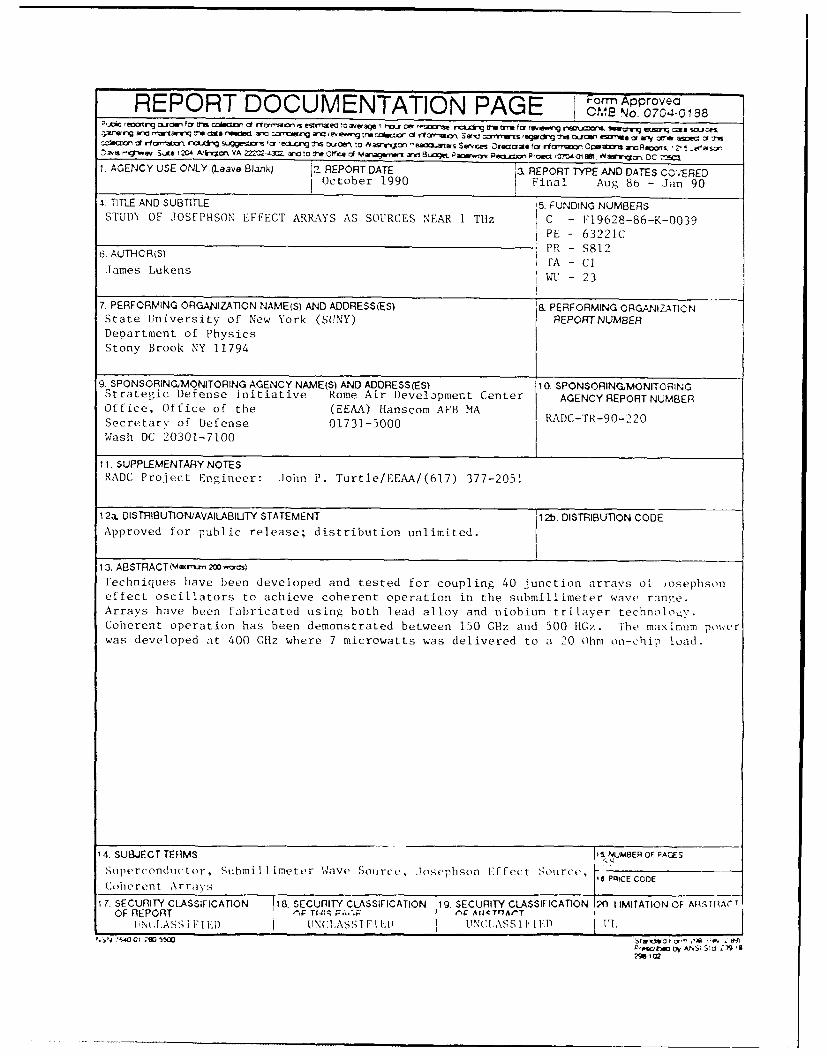
4. TITLE AND SUB 1ITLE 5. FUNDING NUMBERSSTUDY OF JOSEPHSON EFFECT ARRAY S AS SOURCES NEAR 1 THz C - 1:19628-86-K-0039
PE - 63-921C
6. AUTHOR(S)PR-S1FA - Ci
James Lukens W'- 23
7PERFORMING ORGANIZATION NAME(S) AND ADDRESS(ES) & PRPORMIN NUBRANZIOState University of New York (SUNY)REOTNMRDepartment of Physics
Stony Brook NY 11794
9. SPONSORING,?vONITORING AGENCY NAME(S) AND ADDRESS(ES) 10. SPONSORIN(iMONITO:RINGStrategic Defense Initiative Rome Air Development Center AGENCY REPORT NUMBEROffice, Office of the (EEAA) Hanscom AFB MA RADC-TR-90-220Secretary of Defense 01731-5000
Wash DC 20301-71001
i I. SUPPLEMENTARY NOTESRADC Project Engineer: John P. Turtle/EEAA/(617) 377-2051
1 2a. DISTRIBUTION/AVAILABIUTY STATEMENT 1i2b. DISTRIBUTION CODEApproved for public release; distribution unlimited.
13. ABSTRACTi'4-r- 2 -oa,
Techniques have been developed and tested for coupling 40 junction arrays of Josephsoneffect oscillators to achieve coherent operation in the submillimeter wave range.Arrays have been fabricated using both lead alloy and niobium trilayer technoloi'y.
Coherent operation has been demonstrated between 150 GHz and 500 H(;z. The maximum powerwas developed at 400 (;Hz where 7 microwatts was delivered to a 20 Ohm on-chipj- load.
1 4. SUBJECT TERMS I INUMBER OF PAGES
Supe rc onduc t o r, Stihm i I I ime tevr Wave Soui rc e, Josephi son 1E.ffCc t sou rce,~~C
(;ohcren t Arrays
17. SECURITY CL-ASSIFICATION 18a. SECURITY CLASSIFICATION 1i9, SECURITY CLASSIFICATION 20 1 IMITATION OF Ail.;T nAr TOF REPORT I- T":q n C7 AnCTT7Af(TI
Pstma oy ANS; S:o Z39 'B2WI 0
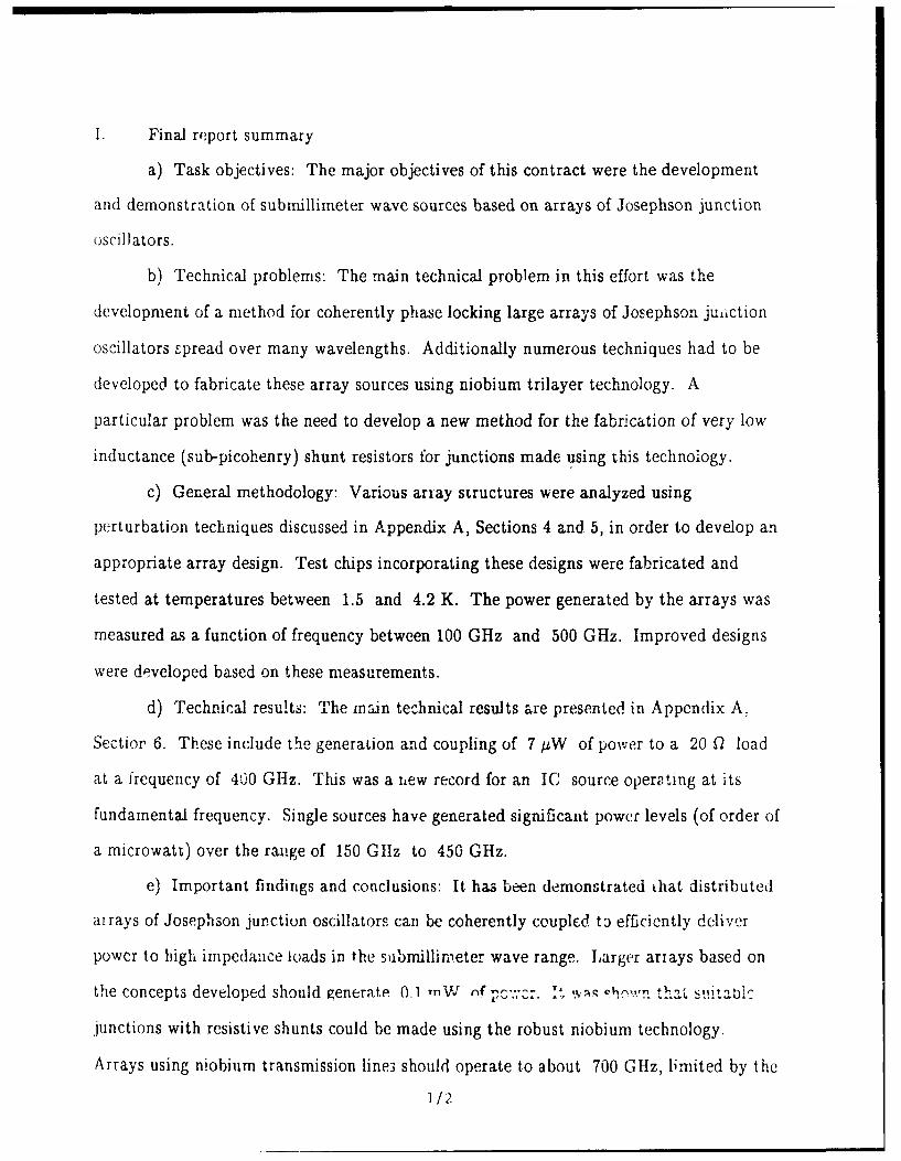
I. Final report summary
a) Task objectives: The major objectives of this contract were the development
and demonstration of submillimeter wave sources based on arrays of Josephson junction
oscillators.
b) Technical problems: The main technical problem in this effort was the
development of a method for coherently phase locking large arrays of Josephson juiction
oscillators spread over many wavelengths. Additionally numerous techniques had to be
developed to fabricate these array sources using niobium trilayer technology. A
particular problem was the need to develop a new method for the fabrication of very low
inductance (sub-picohenry) shunt resistors for junctions made using this technology.
c) General methodology: Various ariay structures were analyzed using
perturbation techniques discussed in Appendix A, Sections 4 and 5, in order to develop an
appropriate array design. Test chips incorporating these designs were fabricated and
tested at temperatures between 1.5 and 4.2 K. The power generated by the arrays was
measured as a function of frequency between 100 GHz and 500 GHz. Improved designs
were developed based on these measurements.
d) Technical resu!ts: The main technical results are presented in Appendix A,
Sectior 6. These include the generation and coupling of 7 AW of power to a 20 02 load
at a frequency of 4!0 GHz. This was a xew record for an IC source operating at its
fundamental frequency. Single sources have generated significant power levels (of order of
a microwatt) over the range of 150 GlIz to 450 GHz.
e) Important findings and conclusions: It has been demonstrated that distributed
ai rays of Josephson junction oscillators can be coherently coupled to efficiently deliver
power to high impedance loads in the submillimeter wave range. Larger arrays based on
the concepts developed should generate 0.1 ,nW nf : " ; P o .n that suita.i..
junctions with resistive shunts could be made using the robust niobium technology.
Arrays using niobium transmission lines should operate to about 700 GHz, limited by the
1/2
losses in the lines. Using a higher T, material, e.g., NbN for the transmission lines but
continuing to use Nb junctions, should increase the upper limit to about 1.5 Tltz.
f) Implications for further research: Our results have suggested methods to
extend both the frequency and power of array sources. These techniques, which are
discussed in more detail in Appendix A, Section 7, include the use of high T, materials
and of arrays using wide junction and/or having a two-dimensional distribution of
junctions in contrast to the one-dimensional arrays studied under the present contract.
g) Significant hardware development: The main hardware developed as part of
this contract was the 40 junction array IC discussed above and in more detail in
Section 6 of Appendix A.
II. Scientists and engineers contributing to report
Dr. Aloke K. Jain
Mr. Joseph Montani
Mr. Yi Liu
Mr. Kelin Wan
Mr. To Chi Leung
Mr. Baokang Bi
Mr. Lan Vu
Mr. Linus Fetter
Professor James Lukens
III. Publications resulting from work supported under this contract
"Josephson Arrays as High Frequency Sources"James LukensChapter in Modern Superconducting Devices, S. Ruggiero and D. Rudman, Eds., AcademicPress, Boston, 1990.
"Submilirieter Wave (leneration Using Josephson Junction Arrays"K. Wan, A.K. Jain, J.E. LukensAppl. Phys. Lett. 63, 1805 - 1807 (1989)
3

"Submillimeter Wave Generation Using Josephson Junction Arrays"K-L. Wan, A.K. Jain, J.E. LukensIEEE Trans. Magn., MAG-25, 1076-1079 (1989)
"Application of Josephson Effect Arrays for Submillimeter Sources"J.E. Lukens, A.K. Jain, and K.L. WanSuperconducting Electronics, H. Weinstock and M. Nisenoff, Eds. NATO ASI Series(Proceedings of the NATO Advanced Study Institute on Superconducting Electronics, heldin I1 Ciocco, Italy, June 26 - July 8, 1988), Series F: Computer and Systems Sciences Vol.59 , Springer-Verlag, 1989.
"Using the Josephson Effect for Millimeter and Submillimeter Wave Ge.eration"J. Sauvageau, A.K. Jain, J.E. LukensSensing, Discrimination, and Signal Processing and Superconducting Materials andInstrumentation, Roy Nichols, James A. Ionson, Eds., Proc. SPIE 879, 69-70 (1988)
"Phase-locking in Distributed Arrays of Josephson Oscillators"J.E. Sauvageau, A.K. Jain, J.E. Lukens, R.H. OnoIEEE Trans. Magn., MAG-23, No. 2, 1048-1050 (1987)
IV. Recapitulation of periodic reports
The major effort during the first period was the acquisition and and initial
construction of equipment needed for this research. We worked to develop a new electron
beam lithography system to permit writing of arrays over large areas of a wafer. Work
also began to test the performance of our Josephson junctions at frequencies up to 1 Tttz.
These areas would be thL focus of work during the coming three month period.
During the second period the scanning electron microscope and other components
arrived for the new EBL (electron beam lithography) system which we would be building
and which would be crucial for the large arrays to be fabricated during the later stages of
this project. Work began to interface the beam control electronics to a comuter for
pattern generation. Work also began on building the laser interferometer controlled stage
for positioning the wafers during beam writing. Measurements were made to test the
performance of our resistively shunted lead alloy junctions at high frequencies. Data
indicated that their performance was essentially ideal up to at least 600 GHz. This was
near the useful upper limit of lead due to excessive transmission line losses at high
frequencies. We thus concluded, as anticipated, that the lead alloy technology would be
-,,,,, ,n,-,- m nimm nm mmmilltinmiN
adequate for the first phase of the project. For operation above one terahertz, refractory
metals, e.g. NbN, would be required. In anticipation of this, work w.- begun to construct
a plasma etching system required for pattcining the Nb films.
In period three the developr.'ent work proceeded as expected. In particular the
beam control hardware for our new, large field EBL system was nearly finished, and work
continued to develop NbALNb trilayers for later use in high frequency circuits. The
results of our AFOSR-sponsored project to test concepts for a 100 GHz Josephson array
source demonstrated that the design for phase-locking the junctions in distributed arrays,
which we planned to use for the THz sources, performed as expected. However, as a
result of that work we concluded that the junction uniformity required for a fully phase-
locked array implied a critical current spread with a standard deviation of less than about
1% -- about half that expected when we began the work. A potential solution to this
problem, which would avoid the necessity to upgrade our present junction fabrication
process, was to current bias the junctions in parallel instead of in series. In this way the
bias currents automatically divide up so as to compensate, to first order, for the
nonuniformity in junction critical currents. One drawback to this approach was that it
was necessary to carefully filter the many bias leads to the array in ordar to avoid
perturbing its rf properties. Our first tests of this new design were encouraging in that
the power increased by a factor of ten over that from a similar series biased ariay, giving
0.04gW at 300 GJIz. This first attempt had rather crude rf filters on the bias leads.
We expected that this poor filtering was the reaon that the theoretical power of 0.1kAW
was not achieved and started work to refine the design of these filters.
Our major result during the fourth period was to obtain power levels of about
IW from Josephson effect arrays operating near 300 Gflz. The "breakthrough" which
led to these results was the parallel biasing scheme previously reported. In that array the
junction spacing was 1mm, the wavelength at 100 GHz. Since this array preferred to
operate at 300 GHz, presumably because of the load impedance seen by the junctions, we
5
reduced the junction spacing by a factor of 3 to give a fundamental operating frequency of
300 GHz. This, along with some refinements in coupling the bias leads to the array,
resulted in a series of three arrays with power levels of 0 2pW, 0.4MW, and 0.8AW. The
IR product of the junctions used in these arrays corresponded to a frequency of 75 GHz,
far below the operating frequency. This was caused by the relatively low critical current2of about 300AA. Since power would increase as Ic under these conditions, the prospect
existed for a substantial power increase just by increasing I.
Our primary effort during the fifth period was to conduct a series of systematic
measurements on the parallel biased arrays from which we had been obtaining lj1W of
power at 350 GHz. For example, we were measuring properties of the individual
junctions comprising the array in order to more accurately compare our results with
theory. In addition, measurements were started to determine the temperature dependent
attenuation of the microstrip transmission line in the array as well as the effects of the
multiple bias lead on the array. This work involved both the fabrication of samples
specially designed to test these various properties as well as the development of computer
software to simulate the predicted response of the circuits. The development of the
computer interfacing and software needed for the conversion of our new SEM into an EBL
system was now essentially complete, and we were now using this system, purchased with
DOD URIP funds, for our mask fabrication.
During the sixth period the effects of a range of array parameters were studied in
order to optimize the array design for higher power and to improve our understanding of
its operation.
1. Parallel bias.d arrays with two independently biasable sections were fabricated
and studied. The array could be operated with either one or both sections biased at the
operating voltage. Measurements were made of load power as a function of which sections
were in operation. it was observed that the load current with both sections operating was
more than the sum of the currents of the two individual sections. This led to the
0

conclusion that the higher transmission line current when both sections were in operation
produced additional phase alignment of the junctions. It was also observed that the two
sections of the array phase-lock to each other. That is, the current through one section
could be varied relative to the other over a certain range but the two sections would
continue to operate at the same frequency. The strength of the phase-locking provided an
independent measure of the amplitude of the load current, which was consistent with that
measured by the detector junction. The overall power of these arrays continued to be in
the 1 - 2 uW range.
2. The shunted junctions in the array had both parasitic capacitance and
inductance. Analytic results for the RSJ model thus did not exactly predict their
performance. This was particularly important in our use of the amplitude of the
Josephson current step to measure rf power. We carried out computer simulations based
on more realistic junction models. We were confident, based on this refined analysis, that
our power estimates were accurate within a factor of two.
3. It was discovered after considerable testing that there was a minimum base
electrode thickness and a minimum critical current for which the arrays would operate.
We did not have enough personnel to investigate this problem in more detail; however, it
did explain why some of our earlier arrays did not work and enabled the fabrication of
arrays which consistently operated with microwatt powers.
The work done on junction development (Pb alloy) during the seventh period was
as follows:
1. Work was carried out to increase the critical current and IcR products of our
resistively shunted junctions. This was needed in order to obtain the higher power and
operating frequencies which were required. To date it had been possible to increase 1c to
2.5mA and the IR product to 1.3mV in shunted junctions without heating or other
problems degrading their performance.
2. The upper operating frequency for the lead alloy junctions was measured by
7
putting two junctions in a small loop in order to measure theii phase locking as a function
of frequency. Note that in the arrays the upper frequency limit is determined by the
losses in the lead alloy transmission lines. This occurs at about half the cutoff frequency
of the junctions. The frequency limit for our junctions, measured in a small loop, was
1 Tiz. This was the expected cutoff based on the measured gap voltage from the I-V
curve. (The copper shunt under the junctions reduces the gap some from the standard
value.)
3. Fabrication teciiiiiques were improved, permitting the fabrication of larger area
junctions. The width of the junctions was successfully increased from lm to 4jtm.
The difficulty in doing this using our self-aligned masking technique was that the mask is
suspended above the substrate for a span equat to the junction' width. These greater
width junctions, however, have several advantages. The greater area improves heat
dissipation, permitting larger values of I. In addition, the reduced critical current
density permits an increase in capacitance and thus in 0c, the damping parameter. This
made it possible to achieve values of 0, needed for optimum locking strength among the
junctions.
Our major result during period eight was the fabrication and testing of improved
array designs making use of the developments in junction technclogy and in our
understanding of array operation resulting from work earlier this year. Such an array
gave a five fold peak power increase (to 7AW) over those tested earlier in the year. Power
levels above l1IW were achieved for a number of frequencies in the range of 340 Gtlz to
110 Gllz; however, tat, array was not continuously tunable throughout the range. A good
understanding of the tuning range for these arrays needed to be developed. Work was
progressing on the implementation of the Nb trilayer process for junction fabrication.
We expected that the next major advance in array power would make use of these
junctions since we were shifting emphasis from further improvements i, lead alloy
junctions to Nb - and probably then to NbN-junctions. At that time very high qualitv
8
Nb junctions with critical current densities up to about 1000A/cm 2 were being
fabricated. We were aiming to get this up to about 104A/cm 2 but, more importantly, to
develop techniques for making the junctions nonhysteretic at the frequencies of interest.
This meant that we could not just import the process (or finished trilayers) from other
labs but must develop processes tailored to our own needs.
The upper frequency limit of our arrays at that time was set not by the junctions
but by the losses in the lead alloy microstrip. We worked with the group at JPL to
make a "hybrid" array having an NbN ground plane and microstrip. In this work we
did the design, mask fabrication an, junction fabrication, with JPL depositing and
patterning the NbN film and dielectric layer. One complete sample was fabricated in
this manner. This served mainly to highlight a number of refinements needed in the
processing.
We have now succeeded in the fabrication and testing of a successful array using
iobium junctions with aluminum oxide barriers. This array, which used the same design
as our previous lead alloy arrays, generated a maximum power of about 1 AW into a
20 0 load. It operated over the same frequency range as the lead arrays and had an
estimated linewidth of about 100KHz. The Nb junctions used had 700 PA critical
currents and were shunted with 0.50 low inductance (: 0.1 pH) resistors. This critical
current was still about a factor of 4 less than the maximum for our lead arrays, which
accounted for the somewhat lower power.
9
Appendix A
1. Introduction.
There is a rapidly developing need for compact submillimeter sources for use in such
applications as satellite communications and receivers for astronomical observation.
Fundamental solid state oscillators such as Gunn or IMPATT diodes are presentl, limited
to the millimeter wave range, leaving such bulky and power hungry sources as carcinotrons
and CO 2 lasers which operate in some parts of the submillimeter range.
Josephson junctions are natural voltage controlled oscillators, and it has been
recognized since the discovery of the Josephson effect that these junctions have the
potential for filling this source gap at least up to frequencies of several terahertz. As the
Josephson equations imply, the average frequency of supercurrent oscillation vo , which we
call the Josephson frequency, in a junction is related to the dc component V of the
voltage across the junction only through fundamental constants,
, h (1.1)
where e is the charge on the electron and h is Planck's constant, so
2e/h = 483Ghz/mV. Indeed this remarkable result has been shown (Tsai et al., 1983 and
Jain et al., 1987) to be independent of the materials or structure of the junction to better
than I part in 10 One would thus hope that Josephson junctions would be useful
tunable sources operating up to the superconducting gap frequency - a few THz for
conventional superconductors and perhaps tens of TIIz for the new high T, materials.
fTnless the junction voltage is constant in time, i e., V(t) = V, Eq. 1.1 does not
necessarily imply a pure sinusoidal oscillation with frequency proportional to the dc
voltage. In practice, at high frequencies, it is usually easier to control the junction's bias
current than its voltage Indeed, there are many examples in the literature, such as chaotic
behavior or periodic mode-locking to resonant structures, where, even though Eq. 1.1 is
satisfied, almost none of the power generated by the junction is at the frequency V0.
Although a great deal of wu'k in many laboratories has gone into the development of
practical sources based on the Josephson effect, the serious problems related to the very
low power and source impedance of individual junctions in addition to that of obtaining
spectrally pure oscillation at the Josephson frequency have been difficult to surmount. One
technique for overcoming these problems, which will be the focus of this chapter, is to use
arrays of junctions in place of single junction sources. The discussion presented here has
evolved from a lecture at the Nato Advanced Study Institute on Superconducting
Electronics (Lukens, et al., 1989).
First, the properties of single junction sources will be revipwed in order to get a
perspective on the problems to be solved. After a brief look at the performance expected
from idealized arrays, perturbative techniques for analyzing arrays will be developed based
on the resistively shunted junction (RSJ) model. While this model is clearly only
approximately correct for real tunnel junctions, it can produce analytic results useful for
achieving an insight into the design of coherent arrays. These results have proven to
provide a very good description of many of the experiments to date. The final parts of this
chapter will present a number of recent results for practical array sources where the
junctions are distributed over many wavelengths as well as speculations on future
directions for research.
2. Single junction sources
2.1 Small junctions
The properties of single junction sources will be described first in order to see where
arrays may be useful. The RSJ model (Fig. la) with C = 0 will be used to describe
the junction's behavior since, for this case, analytic solutions exist which provide a useful
insight. See e.g., Likharev, (1986) Chap. 4. When the bias current lb is increased above
1,:, the junction's phase 0 begins to increase with time, producing an oscillating
supercurrent (since 1s = I sin (0)) and consequently an oscillating voltage. For lb near
I,: the voltage waveform is nearly a spike, having a large harmonic content. As 1c is
.. . ... ..... . .. . ... ........... . . . . . . . . ,m n2 1
increased the higher harmonic content of the waveform decreases, giving a nearly sinusoidal
wave for V > V, = I Rj. The amplitudes of the harmonics are given by
= = 2V (2.1.1)
2
where, = V/Vc and i. lb/Ic and for the RSJ model V = (i - 1) Also,
c = 2 ?rVc/o0. This waveform approaches a nearly pure sinusoid for T; > 1 . Since for
most applications one would like a reasonably sinusoidal source, we will impose the
constraint that > 1 at the desired operating frequency.
Since the junction impedance at the Josephson frequency is Z _ Rj for V > 1 , at
high frequencies the junction can be viewed as an oscillator of amplitude V11 at the
Josephson frequency in series with R as shown in Fig. lb. The power available to a
matched load from a single junction is then-2
P- Ic R,, V> 1 (2.1.2)
There are limits on both Ic and R which limit the maximum power obtainable at a
given frequercy. The discussion so far has assumed that the junction is one dimensional,
that is, the phase difference between the electrodes is independent of the position on the
electrode transverse to the direction of tunneling current flow. This, in general, means that
the dimensions of the junction must be limited to assure a constant current density. Since
the natural scale over which current density varies in the junction is the Josephson2
penetration depth A I/(2egOdJc) (where d is the magnetic thickness of the barrier)
keeping the junction's dimensions of order a will assure the required uniformity. For an
in-line junction with critical current density J, , shown in Fig. 2, over a ground plane, the
current is confined (on the x axis) within about 2A3 of the end of the junction giving a
maximum effective critical current in zero field of Ic , 2AJwJc where w is the width of
12
the junction (Basovaish and Broom, 1975). As long as the current feeding the junction is
uniform across the width of the junction ( y axis), a solution exists in which the current
density within the junction is also constant across its width for arbitrarily wide junctions.
At some point instabilities will develop in this uniform solution and limit the
junction's width in practice. A very conservative estimate for this maximum stable width
2would be 2A . Then, since A x 1/Jc, the maximum critical current for a given material
would be independent of Jc and equal to about 4mA for niobium. At the other extreme,
very wide inline junctions are well known to have flux flow across the junction. One might
expect this sort of instability to develop when the electromagnetic wavelength, Aem, in th.
junction was equal to twice the junction width, that is at the first Fiske mode, since for
this condition there will be where strong coupling between the Josephson and fluxon
oscillations. Indeed it has been observed (Kautz, et al., 1987) that the phase-locking of
junctions in voltage standard arrays to external radiation decreases abruptly for wider
junctions. If the first instability is the first Fiske mode, then the maximum junction width
will be given by
We, = 1 (2.1.3)2v( odC 8 )
where Cs is the specific capacitance. This width is independent of Jc but varies
inversely wih frequency. Thus the maximum critical current for this condition would
depend on the critical current density but would decrease with frequency. For example, a
niobium junction with a critical current density of 105A/cm 2 would have a maximum
stable critical current of I t 7.6mA/v[THz].
Having fixed I, R3 should be adjusted using a shunt resistor depending on the
desired operating frequency and limited, of course, by the material dependent intrinsic
I,:R product of the junction. The condition " > 1 for a sinusoidal waveform limits the
13
maximum resistance for a given Ic and frequency v. On the other hand, if R is reduced
below the value for which V = I, Eq. 2.1.2 indicates that the power will decrease. Thus
one should select the shunt resistance such that R, - v 4o/Ic givng
1PI(v) - S v 4>O Ic (2.1.4)
Figure 3 illustrates the source resistance, critical current and available power as a
function of frequency for single junction sources subject to the width constraints discussed
above. For junctions with w = 2A , one sees that the maximum single junction power is
proportional to frequency with
P (v) ; 1 (v[THzI) pW (2.1.5)
Thus, for example, one might expect a maximum power of about 1sW at 1THz. While
this is sufficient for some applications, it is about the limit with proportionately less power
available at lower frequencies. Also the source impedance for this 1/pW source would be
less than an ohm. This would require a substantial transformer ratio for typical loads and
could be a problem if wide tuning were desired. Junctions with w = Aem/2 have the
potential for delivering above a microwatt at lower frequencies but at the expense of even
lower source impcdam-us.
2.2 Fluxon oscillators (wide junctions).
There are several groups which have reported significant power levels at. frequenc> ,,
up to several hundred gigahertz from fluxon propagation in very wide junctions. While tiL,,
focus of this chapter will be on series arrays of junctions small enough to have a spacially
u Piforrn current density, we will briefly review these results for fluxon oscillators for the
'i te whi 1ev 1 t.roviic,. nm the possible ad \antagc{es and .!il ;dvantagcs of this typk
of source.
Si,:iific;it pov, er 1:, [wl 'n ,bservcd frr twI! differct tNpI's f fiuxon ,m scillatrs
The first, which uses unidirectional flow, has been studied mainly in Japan (Yoshida, et al.,
1989 and Nagatsuma, et al., 1983). In this type of oscillator, a magnetic field is applied in
the plane of the junction, along the x axis (Fig. 2) to form flux vortices or fluxons in the
junction. The bias current then forces the vortices to flow across the junction (along the v
axis) along the transmission line formed by the base and counter electrodes. If the bias
current is increased until the vortices are moving near the speed of light in the junction,
voltage and thus the frequency becomes insensitive to small changes in the bias, i.e., the
junction has very low differential resistance. The frequency can be tuned over a wide range
by varying the vortex density in the junction by changing the applied field. It is estimated
(Nagatsuma et al., 1983) that of the order of a microwatt of power should be available from
such oscillators at frequencies ranging from about 100GHz to- 1 THz and powers of this
magnitude coupled to an SIS detector at the end of the junction transmission line have
been reported up to 400GHz. A problem associated with this type of oscillator is that the
characteristic impedance, which is that of the transmission line formed by the junction, is
in general quite low. Transformers have been developed (Yoshida, et al., 1989) to couple
power more efficiently to higher impedance loads and have succeeded in coupling about
0.1 AgW to a 1 2 load at 200GHz. The penalty for using these resonant transformers,
however, is that the tuning range is severely restricted.
The second type of fluxon oscillator, which has been studied primarily by groups in
Europe, has a similar geometry but uses a high Q resonant junction. These resonant
fluxon oscillators are operated on their zero field steps, the operating frequency being
determined by the dimensions of the junction rather than an applied field. Two groups
have recently reported detecting power levels of the order of 0.1 'UW from such junctions.
One group (Cirillo et al., 1989) reported radiation at 75 GHz using on chip detection with
small junctions. The oscillator junctions had a transmission line impedance of 1 Q and an
estimated available power of about 0.1 jW . Simulations show a steplike structure in
junction's phase vs. time indicating a large harmonic content to the radiation as one might
15

expect from the picture of fluxons shuttling back and forth in the junction. A second group
(Monaco et al., 1988 and Pagano et al., 1989) reported radiation near 10 GHz from an
array of resonant fluxon oscillators in which a significant degree of phase-locking among the
junctions was observed. In this case the radiation was coupled to a detector outside of the
cryostat. Power levels of c-ver 0. 1 jLW in a 50 0 load were reported. In smaller arrays,
where more complete lockng could be achieved, linewidths of several kilohertz were
observed.
2.3 Radiation linewidth
A final consideration related to single junction sources is their linewidth. The
linewidth of the Josephson radiation is determined by frequency modulation due to low
frcquency voltage noise across the junction, (Likharev and Semenov, 1972) with frequencies
up to about the linewidth A' being important. In terms of the current noise in the
junction,
12,) pR (23.1)Au = s~. 5(0) R 231
Here SI(0) is the low frequency current spectral density, and Rd is the differential
resistance at the operating voltage. If S1 (0) is just the Johnson noise current of the
junction resistance R, and Rd - R, then Au z 160 MHz per ohm of junction resistance at
4 K . This is only a rough guide, since S,(O) will in general be increased due to such
things as 1/f noise prevalent in high J, junctions, as well as to down-converted quantum
nOise fromn iwar the ,Jose)hson frequency. On the positive side, !:ince only low frequency
noise is important in determining Au, one can in principle make the linewidth arbitrarily
small by shunting the junction at low frequencies without reducing its high frequency
impedance. This technique has been successfully used (Smith et al., 1987), although it can
have drawbacks such as the introduction of instabilities or chaotic behavior.
Another technique for linewidth reduction is to reduce the differential resistance of

the junction at the operating point through coupling to a resonant structure. An example
of this is the fluxon oscillations in resonant wide junctions discussed above. These
junctions can have very low differential resistance when biased on their zero field steps.
The situation with unidirectional flux-flow is more complex. While the differential
resistance is also small at the operating point, the junctions are tunable by varying the
flux, so the linewidth will to some extent be affected by fluctuations of the flux linking the
junctions, perhaps more than by spacially uniform fluctuations in the bias current.
One can summarize the properties of single junction sources by saying that, in
general, such sources have either too little power, too low an impedance, too broad a
linewidth or all of the above, although the power and impedance begin to become useful for
some applications as terahertz frequencies are approached. Next we will take a brief,
rather elementary look at small junction arrays to see to what extent the replacement of
single junctions by arrays of junctions might solve these problems.
3. Arrays
Interest in Josephson arrays was sparked in the late 1960's by experiments of Clark
(1968) and a paper by Tilley (1970) who predicted superradiance in such arrayc, much as in
a collection of atoms in a cavity. One signature of this superradiance was a prediction that
the output power would scale as the square of the number of junctions. This led to a hope -
rather naive in retrospect - that significant power levels could be obtained from Josephson
junctions simply by connecting a large number of junctions together without worrying in
detail about just how they were coupled. The initial experiments were done by Clark
(1973) and (1968) on two-dimensional arrays of superconducting balls, which were
Josephson-coupled through their oxide coating as shown in Fig. 4b. Indeed, evidence of
interactions among the junctions was seen; however experiments of this type have never
produced significant levels of power. As will be seen later, when the details of how
junctions phase-lock is discussed, for arrays of this type power is mostly dissipated in the
array itself. The development of Josephson-effect arrays, involving hundreds of workers,
17

has been covered in detail in two review papers by Jain et al., (1984) (JLLS) and by
Lindelof and Hansen (1984) and more recently in a book by Likharev, (1986). Readers are
referred to these sources for a comprehensive review.
In more recent work, including successful attempts to obtain increased power from
arrays of junctions, the junctions are simply treated as classical oscillators, i.e., the
junction's current and phase are taken to be classical variables as in the discussion of
single-junction sources above. This is the approach taken throughout this chapter. It is
worth emphasizing the distinction between the present work based on the classical picture
and the initial discussion of Josephson arrays in terms of superradiance, since much
confusion has been caused over the years by not fully appreciating this distinction. This
confusion has been compounded by the fact that there have been observations of the power
from arrays increasing as N2 , as predicted for superradiance. As far as we know, all these
observations can be explained in terms of purely classical circuit analysis, as will be seen,
for example, below.
Probably the simplest example of the advantages to be gained from arrays of
junctions can be seen by considering the one-dimensional array shown in Fig. 4a. Here a
number of junctions are connected, e.g., by a transmission line, in series with each other
and with the load to be driven, RL , so that the rf current generated by a junction flows
through all of the other junctions and the load. Representing each junction by its high
frequency equivalent circuit (Fig. 1b), which to first order is not affected by the rf
current, one sees that the array impedance can be matched to the load by taking the
number of junctions to be N = RL/RJ ,thus solving the low impedance problem of single
junction sources. For now it is simply assumed that all of the junctions will oscillate at the
same frequency and in-phase. The discussion of the conditions needed for such phase-
locking will occupy much of the remaining sections of this chapter. It will also be assumed
for now that the circuit dimensions are small compared to the wavelength in the
transmission line at the frequency of operation so that the lumped circuit approximation
18

can be used. The constraints on Ic and R discussed in Sec. 2 can then be used to
estimate the number of junctions needed to match a 50 n2 load to an array designed to
operate near a frequency v , giving
R ( 100/v[THz], w= 2Aj
N 200/v [THz] , w = A,n/2
Here the two estimates for N correspond to the limits on the width of the small junctions5 2
as discussed in Sec. 2, taking Jc = 105 A/cm
The available power from this one-dimensional array is just N times that available
from z single junction in the array. Which, for the 50 £2 load is
0. 1mW w=2Aj
:X =NP -I RL { 0. 4mW W = Aem/2 (3.2)v[Ttt z I2w
If it is possible to match an array of any size to a load using a transformer, then the
dependence of power on array size is linear in the number of junctions. The enormous
impedance mismatch between a single junction and a typical load makes the use of
transformers problematical, especially if much tuning range is to be preserved. Without
transformers, situations occur where, when the number of junctions is varied, the load2
power varies as N . For example, this happens when the number of junctions is increased
but the total array impedance is small compared to that of the load. An N dependence
also occurs if an array of junctions with Ic < I, max is matched to the load by reducing
R as N increases such that NRj and IcRJ remain constant. Thus, for many practical
situations the power from arrays is expected to increase as N . These situations are
clearly purely classical in nature but are sometimes confused with superradiance.
Next, one could ask whether anything is gained by replacing the one-dimensional
19

array by a two-dimensional array, as in Figs. 4b-d. We imagine making such an array by
replacing each junction in Fig. 4a by a parallel (transverse to the rf current) string of
junctions, M junctions wide as in Fig. 4c. If all of these junctions were identical and all
oscillated in phase, this would be equivalent to replacing each junction in Fig. 4a with a
junction having IC = Mlc and R, = RJ/M. One would then need M times as many of
these series junctions to match the load; thus the power delivered to the load would be
increased by a factor M'.
As an example, at 1 THz approximately 100 junctions with w = 2A would be
required in a one-dimensional array to match a 50 l load, producing in a power of 0.1 mW.
If a two-dimensional array were used with a width M = 100, then the matched array
would have 10' junctions and deliver 1 watt of power. It is not difficult to fabricate a
million-junction array with modern lithographic techniques. The real question is whether
all of the junctions could be made to oscillate in phase as assumed above, particularly since
the motivation for thinking about a two-dimensional array is that the useful critical current
of a single junction is limited due to phase instabilities that arise at larger values of Ic.
Similar power estimates are obtained for the configuration shown in Fig. 4d.
The arrays discussed above (Figs. 4a, c, d) could all be called linear arrays, since for
proper operation the phase should vary only in one direction, even in the two-dimensional
arrays. It is important to distinguish this situation from truly two-dimensional arrays
(Fig. 4b) where the phase varies in both dimensions. There has been a great deal of very
interesting work, primarily to study phase transitions, in these latter arrays. This work
will be completely ignored here, since it really does not address the problems related to
using Josephson arrays as radiation sources.
4. Phase-locking
It should be clear from the brief discussion above that the real key to the usefulness
of arrays is how, or if, the junctions phase-lock. Even if all of the junctions are identical,
one must still ask if the "uniform phase" condition (in which all junctions have the same
20
phase relative to the locking current) is a solution, and if so is it a stable solution. If there
is such a stable solution, the next problem is to find out what happens if all of the
junctions are not identical. In real arrays there is always some degree of scatter in the
junction parameters, e.g., the critical current, as well as random noise, which tend to make
the junctions of the array oscillate at different frequencies.
It is possib!e to get much insight into both the stability and strength of phase-
locking in arrays by considering the well known phenomenon of a single junction phase-
locking to external radiation. We will start by using perturbation theory to study the
effects of external radiation on an RSJ for which analytic solutions are available. Later,
the effects of junction's capacitance in the low ic (Pc - wcRi C < 1) limit will be included.
The perturbation techniques used are standard and have been applied to Josephson
junctions by several authors (Forder, 1977 and Kuzmin et al., 1981). Here the key ideas of
the theory will be reviewed briefly and then applied to the phase-locking problem. To
begin, a quantity related to the junction phase 0, called the "linearized phase", is defined
by
a= t, (4.1)
where &j is the junction's frequency averaged over a time long compared to a period of a
Josephson oscillation, yet short enough to respond to the low frequency noise and
modulation. The ' symbol is used in general to indicate averaging over the time scale
which is long compared to 1/x. The success of the perturbation theory depends on the
wide separation of the Josephsoii frequency from the low frequency currents which are
important in fixing the linewidth and oscillation frequency.
The essentiat results of the perturbation theory are shown schematically in Fig. 5
where the junction is represented by an equivalent circuit with two parts, one for the high
frequency (HF) (near w) behavior, and the second modeling the low frequency (LF)
response. The high frequency circuit consists of the Josephson oscillator (with amplitude
V1 given by Eq. 2.1.1 and frequency w ) and the source impedance R . This tHF section is
21

coupled to thc LF section through w, which is determined by the LF voltage through the
Josephson equation (Eq. 1.1).
The perturbations which we wish to consider are caused by an rf current IT with a
frequency near w flowing through t- HF terminals. This in turn affects the LF voltage
(and thus w) through the presence of a "mixing current,"
I,= a(2iT cos 0) , (4.2)
in parallel with the bias and noise currents on the LF side. Here a is the conversion
coefficient, which is given in the RSJ model as
1 (4.3)
2(1 + V2)i
The cause of this perturbation might, for example, be either an external rf current source
or a load placed across the HF terminals, or both. So
W =Lu(i + I'),
(4.4)
where the subscript u refers to the value of the variable (w) in the absence of the HF
perturbation. In other words, in the presence of a HF perturbation the junction will
oscillate at the same frequency as an unperturbed junction biased with a current equal to
the sum of the bias and mixing currents in the perturbed junction.
fn order to apply this technique to understand the phase-locking of a junction to
external radiation, we take the perturbing rf current to be that due to an external
current source with amplitude 1e and frequency we near w, so
IT = I, cos (wet) (4.5)
This gives a mixing current
2?
IM Ie cos (be) (4.6)
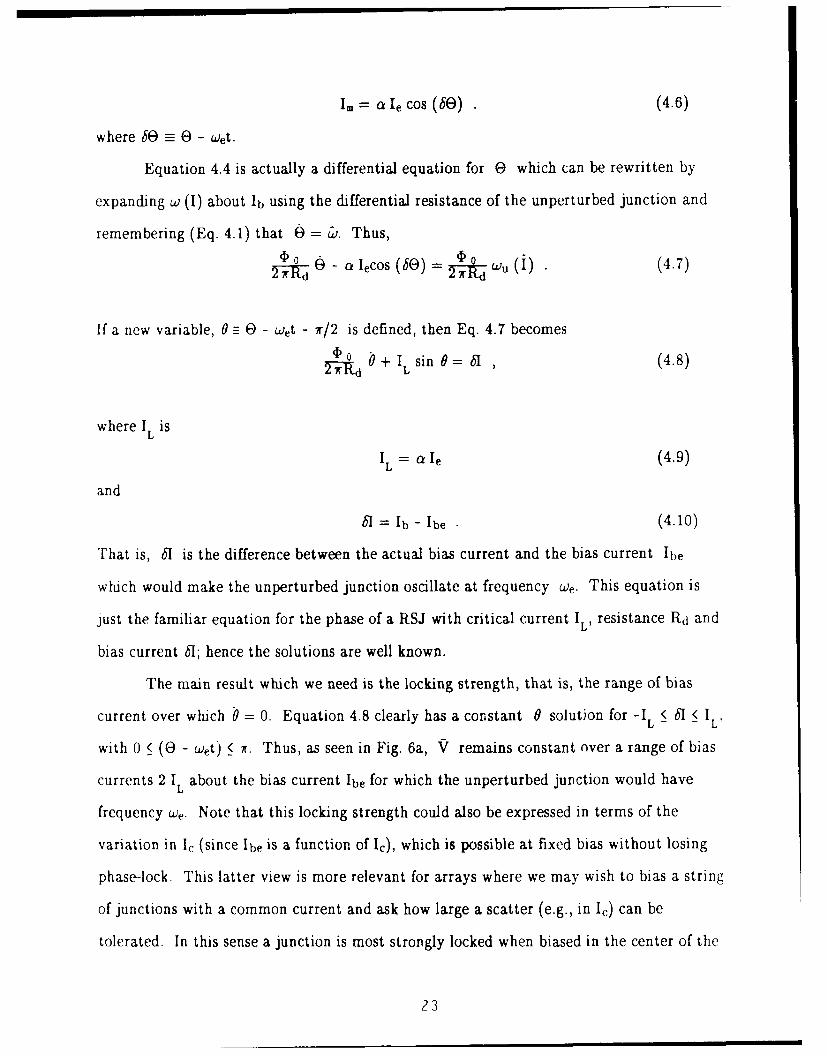
where 66 - 0 - Wet.
Equation 4.4 is actually a differential equation for 9 which can be rewritten by
expanding w (I) about Ib using the differential resistance of the unperturbed junction and
remembering (Eq. 4.1) that 6 = &. Thus,40 - aICs(e (4.7)
If a new variable, 0 = 0 - Wet - ir/2 is defined, then Eq. 4.7 becomes
10 +I sin 0= 61 (4.8)2w-Rd L
where IL is
IL = ale (4.9)
and
61 = Ib - Ibe (4.10)
That is, &I is the difference between the actual bias current and the bias current 1be
which would make the unperturbed junction oscillate at frequency We. This equation is
just the familiar equation for the phase of a RSJ with critical current IL resistance Rd and
bias current 61; hence the solutions are well known.
The main result which we need is the locking strength, that is, the range of bias
current over which 0 = 0. Equation 4.8 clearly has a constant 0 solution for -1L < bI < I
with 0 < (9 - Wet) S 7. Thus, as seen in Fig. 6a, V remains constant over a range of bias
currents 2 1L about the bias current lbe for which the unperturbed junction would have
frequency We. Note that this locking strength could also be expressed in terms of the
variation in I, (since lbe is a function of Ic), which is possible at fixed bias without losing
phase-lock. This latter view is more relevant for arrays where we may wish to bias a string
of junctions with a common current and ask how large a scatter (e.g., in I) can be
tolerated. In this sense a junction is most strongly locked when biased in the center of the
23

current step where the difference between the phase of the junction's oscillation and that of
the external radiation is r/2, i.e., 69 = 4/2. For this bias, the greatest deviation of Ic is
possible in an arbitrary direction. The condition that the phase shift be 7r/2 for strongest
locking has important implications for the design of arrays, as we shall see below. Another
measure of locking strength is the variation in 69 with 51. This is shown in Fig. 6b.
Again one sees that 69 is most stable with respect to changes in 6I for b@ = r/2 and
becomes completely unstable at the edges of the step, bG = 0 or 7r. Note that for the
range of negative 60, where the current leads the oscillator phase, dtO/dbe>0; hence the
phase-locked solution is unstable.
5. Phase-locking in arrays
5.1 Locking strength within the RSJ model.
A detailed analysis of phase-locking in arrays has been carried out in JLLS
(Chap.6), as well as in Likharev, (1986) (Chap. 13). The discussion presented here in
terms of phase-locking to external radiation will, it is hoped, be intuitive while minimizing
the mathematical complications. For large arrays this approach gives nearly the same
results as does the more exact analysis. To begin, consider a series array of identical
junctions, modeled by their HF equivalent circuits and connected in a loop through a load
Zt as shown in Fig. 7. If all of the oscillators have the same phase, then the rf current
which flows in series through all of the junctions and the load is
, (5.1.1)
where the coupling impedance per junction, zc, is given in terms of the load impedance ZI
and the junction impedance RJ as
1= N' (NR,{+Zl) (5.1.2)J
To calculate how much the critical current of one of the junctions can be varied without
having it come unlocked from the array, we can just treat this current as external radiation
assuming that the array is large enough that a variation of the phase of a single junction
24
will have a negligible effect on Il .
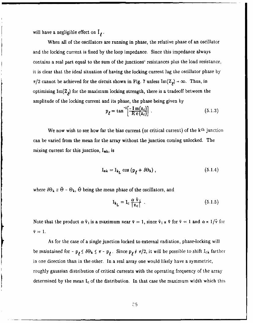
When all of the oscillators are running in phase, the relative phase of an oscillator
and the locking current is fixed by the loop impedance. Since this impedance always
contains a real part equal to the sum of the junctions' resistances plus the load resistance,
it is clear that the ideal situation of having the locking current lag the oscillator phase by
7r/2 cannot be achieved for the circuit shown in Fig. 7 unless Im(Z1 ) -. oo. Thus, in
optimizing Im(ZI) for the maximum locking strength, there is a tradeoff between the
amplitude of the locking current and its phase, the phase being given by
Pt = t an't P e - In mZ (5.1.3)
We now wish to see how far the bias current (or critical current) of the kth junction
can be varied from the mean for the array without the junction coming unlocked. The
mixing current for this junction, Ink, is
Imk = IkL cos (p1 + b0 k) , (5.1.4)
where bek E 19 - Ok, 0 being the mean phase of the oscillators, and
Ik= Ic . (5.1.5)
Note that the product a v is a maximum near i = 1, since vl ax V for V << 1 and a r 1/v, for
>> 1.
As for the case of a single junction locked to external radiation, phase-locking will
be maintained for - pt - 66 k ir - p,. Since p1 t r/2, it will be possible to shift Ick farther
in one direction than in the other. In a real array one would likely have a symmetric,
roughly gaussian distribution of critical currents with the operating frequency of the array
determined by the mean I of the distribution. In that case the maximum width which this
25
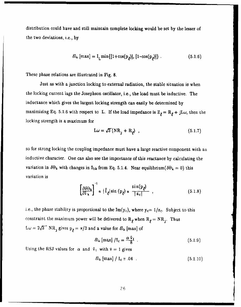
distribution could have and still maintain complete locking would be set by the lesser of
the two deviations, i.e., by
61k [max] = ILmin{[1+cos(pt)], [1-cos(p)]} . (5.1.6)
These phase relations are illustrated in Fig. 8.
Just as with a junction locking to external radiation, the stable situation is when
the locking current lags the Josephson oscillator, i.e., the load must be inductive. The
inductance which gives the largest locking strength can easily be determined by
maximizing Eq. 5.1.6 with respect to L. If the load impedance is Z= = R, + jLw, then the
locking strength is a maximum for
Lw = -'(NR + R) (5.1.7)
so for strong locking the coupling impedance must have a large reactive component with an
inductive character. One can also see the importance of this reactance by calculating the
variation in bOk with changes in Ibk from Eq. 5.1.4. Near equilibrium(60k = 0) this
variation is
[rE01] sin(pI)[&5 kJ t, tllsin (pI), lzclI (5.1.8)
i.e., the phase stability is proportional to the Im(y,), where yc= 1/z,. Subject to this
constraint the maximum power will be delivered to R, when Rt = NRj. Thus
Lw = 2- NRJ gives p, = r/3 and a value for ak [max] of
61 k [max] /I = -2 (5.1.9)
Using the RSJ values for ci and , with V = 1 gives
bIk [max] /I, L .04 . (5.1.10)
26

Therefore, the total spread in Ibk for this type of array can be about 8% before junctions
will start to unlock. Since Ib / Ic is about 1.4 (in the RSJ model) for V = 1, this implies
a permissible variation in Ic of about 10%. This number is a maximum since the spread of
I, for the junctions near the center of the distribution will produce some scatter in their
phases with a consequent small reduction in the locking current I l .
If we are concerned about the unlocking of the first few junctions in the tails of a
large distribution, the estimate above is rather close, as can be shown from computer
simulations (Sauvageau, 1987). It is worth noting that the interaction range of the
junctions in this type of array is essentially infinite, i.e., the interaction of the kth and Ith
junctions does not depend on their separation. As a consequence, the unlocking of several
junctions in a large array has a negligible effect on the phase locking among the remaining
junctions. It ray be undesirable to have even one junction unlocked, however, since if its
frequency is close enough to that of the array, mixing will occur which will modulate the
array frequency to some degree. As the width a of the I distribution is increased and
additional junctions unlock, Il will begin to decrease, causing yet more junctions to unlock
and leading to a rapid uncoupling of the array with increasing a. Computer simulations
on a 40-junction array show that this "catastrophic" failure occurs for a value of a about
twice that at which the junctions in the tail of the distribution first unlock.
We conclude this section with some brief comments on the prospects for 2D linear
arrays. As discussed above, when RSJ's are connected in an inductive loop, their rf
voltage tends to add in-phase around the loop. For the 2D arrays shown in Figs. 4b, c, the
lowest impedance path seen by a junction is the inductive path through the junction in
parallel with it. For these configurations the tendency is for the rf polarities to change
along a parallel chain of junctions with the result that circulating currents are set up
within the chain. Hence power is dissipated internally instead of being coupled to the load.
For the 2D array in Fig. 4d, on the other hand, the lowest impedance path for all of the
series chains is the (presumably inductive) path through the load. Consequently, one
27
would expect a constant phase transverse to the current flow, as desired, for this array.
Capacitive coupling between the chains might further stabilize this situation. These
stability arguments are developed in much greater detaii in JLLS.
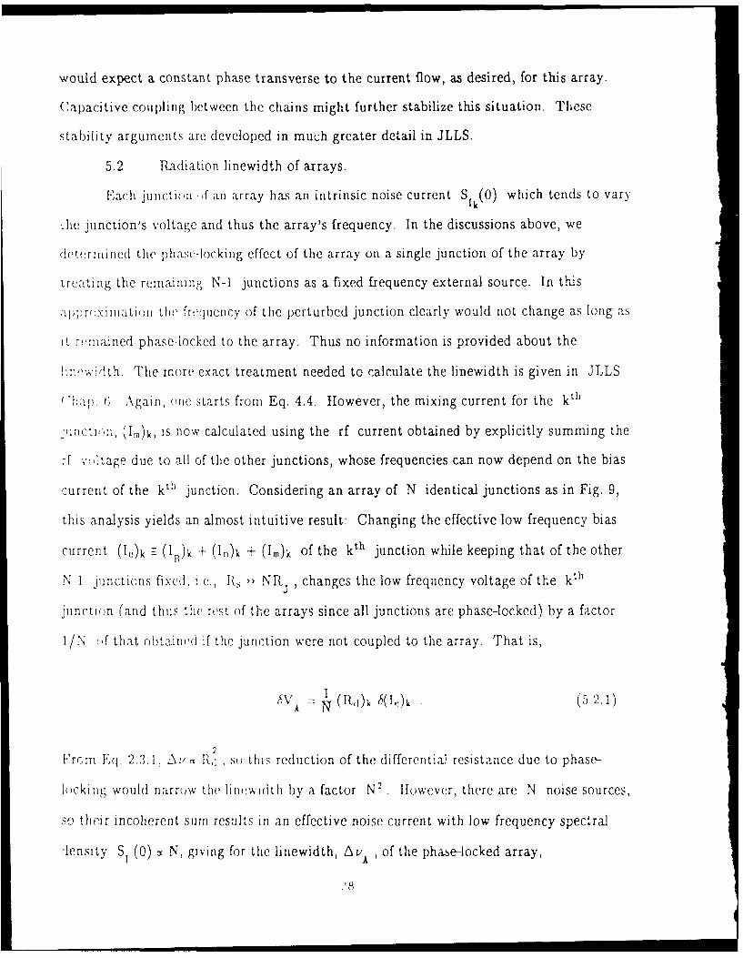
5.2 R1adiation linewidth of arrays.
FEach ju iicti( in if an array has an intrinsic noise current SIk(0) which tends to vary
the junction's voltage and thus the array's frequency. In the discussions above, we
deteruii ned the phase-locking effect of the array on a single junction of the array by
treating the remaining N-1 junctions as a fixed frequency external source. In this
;,. pr,):matiii the frequency of the perturbed junction clearly would not change as long as
t rmained phase-locked to the array. Thus no information is provided about the
,I1.'.Wiith. The more exact treatment needed to calculate the linewidth is given in JLLS
ip G. Again, lie starts from Eq. 4.4. However, the mixing current for the kt h1
n c o,,, (I)k, is now calculated using the rf current obtained by explicitly summing the
.f vltage due to all of the other junctions, whose frequencies can now depend on the bias
current of the kt h junction. Considering an array of N identical junctions as in Fig. 9,
this analysis yields an almost intuitive result: Changing the effective low frequency bias
current (Ie)k = (I,)k + (In)k + (Im)k of the kt h1 junction while keeping that of the other
N-1 junctions fixedI, i.e., I., - NRj , changes the low frequency voltage of the kth
junction (and thus the rest of the arrays since all junctions are phase-locked) by a factor
1/N (,f that obtain i :f the junction were not coupled to the array. That is,
VA == (Ril)k 5(l,.)k .(5.2.1)
2
Frcm Eq. 2.3.1, Ail ,Q so. this reduction of the differential resistance due to phase-
locking would narrow the linwdth by a factor N 2 However, there are N noise sources,
so their incoherent sum results in an effective noise current with low frequency spectral
density S1 (0) o N, giving for the linewidth, AWA, , of the phase-locked array,
.8
A/A -- AvJ (5.2.2)
where AvJ is the linewidth of a junction when it is not coupled to the array. For
example, while a single 0.1 f0 junction would ideally have a linewidth of about 16 MHz,
an array of say 1000 such junctions should have a 16 KHz linewidth. If the junctions'
resistance is varied along with N so that the total array impedance NR, remains
constant, the linewidth would vary as 1/N 2 , e.g., a single 100 fl junction should have a
linewidth of 16 GHz ! As we shall see next, even greater reductions in linewidth are
possible if the effects of low frequency shunting are taken into account.
Consider the case where the low frequency shunt Rs < NRd. Then one can see
from Fig. 9 that the noise voltage generated by the junctions' noise currents is largely
shorted by Rs giving an intrinsic linewidth AVi of
AVt-1 V (5.2.3)/viN / ied ) )
If one takes R, ! Rd this implies a dramatic linewidth reduction in large arrays - by a
factor of N 3 ! This soon reaches the point where the intrinsic noise will be dominated by
coherent noise sources, e.g., by the Johnson noise voltage generated by Rs. Since this2
voltage is divided equally across all the junctions in a phase-locked array, Sv(0) M 1/N
giving a factor N2 reduction in linewidth AVAs due to the shunt. So,
1 1 27 2
AAs 1 -Avs, AVs - (o) kBRsTs (5.2.4)
where T, is the temperature of the shunt and Av, is the linewidth a single junction
would have if its voltage noise were that produced by Rs . This is worth noting since it
implies that, in large arrays, there may not be a penalty in linewidth for using noisy, e.g.,
29
high J, ,junctions.
A possibly scv!re penalty for tlie use of low impedance shunts is the large increase il
bias and cooling power which they can require. Since, roughly speaking, only noise up to
frequencies iv contributes to Av , a shunt in a large array must only be effective at very
N)", fr(qullic( .5 A fatli(t largc i1(luct;lcue should thus be toleralble il serics with the shiuiit
resistor, making it possible to place this resistor, for example, at 77 K . While this would
increase the linewidth due to the shunt, this linewidth would still be so small as to be
acceptable for most applications.
Experimental evidence for the predicted dependence of power and linewith on array
size is shown in Fig. 10 taken from the result of JLLS. Here arrays of 0.1 Q microbridge
junctions incorporated in a 50 Q inicrostrip were measured. The power is seen to increase2
as N as is expected for the coherent state of this array, since the array impedance is
always much less than that of the load (see Sec. 2). Since the low frequency shunting in
this array is negligible, the linewidth is expected to vary as 1/N as observed.
5.3 Effects of capacitance on phase-locking in arrays.
So far only junctions with no capacitance have been considered. In this section we
will examine what changes in the behavior of arrays one might expect if cI#0. One must to
be aware that capalitance is dangerous. A clue to this is seer. in the locking of a single
junction to external radiation where the situation corresponding to a capacitive load, i.e.,
the current phase Icading the oscillator, is unstable. It has been shown that for an array
like that in Fig. 7, the uniform phase solution is unstable if Ze is capacitive (Jain et al.,
1984 and Likharcv, 1986). Instead, the rf voltage tends to sum to zero around the loop.
Further, there are many examples of chaotic behavior in capacitive junctions subject to
applied radiation or external loads. In spite of this there are several reasons to consider
using capacitive junctions in arrays.
Potential advantages of capacitive junctions are: By far the most advanced
technology for making ,Josephson junctions is for tunnel junctions where capacitance is
-- .. , .,,,,n,,,.,, , - -m unnnmu m u i nII
unavoidable. Also, as we shall see below, the presence of a small shunt capacitance can,
under certain conditions, enhance the locking strength in the array. Indeed, there have
been very successful examples of locking large arrays of high capacitance tunnel junctions
to external radiation, (Kautz et al., 1987) as well as demonstrations that even junctions
with fl>l can phase lock and generate radiation (Finnegan and Wahlsten, 1972, Lee and
Schwarz, 1984, Lee and Schwarz, 1986, Kuzmin et al., 1987, Krech and Reidel, 1987, and
Smith et al., 1987). Furthermore, it has been shown that tunnel junctions generate
significant power levels, at least up to the sum of the gap frequencies (Robertazzi et al.,
1988). Fortunately, a very general technique for analyzing the stability of the uniform
solution in arrays with arbitrary fc and Z has been developed by Hadley, Beasley and
Wiesenfeld (HBW) (Hadley et al., 1988 a, b). This should be of great help in desit ling
arrays of capacitive junctions to avoid the "dangerous" regions of parameter space.
In this section the analysis above for arrays of junctions with C = 0 will be
extended, using perturbation theory, to the case of small C, i.e., for tic1, in order to
develop some insight into the effects of capacitance. This low C region near 01, where
one can still hope to obtain meaningful results from perturbation theory, is also the region
in which the analysis of HBW indicates that the uniform solution should have the greatest
stability.
In order to include the effects of junction capacitance, a capacitor will be connected
across the HF terminals of the junction and treated as an additional perturbation. The
details of this analysis, which is summarized below, are shown in more detail in Lukens, et
al., (1989). The effects of the various perturbations to the junction are additive, since the
circuits are linear. The direct effect of the shunt capacitor on the junction will be to
change the voltage IV obtained for a given bias current. This will be ignored since to first
order it does not influence the locking behavior of the junction, but just means that a
slightly different bias must be used to achieve the desired frequency. The most important
effects of the capacitance are to change the effective impedance and rf voltage of the
31
junction as seen by the rest of the circuit. This is illustrated in Fig. 11.
These junctions are now connected in a loop in series with a resistive load having a
resistance, in units of NRj , or r . Tlie phase shift between the junctions' oscillators and
the loop current It produced by the shunt capacitance is p, = tan [ - crt/(rt + 1)],
which has the same sign as that due to an inductance in series with the load. Thus the
phase relationship between the loop current and the oscillators is that required for stable
locking, even with a purely resistive load. The fraction of I which flows throagh R,
ItB , is responsible for the phase-locking. I ti is further shifted with respect to It by a-1(
phase tan ( cV) giving a total phase shift Pt1L between the oscillators and ItI - which
can exceed 7r/2. These phase relations are illustrated in Fig. 12 and show a potential
advantage of the shunt capacitance over a series inductance. Recall from section 5.1 that
the locking strength and hence the acceptable scatter in I, was substantially reduced,
since it was not possible to have a 7r/2 phase shift between the mean phase of oscillators
and the locking current. With a shunt capacitance one can achieve this optimum phase
shift by choosing 3iV- = [--rJThere is a large parameter space in v, i3c and Z that can be explored to optimize
the power and locking strength for a given application. To get a feel for the performance of
these arrays with 0, > 0, let us take the purely resistive load which maximizes the load
power for given ti, and V. This gives
r, = [ I + 2
The desired r/2 phase shift is then obtained for fl, = "--3-. For these values the
locking strength is
I / Ic = a (5.3.2)2F3
32

This is more than twice that for the RSJ array from Eq. 5.1.9, indicating that complete
locking should still be possible with a total spread in I. of greater than 20%. For smaller
values of V the limits of perturbation theory are being pushed, so the exact values need to
be compared with computer simulations. We note that the estimate from perturbation
theory is in line with the result of simulations done by ItBW on 100-junction arrays with
Oc - 0 '5 and i _ 2.3, where locking was still observed with a scatter greater than 15% in
Rj, C and I.
6. Distributed arrays
In all of tte discussions above, it has been assumed that the dimensions of the
arrays were much less than the wavelength A. As a result, the lumped circuit
approximation could be used. To see if this is realistic, note that if the entire array is to
have a length less than A/8 the junction spacings must be
s = !-- 0.1 pxn ,
(6.1)
8
where vp _ 10 m/s is the propagation velocity in the superconducting transmission line
connecting the junctions, and the value of vN from Eq. 3.1 has been used. Unfortunately,
0.1 micron spacing is about two orders of magnitude closer than is practical to place the
junctions in the array when such things as heating and the limits of lithography are
considered. We conclude that in order to achieve maximum power, even from one-
dimensional arrays, the junctions must be distributed over a wavelength or more.
The analysis of phase-locking above has shown that the phase of the junction's
oscillations relative to the locking current flowing in the coupling circuit is crucial. In
general, an oscillator in a transmission line will generate waves propagating in both
directions. This makes it impossible to maintain the same phase relationship between all
of the oscillators and the locking current when the junctions are placed at arbitrary
33
positions along the transmission line. There have been several proposals (Jain et al., 1984,
Davidson, 1981, and Sauvageau et al., 1987 a) for placing junctions along a transmission
line such that they will phase-lock. The simplest approach, described in this section, is just
to place the junctions at wavelength intervals along the transmission line. Hence, all
junctions see the same impedance and the same relative phase. The analysis of this circuit
at the frequency v), , where the spacing is equal to A, is identical to the lumped circuit
analysis above. The disadvantage of this approach is that it is only valid at a discrete set
of frequencies. It is therefore not clear that such an array will be continuously tunable over
a large range of frequencies.
Figure 13 shows a schematic of such a distributed array. The junctions (indicated
by x ) are placed at A intervals along a serpentine microstrip transmission line. An
independently biased detector junction is placed immediately after a load resistor in the
line. By measuring the range of detector bias current over which the detector phase locks
to the array-generated locking current flowing through the load resistor, the power to the
load can be determined for each operating frequency of the array. The ends of the array
are terminated with A/4 stubs so that, to the junctions, the array appears grounded
through the load resistor. Additional length can be added to the stub in order to add a
reactive component to the load to optimize the locking strength.
The current amplitude of the Josephson step in the detector junction of such an
array is shown in Fig. 14 as a function of the average frequency of the array junctions as
determined by measuring the dc voltage across the array (Sauvageau et al., 1987 b). This
array contained 40 junctions, which were biased in series, with the bias current flowing
through the microstrip. The junctions were separated by 1 mm of microstrip giving an
expected value for vx of 100 GHz. Indeed a sharp peak in rf current It through the
detector is observed at 108 GHz indicating the presence of phase-locking near this
frequency. The peak value of the rf current, however, is that expected if only seven of the
forty junctions were locked in-phase. It is possible to directly measure the distribution of
34

critical currents of the junctions in the array; the resulting distribution is in fact too broad
for complete locking. From the measured maximum rf current and the distribution of
Ia's, one concludes that only seven or eight of the junctions could be phase-locked. Thus
the data show that the junctions which are sufficiently uniform to lock, lock with very
nearly the same phase, as predicted.
Since our fabrication process does not yield sufficiently uniform critical currents to
insure that locking would be achieved if all junctions were biased with the same current, a
"parallel" bias scheme has been used. The superconducting bias leads inject (remove)
current at alternate bends in the microstrip, as seen in Fig. 15, with the result that each
junction is part of two interlocking dc SQUIDs. All junctions then have the same average
voltage, which alternates in polarity along the microstrip. This forces the bias current to
divide so as to compensate to first order for the variations in the junctions' critical
currents. The rf locking current is still crucial however, since without it the phase of each
junction would be essentially random due to random flux linking the SQUIDs. Further,
noise currents would cause voltage (and frequency) fluctuations among the junctions.
Phase-locking for this type of parallel biasing has been analyzed in detail in JLLS. It is
primarily as discussed above for series-biased junctions except that the effective scatter in
I, approximately equals 0o/L, where [ is the inductance of the dc SQUID. For this
circuit bl, n! 5 AA. The junctions are resistively shunted lead-alloy tunnel junctions having
an area of about 1.5 pm 2. These resistively shunted junctions, which have Ic = 2.5mA,
have been described in detail elsewhere (Sauvageau et al., 1987 a).
The junctions' separation in this array is 350 pan giving a value for v), of 350 GHz.
The power (as determined from the rf current through the detector and the 23 0 load
resistor) vs. frequency is shown in Fig. 16. Significant power is observed starting at about
ux , however the array also generates over 1 jW of power at a number of discrete
frequencies over a band from 340 GHz to 440 Gllz , where the junctions are not
separated by integer wavelengths. The maximum power of 7 jW is consistent with all 40
3
junctions of the array locked in-phase. Other arrays with lower critical current junctions
are continuously tunable through this band delivering more than 1 £uW of power (Wan, et
al., 1989 a,b), again consistent with all junctions in-phase.
7. Prospects for the future.
As of this writing, the distributed arrays described above are the most powerful
fundamental solid state sources at 400 GHz. Rather straightforward, though technically
complex, extensions of that work should result in sources operating at over 1 THz with
nearly 1 mW of power. Clearly, much work - both experimental and theoretical - needs
to be done. This is especially true when considering wide (w t, Aem/2) junctions and two-
dimensional arrays, where there are essentially no experimental results at present.
Probably the most immediate problem is to couple the submillimeter radiation off chip to
determine its spectral purity. Fortunately, very broadband antennas have recently been
demonstrated in this frequency range (Biuttgenbach et al., 1988 and Li et al., 1988) for use
with superconducting SIS mixers. Also, more theoretical work is needed to understand
the unexpectedly wide tuning range seen in many of the distributed arrays.
Table I summarizes the range of powers and linewidths which might be expected
from several different types of arrays, based on the discussions in this chapter. These range
from one-dimensional, unshunted arrays of narrow junctions in the upper left of the table,
to two-dimensional, linear arrays of the type shown in Fig. 4c, with low frequency shunts,
at the lower right. Essentially the projections in the upper left are rather straightforward
extrapolations of present design, while, moving to the lower right, one ventures into a
territory with progressively more ideas which have yet to be tested. It would, for example,
be surprising if a 1 Hz linewidth at one terahertz were ever achieved.
Finally, it is worth considering what impact the new copper oxide superconductors
(ITS) might have on the development of these array sources. The most straightforward
application of these materials could b as superconducting ground planes and transmission
lines. For a given type of conventional superconductor, e.g., niobium, transmission lines
36

become very lossy at half of the upper frequency limit for the junctions' oscillation. Thus
the upper frequency 'imit might be doubled using HTS microstrip, e.g., to about 3 THz
using NbN junctions. While making high quality tunnel junctions of HTS material may
be some time in the futur, it Is worth remembering that the array oscillators do not
require good tun-(!Iag characteristics. Junctions, e.g., microbridges, with a normal metal
barrier should work well; preliminary reports of such thin film junctions which show the
Josephson effect have already been presented (Schwartz et al., 1939). While the use of
irTS junctiono r-ay well extend the upper frequency limit of Josephson effect sources to
above 10 Tttz, thLc most important advantage ip: 6ially should be to permit opera t ion at
77 K and thus enhance compatibility with many semiconductor systems. From all of this,
we see that Josephson sources h-ve a great, perhaps unique, potential for filling a real void
throughout the submillimeter wave band.
8. Acknowledgements.
I would like to acknowledge the essential contributions of all those at Stony Brook
who have worked so hard over the year on the development of array sources and especially
to thank A.K. Jain, K.-L. Wan and J.E. Sauvagcau, whose work on distributed arrays
pushed Josephson so)urces into the realm of respectability. Special thanks is also due K.K.
Likharev for his valuable and stimulating contributions to our understanding of arrays
made during h,'s summer at Stony Brook. Various aspects of the work on arrays at Stony
Brook have been supported at diffeient times by the Office of Naval Research, the Air
Force Office of Scientific Research and the Strategic Defense Initiative through the Air
Force terahertz t,hnology program.
References
Basovaish, S. and Broom, R.F. (1975). Characteristics of in-line Josephson tunnelinggates. IEEE Trans. Magn., MAG-11, 759-762.
liittenbach, T.t., Miller, R.E., Wengler, MI.J., Watson, D.M., and Phillips, T.G. (198S).A broad-band low-noise SIS receiver for submillimeter astronomy. IEEETrans. Microwave Theory Tech. 36, 1720-1726.
Ciriflo, M., Modena, I., Caretli, P., and Foglietti, V. (1989). Millimeter wave generationby fluxon oscillations in a Josephson junction. J. Appl. Phys., in press.
Clark, T.D. (1968). Experiments on coupled Josephson junctions. Phys. Lett. A 27,585-586.
Clark, T.D. (1973). Electromagnetic properties of point-contact Josephson junctionarrays. Phys. Rev. B 8, 137-162.
Davidson, A. (1981). Now wave phenomena in series Josephson junctions. IEEE TransMagn., MAG-17, 103-106.
Finnegan, T.F. and Wahlsten, S. (1972). Observation of coherent microwave radiationemitted by coupled Josephson junctions. Appl. Phys. Lett. 21, 541-544.
Forder, P.W. (1977). A useful simplification of the resistively shunted junction model ofa Josephson weak-link. J. Phys. D 10, 1413-1436.
Hladley, P., Beasley, M.R., and Wiesenfeld, K. (1988 a). Phase-locking of Josephsonjunction arays. App!. Phys. Lett. 52, 1619-1621.
fladlew, P., Beasley, M.R., and Wiesenfeld, K. (1988 b). Phase-locking of Josephsonjunction series arrays. Phys. Rev. B 38, 8712-8719.
Jain, A.K., Likharev, K.K., Lukens, J.E., and Sauvageau, J.E. (1984). Mutual phase-locking in Josephson junction arrays. Phys. Rep. 109, 309-426.
Jain, A.K., Lukens, J.E., and Tsai, J.-S. (1987). Test for relativistic gravitational effectson charged particles. Phys. Rev. Lett. 58, 1165-1168.
Kautz, R.L., Hamilton, C.A., and Lloyd, Frances L. (1987). Series-array Josephsonvoltage standards. IEEE Trans. Magn., MAG-23, 883-890.
Krech, V.W. and M. Reidel (1987). Synchronisationseffekte in Anordnungen aus zweiJosephson Verbindungen mit endlichem McCumber-Parameter. Ann. Phys.(Leipzig) 44, 329-339.
Kuzmin, L.S., Likharev, K.K., and Ovsyannikov, G.A. (1981). Mutual synchronization ofJosephson contacts. Radio Eng. & Electron. Phs. 26, No.5, 102-110.
Kuzniin, L.S., Likharev, K.K., and Soldatov, E.S. (1987). Experimental study of mutualphase locking in Josephson tunnel junctions. IEEE Trans Magn., MAG-23,1051-1053.
Lee, G.S. and Schwarz, S.E. (1984). Numerical and analytical studies of mutual lockingof Josephson tunnel junctions. J. Appl. Phys. 55, 1035-1043.
Lee, G.S. and Schwarz, S.E. (1986). Mutual phase locking in series arrays of Josephsontunnel junctions at millimeter-wave frequencies. J. Appl. Phys. 60, 465-468.
Li, X., Richards. P.L., and Lloyd, F.L. (1988). SIS quasiparticle mixers with bow tieantennas. Int. J. Infrared & Millimeter Waves 9, 101-133.
Likharev, K.K. and Semenov, V.K. (1972). Fluctuation spectrum in superconductingpoint junctions. JETF Lett. 15, 442-445, reprinted from 2hETF Pis. Red. 15,No. 10, 625-f29.
Likharev, K.K. (1986). Dynamics of Josephson Junctions and Circuits Gordon andBreach, New York, Chap. 13.
Lindelof, P.E. and Hansen, J. Bindslev (1984). Static and dynamic imteractions betwct.nJosephson junctions. Rev. Mod. Phys. 56, 431-459
Lukens, J.E., Jain, A.K., and Wan, K.-L. (1989). Application of Josephson effect arraysfor submillimeter sources. Proceedings of the NATO Advanced Study Institute on
Superconducting Electronics (Nisenoff, M. and Weinstock, H., eds.).Springer-Verlag, Heidelberg. To be ublished.
Monaco, R., Pagano, S., and Costabile, G. 1988). Superrad'ant emission from an arrayof long Josephson junctions. Phys. Lett. A 131, 122-124.
Nagatsuma, T., Enpuku, K., Irie, F., and Yoshida, K. (1983) Flux-flow-type Josephsonoscillator for millimeter and submillimeter wave region. J. Aprl. Phys. 54,3302-3309.
Pagano, S., Monaco, R., and Costabile, G. (1989). Microwave oscillator using arrays oflong Josephson junctions. IEEE Trans. Magn., MAG-25, 1080-1083.
Robertazzi, R.P. and Buhrman, R.A. (1988). NbN Josephson tunnel junctions forterahertz local oscillators. Appl. Phys. Lett. 24, 2441-2443.
Sauvageau, J.E., Jain, A.K., Lukens, J.E., and Ono, R.H. (1987 a). Phase-locking indistributed arrays of Josephson oscillators. IEEE Trans. Magn., MAG-23,1048-1050.
Sauvageau, J.E., Jain, A.K., and Lukens, J.E. (1987 b). Millimeter wave phase-locking indistributed Josephson arrays. Int. J. of Infrared & Millimeter Waves 8, 1281-1286.
Sauvageau, J.E. (1987). Phase-locking in distributed arrays of Josephson junctions.Ph.D. dissertation, State University of New York at Stony Brook. Unpublished.
Schwartz, D.B., Mankiewich, P.M., Howard, R.E., Jackel, L.D., Straughn, B.L.,Burkhardt, E.G., and Dayem, A.H. (1988). The observation of the ac Josephsoneffect in a YBa 2Cu 30/Au/YBa 2Cu3O 7 junction. IEEE Trans. Magn., MAG-251298-1300.
Smith, A.D., Sandell, R.D., Silver, A. H., aud Burch, J.F. (1987). Chaos and bifurcationin Josephson voltage-controlled oscillators. IEEE Trans. Magn., MAG-23,1267-1270.
Tilley, D.R (1970). Superradiance in arrays of superconducting weak links. Phys.Lett. A 33, 205-206.
Tsai, J.S., Jain, A.K., and Lukens, J.E., (1983). High-precision test of the universality ofthe Josephson voltage-frequency relation. Phys. Rev. Lett 51, 316-319.
Wan, K.-L., Jain, A.K., and Lukens, J.E. (1989 a). Submillimeter wave generation usingJosephson junction arrays. IEEE Trans. Magn., MAG-25, 1076-1079.
Wan, K.-L., Jain, A.K., and Lukens, J.E. (1989 b). Submillimeter wave generation usingJosephson junction arrays. AMI. Phys. Lett.. To be published.
Yoshida, K., Qin, J., Enpuku, K. (1989). Inductive coupling of a flux-flow typeJosephson oscillator to a stripline. IEEE Trans. Magn., MAG-25, 1084-1087.
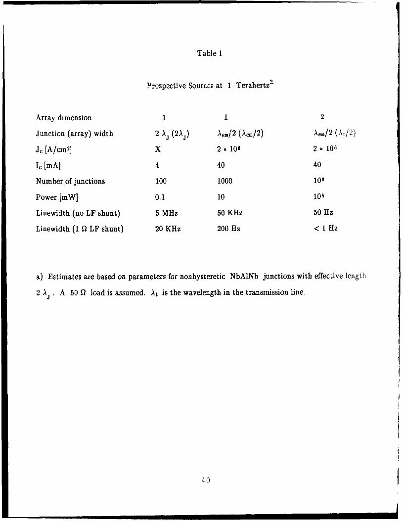
Table 1
Prospective Sourca at 1 Terahertza
Array dimension 1 1 2
Junction (array) width 2 AJ (2A~) Aem/2 (AeuiI2) A em!2 (At/2)
J, [A/cm2I X 2 x106 2 x10⁶
1, [mA] 4 40 40
Number of junctions 100 1000 106
Power [mW] 0.1 10 104
Linewidth (no LF shunt) 5 MHz 50 KHz 50 Hz
Linewidth (10~i LF shunt) 20 KHz 200 Hz < 1Hz
a) Estimates are based on parameters for nonhysteretic NbAINb junctions with effective length
2 A A 50 0) load is assumed. At is the wavelength in the transmission line.
40

Figure Captions
Fig. 1. a) Equivalent circuit model for resistively shunted junctions (RSJ) with biascurrent Ib, noise current I., shunt resistance R and capacitance C and supercurrent
Is = Icsin. b) Equivalent circuit for frequencies near vo.
Fig. 2. Diagram of in-line junction. a) Edge view showing Jc(x) concentrated
within 2A of end of junction. b) Top view. Tunnel barrier is enclosed by dashed lines.
Regions of non-zero tunneling current are shown by o
Fig. 3. Properties of single junction sources design for maximum available power at
a given frequency subject to the width constants w = 2 A (-- - narrow) and
w = 0.5 Aem (- wide), and for both cases J, = 105A/cm 2 and length is 2 A 2,am.
For narrow junctions the frequency independent values of I and w are indicated on the
axes (- - -). The available power of the wide junction is also frequency independent as
shown on the power axis.
Fig. 4. a) High frequency equivalent circuit for a one-dimensional array.
b-d) Possible junction connections for two-dimensional arrays.
Fig. 5. Equivalent circuit for the RSJ model from perturbation theory. Low
frequency (LF) section models response for w,,wj (wJ = 2rV/Do) and is coupled tc the
high frequency (HF) section by the mixing current Im - see text. HF section contains
the Josephson oscillator V lcosw t and source impedance Rj. The perturbation consists
of an rf current IT with w,,,w flowing through the HF terminals.
Fig. 6. a) Junction I-V curve in neighborhood of radiation induced step. b) Phase-
locking stability along step, [09/oIM]- . Note greatest stability is for 50 = 7r/2 . The
region 0>60>-7r is unstable.
Fig. 7. Equivalent HF circuit for an array terminated in load Z
Fig. 8. Relative phase of the mean oscillator voltage (real axis), load current 11 and
kth junction with different bias or critical current for array modeled in Fig. 7. Hatched
region is unstable.
Fig. 9. LF and HF equivalent circuit of junctions coupled in linear array showing
LF shunt R, and HF coupling load ZL.
Fig. 10. Power (A) and line width (o) as a function of junction number for a low
impedance (, 50 Q) 1-D array of nicrobridge junctions. vo = 10 GHz, Z = 50 0.
Fig. 11. a) HF equivalent circuit of a junction with a capacitor for perturbation.
b) Equivalent circuit as seen by the rest of the array.
Fig. 12. Relative phases of the oscillators, loop current It and locking current I
for an array of capacitive junctions.
Fig. 13. Layout of distributed array. Oscillator junctions (x) are placed at
wavelength intervals along the serpentine microstrip. Load resistor and detector junction
to monitor the load current are shown at upper left.
Fig. 14. RF current in transmission line (as measured by detector locking range) vs.
average frequency junctions in array.
Fig. 15. a) Micrograph of distributed array. b) Blowup of a), top left, showing
detector junction, load resistor and several oscillator junctions on the right. The vertical
separation of the oscillators is 10 pm.
Fig. 16. Power delivered to 23 f2 load resistor vs. array frequency for 40 junction
array. Junction parameters Ic = 2.5mA, R = 0.5 Q.
4?

(a)
I N I I
I I F? I Cb N OJ
(b)
V4

-2XJHt'IJ
(b)
I seel
F ig. 2
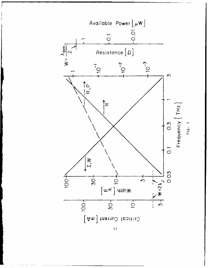
Available Power[,tWJ
- 6 0Ea
1< Resistance [Q]i
0 00
rO >
o 0 0r
0 0 0IC0 )
[Vw] uaiino looijjo
45
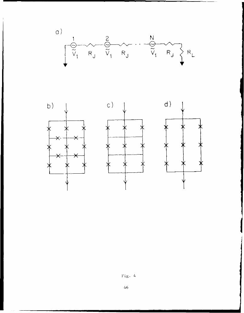
v )
10 10
Fig. 4
46
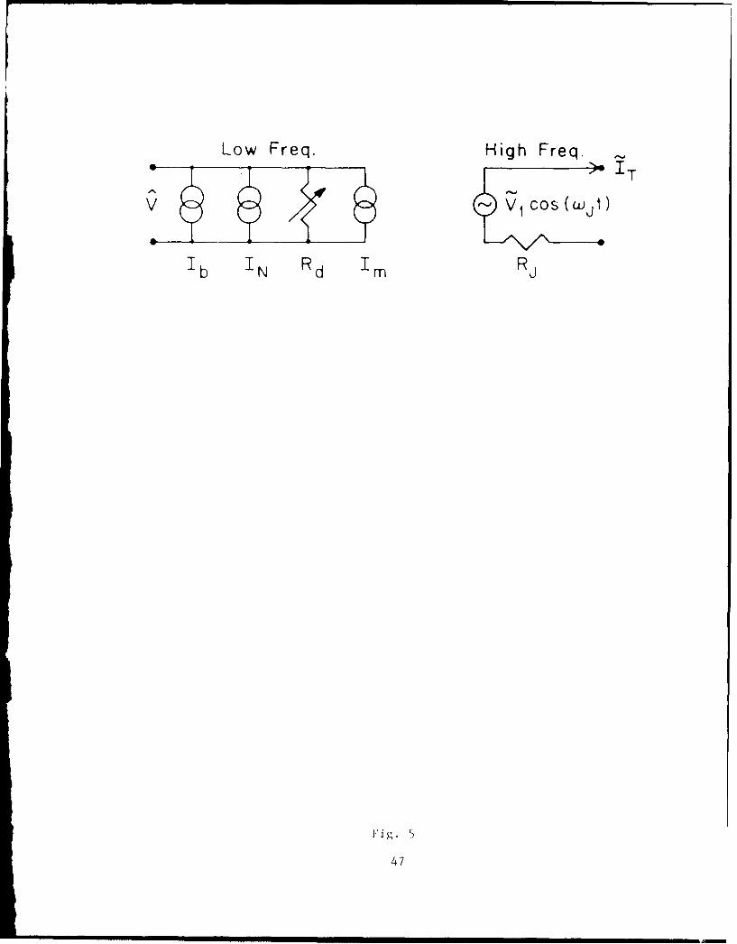
Low Freq. High Freq.
V v- I Cos (w31
'b N Rd mRJ
47
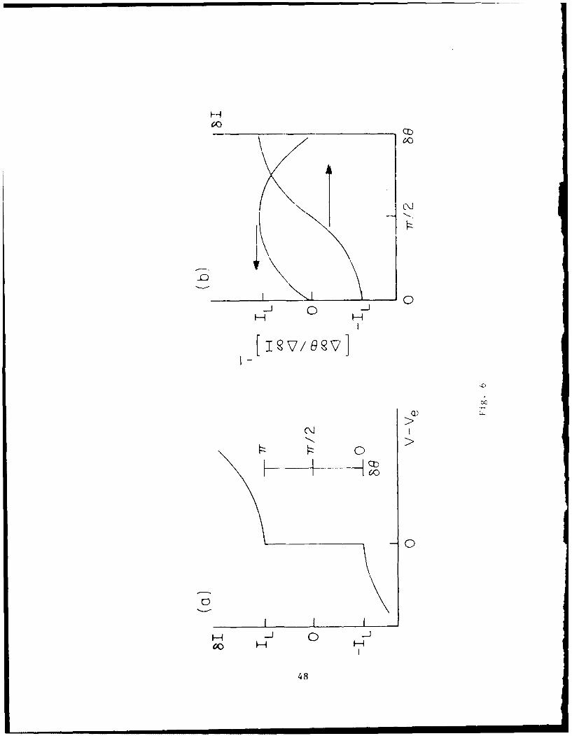
-DD
0co
48H
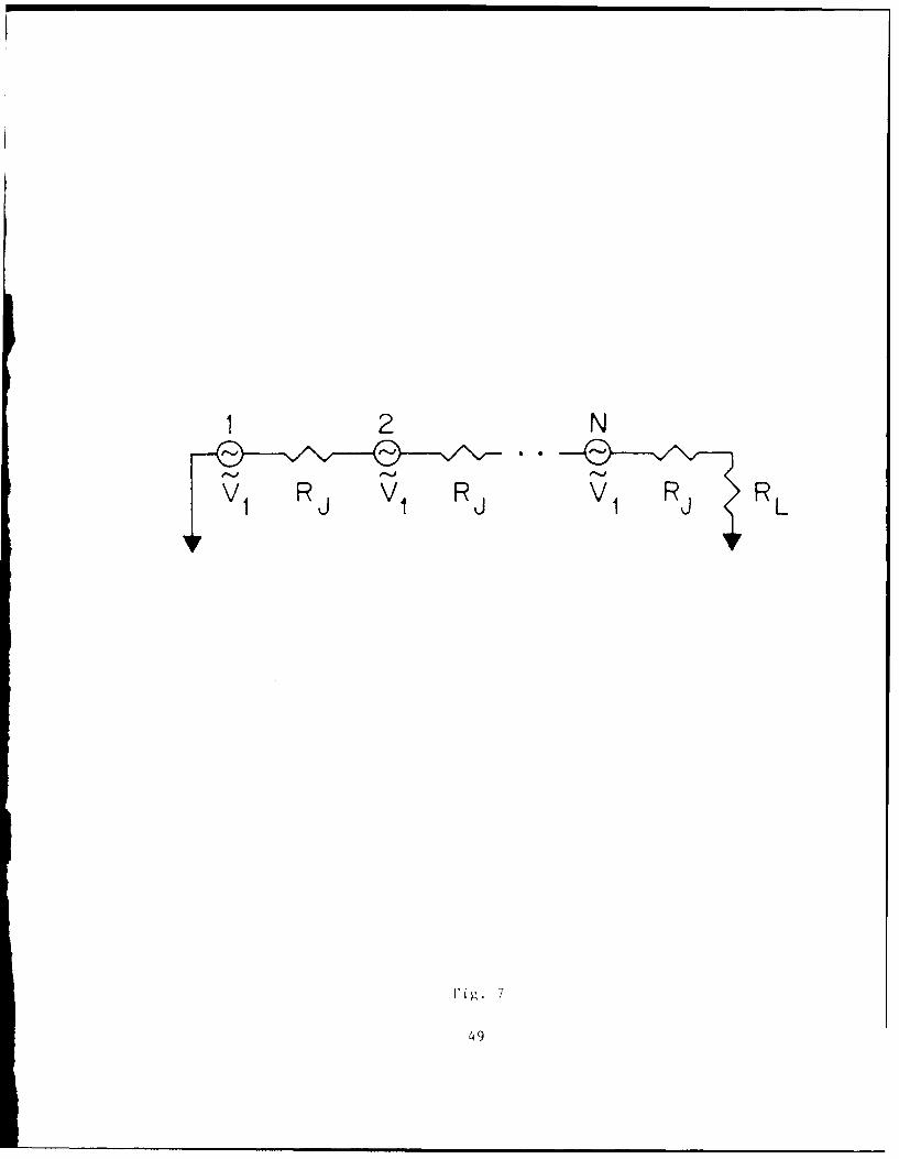
49
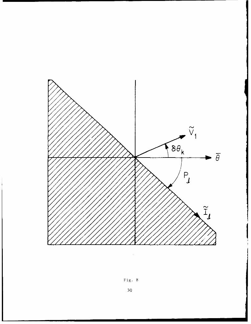
Fig. 8
50
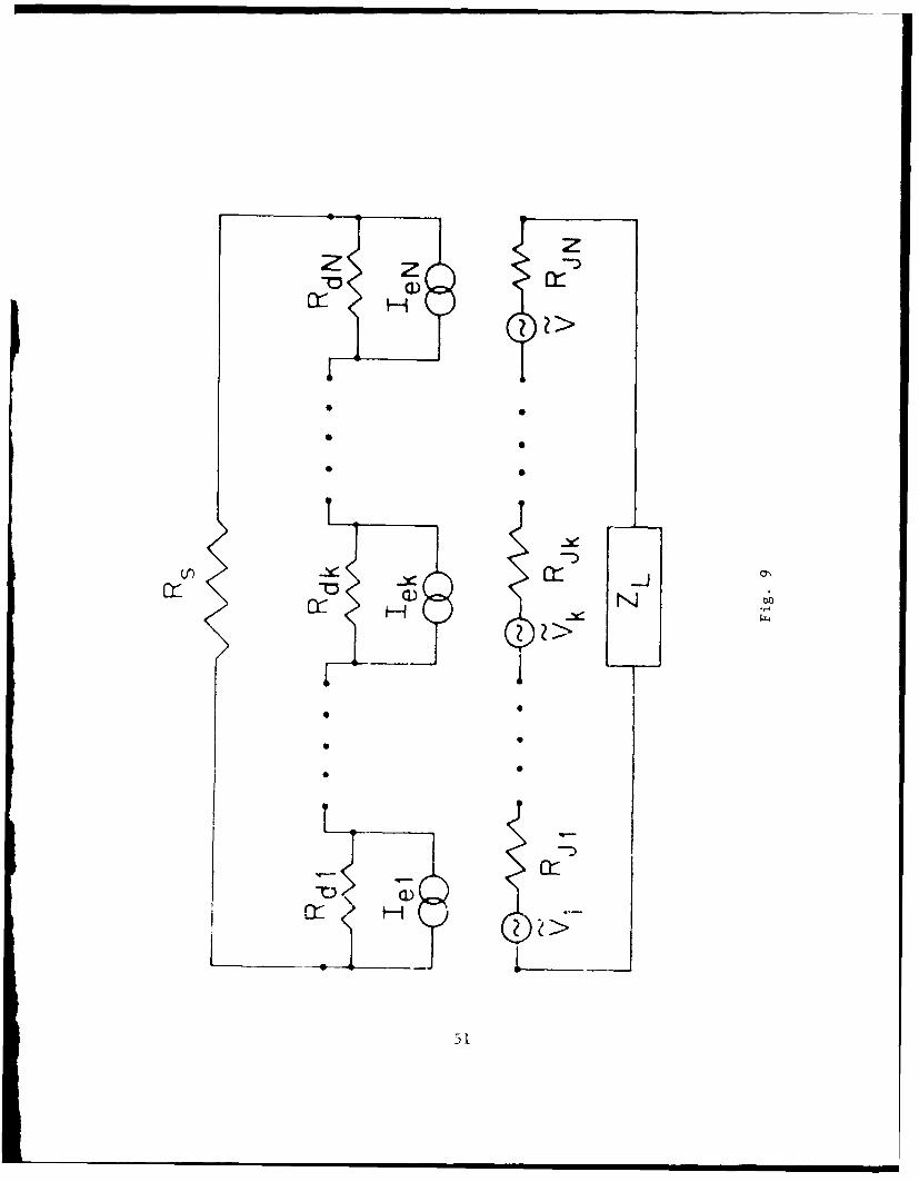
z2 -)
-~ a)cr: HI
0 0
00
0 0
(I) -~
-ocrc I-H -~ N
I0
0
00
00
~0
HI
51
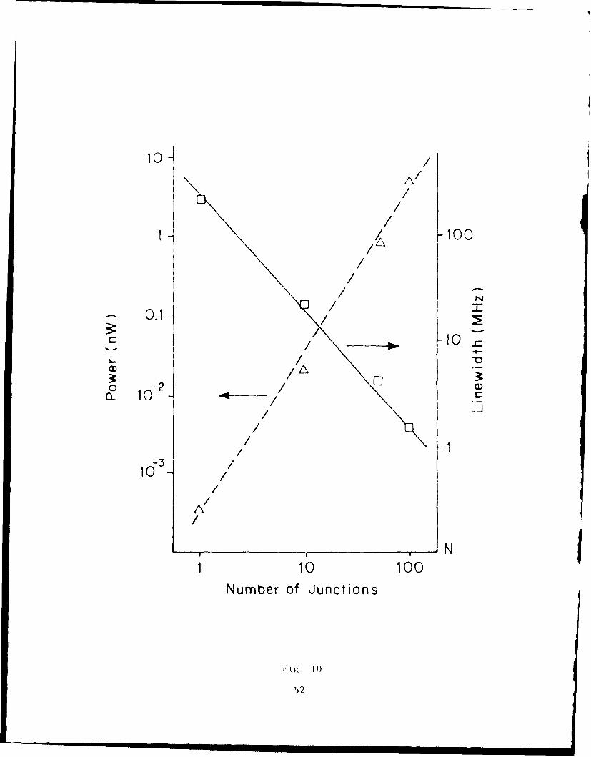
10 /
/ 100
/- N
0. // 10
-2 52

vi Ri
IRI
V1I 4 zi
Fig. 1 1
53
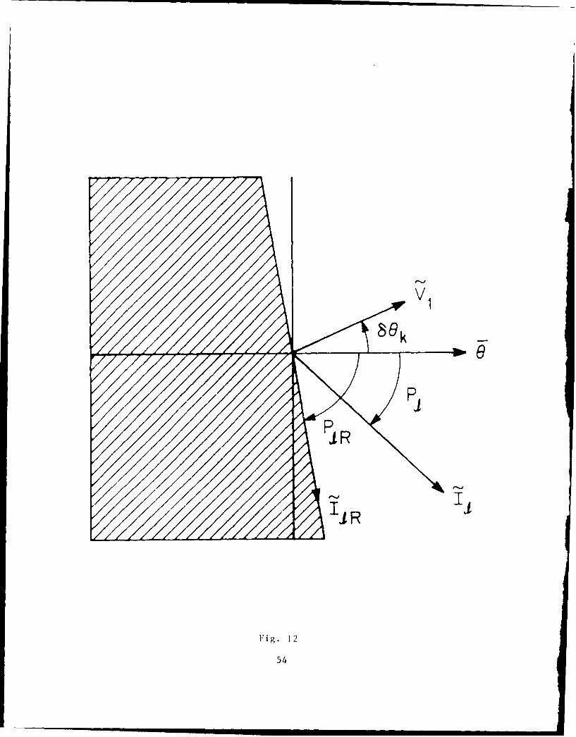
IRI
I I R
Fig. 12
54
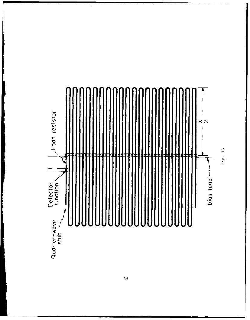
0
C)
Vl>/Du u
05
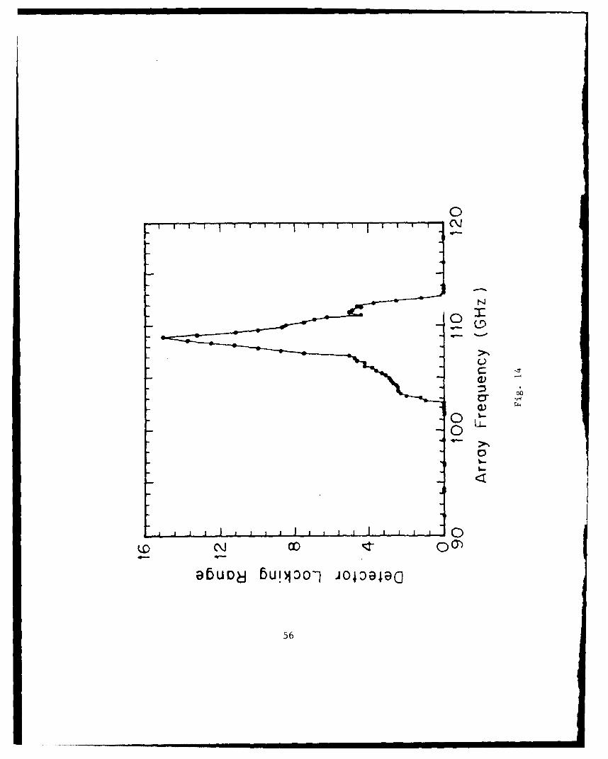
0
~0
00 ~ 0
ObUDd bUlMOO- Joloalc)
56

iTh
37
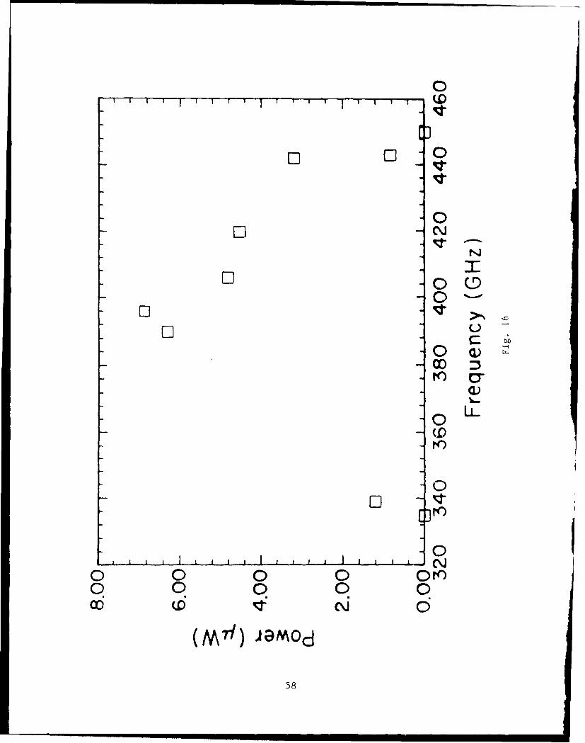
0
El I
00
C:
0)
0 LL
(0
0OEl(
I I I If I I ii i i
58

MISSIONof
Rome Air Development Center
RADC plans and executes research, development, test and
selected acquisition programs in support of Command, Control,
Communications and Intelligence (C3I) activities. Technical and
engineering support within areas of competence is provided to
ESD Program Offices (POs) and other ESD elements to
perform effective acquisition of C3 systems. The areas of
N' technical competence include communications, command and
S control, battle management information processing, surveillance
sensors, intelligence data collection and handling, solid state
sciences, electromagnetics, and propagation, and electronic
reliability/maintainability and compatibility.