study material - · pdf file · 2016-05-15cs6303 – computer architecture ......
TRANSCRIPT

CS6303 – COMPUTER ARCHITECTURE
“Chase Your Dreams; Dreams Do Come True” – Sachin Tendulkar
VI SEMESTER
PREPARED BY V.BALAMURUGAN, ASST.PROF/IT
STUDY MATERIAL
ANNA UNIVERSITY
REGULATION 2013
CS6303
COMPUTER ARCHITECTURE

CS6303 – COMPUTER ARCHITECTURE
“Chase Your Dreams; Dreams Do Come True” – Sachin Tendulkar
UNIT 1 – OVERVIEW AND INSTRUCTIONS PART – A
1. List the eight ideas invented by computer architects
Design for Moore’s Law
Use Abstraction to simplify Design
Make the common case fast
Performance via Parallelism
Performance via Pipelining
Performance via Prediction
Hierarchy of memories
Dependability via redundancy 2. What is pipelining? Pipelining is a set of data processing elements connected in series, where output of one element is the input of next element. 3. What are the major hardware components?
Input Unit (Keyboard, Mouse, etc.)
CPU (Memory Unit, ALU, Control Unit)
Output Unit (monitor, printer, speaker, etc.) 4. What is CPU and ALU? CPU: Central Processing Unit It is also called as brain of the computer Input and Output devices work according to the CPU ALU:- Arithmetic Logic Unit
It performs arithmetic and Logical operations
It is present inside the CPU
It uses main memory for operations (RAM) 5. What is control unit?
It is present inside the CPU
It controls the operation of input unit, output unit and ALU
It has the overall control of the computer
It tells memory unit to send/receive data
It tells ALU what operation to perform 6. What is Response Time and Throughput?
the time between the starting and ending of a task is called as response time. It is also called as “execution time”.
The total amount of work done in the given time is called as Throughput
7. What is CPU time?
Amount of time, the CPU spends for doing a task is called as CPU time
It is also called as CPU execution time
Time of waiting for I/O is not included.
𝐶𝑃𝑈 𝑡𝑖𝑚𝑒 =CPU time spent in program (user CPU time)
𝐶𝑃𝑈 𝑡𝑖𝑚𝑒 𝑠𝑝𝑒𝑛𝑡 𝑖𝑛 𝑂𝑆 (𝑠𝑦𝑠𝑡𝑒𝑚 𝐶𝑃𝑈 𝑡𝑖𝑚𝑒)
8. Write down the formula for power consumed by CPU. The formula for finding the power consumed by CPU is,
P = C V2 f Where,P=power, C=Capacitive loading, V=Voltage, f= frequency 9._What are multiprocessor systems? Give its advantages.
Computer systems that contain more than one processor are called as Multiprocessor systems
They execute more than one applications in parallel.
They are also called as shared memory multiprocessor s/m
High performance, high cost, high complexity. Advantages:-
Improved cost-performance ratio
High speed processing
If one processor gets failed, other processors will continue work.
10. _What is an instruction and instruction set?
Instruction is a part of code, written in step-by-step procedure for the CPU to complete a certain task
Instruction set is a set of instructions to be executed by the compiler, that contains all the details of the tasks
Ex for Instruction set:- Arithmetic instructions Ex: (ADD, SUB) Logic instructions Ex: (AND, OR, NOT) Data transfer instructions Ex: (MOVE, LOAD, STORE) Control flow instructions Ex: (GOTO, CALL, RETURN)
11. What is instruction format?
The format in which the instructions are written is called as Instruction format
Each instruction has three fields. OPCODE It specifies which operation is to be performed. MODE It specifies how to find effective address. ADDRESSIt specifies the address in memory/register
OPCODE MODE ADDRESS
12. What are the different logical instructions?
INSTRUCTION EXAMPLE Equivalent to
AND AND $1, $2, $3 $1 = $2 & $3
OR OR $1, $2, $3 $1 = $2 | $3
NOR NOR $1, $2, $3 $1 = ~ ($2 | $3)
ANDI AND $1, $2, imme $1 = $2 & imme
ORI OR $1, $2, imme $1 = $2 | imme
SHIFT LEFT SLL $1, $2, 10 $1 = $2 << 10
SHIFT RIGHT SRL $1, $2, 10 $1 = $2 >> 10
SHIRT RIGHT ARITHMETIC
SRA $1, $2, 10 $1 = $2 >> 10
13. Write the different control operations. Conditional branch:- BEQ instruction Branch on EQual ( BEQ $s, $t, offset) BNE instruction Branch on Not Equal (BNE $s, $t, offset) Unconditional branch:- J instruction Jump (J target) JAL instruction Jump And Link (JAL target) JR instruction Jump Register ( JR $s)
14. What is PC-relative addressing?
It is also called as Program Counter Addressing
The address of the Data or Instruction is specified as an offset, relative to the incremented Program counter.
It is used in conditional branches
Offset value can be direct or indirect value
Operand address = PC + Offset
Ex: BEQZ $t0, strEnd BEQZ = Branch if EQual to Zero
15. State Moore’s law
“Number of transistors per square inch, on Integrated Circuits (IC) had doubled every year since the IC was invented”
“Computer architects should concentrate on, after the design is finished, where the technology will be. Don’t bother where it has started”.
16. State Amdahl’s law
Improve the performance of common case, optimize rare case.
Use common case for designing non-frequent cases.
This method makes simple design and faster.
This idea is called as Amdahl’s law.
U
N
I
T
1

CS6303 – COMPUTER ARCHITECTURE
“Chase Your Dreams; Dreams Do Come True” – Sachin Tendulkar
PART – B 1. Explain the eight ideas invented by the architect for designing the computer system.
Design for Moore’s Law
Use Abstraction to simplify Design
Make the common case fast
Performance via Parallelism
Performance via Pipelining
Performance via Prediction
Hierarchy of memories
Dependability via redundancy
Design for Moore’s law:-
It is developed by Gordon Moore
He is the Co-founder of Intel
“Number of transistors per square inch, on Integrated Circuits (IC) had doubled every year since the IC was invented”
“Computer architects should concentrate on, after the design is finished, where the technology will be. Don’t bother where it has started”.
Moore’s law graph:- o “Up and to the Right” o Represent designing for quick change
Use abstraction to simplify the design:-
Abstraction means, hiding some part of the component.
It is used by the programmers and architects
It is used to represent the design at many levels.
At each level, its low level details are hidden.
This concept improves productivity
It simplifies the design
It reduces time for designing
Ex:- o In OS, I/O management details are hidden o In high level languages, sequence of
instructions are hidden.
Make the common case fast:-
Many big improvements in the performance of a computer come from the improvements in common case
Improve the performance of common case, optimize rare case.
Use common case for designing non-frequent cases.
This method makes simple design and faster.
This idea is called as Amdahl’s law.
Ex:- o It is easy to design a sports car from ordinary
car. o But it is not possible to design a sports car
from Van.
Performance via parallelism:-
Computer architects improves the performance by performing the operations in parallel.
A processor handles several activities simultaneously in the execution of an instruction.
Advantage: Faster performance of CPU.
Performance via pipelining:-
It is the extended concept of parallelism.
Pipeline is a set of data processing elements connected in series, where the output of one element is the input for the next element.
Elements that are independent from pipeline are executed in parallel to improve their performance.
Performance via prediction:-
Nowadays, processors reduce the bad effects of branches.
Predict the output of a condition
Test and start executing the indicated instruction
It is better than waiting for a correct answer.
If the prediction is accurate, performance is improved
Hierarchy of memories:-
Programmers need the memory to be fast, large and cheap.
Cache is a small memory for having recently used data.
Memory hierarchy used:- Top – to - bottom
Speed Fast to slow Top
Bottom Cost Expensive
Size Smallest to largest
In-board storage
Registers
Cache
Main Memory
Out-board storage
Magnetic disk (CD, DVD,
BluRay)
Off – line storage
Magnetic tapes
Dependability via redundancy:-
This idea is expensive
It uses RAID concept
RAID – Redundancy Array Inexpensive Disk
In RAID, data is stored redundantly on multiple disks
If one disk fails, other systems will continue working 2. State the CPU performance equation and discuss the factors that affect performance. CPU performance equation:-
CPU performance equation is defined as the ratio of product of (Instruction Count and no. of steps to execute one instruction) to the clock rate
T = N x S R
Where, T = CPU Execution time / Program Execution Time
N = No. of instructions
S = No. of steps to execute one instruction
R = Clock rate
Small, fast,
costly
Large, Slow,
Cheap

CS6303 – COMPUTER ARCHITECTURE
“Chase Your Dreams; Dreams Do Come True” – Sachin Tendulkar
Speed:-
To measure the performance of the computer It is used to measure how quickly a computer executes
programs.
Response time:-
Time between the starting and ending of a task
It is measured in seconds per program.
It includes disk access, memory access and I/O activities.
It is also called as execution time, wall-clock time, elapsed time
Throughput:-
Total amount of work done in a given time.
If response time is decreased, throughput is decreased. Increase the speed:-
To increase the speed of a computer:- o Decrease the response time o Increase the throughput
To decrease response time and increase throughput:- o Use the faster version of processors o Add extra number of processors
Relation between performance and execution time:- Performance = ______1______ Execution time
Let X and Y be two different computers, Performance x > Performance y
____1______ > ______1_______ Execution time x Execution time Y
Execution time Y > Execution time X
CPU time:- Amount of time, CPU spends for doing a task is called as CPU
time
It is also called as CPU execution time
Time of waiting for I/O is not included.
𝐶𝑃𝑈 𝑡𝑖𝑚𝑒 =CPU time spent in program (user CPU time)
𝐶𝑃𝑈 𝑡𝑖𝑚𝑒 𝑠𝑝𝑒𝑛𝑡 𝑖𝑛 𝑂𝑆 (𝑠𝑦𝑠𝑡𝑒𝑚 𝐶𝑃𝑈 𝑡𝑖𝑚𝑒)
Ex:- Given:- User CPU time = 90.7 sec System CPU time = 12.9 sec Elapsed time = 2 min 39 sec ( 159 sec) Find:- CPU time = ___90.7 + 12.9__ = 0.65 159
Performance equation – 1
CPU execution time = CPU clock cycles X clock cycle time
Clock rate is inverse of clock cycle time
Clock rate =______1______ Clock cycle time
CPU execution time = ____CPU clock cycles___ Clock rate
Performance can be improved by reducing length of the clock cycle or number of clock cycles
Execution time depends upon number of instructions in a program.
CPU clock cycles = Instructions X average clock cycles per instruction
CPI = average no. of clock cycles taken by each instruction for execution. Where, CPI = Clock cycles Per Instruction
Performance equation – 2 CPU execution time = Instruction Count x CPI x Clock cycle time CPU execution time = ____IC x CPI___ Clock rate Power equation:-
If performance is increased, clock speed is also increased.
If clock speed is increased, heat is also increased.
If heat is increased, power consumption is also increased.
Formula for power consumed by CPU:- P = C V2 f
Where=power, C=Capacitive loading, V=Voltage, f= frequency 3. What is instruction format? What are the types of instructions available?
The format in which the instructions are written is called as Instruction format
Some specific rules has to be followed while writing the instructions.
Each instruction has three fields. OPCODE It specifies which operation is to be performed. MODE It specifies how to find effective address. ADDRESSIt specifies the address in memory/register
OPCODE MODE ADDRESS
Types of instructions:-
Three address instructions
Two address instructions
One address instructions
Zero address instructions Three address instructions:-
Three Addresses of three registers are mentioned
Bits are required to specify three addresses of three operands
Bits are required to specify the operation
Syntax: Operation Destination, source1, source2.
Ex: ADD A, B, C
This Instruction adds B+C and stores in A ( A B + C)
Where, ADD operation, A destination, B,C Source
More execution time taken because of three addresses. Two address instructions:-
Two Addresses of two registers are mentioned
Bits are required to specify two addresses of two operands
Bits are required to specify the operation
Syntax: Operation Destination, source.
Ex: ADD A, B
This Instruction adds A+B and stores in A ( A A + B)
Where, ADD operation, A destination, B Source
Less execution time than three address instructions. One address instructions:-
One Address of one register is mentioned
Bits are required to specify one address of one operand.
Bits are required to specify the operation
Syntax: Operation Destination (or) Operation Source
Lesser execution time than two address instructions Ex: ADD A
This instruction adds the contents of Register A and Accumulator(A A + AC)
Where, ADD operation, A destination
operand acts as Destination
Ex: LOAD A
This instruction loads the contents of Register A into Accumulator(AC A)
Where, ADD operation, A source
operand acts as source

CS6303 – COMPUTER ARCHITECTURE
“Chase Your Dreams; Dreams Do Come True” – Sachin Tendulkar
Zero address instruction:- It contains no address fields
Source and destination operands are mentioned implicitly
Absolute address of the operand in a special register is automatically incremented of decremented
Top of the Pushdown stack is pointed. Bits are required to represent operation only. Syntax : Operation
Ex: ADD
Very less execution time than one address instructions.
4. What is logical instruction? Explain some logical instructions with examples each. Instructions that perform logical operations which manipulate
Boolean values are called as Logical instructions.
INSTRUCTION EXAMPLE Equivalent to
AND AND $1, $2, $3 $1 = $2 & $3
OR OR $1, $2, $3 $1 = $2 | $3
NOR NOR $1, $2, $3 $1 = ~ ($2 | $3)
ANDI AND $1, $2, imme $1 = $2 & imme
ORI OR $1, $2, imme $1 = $2 | imme
SHIFT LEFT SLL $1, $2, 10 $1 = $2 << 10
SHIFT RIGHT SRL $1, $2, 10 $1 = $2 >> 10 shirt right arithmetic SRA $1, $2, 10 $1 = $2 >> 10
AND instruction:- It contains three register operands
Syntax: Operation, destination, source1, source2
Ex: AND $1, $2, $3
It performs Bitwise-AND operation between source1 and source2 and stores the result in Destination.
It is equivalent to $1 = $2 & $3
OR instruction:- It contains three register operands
Syntax: Operation, destination, source1, source2
Ex: OR $1, $2, $3
It performs Bitwise-OR operation between source1 and source2 and stores the result in Destination.
It is equivalent to $1 = $2 | $3
NOR instruction:- It contains three register operands
Syntax: Operation, destination, source1, source2
Ex: NOR $1, $2, $3
It performs Bitwise-NOR operation between source1 and source2 and stores the result in Destination.
It is equivalent to $1 = ~($2 | $3)
ANDI instruction:- It contains three register operands
Syntax: Operation, destination, source1, source2
Ex: ANDI $1, $2, imme
It performs Bitwise-AND operation between source registers and immediate values.
It stores the result in Destination register. It is equivalent to $1 = $2 & imme
ORI instruction:- It contains three register operands
Syntax: Operation, destination, source1, source2
Ex: ORI $1, $2, imme
It performs Bitwise-OR operation between source registers and immediate values.
It stores the result in Destination register. It is equivalent to $1 = $2 | imme
Shift Left Logical Instruction:- It contains two register operands
Syntax: Operation, destination, source1, constant Ex: SLL $1, $2, 10
It shifts the value of $2 register Left side by 10 places
Extra Zeroes are shifted in. It stores result in destination $1
It is equivalent to $1 = $2 << 10
Shift Right Logical Instruction:- It contains two register operands
Syntax: Operation, destination, source1, constant Ex: SRL $1, $2, 10
It shifts the value of $2 register right side by 10 places
Extra Zeroes are shifted in. It stores result in destination $1
It is equivalent to $1 = $2 >> 10
Shift Right Arithmetic Instruction:- It contains two register operands
Syntax: Operation, destination, source1, constant Ex: SRA $1, $2, 10
It shifts the value of $2 register right side by 10 places
Sign bit is shifted in. It stores result in destination $1
It is equivalent to $1 = $2 >> 10
5. What is addressing mode? Explain the types of addressing modes.
Register addressing mode
Absolute addressing mode (or) Direct mode
Immediate addressing mode
Indirect addressing mode
Index addressing mode
Relative addressing mode
Auto increment mode
Auto decrement mode Register addressing mode:-
It is the simplest addressing mode
Both the operands are registers.
It is much faster than other addressing modes
Because they do not contact any other memory
The name of the register is mentioned in the instruction.
Ex: ADD R1, R2 (R1R1+R2)
Where, ADD operation, R1destination, R2 source
Registers
Absolute addressing mode:-
It is also called as direct addressing mode
Because the address of location of operand is given directly in the instruction.
Ex: MOVE A, 2000
This instruction copies the contents of memory location 2000 into the Register A.
Operand
Opcode Address

CS6303 – COMPUTER ARCHITECTURE
“Chase Your Dreams; Dreams Do Come True” – Sachin Tendulkar
Immediate addressing mode:-
The operand is given directly as a numerical value
It doesn’t require any extra memory access to fetch operand
It executes faster (immediate).
Ex: MOVE A, #20
JUMP instruction
The # symbol says that it is an immediate operand.
The value 20 is moved to the Register A
Ex: ADDI $t1, $0, 1
Where ADDI ADD Instruction Immediate $t1 operand $0 Register1, 1 Immediate value.
Indirect mode:-
It is also called as Register Indirect addressing mode.
Here, the address is not given directly
The memory address should be determined from the instruction
These addresses are called as Effective Address (EA)
The effective address of the operand is the contents of a register (or) the main memory location, whose address is given directly in the instruction.
When the effective address of the operand is the contents of a register, it is called as Register addressing Mode.
Ex: MOVE A, (R0)
It copies the contents of memory addressed by the contents of register R0 into the register A
Register given within the parenthesis ( ) is called as Pointer
A R0 2000
Index addressing mode:-
Indexing is a technique that allows programmer to refer the data (operand) stored in memory locations one by one.
In index addressing mode, the Effective address of the operand is generated by adding a constant value to the contents of a register
That constant is specified in the instruction
Ex: MOVE 20(R1), R2
It loads the contents of register R2 into memory location whose address is contents of R1 + 20
Where, MOVE operation, (R1) contents of R1, 20(R1) contents of R1 + offset 20, R2 source operand
R2 R1 1020 Relative addressing mode:-
It is also called as PC-Relative addressing mode
Because Program Counter is used in this mode.
Here, the effective address is calculated by the index mode using the program counter.
It is generally used in branch instructions
Operand address = PC + offset
Ex: BEQZ $t0, END
Where, $t0 Source operand,
Auto Increment mode:-
Here the effective address of the operand is the contents of a register specified in the instruction.
After accessing the operand, the contents of this register are incremented to address the next location.
Ex: MOVE (R2), + R0
The contents of R0 is copied into the memory location whose address is in the register R2
After copying, the contents of register R2 is automatically incremented by 1.
Auto decrement mode:-
The contents of the register is decremented by one and then it is used as the effective address of the operand.
Decrement operation for the register is done first, and then the instruction is continued.
Ex: MOVE R1, -(R0)
The contents of the address contained in R0 is decremented by one, and then it is moved to R1 register.
6. Assume two address format specified as source, destination. Examine the following sequence of instructions and explain the addressing modes used and the operation done in every instruction:- i) MOVE (R5)+, R0 ii) ADD (R5)+, R0 iii) MOVE R0, (R5) iv) MOVE 16(R5), R3 v) ADD #40, R5 Solution:- i) MOVE (R5)+, R0
Addressing mode: Auto increment addressing mode.
This instruction can be split as: MOVE (R5), R0 INCREMENT R5
This is also called as automatic post-increment mode.
Because, the increment is done after the operation
Operation: R5 is source, R0 is destination (given)
R5 contains some memory address. Go to that memory address and fetch the data from there.
MOVE it to Register R0
Then increment R5 ii) ADD (R5)+, R0
Addressing mode: Auto increment addressing mode.
This instruction can be split as: ADD (R5), R0 INCREMENT R5
This is also called as automatic post-increment mode.
Because, the increment is done after the operation
Operation: R5 is source, R0 is destination (given)
R5 contains some memory address. Go to that memory address and fetch the data from there.
ADD it to Register R0, and store in R0.
Then increment R5 iii) MOVE R0, (R5)
Addressing mode: Register indirect addressing mode
Because only registers are used in this instruction
And, one register is given indirectly within parenthesis.
R0 Source, R5 destination
The contents of R0 is moved to the memory location whose address is contained in R5.
10 2000 10
10 1000 10

CS6303 – COMPUTER ARCHITECTURE
“Chase Your Dreams; Dreams Do Come True” – Sachin Tendulkar
iv) MOVE 16(R5), R3
Addressing mode: indexed addressing mode
Operation:-
The 16th index position of R5 is moved to R3.
Effective address (EA) = (R5) + 16
R5
1(R5)
2(R5)
.
.
.
16(R5)
.
v) ADD #40, R5
Addressing mode: Immediate addressing mode
Operation:-
The # sign indicates that this is immediate operand
Here source #40, Destination R5 (given)
It Adds the value of operand 40 to the value of Register R5
And stores the result in R5
7. Explain the components of a computer system in detail. HARDWARE COMPONENTS:- The organization of a computer has four major parts. They are:-
o Input Unit
o CPU
o Output Unit
o Memory unit
Input Unit:-
Input devices get the data from the user and converts to
the machine understandable form.
Ex: Keyboard, Mouse, Scanner, Joystick, Light pen,
Card reader, Webcam, Microphone
Keyboard:-
It is a standard input device attached to all type of computers
It contains keys arranged in the form of QWERTY
It contains many keys such as TAB, CAPSLOCK, SPACE BAR, ALT, CTRL, ENTER, HOME, END, etc
It contains 101 to 104 keys
If we press the keys in the keyboard, electrical signals are sent to the computer.
Mouse:-
It is used with personal computer
Old type of mice have magnetic ball at the back.
Nowadays, Infrared mice are used, that works on infrared light at the back of the mouse.
Scanner:-
Keyboard can give input only the characters
Scanners can give a picture as input to the computer
Scanner is an optical device that takes a picture and gives as input to the computer
Ex: MICR, OMR, OCR
CPU:- It is called as brain of the computer
It performs takes such as arithmetic and logical operations
CPU is divided into three parts: ALU, Control Unit, Registers ALU:-
After the system gets input data, it is stored in primary storage.
The actual processing of data takes place at Arithmetic Logic Unit (ALU)
It performs addition, subtraction, multiplication, division, logical comparison, etc.
It also performs AND, OR, NOT, XOR, etc. operations Control Unit:-
It acts like the supervisor of a computer
It controls the overall activities of a computer components
It checks all the operations of a computer are going correctly or not.
It determines how the instructions are executed one by one
It controls all the input and output operations of a computer
For executing an instruction, it performs the following steps:- o Address of the instruction is placed in address bus o Instruction is read from the memory o Instruction is sent for decoding o Data from that address is read from the memory o These data and address are sent to the memory o Again the next instruction is taken from the memory
Registers:-
They are high speed memory units for storing temporary data
they are small in size
It stores data, instruction, address, etc.
ALU is also a register
Types: Accumulator, GPR, SPR( PC, MAR, MBR, IR)
Accumulator: to store the operands before execution. It receives the result of ALU operation
GPR: General Purpose Registers are used to store data and intermediate results
SPR: Special Purpose Registers used for certain purpose.
PC: Program counter, MAR: Memory Address Bus, MBR: Memory Buffer Register
R3
Moved to
Components of a computer
Hardware Software
System
Software
Appln
software
Program
Develop
ment
Envt
Java,
Games,
MS iffice,
etc
I/P
CPU =
ALU, CU
Memory
Unit O/p
Program
RunTime
Envt

CS6303 – COMPUTER ARCHITECTURE
“Chase Your Dreams; Dreams Do Come True” – Sachin Tendulkar
Memory Unit:- Primary storage:-
It is a part of CPU
Its storage capacity is limited
It contains magnetic core or semiconductor cells
It is used for temporary storage ROM:-
o Major type of memory in a computer is called ROM o Read Only Memory o It can be read, cannot be written o It is used for storing permanent values o ROM does not gets erased, even after the power is
switched off o They are non-volatile ( information cannot be erased) o We can store the important data into the ROM o Types: PROM, EPROM, EEPROM
RAM:- o They are used for storing programs and data that are
executed o It is different from ROM o Random Access Memory o It can be read and written o It is volatile o When the power is turned off, its contents are erased o It is also called as RWM (Read Write Memory) o It is faster than ROM o Static RAM (SRAM) and Dynamic RAM (DRAM) are
its types o Its cost is high o Its processing speed is also high
Cache memory:- o It is a very small memory used to store intermediate
results and data o It stores the data that are more frequently called. o It is present inside the CPU, near the processor o It is used for the faster execution
Secondary Storage:- o The speed of primary memory is fast, but secondary
memory is slow o But the memory capacity of primary memory is low. So,
secondary memory is used o It contains large memory space o It is also called as additional memory or auxiliary memory o Data is stored in it permanently o Ex: Magnetic tape, Hard disk, Floppy, Optical Disc, etc. Magnetic tape:- It is used for large computers like mainframe computers Large volume of data is stored for a long time It is like a old tape-recorder cassette They are cheap They store data permanently It is compact, low cost, portable, unlimited storage.
Optical Disk:- CD-ROM:
Compact Disk
They are made of reflective material
High power laser beam is passed to store data onto CD
Cost is low, storage capacity is 700MB
It can only be READ, can’t be written
Only a single side can be used for storage
Merits – CD Demerits - CD Large capacity compared to ROM Read only, cannot be updated
Cheaper, light weight Access is slow compared to magnetic disk
Reliable, removable and efficient It needs careful handling, easily get scratched
CD-RW:- o We can read and write data in that CD o Maximum capacity of 700MB o Light weight, reliable, removable, efficient o Lot of spaces wasted on outer tracks
DVD:
Digital Video Disk
It is the improved version of CD
Available in 4.7GB, 8.54GB, 9.4GB, 17.08GB
Both the sides are used for storage
They cannot be scratched or damaged like CD
We can store full movies, OS in one single DVD USB drives:-
They are commonly called as PEN DRIVES
They are removable storage
They are connected to the USB port of a computer
They are fast and portable
They store larger data when compared to CD, DVD (1GB to 64GB pen drives)
Hard disk:- Hard disks are disks that store more data and works faster It can store 10GB to 2TB It consists of platters; 2 heads are there for read and write It is attached to single arm Information in hard disk is stored in tracks
Floppy Disk They can store 1.4MB of data They are 5.25 to 3.5 inch in diameter They are cheap, portable
Output Unit:- It is a medium between computer and the human After the CPU finishes operation, the output is displayed in
the output unit Types of output:- Hardcopy, softcopy Hardcopy: The output that can be seen physically using a
printer is called as hardcopy Softcopy: The electric version of output that is stored in a
computer or a memory card, or a hard disk Ex: Monitor, Printer, Plotter Monitor:-
It is the most popular output device
It is also called as Visual Display Unit (VDU)
It is connected to a computer through a cable called Video cord
LCD: Liquid Crystal Display monitors o Flat screen- Liquid crystals are used for display
CRT: Cathode Ray Tube monitors o They are old-fashioned TV set like monitor
Printer:-
The output of a computer can be printed using Printer, to get the hardcopy
Laser printer, Inkjet printer: Impact printers. They give fast printouts with good quality using LASER
Dot matrix printer: non-impact printers. Their quality is poor, they are used for billing purpose

CS6303 – COMPUTER ARCHITECTURE
“Chase Your Dreams; Dreams Do Come True” – Sachin Tendulkar
Plotter:-
They are used for printing graphics
They are used in CAD/CAM
Pen plotters take printout by moving a pen across the paper SOFTWARE COMPONENTS 1.System Software
They are in-built within the computer system
They are essential for a computer to operate.
A computer cannot be run without them
They control and manage the hardware components Software for Program Development Environment:-
Text Editor: To type the program and make changes. Compiler: Converts High level language to machine code
Assembler: Converts Assembly level language to m/c code
Linker: Combines OBJ programs and creates EXE code
Debugger: To clear errors in EXE program
Software for RunTime Environment:- OS: It operates the overall computer system
Loader: Loads the EXE file into memory for execution
Libraries: Precompiled LIB files that are used by other pgrms
Dynamic Linker: Load and Link shared libraries at run time. 2. Application Software:-
They are softwares necessary for problem solving.
Programs such as JAVA, Games, MS-Word, Dictionary, Emulator, etc are the examples.
They are not necessary for a computer to operate.
They are optional; If user wants, he/she can install them.

CS6303 – COMPUTER ARCHITECTURE
“Chase Your Dreams; Dreams Do Come True” – Sachin Tendulkar
UNIT 3 – PROCESSOR & CONTROL UNIT
Part – A
1. How the performance of CPU is measured?
Instruction Count: It is determined by Instruction Set Architecture (ISA) and compiler.
Cycles Per Instruction (CPI) and Clock cycle time: It is determined by the CPU hardware
2. Write the basic performance equation of CPU
CPU time = Instruction count X CPI X Clock cycle (or)
CPU time = (Instruction count X CPI) / Clock Rate 3. What is MIPS?
Million Instructions Per Second
It is a metric used to measure CPU performance
It is defined as the ratio of Instruction count to the product
of execution time and 106
MIPS = Instruction count / (Execution time X 106) 4. What are the types of Instruction in MIPS instruction set?
Memory reference instructions : Load word (LW), store word (SW)
Arithmetic logical instructions : ADD, SUB, AND, OR, SLT
Control flow instructions : BEQ, JUMP 5. What are the steps involved in MIPS instruction execution?
Fetch instruction from memory
Decode the instruction
Execute the operation
Access an operand in Data memory
Write result into register 6. What is a data path?
Data path is the pathway that data takes through the CPU
Data travels through data path; control unit regulates it
It consists of functional units that perform ALU operations 7. What is PC?
Program counter is defined as a register which is used to store the address of the instruction in the program being executed
It is a 32 bit register, written automatically after end of clock cycle
No need of a WRITE control signal 8. What is pipelining? Mention its purpose and advantages
Pipelining is defined as the implementation technique in which more than one instruction is overlapped for simultaneous execution
It is used to make the processors fast
It is divided into stages; each stage finishes a part of execution in parallel
All stages are connected one to next one to form a pipe
It increases instruction throughput.
9. What are the stages of MIPS pipeline?
IF : Instruction fetch from memory
ID : Instruction Decode
EX : Execute the operation
MEM : Access the memory for an operand
WB : Write back the results in a register 10. Define hazard. Mention its types.
Any condition that makes pipeline to stall is called HAZARD
It avoids execution of next instruction in the instruction stream Structural hazard: Two instructions use same resource at same time
Data hazard: Data are not available at expected time in pipeline
Control hazard: branch decisions made before branch condition
11. What is data hazard? Mention its types.
Data hazard occurs when data are not available at expected time in a pipeline
Consider two instructions: I1 occurs before I2
RAW: Read After Write: I2 reads before I1 writes it
WAW : Write After Write : I2 writes before I1 writes it
WAR : Write After read: I2 writes before I1 reads it 12. What are the methods to handle Data hazard?
Forwarding: Result is passed forward from a previous instruction to a later instruction
Bypassing: Passing the result by register file to the desired unit
13. What are the methods to handle control hazard?
Stall the pipeline
Predict branch not taken
Predict branch taken
Delayed branch 14. Define an exception with Ex.
It is also called as interrupt
It is defined as an unscheduled event that disturbs the normal execution of the program
Ex:
ADD R1, R2, R1 R1 = R2 + R1
Arithmetic overflow has occurred
U
N
I
T
-
3

CS6303 – COMPUTER ARCHITECTURE
“Chase Your Dreams; Dreams Do Come True” – Sachin Tendulkar
Part - B 1. Explain the types of MIPS Instruction format. R-Format:-
Opcode Rs Rt Rd SHAMT FUNCT
31-26 25-21 20-16 15-11 10-6 5-0
Also called as Register format
Because only registers are used
Three register operands : Rs, Rt, Rd
Rs, Rt source register
Rd Destination
SHAMT Shift And Move To
FUNCT ALU functions (ADD, SUB, AND, OR, SLT)
Opcode for R-format = 0
ALU control lines Function
000 AND
001 OR
010 ADD
110 SUB
111 (SLT)Set on Less Than
I-Format:-
Opcode Rs Rt Address
31-26 25-21 20-16 15-0
For Load/Store instructions o For LOAD, Opcode = 35 o For STORE, opcode = 43 o Rs Base register o Rt For load, it is the destination register, for
store, it is the source register o Memory address = base register + 16 bit
address field
For Branch Instructions o For BRANCH, opcode = 4 o Rs, Rt source registers o Target address = PC + (sign-extended 16-bit
offset address << 2 ) J-Format:-
Opcode Address
31-26 25-0
For Jump instructions, Opcode = 2 Destination address = PC [31-28] | | (Offset address < < 2 )
2. Explain Datapath and its control in detail.
(Or) Explain Datapath and its control implementation schemes for MIPS instruction formats with neat diagrams. Data path:-
Data path is the pathway that data takes through the CPU
Data travels through data path; control unit regulates it
It consists of functional units that perform ALU operations Functional Units of data path:-
Instruction memory:-
It is a memory unit to store instructions of a program and supply instructions Program Counter:-
Program counter is defined as a register which is used to store the address of the instruction in the program being executed
Adder:-
Increment the PC to solve next instruction
An ALU is connected to perform addition of its two 32bit inputs, place result on its output Registers:-
It is a structure that contains processor’s 32 GPR
They can be read / Written
It contains 4 inputs (2 read ports + 1 write port + 1 writeData)
It contains 2 outputs (two read data) ALU:-
Input: two 32bits
Output: 32bit result Data memory Unit:-
Input: Address and write data
Output: Read result Sign extension Unit:-
Input: 16bit sign
Output: 32bit extended sign MUX:-
It is also called data selector
It allows multiple connections to the input of an element and have a control signal SELECT among the inputs.
Building a data path:- Fetch instructions:-
To execute any instruction, first the instruction is fetched from memory
To prepare for executing next instruction, PC is incremented by 4 bytes, which points to next instruction
Data path for R-Format instructions:-
Regiter File and ALU are needed additionally with previous components.
ALU gets input from DataRead ports of register File
Register file is written by ALUResult output of ALU with RegWrite signal

CS6303 – COMPUTER ARCHITECTURE
“Chase Your Dreams; Dreams Do Come True” – Sachin Tendulkar
Data path for Load/Store instructions:- Data memory unit and Sign extension unit are needed additionally
Three register inputs are read from instruction field
Memory address is calculated based on instruction field For Load, data at memory address is read from data memory
For store, write data is written into data memory Data path for Branch/Jump instructions
Branch target = Incremented PC + sign-extended, lower 16bits of instruction, shift left 2 bits
Compare register contents using ALU
Combining data paths for simple implementation:-
ALU control lines Function
000 AND
001 OR
010 ADD
110 SUB
111 (SLT)Set on Less Than
Opcode
ALUop
Operation
FUNCT
ALU action
ALU control input
LW 00 Load Word
Xxxxxx Add 010
SW 00 Store word
Xxxxxx Add 010
BEQ 01 Branch on Equal
Xxxxxx Sub 110
R-Type 10 ADD 100000 Add 010
R-type 10 SUB 100010 Sub 110
R-Type 10 AND 100100 AND 000
R-Type 10 OR 100101 OR 001
R-Type 10 Set On Less Than
101010 SLT 111
Truth Table for Three ALU control bits:-
ALUop FUNCT field Operation ALUop1 ALUop2 F5 F4 F3 F2 F1 F0
0 0 X X X X X X 0010
X 1 X X X X X X 0110
1 X X X 0 0 0 0 0010
1 X X X 0 0 1 0 0110
1 X X X 0 1 0 0 0000
1 X X X 0 1 0 1 0001
1 X X X 1 0 1 0 0111
Control Signals used in Control implementation:-
Signal When RESET (0) When SET (1)
RegDst Destination Register Number comes from
Rt
Destination Register Number comes from
Rd
RegWrite None Register on Write register input is written
with value of Write Data input
ALUsrc Second ALU operand comes from 2nd register file o/p
2nd ALU operand is sign-extended, lower 16bits of instruction
PCsrc PC replaced by o/p of adder that calculates
PC+4
PC is replaced by o/p of adder that
calculates branch target
MemRead None Data memory contents designated by address input are put on Read
data o/p
MemWrite None Data memory contents designated by address input are replaced by
value on Write data i/p
MemtoReg Value fed to register write data i/p comes
from ALU
Value fed to register write data i/p comes from data memory
t

CS6303 – COMPUTER ARCHITECTURE
“Chase Your Dreams; Dreams Do Come True” – Sachin Tendulkar
AL
Uo
p
0 0 0 0 1
AL
Uo
p
1 1 0 0 0
Bra
nc
h
0 0 0 1
Mem
Wri
te
0 0 1 0
Mem
Rea
d
0 1 0 0
Reg
Wri
te
1 1 0 0
Mem
to
Reg
0 1 X
X
AL
Usr
c 0 1 1 0
Reg
Ds
t 1 0 X
X
Inst
ru
ctio
n
R-
form
at
LW
SW
BE
Q
Data path : R-Type:-
Fetch instruction and increment PC
Get operands from register file, based on Src reg num
Perform ALU operation using ALUSrc=0
Select o/p from ALU using MemtoReg=0
WB to destination register(regWrite=1, RegDst=1) Data path : Memory access (Load):-
Fetch instruction and increment PC
Get base register operand from reg file
Perform addition of register value with ALUsrc=1
Use ALU result as address for data memory
Use MemtoReg = 1 to select read data and WB to destination register using RegWrite=1, RegDst=0

CS6303 – COMPUTER ARCHITECTURE
“Chase Your Dreams; Dreams Do Come True” – Sachin Tendulkar
Data path : memory access (store):-
Fetch instruction and increment PC
Get base register and data from register file
Perform addition of register value with ALUsrc=1
Use ALU result as address for data memory
Using MemWrite=1, write data operand to memory address Data path : branch:-
Fetch instruction and increment PC
Read 2 registers from register file for comparison
ALU subtracts data values using ALUsrc=0
Generate branch address: add PC+4, shift left by 2
Use zero o/p from ALU to find which result to be used for updating PC
If equal, use branch address
Else, use incremented PC
Data path : Jump:- Shift instruction bits 25-0 left two bits to create 28bit value
Combine with 31-28 bits of PC+4 to get 32bit jump addr
Additional MUX uses Jump control to select instruction address
0: incremented PC (or) Branch target
1: Jump address 3. What is pipelining? Explain its stages with an example.
Pipelining is defined as the implementation technique in which more than one instruction is overlapped for simultaneous execution
Purpose:-
It is used to make the processors fast
It is divided into stages; each stage finishes a part of execution in parallel
All stages are connected one to next one to form a pipe Advantage:-
It increases instruction throughput. Example:- Consider the following instructions:- LW R1,100(R0) LW R2, 200(R0) LW R3, 300(R0) Without pipeline:-

CS6303 – COMPUTER ARCHITECTURE
“Chase Your Dreams; Dreams Do Come True” – Sachin Tendulkar
With pipeline:- Stages of pipeline:-
IF : Instruction fetch from memory
ID : Instruction Decode
EX : Execute the operation
MEM : Access the memory for an operand
WB : Write back the results in a register Graphical representation:- 4. Explain the types of hazards with examples.
Structural hazard
Data hazard
Control hazard Structural hazard:-
It occurs when two instructions use same resource at the same time
Here, 1st instruction is accessing data from memory, 4th instruction is fetching an instruction from that same memory at the same time.
Time CC1 CC2 CC3 CC4 CC5 CC6 CC7 CC8 Instr1 IF ID Ex MEM WB
IF ID Ex MEM WB
IF ID Ex MEM WB
IF ID Ex MEM WB
Data hazard:-
It occurs when data are not available at the expected
time in the pipelined execution.
Consider two instructions: I1 occurs before I2
RAW
Read After Write
I2 reads before I1 writes it
So, I2 gets incorrect value
WAW
Write After Write
I2 writes before I1 writes it
I1 modifies the value, so I2 gets incorrect value
WAR
Write After read
I2 writes before I1 reads it
So I1 incorrectly reads the read value
Handling data hazard:- (solutions) Forwarding Bypassing Control hazards:-
It is also called branch hazard
It occurs when branching decision made before branch Handling control hazard:- (solutions) Stall the pipeline:- Predict branch not taken:-

CS6303 – COMPUTER ARCHITECTURE
“Chase Your Dreams; Dreams Do Come True” – Sachin Tendulkar
Predict branch taken:- Delayed branch:- 5. Explain the pipelined data path and its control. Stages of pipeline:-
IF : Instruction fetch from memory
ID : Instruction Decode
EX : Execute the operation
MEM : Access the memory for an operand
WB : Write back the results in a register For Load instruction:- 1. Instruction Fetch (IF)
Read instr’n from memory using address in PC
Place the fetched instr’n in IF/ID pipelined register
Increment the PC contents by 4 (PC PC + 4) 2. Instruction Decode (ID)
IF/ID pipeline registers supply two registers to be read
Read data from those two registers
Store them in ID/EX pipeline register 3. Execute instruction (EX)
Read reg1 contents from ID/EX pipeline register
Add them using ALU
Place the sum in EX/MEM pipeline register 4. Memory access (MEM)
Read data memory using address from EX/MEM pipeline
Load data into MEM/WB pipeline register 5. Write Back (WB)
Read data from MEM/WB pipeline register
Write it into register file
Instruction fetch:-
Instruction decode:-

CS6303 – COMPUTER ARCHITECTURE
“Chase Your Dreams; Dreams Do Come True” – Sachin Tendulkar
Instruction Execution:- Memory access:-
Write Back:- For Store instruction:- 1. Instruction Fetch (IF)
Read instr’n from memory using address in PC
Place the fetched instr’n in IF/ID pipelined register
Increment the PC contents by 4 (PC PC + 4) 2. Instruction Decode (ID)
IF/ID pipeline registers supply two registers to be read
Read data from those two registers
Store them in ID/EX pipeline register 3. Execute instruction (EX)
Read reg2 contents from ID/EX pipeline register
Add them using ALU
Place the sum in EX/MEM pipeline register 4. Memory access (MEM)
Read data memory
store data into ID/EX pipeline register 5. Write Back (WB)
No process is done (Diagrams: Same as above for load instructions)

CS6303 – COMPUTER ARCHITECTURE
“Chase Your Dreams; Dreams Do Come True” – Sachin Tendulkar
UNIT 4 – PARALLELISM
PART – A 1.. Distinguish between strong scaling and weak scaling.
Strong scaling Weak scaling
Strong scaling means, at a constant problem size, the parallel speed up increases linearly with the number of processors used.
Weak scaling means, the time to solve a problem with increasing size can be held constant by enlarging the number of processors used.
It is limited by Amdahl’s law.
It is limited by memory.
2.. Distinguish between UMA and NUMA
UMA NUMA
It is a type of shared memory architecture.
It is a type of shared memory architecture.
All the processors are identical, connected to a network, have equal access to all memory regions.
All the processors are identical, connected to a network, have individual memory units attached to it.
They are also called as Symmetric Multi-Processor machines (SMP).
They are also called as Asymmetric Multi-Processor machines (AMP)
. . . . . . . . . . .
. . . . . . . . . .
3.. What is Flynn’s classification?
Flynn has classified parallel computer architectures based on number of concurrent instructions and data streams
They are: SISD, SIMD, MISD, MIMD
Name Full form No.of processor
No.of instruction
No.of data stream
SISD Single Instruction Single Data
1 1 1
SIMD Single Instruction
Multiple Data
N 1 N
MISD Multiple Instruction Single Data
N N 1
MIMD Multiple Instruction
Multiple Data
N N N
4.. Define Multi-threading.
The ability of a CPU or a processor to execute multiple processes or threads concurrently is called as Multi-threading
It allows multiple threads to share the functional units of a single processor in overlapped fashion.
5. Define parallelism. What are its goals? Mention its types.
Parallelism is defined as the process of doing multiple operations at the same time.
Goals:- o Speed up the processing, increase the speed. o Increase the throughput o Improve the performance
Types:- o Instruction level parallelism o Task parallelism o Bit-level parallelism
6. What is ILP? What are the approaches to exploit ILP?
The technique which is used to overlap the execution of instructions and improve performance is called as Instruction-Level-Parallelism
Approaches:- o Dynamic hardware intensive approach o Static compiler intensive approach
7. Define Loop level Parallelism
The common way to increase the amount of parallelism available among instructions is, to exploit parallelism among iterations of a loop. This is called as Loop-level parallelism.
8.. What are the types of dependencies?
Data dependence
Name dependence
Control dependence
9. What are the types of Data hazard?
RAW (Read After Write)
WAW (Write after Write)
WAR (Write after Read) 10.. Define IPC
Inter process communication is defined as a set of programming interfaces that allow a programmer to coordinate activities among different program processes that can run concurrently in an operating system.
It allows the program to handle many user requests concurrently.
11.. Mention the three ways to implement Hardware MT
Coarse-grained Multi-threading
Fine-grained multi-threading
Simultaneous Multi-threading (SMT) 12. Mention the advantages of multi-threading
To tolerate latency of memory operations, dependent instructions, etc.
To improve system throughput by exploiting TLP
To reduce context switch penalty 13. What are multi-core processors? Give its applications.
A multi-core processor is a single computing component that contains two or more distinct cores in the same package.
Applications: General purpose, embedded systems, Networks, Digital Signal Processing, Graphics.
Bus interconnection n/w
M M M
P P
Bus interconnection n/w
M M
P P
M
P
U
N
I
T
4

CS6303 – COMPUTER ARCHITECTURE
“Chase Your Dreams; Dreams Do Come True” – Sachin Tendulkar
.
.
.
.
.
.
.
.
PART – B 1. Explain the Flynn’s classification of parallel computer architectures with neat diagrams.
Flynn proposed a concept for describing a machine’s structure based on stream.
Stream means a sequence of items
There are two types of streams:- o Data stream (Sequence of Data) o Instruction stream (Sequence of instructions)
Flynn classified parallel computing architectures based on number of concurrent instructions and data streams
They are: SISD, SIMD, MISD, MIMD Name Full form No.of
processor No.of
instruction No.of data
stream
SISD Single Instruction Single Data
1 1 1
SIMD Single Instruction
Multiple Data
N 1 N
MISD Multiple Instruction Single Data
N N 1
MIMD Multiple Instruction
Multiple Data
N N N
SISD:-
Single Instruction Single Data
Each processor executes SINGLE instruction on a SINGLE data stream
Ex: IBM 704, VAX, CRAY – I Instruction stream
Instruction Data stream Stream
Advantages Disadvantages
Simple and easy to implement.
Low performance achieved
Less penalty will be levied. Low throughput is yielded
Less overhead will occur. Low level of parallelism exploited
SIMD:-
Single Instruction, Multiple Data
SINGLE instruction is executed on MULTIPLE data streams by multiple processors is called as SIMD
Ex: ILLIAC – IV, MPP, CM-2, STARAN
MISD:-
Multiple Instruction, Multiple Data
MULTIPLE INSTRUCTIONS are executed on SINGLE DATA streams by multiple processors
Ex: Pipelined Architecture
Advantages Disadvantages Better throughput than SISD High complexity
Less penalty than SISD High bandwidth required Better performance than SISD Low level of parallelism exploited
MIMD:-
Multiple Instruction, Multiple Data
MULTIPLE INSTRUCTIONS are executed on MULTIPLE DATA streams on multiple processors (CPUs)
Instruction stream Data stream
Instruction stream Data stream
Advantages Disadvantages Better throughput than MISD High complexity
Less penalty than MIMD Difficult to deploy and repair High level of parallelism exploited
Difficult to learn
2. What is multi-threading? Explain hardware multi-threading and its classification with illustrations Definition:-
The ability of a CPU or a processor to execute multiple processes or threads concurrently is called as Multi-threading
It allows multiple threads to share the functional units of a single processor in overlapped fashion.
Use:-
To increase the usage of existing hardware resources.
Memory Control Unit CPU
I/O
Control
Unit
CPU1
CPU2
CPU-N
Memory1
Memory2
Memory-n
.
.
.
.
CPU1
CPU2
CPU-N
Control Unit
Control Unit
Control Unit
Memory
Memory-1 Control Unit CPU
1
Memory-n Control Unit CPU
N
B U S INTERCONNECT IO
N

CS6303 – COMPUTER ARCHITECTURE
“Chase Your Dreams; Dreams Do Come True” – Sachin Tendulkar
Purpose:-
To tolerate latency of memory operations, dependent instructions, etc.
To improve system throughput by exploiting TLP
To reduce context switch penalty Three ways to implement HMT:-
Coarse-grained Multi-threading
Fine-grained multi-threading
Simultaneous Multi-threading (SMT) i) Coarse-grained multi-threading:-
When a thread is stalled due to some event, switch to a different hardware context. This is called as coarse-grained multi-threading
It is also called as switch-on-event multi-threading
Advantages:- o It eliminates the need to have very fast
thread-switching o It does not slow down the thread because
the instructions from other threads issued only when the thread faces a costly stall.
Disadvantages:- o Since the CPU issues instructions from one
thread, when a stall occurs, the pipeline must be emptied or frozen
o New thread must fill pipeline before instructions can complete
ii)Fine-grained multi-threading:-
Switch to another thread in every cycle, such that no two instructions from the thread are in pipeline concurrently
It improves the usage of pipeline by taking advantage of multiple threads
Advantages:- o No need to check dependency between
instructions because only one instruction is in pipeline from a single thread.
o No need for branch prediction logic o Bubble cycles are used for executing useful
instructions from different threads o Improved system throughput, latency,
tolerance, usage.
Disadvantages:- o Extra hardware complexity is created,
because many hardware contexts are there, many thread selection logic is there
o A single thread performance is reduced o Resource Conflicts are created between the
threads iii)Simultaneous Multi-threading(SMT):-
Intel introduced SMT in 2002 (Intel Pentium IV – 3.06GHz)
It uses resources of a dynamically scheduled processors to exploit ILP
At the same time, it exploits ILP, It converts TLP into ILP
It also exploits following features from latest processors: o Multiple functional units: latest processors
have more functional units for a single thread o Register renaming and dynamic
scheduling: multiple instructions from independent threads can co-exist and co-execute
Advantages:-
More threads execute concurrently
Best processor utilization is done.
High performance is achieved Disadvantages:-
Highly complex task for software developers to develop the software to implement SMT on the given hardware
Security problem is also there. Intel’s hyper-threading technology has a drawback. On a system with many concurrent processes, from one process, one can steal the login details which is running in another process.
Illustration:-
Superscalar Course-grained Fine grained SMT
Thread 1
Thread 2
Thread 3
idle
3. What is ILP? Explain the methods to enhance the performance of ILP. Definition:-
The technique which is used to overlap the execution of instructions and improve performance is called as Instruction-Level-Parallelism
Principle:-
There are many instructions in code that don’t depend on each other so it’s possible to execute those instructions in parallel.
Build compilers to analyse the code
Build hardware to be even smarter than that code Approaches:-
Dynamic and hardware intensive approach:- o It depends on hardware to exploit the
parallelism dynamically at run time. o It is used in desktop, server and in wide range
of processors. o Ex: Pentium III and IV, Athlon, MIPS
R10000/12000, Sun UltraSPARC III, PowerPC 603, Alpha 21264
Static and compiler intensive approach:- o It depends on software technology to find
parallelism statically at compile time. o It is used in embedded systems o Ex: Intel IA-64 architecture, Intel Itanium

CS6303 – COMPUTER ARCHITECTURE
“Chase Your Dreams; Dreams Do Come True” – Sachin Tendulkar
Methods to enhance performance of ILP:- i) LLP ii) Vector instructions
Loop-level parallelism:-
The common way to increase the amount of parallelism available among instructions is, to exploit parallelism among iterations of a loop. This is called as Loop-level parallelism.
Ex:- for ( i = 1; i < = 1000 ; i = i + 1 ) { x[i] = x[i] + y[i]; }
Every iteration of the loop overlap with any other iteration.
Within each loop iteration, there is less chance for overlap.
LLP means, parallelism existing within a loop.
This parallelism can cross loop iterations Techniques to convert LLP to ILP:-
Loop unrolling: converting the loop level parallelism into instruction level parallelism.
Either compiler or the hardware is able to exploit the parallelism inherent in the loop
Ex:- for ( i = 1; i < = 1000 ; i = i + 4 ) { x[i] = x[i] + y[i]; x[ i + 1 ] = x[ i + 1 ] + y[ i + 1 ]; x[ i + 2 ] = x[ i + 2 ] + y[ i + 2 ] ; x[ i + 3 ] = x[ i + 3 ] + y[ i + 3 ]; }
This technique works by unrolling the loop statically by the compiler or dynamically by the hardware.
Vector Instructions:-
A vector instruction operates on a sequence of data items
This sequence executes in four instructions:- o Two instructions for load the vectors X and Y
from the memory o One instruction to add the vectors o One instruction to store the result vector
Processors that exploit ILP have replaced the vector-based processors
But still the vector based processors are used in graphics, digital signal processing, multimedia applications.
4. What are multicore processors? Explain their mechanisms and applications in detail
A multi-core processor is a single computing component that contains two or more distinct cores in the same package.
Multiple cores can run multiple instructions at the same time, and it increases the overall speed.
It implements multiprocessing in a single physical component. Previous technologies:- two threads thread
Types of multicore processors:-
Two cores:-
Dual-core CPUs
Ex: AMD Phenom II X2, Intel Core Duo
Four cores:- Quad core CPUs Ex: AMD Phenom II X4, Intel i5 and i7
Six cores:- Hexa-core CPUs Ex: AMD Phenom II X6, Intel i7 extreme
Eight cores:- Octa-core CPUs Ex: Intel Xeon, AMD FX-8350
Ten cores:- Deca-core CPUs Ex: Intel, Xeon E7-2850
Applications:-
General purpose
Embedded systems
Networks
Digital Signal Processing
Graphics. Fundamental Theorem:-
These type of processors take advantage of relationship between power and frequency.
Each core is able to run at lower frequency
When the power is given to a single core, it is divided among each cores.
Therefore the performance is increased.
This technique is used for designing dual core, quad core, hexa core, octa core CPUs.
The power consumed is less.
To achieve this, expensive research techniques and equipment are needed, so big MNCs like Intel can do it.
Continuous advances in silicon process technology from 65nm to 45nm to increase transistor density. Intel delivers superior energy efficient performance transistors.
Enhancing the performance of each core with the help of advanced micro architectures every two years
Improve the memory system and data access among the cores. This decreases the latency and increases the speed and efficiency.
Optimizing the interconnect fabric that connects the cores to improve performance.
Optimizing and expanding instruction set to enhance the capabilities. If this is done, the industries can use this Intel processors for producing advanced applications with high performance, low power.
Heterogeneous Multi-core processors:-
Chip
Core
Chip
Core
Early processors: 1 chip, 1 core, 1 thread
Hyper-threading processors: 1 chip, 1 core, 2 thread
Core Core Core
Core Core Core Core

CS6303 – COMPUTER ARCHITECTURE
“Chase Your Dreams; Dreams Do Come True” – Sachin Tendulkar
Advantages:-
Massive parallelism is achieved
Special type of hardware available for different tasks Disadvantages:-
Developer productivity: training is needed to use software.
Portability: software written for one GPUs will not run on other CPUs or other CPUs
Manageability: multiple GPUs and CPUs in a grid wants balanced work load.
5. Explain the types of dependences with examples. Types:-
Data Dependence
Name dependence o Anti-dependence o Output dependence
Control dependence Data dependence:-
It is also called as true data dependences
An instruction ’j’ is data dependent on instruction ‘I’ if any one of these conditions is true:-
Condition 1: instruction ‘I’ produces a result that may be used by instruction ‘j’. instruction j instruction i
Condition 2: instruction ‘j’ is data dependent on instruction ‘k’, instruction ‘k’ is data dependent on instruction ‘I’ Instruction j instruction k instruction i Ex:-
Loop: LOAD D F0, 0(R1) F0array
ADD D F4, F0, F2 Add scalar in F2
STORE D F4, 0(R1) Store result
DADDUI R1; R1,#8 Increment the pointer by 8bytes
BNE R1, R2, LOOP
Branch if R1!=R2
Here, the dependency is there in between all the instructions
It is shown by the arrows
This order should not be changed
If any order is changed, then it will create hazard in pipeline. Importance of Data hazard:-
It tells hazard will occur or not
It tells the order of the instructions for execution
It sets a limit for how much parallelism could be exploited Overcome data dependence:-
Maintain the dependence but avoid hazard
Eliminate the dependence by changing the code
Name dependence:- It occurs when two instructions use the same register or
memory location called “name”, but there is no data flow between instructions related to that “name”
It is not true data dependence because values are not transmitted between instructions
Types of name dependence:- Anti-dependence
Anti-dependence between instruction ‘I’ and instruction ‘j’ occurs when instruction ‘j’ writes a register or memory location that instruction ‘I’ reads.
The original order must be preserved to make sure that ‘I’ reads the correct value
Output dependence:-
Output dependence occurs when instruction ‘I’ and instruction ‘j’ write the same register or memory location.
The original order should be preserved to make sure that the final value is written to instruction ‘j’
Register renaming:-
Name dependence is not a true dependence , therefore they can be executed simultaneously or, be reordered if the name in two instructions doesn’t conflict
The renaming can be done for register operands, where it is called as register renaming.
They can be done statically by compiler or dynamically by h/w
Control dependence:- A control dependence finds the correct order of an instruction
‘I’, with respect to a branch instruction
So that the instruction ‘I’ is executed in correct program order
For every instruction, control dependence is preserved.
Ex:- If P1 { Statememt1; } If P2 { Statement2; } S1 is control dependent on P1 S2 is control dependent on P2 but not on P
Conditions:- 1. An instruction that is control dependent on a branch
cannot be moved before the branch because its execution WILL NOT BE CONTROLLED by branch Ex:- ELSE block cannot be executed before IF block
2. An instruction that is not control dependent on branch cannot be moved after the branch, because its execution is CONTROLLED by the branch Ex:- we cannot take a statement from IF block and send it to ELSE block
Preserving control dependence:-
Instructions executed in program order: It makes sure that the instruction that occurs before a branch is executed before the branch.
Find the control hazard or branch hazard: It makes sure that an instruction is control dependent on a branch is not executed until the branch direction is known.
If the processors follow program order, then the control dependence is automatically preserved.
Ignoring control dependence:-
It is not must to preserve control dependence
It can be violated if the instructions that should not be executed is executed.
If we want program correctness, Exception behaviour and data flow is needed

CS6303 – COMPUTER ARCHITECTURE
“Chase Your Dreams; Dreams Do Come True” – Sachin Tendulkar
Preserving exception behaviour:-
Preserving exception behaviour means, any changes in ordering of the instruction must not change how exceptions are raised in the program
Ex:- DAADU R2, R3, R4 BEQZ R2, L1 LW R1, 0(R2)
L1: Problem: Moving LW before BEQZ
If Data dependence with R2 is not maintained, the result of the program can be changed.
If we ignore the control dependence and move LW before BEQZ, LW instruction will create memory protection exception.
Preserving data flow:-
Data flow is the flow of data among instructions that produce results
Branches make data flow dynamic, since they allow the source of data for a given instruction to cone from many points
Ex:- DADDU R1, R2, R3 BEQZ R4, L DSUBU R1, R5, R6
L: . . . OR R7, R1, R8
Value of R1 used by OR instruction depends on whether branch is taken or not
OR instruction is data dependent on DADDU, DSUBU
If branch is taken, value of R1 computed by DADDU is used by OR
If branch not taken, value of R1 computed by DSUBU is used by OR
Speculation:-
The violation of control dependence cannot affect exception behaviour or data flow is determined by the following:-
Ex:- DADDU R1, R2, R3 BEQZ R12, skip next DSUBU R4, R5, R6 DADDU R5, R4, R9
Skip next: OR R7, R8, R9 6. Explain the types of data hazards with examples. Hazard:-
A hazard is created whenever, o There is a dependence between instructions o They are close enough and overlap is created.
It would change order of access to the operand involved in the dependence.
Types:-
RAW (Read After Write)
WAW (Write After Write)
WAR (Write After Read)
Consider two instructions i and j with i occuring before j in program order.
RAW
J tried to read data before I writes it.
So J gets old value, instead of new value
This is the most common type of hazard
It is true data dependence
Program order should be preserved to make sure that j receives value from i
Ex:- I: ADD R1, R2, R3
J: ADD R4, R1, R5
WAW
J tried to write data before it is written by i
The writes are performed in wrong order
I comes first to write data, j comes second to write data
J only came last. So the value written by J is valid
But here, value written by I is taken, which is wrong
This is WAW hazard
It is occurs in pipelines that allow an instruction to proceed even if previous instruction is stalled.
Ex:- I: SUB R1, R4, R3
J: ADD R1, R2, R3
WAR:-
J tries to write data before it is read by I, so it gets the new value instead of old value.
This is anti dependence
It does not occur in static pipelines
It occurs when there are some instructions that write results early in instruction pipeline, and other instructions that read data lately in the pipeline or, when the instructions are reordered.
Ex:- I: ADD R4, R1, R5 J: SUB R5, R1, R2
RAR:-
Read After Read is not a hazard
Any number of read operations can be done.
Because it is not going to change any data 7. Explain the challenges in parallel processing.
Concurrency Reduce latency Hide latency Increase throughput
Data distribution
IPC Cost of communication Latency Vs Bandwidth Visibility of communications Synchronous Vs asynchronous communication Scope of communication Efficiency of communication
Load balancing Equal partition Dynamic assignment
Implementation and debugging

CS6303 – COMPUTER ARCHITECTURE
“Chase Your Dreams; Dreams Do Come True” – Sachin Tendulkar
Concurrency:-
It is a property of a system representing the fact that more than one activity can be executed at the same time
Algorithm should be divided into group of operations
Then only performance is improved by parallelism
All the problems doesn’t have same amount of concurrency
Cleverness and experience of a programmer makes an algorithm to achieve maximal concurrency
Three ways for improving performance using concurrency:-
Reduce latency: Work is divided into small parts and and executed concurrently
Hide latency: Long running tasks are executed together concurrently
Increase throughput: If we execute multiple tasks concurrently, throughput of the system is increased
Data distribution:-
Distribution of a problem’s data is a challenge
Old type of parallel computers have data locality
It means, some data will be stored in memory that is closer to a particular processor and accessed quickly
Data locality occurs due to each processor having its own local memory
Because of data locality, a parallel programmer must concentrate on where the data is stored with respect to the processors
If more local values are there, the processor will access them quickly and complete the work
Distributing data and distributing data is tightly coupled
If we want optimal design, we have to concentrate on both of them
IPC:-
Inter process communication
It is a set of programming interfaces that allow a programmer to coordinate activities among different program processes that can run concurrently in OS
It allows the program to handle many user requests at the same time
These factors to be considered in IPC:-
Cost of comminucations: IPC virtually creates overhead. Usually, machine cycles and resources are used for
computation but here it is used to pack and transmit data
Latency Vs Bandwidth: Latency means, time taken to send a minimal
message from point A to B (expressed in micro seconds)
Bandwidth means, amount of data that can be sent per unit of time (expressed in MBPS or GBPS)
Sending many small messages creates latency and creates communication overhead
If we want to increase bandwidth, more small messages are packed into large message
Visibility of communications:- If we use message passing in IPC, direct
communication can be made It is visible and under control of programmer
If we use data parallel model, communications are transparent, particularly on distributed memory architectures
Programmers cannot know exactly, how the message passing IPC is working.
Synchronous and asynchronous communications:-
Synchronous Asynchronous
They communications are also called as blocking communications
They are also called as non-blocking communications
Because the work must wait until the communications are completed
Because the work can continue even if communications are not completed
Scope of communications:- It is hard to find the tasks that must communicate with
each other during the stage of a parallel code
Efficiency of communications:- Communication should be efficient, only the important
messages should be transmitted between the tasks Load balancing:-
Load balancing means, the practice of distributing approximately equal amounts of work among tasks, so that all tasks are busy always.
It is important to parallel programs for performance
It can be achieved by:-
Equal partition:- If a task receives a work, divide it equally For array/matrix operations, each task will do similar
work. So equally distribute data among the tasks For loop iterations, work done in every iteration is
similar, so distribute the iterations across tasks
Dynamic assignment:- Certain type of problems create load imbalance even
after data is distributed equally among the tasks:- Sparse arrays: some tasks will have actual
data to work, others have zeroes Adaptive Grid: some tasks need to refine their
mesh while others do not need to refine. N-body simulations: some particles may go
and come from the original task domain to another task domain
If the amount of work each task cannot be predicted, we can use scheduler-task approach. If a task finishes its work, it is added to queue to get new work
We need to design an algorithm that finds and handles load imbalances because they occur dynamically inside the code.
Implementation and debugging:-
Programmers need to design parallel algorithms by creating single task that executes on each processor
Program is designed to perform different calculations and communications based on processor’s ID.
It is called as Single Program Multiple Data (SPMD), its advantage is, only one program must be written
Another way is, Multiple Program Multiple Data (MPMD)
In SPMD and MPMD, executable must be created to cooperatively perform computation while managing data
If we want to implement such program, the knowledge of sequential programming is needed.

CS6303 – COMPUTER ARCHITECTURE
“Chase Your Dreams; Dreams Do Come True” – Sachin Tendulkar
UNIT 5 – MEMORY & I/O SYSTEMS PART – A
1. Differentiate between volatile and non-volatile memory.
Volatile memory Non-volatile memory
Memory that loses its contents when the computer is switched OFF is called as Volatile memory
Memory that does not lose its contents when the computer is switched OFF is called as non-volatile memory
We need to refresh main memory content periodically
We need not to refresh main memory content periodically
Ex: RAM Ex: ROM
2. Differentiate between SRAM and DRAM.
SRAM DRAM Static Random Access Memory Dynamic Random Access
Memory
Information is stored in one bit cell, called as Flip Flop
Information is stored as charge across capacitor
Information is erased if power is switched OFF
Information is not erased if power is switched OFF
We need not to refresh memory periodically
We need to refresh memory periodically
Less packaging density High packaging density
More complex hardware Less complex hardware
More expensive Less expensive
3. Define locality of reference.
Instructions in localized area of the program are executed repeatedly during some period, and remaining of the program is not accessed frequently.
This is called as locality of reference
Reference is within the locality = Locality of reference
Ex: simple loops, nested loops 4. What are the types of Locality of reference?
Temporal Locality of Reference (locality in time) o Recently executed instructions are likely to be
executed again o Ex. Loops, Reuse
Spatial Locality of Reference (locality in space) o Instructions stored near to the recently
executed instructions are also likely to be executed again.
o Ex: straight line code, array access. 5. What are the techniques to improve cache performance?
Reducing the miss rate: Reduce the chances of two different memory blocks fight for same cache location
Reducing the miss penalty: Add additional level to the hierarchy called as multi-level caching.
6. What is the formula for calculating CPU execution time?
CPU execution
time
= (CPU clockCycles+memoryStall clock cycles) x clock cycle time
7. Define virtual memory.
Virtual memory is defined as a technique that is used to extend the size of the physical memory.
In virtual memory concept, Operating system moves the program and data between main memory and secondary memory.
It is also called as imaginary memory.
-Main memory acts as cache for secondary memory.
8. Define TLB. What is its purpose?
Translation Look-aside Buffer
It is a cache memory.
The page table in main memory is placed in the main memory, but a copy of its small portion is placed within Main memory Unit. This is called as TLB
It contains page table entries of most recently accessed pages and their virtual addresses.
It can contain 32 page table entries
TLB coupled with a 4KB page size, covers 128KB memory addresses
9. What is DMA?
Direct Memory Access
Transferring a large block of data directly between an external device and main memory is called as DMA
External device controls the data transfer
External device generates address and control signals to control data transfer.
This external device which controls the data transfer is called as DMA controller.
10. Define interrupts
The event that creates interruption is called as interrupt.
Special routine that is executed to service the interrupt is called as Interrupt service
It is an external event that affects the normal flow of execution.
It is caused by external hardware such as keyboard, mouse, printer, etc
11. What is exception? What are the types of exception?
An interrupt stops the currently executing program and starts another program.
This interrupt is created by external hardware.
Like this, many events can create interrupts.
All these type of events that stops current program and creates new program is called as exception.
Types: Faults, Traps, Aborts.
Faults: exceptions that are detected & serviced before execution of an instruction that creates problem
Traps: exceptions that are reported immediately after execution of instruction that creates some problem
Aborts: Exceptions that does not allow execution of an instruction that creates problem.
12. What are the features (or) functions of IOP?
IOP can fetch and execute its own instructions
Instructions are specially designed for I/O processing
8089 IOP can perform data transfer, arithmetic and logical operations, branches, searching, translation.
It also performs I/O transfer, device set up, programmed I/O, DMA operation.
It can transfer data from 8-bit source to 16-bit destination
It supports multiprocessing environment 13. Differentiate between programmed I/O and DMA
programmed I/O DMA
Software controlled data transfer
Hardware controlled data transfer
Data transfer speed is low Data transfer speed is high
CPU is involved in transfer CPU is not involved in it
No controller is needed DMA controller is needed During transfer, data goes through processor
During transfer, data does not go through processor

CS6303 – COMPUTER ARCHITECTURE
“Chase Your Dreams; Dreams Do Come True” – Sachin Tendulkar
PART – B
1. Explain the various memory technologies in detail with neat diagrams if necessary.
There are five basic memory technologies that are in current trend. They are:-
RAM (SRAM, DRAM)
ROM (PROM, EPROM, EEPROM)
Flash memory (Flash cards, Flash Drives)
Magnetic Disc memory
Optical Disc memory(CD-R, CD-RW, DVD-R,DVD-RW) RAM:-
They are classified into SRAM and DRAM
They can store the data until the power is ON SRAM:-
SRAM means, Static Random Access Memory
They are built on MOS and Bipolar technology.
MOS- MOS SRAM cell, Bipolar-TTL RAM cell MOS SRAM cell:-
Enhancement mode MOSFET transistors are used.
T1 and T2 forms basic cross coupled inverters
T3 and T4 acts as load resistors for T1 and T2
X and Y lines are used for addressing the cell. When X and Y both are HIGH (1), Cell is selected
When X = 1, T5 and T6 are ON, cell is connected to data and data line
If Y = 1, then T7 and T8 are ON.
Because of this, either READ or WRITE is possible.
WRITE operation:-
Enable W = 1
If W = 1, and Din = 1, Node D is also 1.
This makes T2 ON, T1 OFF.
If next data of Din is 0, then T2 turns OFF, T1 turns ON
READ operation:-
Enable R = 1
If R = 1, T10 becomes ON.
This connects data output line to data out
This makes complement of the bit stored in the cell is available in output.
TTL RAM cell:-
TTL – Transistor-Transistor Logic
Bipolar Memory cell is implemented using TTL multiple emitter technology
It stores 1 bit of information (0 or 1)
It is just like a Flip-Flop
Information will be there until power is ON
X and Y select lines select a cell from matrix.
Q1 and Q2 are cross coupled inverters (one is OFF, other is ON always)
If Q1 is ON, Q2 is OFF, 1 is stored in the cell.
If Q1 is OFF, Q2 is ON, 0 is stored in the cell.
State of the cell is changed to “0” by applying “HIGH” to Q1 emitter
This makes Q1 off
If Q1 is OFF, then Q2 will be ON (one should be ON always)
As long as Q2 is ON, Q2 collector is LOW.
1 can be rewritten by applying “HIGH” to Q2 emitter DRAM:-
Like a capacitor stores charge in it, DRAM stores data in it
It contains 1000s of DRAM cells like the above diagram.
When column (SENSE) and row (CONTROL) lines are HIGH, MOSFET conducts charge to the capacitor
When SENSE and CONTROL lines are LOW, MOSFET opens and capacitor’s charge is locked.
By this way, it stores 1 bit.
Since only a single MOSFET and capacitor needed, DRAM contains more memory cells compared to SRAM
Information is not erased if power is switched OFF
We need to refresh the memory every millisecond.
It is less complex hardware and less expensive
2
3
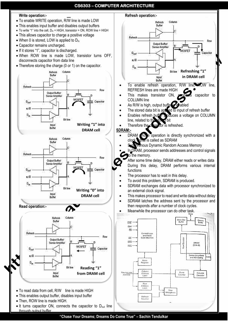
CS6303 – COMPUTER ARCHITECTURE
“Chase Your Dreams; Dreams Do Come True” – Sachin Tendulkar
Write operation:- __
To enable WRITE operation, R/W line is made LOW
This enables input buffer and disables output buffers To write “1” into the cell, Din = HIGH, transistor = ON, ROW line = HIGH
This allows capacitor to charge a positive voltage
When 0 is stored, LOW is applied to Din.
Capacitor remains uncharged.
If it stores “1”, capacitor is discharged.
When ROW line is made LOW, transistor turns OFF, disconnects capacitor from data line
Therefore storing the charge (0 or 1) on the capacitor.
Read operation:-
To read data from cell, R/W line is made HIGH
This enables output buffer, disables input buffer
Then, ROW line is made HIGH.
It turns capacitor ON, connects the capacitor to Dout line through output buffer
Refresh operation:-
To enable refresh operation, R/W line, ROW line,
REFRESH lines are made HIGH
This makes transistor ON, connects capacitor to COLUMN line
As R/W is high, output buffer is enabled
The stored data bit is applied to input of refresh buffer
Enables refresh buffer produces a voltage on COLUMN line, related to the stored bit
Therefore the capacitor is refreshed. SDRAM:-
DRAM whose operation is directly synchronized with a clock signal is called as SDRAM
Synchronous Dynamic Random Access Memory
In DRAM, processor sends addresses and control signals to the memory.
After some time delay, DRAM either reads or writes data
During this delay, DRAM performs various internal functions
The processor has to wait in this delay.
To avoid this problem, SDRAM is produced.
SDRAM exchanges data with processor synchronized to an external clock signal.
This makes processor to read and write data without delay
SDRAM latches the address sent by the processor and then responds after a number of clock cycles.
Meanwhile the processor can do other task.
Writing “1” into
DRAM cell
Writing “0” into
DRAM cell
Reading “1”
from DRAM cell
Refreshing “1”
in DRAM cell

CS6303 – COMPUTER ARCHITECTURE
“Chase Your Dreams; Dreams Do Come True” – Sachin Tendulkar
Timing Diagram of burst data transfer of length 4
DDR SDRAM:-
Fastest version of SDRAM
DDR Double Data Rate
SDRAM performs operations on rising edge of the clock signal
But DDR SDRAM performs operations on both the edges of clock signals
The bandwidth is doubled in DDR
It is also called as faster SDRAM
Two banks of cell arrays are there in DDR SDRAM
It is dual bank architecture
Each bank can be accessed separately
Nowadays, DDR version II and III is released
ROM:-
They can store the data even after power is OFF
We cannot write data to it
Non-volatile memory
It is used to store binary codes
It contains only Diode and decoder
Address lines A0 and A1 are decoded by 2 : 4 decoder
PROM:-
Programmable ROM
It has diodes in every bit position
Output is initially all 0s
Each diode has fusible series link.
By addressing the bits and applying proper current pulse at output, we can blow out that fuse, store “1” at that bit
Fuse is made up of nichrome
For blowing, pass 20 – 50 mA current for 5 – 20 µs
This blowing occurs according to truth table of PROM
PROM programmers can do it programmatically
That is why the name is called as PROM
They are one-time programmable, once programmed, information cannot be erased.
EPROM:-
Erasable PROM
They use MOS circuit
They store 0s and 1s as a packet of charge in IC.
They also can be programmed by EPROM programmers
We can erase the data in it, by exposing the chip to UV light through quartz window for 15 – 20 mins
We cannot erase selective information, all information will be vanished.
It can be re-programmed and re-used many times EEPROM:-
It also uses MOS circuit
Data is stored as: CHARGE or NO CHARGE
20 – 25 V charge is used to move charges
We can selectively erase information
They are expensive than ROM Flash memory:-
They are RW memories (both READ and WRITE)
We can read contents of a single cell, but can write whole block of cells
It is based on single transistor controlled by trapped charge
They have higher capacity, less power consumption
It is suitable for Laptop, tablets, smartphones, iPod, etc.
Types: Flash card (memory card) 1 GB to 64 GB Flash drive(pen drive) maximum 64GB capacity
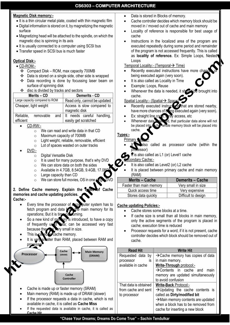
CS6303 – COMPUTER ARCHITECTURE
“Chase Your Dreams; Dreams Do Come True” – Sachin Tendulkar
Magnetic Disk memory:-
It is a thin circular metal plate, coated with thin magnetic film
Digital information is stored on it, by magnetizing the magnetic surface
Magnetizing head will be attached to the spindle, on which the magnetic disc is spinning in its axis
It is usually connected to a computer using SCSI bus
Transfer speed in SCSI bus is much faster
Optical Disk:-
CD-ROM:- Compact Disk – ROM, max capacity 700MB Data is stored on a single side, other side is wrapped Data recording is done by focussing laser beam on
surface of spinning disk disc is divided by tracks and sectors
Merits – CD Demerits - CD Large capacity compared to ROM Read only, cannot be updated
Cheaper, light weight Access is slow compared to magnetic disk
Reliable, removable and efficient
It needs careful handling, easily get scratched
CD-RW:- o We can read and write data in that CD o Maximum capacity of 700MB o Light weight, reliable, removable, efficient o Lot of spaces wasted on outer tracks
DVD:- o Digital Versatile Disk o It is used for many purpose, that’s why DVD o We can store data on both the sides o Available in 4.7GB, 8.54GB, 9.4GB, 17.08GB o Large capacity than CD o We can store full movies, OS in one single DVD
2. Define Cache memory. Explain the types of Cache memories and cache updating policies. Cache:-
Every time the processor of a computer system has to fetch program and data from the main memory for its operations; But it is time consuming.
So a new kind of memory is introduced, to have a copy of frequently used data; can be accessed very fast because they are very small in size.
This is called as cache memory.
It is very smaller than RAM, placed between RAM and processor
Cache is made up or faster memory (SRAM)
Main memory (RAM) is made up of DRAM (slower)
If the processor requests a data in cache, which is not available in cache, it is called as Cache Miss
If the requested data is available in cache, it is called as Cache Hit
Data is stored in Blocks of memory.
Cache controller decides which memory block should be moved in / moved out of cache and main memory
Locality of reference is responsible for best usage of cache
Instructions in the localized area of the program are executed repeatedly during some period and remainder of the program is not accessed frequently. This is called as locality of reference. Ex: Simple Loops, Nested Loops
Temporal Locality:- (Temporal Time)
Recently executed instructions have more chances of being executed again (very soon).
It is also called as Locality in Time
Example: Loops, Reuse
Whenever the data is needed, it should be brought into cache.
Spatial Locality:- (Spatial Space)
Recently executed instructions that are stored nearby, have more chances of being executed again (very soon).
Ex: straight line code, array access, etc Whenever data is needed, that particular data alone will not
be placed into cache, whole memory block will be placed into cache.
Types:- Primary Cache:-
It is also called as processor cache (within the processor)
It is also called as L1 (or) Level1 cache Secondary Cache:-
It is also called as Level2 (or) L2 cache
It is placed between primary cache and main memory (RAM)
Merits – Cache Demerits – Cache Faster than main memory Very small in size
Quick access time Very expensive
Stores data quickly Difficult to design
Cache updating Policies:-
Cache stores some blocks at a time.
If cache size is small than all blocks in main memory, only the active segments of the program is placed in cache; execution time is reduced
Processor requests for a word, if it is not present, cache controller decides which block should be removed out of cache.
Read Hit Write Hit
Requested data by processor is available in cache
Cache memory has copies of data in main memory. Write-Through protocol:- Contents in cache and main memory are updated simultaneously to avoid confusion
That data is obtained from cache and sent to processor
Write-Back Protocol:- Updating the cache contents is called as Dirty/modified bit Main memory contents are updated when a block has to be removed from cache for inserting a new block
Processor Cache (SRAM)
Main Memory (DRAM)
Cache Controller

CS6303 – COMPUTER ARCHITECTURE
“Chase Your Dreams; Dreams Do Come True” – Sachin Tendulkar
Read Miss Write Miss
Block of words that contains the requested word, is copied from main memory to cache
After entire block is loaded in cache, requested word is sent to processor. --If requested word doesn’t exists in cache during write operation, WRITE MISS will occur.
During READ, requested word is not in cache, there READ MISS will occur
If write-through protocol is used, data is directly written to main memory.
If write-Back protocol is used, blocks containing addressed word are first put in cache, then the required word in cache is overwritten with new data.
To overcome this, Load-Through/ Early restart protocol is used
3. Explain the techniques used to reduce the cache miss. (or)
Explain the methods of mapping functions and how are they useful in improving cache performance.
(or) Explain the mapping techniques in cache with neat diagram
Usually cache memory can store only limited number of blocks at a time. So, it can hold only a very small amount of blocks from main memory
This management of blocks between main memory and cache memory is called as mapping function.
There are two kinds of mapping techniques in cache organization:-
Before going into techniques, some assumptions are made:-
Cache consists of 128 blocks of 16 words each
Total cache size = 128 * 16 2048 (2K) words
1 page in main memory = group of 128 blocks of 16 words each
Main memory has 32 pages
128*16=2048 * 32 = 65536
Main memory has 65536 words Direct Mapping:-
Simplest mapping technique
Each block from main memory has one location in cache.
Block ‘I’ of main memory mapped to block i%128 of cache Main memory Blocks 0,128,256, …are stored in cache block 0
Main memory blocks 1, 129, 257, ..are stored in cache block 1
Here, address is divided into three fields: Tag,Block,Word
Word field: Select a word out of 16 words in cache
Block field: Contains 7 bits, because 128 blocks in cache(27=128)
Tag Field: Select a page among 32pages in main memory
Higher order 5 bits are compared with tag bits associated with that cache location
If they match, then required word is present in that cache block
If they does not match, the required block is not present in cache, so, read from main memory, load into cache
Merits – Direct Mapping Demerits – Direct Mapping
Easy to implement and understand
Processor needs to access same memory location from two different pages on main memory frequently
Less time consumed in implementing directly
But only one location will be present in cache at a time
Cache is directly mapped with main memory
Not flexible
Fully Associative Mapping:- Main block can be placed into any cache block position
Address contains only two fields: Word, Tag
Tag: To identify a memory block when it is in cache
Higher order 12 bits of an address received from CPU compared with tag bits of each cache block, to check whether required block is present or not.
If required block is present in cache, Word field is used to find required word from cache
We have freedom of choosing cache location for storing main memory block
If a new block enters cache, it has to remove the old blocks in cache only if the cache is full.
Here, for replacement of cache blocks, replacement algorithms are used (LRU, LFU, FIFO, Random).
Compare higher order bits of main memory address is compared with all 128 tags corresponding to each block, to check whether requested block is present in cache.
Merits – Direct Mapping Demerits – Direct Mapping
Place a main memory block anywhere in cache
Compare Tag bits with all 128 tags of cache for checking whether block is present in cache or not
Mapping
techniques
Direct
Mapping
Associative
Mapping
Fully
Associative
Set
Associative

CS6303 – COMPUTER ARCHITECTURE
“Chase Your Dreams; Dreams Do Come True” – Sachin Tendulkar
Two-way set associative mapping:-
Set associative = direct mapping + associative mapping
Many groups of direct mapped blocks operate as many direct mapped caches in parallel
A block of data from any page in main memory can go into particular block of directly mapped cache
Required address comparison depends on number of direct mapped caches in cache system
These comparisons are always less than the comparisons in fully associative mapping
Size of 1 page in main memory = size of 1 directly mapped cache
It is called as two way set associative because, each block from main memory has two choices for placing block.
Main memory Blocks 0, 64, 128, … can map into any 1 of cache blocks of set 0
Main memory blocks 1, 65, 129, … can map into any 1 of cache blocks of set 1, and so on
Three fields are needed
Word field: select one of 16 words in a block
Set field: find requested block from set 0 to set 64
Tag field: 6 bits, because, 64 pages are there ( 26) Merits – set-associative
Two directly mapped caches available;
Only two comparisons required to check given block is present of not
Reduced hardware cost
improved cache hit ratio
4. Explain the organization of virtual memory and its address translation technique with neat diagrams.
In modern computers, main memory is not enough for all the operations required by a processor of a computer
So, virtual memory (VM) technique is used to extend the size of main memory (RAM)
It uses secondary storage such as disks, pendrives, etc.
Virtual means imaginary. An imaginary memory is created inside the operating system, so that the user will get a feel that, main memory is this much large.
For example, if a 32GB movie has to be displayed, main memory is not enough to store it, so that 32GB movie is divided into segments.
Now, the currently running segment of the movie is played in main memory, remaining are stored in secondary storage.
If next segment of movie is needed, it replaces the previous segment in main memory
OS is responsible for management of VM
Here, the addresses issued by processor called as virtual address / logical address
They are converted into physical address (real address).
Similarly, many applications can be run on a computer at the same time, such as MS word, VLC, games, etc
There is not enough space in main memory to contain all these applications
But, in all these applications, only a small part will be currently active; so it is enough to load that part alone into RAM
This concept is called as VM

CS6303 – COMPUTER ARCHITECTURE
“Chase Your Dreams; Dreams Do Come True” – Sachin Tendulkar
Address Translation:-
address is broken into virtual page number and page offset
virtual page number is converted to physical page number
physical page number contains upper portion of physical address, page offset contains lower portion of address
number of bits in page offset decides the page size
page table is used to maintain information about main memory location of each page
The page is stored in which address of main memory, current status of page also stored in page table
To find address of corresponding entry in page table, Virtual page number + contents of page table base register
Page table base register has starting address of page table
The entry in page table gives physical page number
Add this physical page number + offset to get physical address in main memory
If required page is not present in main memory, PAGE FAULT occurs; that page is loaded from secondary storage to main memory by a program, PAGE FAULT ROUTINE
The technique of getting desired page in main memory is called as DEMAND PAGING
To support Demand Paging and VM, processor has to access page table in main memory
To avoid this access time, a part of page table is kept in main memory, called as TLB (Translation Lookaside Buffer)
Buffer means, a temporary storage place.
TLB stores part of page table entries (recently used pages)
Virtual address to physical address translation
Segment Translation:-
Every segment selector has a linear base address associated with it and stored in segment descriptor.
A Selector is used to point the descriptor for segment in a table of descriptions
Linear base address from descriptor is then added to the 32-bit offset to generate 32bit linear address
This process is called as SEGMENTATION or SEGMENT TRANSLATION
If paging unit is not enabled, then the 32bit linear address corresponds to the physical address.
If paging unit is enabled, paging mechanism translated linear address space into physical address space by paging process. Segment translation = Convert Logical address to Linear address
Page Translation:-
It is the second phase of address translation Segment translation translates logical address to linear address
Page translation converts that linear address to physical address When paging is enabled, the paging unit arranges the
physical address space into 1,048,496 pages of each 4096(4KB) long

CS6303 – COMPUTER ARCHITECTURE
“Chase Your Dreams; Dreams Do Come True” – Sachin Tendulkar
5. Explain the purpose and working of TLB with a diagram.
It is also called as Page Translation Cache
If processor refers two directories Page directory and page table, performance will be reduced. To solve this problem, the processor stores the most recently used page table entries in ON-CHIP cache. This is called as TLB
It can hold up to 32 page table entries.
32 page table entry coupled with 4K page size, results in coverage of 128K bytes of memory addresses
Page table is placed in main memory, but a copy of small portion of page table is placed in processor chip. This memory is called as TLB
Based on virtual address, MMU (Memory Management Unit) searches TLB for required page
If page table entry for that page is found in TLB, Physical address can be obtained immediately
IF entry not found, there is a Miss in TLB, The required entry is got from page table in RAM, and then stored in TLB
If OS makes any changes to any entry in the page table, control bit in TLB will invalidate that entry in TLB
When a program generates an access request to a page, that is not in main memory, page fault will occur.
That page should be brought from secondary storage (disk)
When it detects a page fault, MMU asks the OS to generate interrupt
OS will suspend the execution of the task which has created page fault, and starts execution of another task, whose pages are ready in main memory.
When the suspended task resumes, that instruction must be continued from the point of interruption, Or, that instruction must be restarted.
If a new page is brought from Disk, and main memory is full now, then that new page should replace a page from the main memory according to LRU algorithm (Least Recently Used)
Modified page is written to disk before removed from main memory.
Write through protocol is used for this task.
6. Explain the Programmed I/O data transfer technique.
I/O operation means, a data transfer between an I/O device
and memory (or) between an I/O device and the processor
In a computer system, if all the I/O operations are controlled by processor, then that system is using PROGRAMMED I/O
If that technique is used, processor executes programs that start, run and end the I/O operations including sensing device status, sending a R/W command or transferring data
Processor periodically checks status of I/O system until the operation is completed
Example:-
Processor’s software checks each of I/O devices regularly
During the check, microprocessor sees whether any device needs any service or not.
The following diagram services I/O ports A, B and C
The routine (program) checks the status of I/O ports
It first transfers status of I/O port A into accumulator
Then the routine checks contents of accumulator to check service request bit is SET or RESET
If SET, I/O port A service routine is called
After completing, it moves on to port B
The process is repeated again
It continues till all the I/O ports status registers are tested and all I/O ports are serviced.
Once this is done, processor continues to execute normal programs
When programmed I/O is used, processor fetches I/O related instructions from memory and gives the necessary I/O commands to I/O system for execution
Technique used for I/O addressing is followed (memory mapped I/O or I/O mapped I/O)
When processor sees an I/O instruction, the addressed I/O port is expected to be ready to respond, to avoid info loss.
Thus, a processor should know I/O device status always.
In Programmed I/O systems, processor is usually programmed to test the I/O device status before data transfer.

CS6303 – COMPUTER ARCHITECTURE
“Chase Your Dreams; Dreams Do Come True” – Sachin Tendulkar
7. What is DMA? Explain DMA cycles and configuration with neat diagrams.
It comes under hardware controlled data transfer
An external device is used to control the data transfer
External device generated the address and control signals to control the data transfer
It allows the peripheral device to directly access the memory
This technique is called as DIRECT MEMORY ACCESS
That external device that controls the data transfer is called as DMA CONTROLLER
DMA Idle Cycle:- When the system is turned ON, the switches are in ‘A’ position
The buses are connected from processor to system memory and peripherals
Processor executes the program until it needs to read a block of data from disk
To do this, processor sends series of commands to disk controller, telling it to search and read desired block of data
When disk controller is ready to transfer first byte of data from disk, it sends DMA request (DRQ), which is a signal to DMA controller.
Then DMA controller sends a hold request (HRQ), which is a signal to the processor to HOLD input
The processor responds to this HOLD signal by sending acknowledgement (HLDA) to DMA controller.
When DMA controller receives HLDA signal, it sends control signal to change switch position from A to B
This disconnects the processor from the buses and connects DMA controller to the buses
DMA Active Cycle:-
When DMA controller gets control of the buses, it sends memory address where first byte of data from the disk is to be written
It also sends DMA Acknowledge, DACK signal to disk controller device, telling it to get ready to send the byte
Finally it asserts IOR and MEMW signals on control bus
IOR (I/O Ready) signal enables disk controller to send byte of data from disk on data bus
MEMW (Memory Write) signal enables addresses memory to accept data from data bus
CPU is involved only at the beginning and at the end of data transfer operations.
Data transfer is monitored by DMA controller, which is also called as DMA channel
When CPU wants to read or write a block of data, it issues a command to the DMA module, with these instructions:- R/W operation Address of I/O device involved in this operation Starting address in memory to read or write No. of words to be Read/Written
DMA channel:-
It consists of Data counter, data register, address register, control logic
Data counter stores number of data transfers to be done in one DMA cycle
It is decremented automatically after each word transfer
Data register acts as a buffer
Address register stores starting address of device
When data counter is ZERO, DMA transfer is stopped
DMA controller sends an interrupt to processor saying that the DMA operation is finished.
Diagram (a) shows that the CPU, DMA module, I/O system and memory share the same system bus
Here Programmed I/O is used
Data transferred between memory and I/O system through DMA module
Each transfer of a word consumes two bus cycles
Diagram (b) shows that there is a different path between DMA module and IO system
This is another DMA configuration
Diagram I is third type of DMA configuration
Here I/O are connected to module using I/O bus
This reduces number of I/O interfaces in DMA module

CS6303 – COMPUTER ARCHITECTURE
“Chase Your Dreams; Dreams Do Come True” – Sachin Tendulkar
8. Explain the different data transfer modes in DMA. DMA controller transfers data in any one of the following modes: Single Transfer Mode (Cycle Stealing) Block Transfer Mode Demand (or) Burst Transfer Mode Single Transfer Mode:-
In this mode, device can make only one transfer (byte). After each transfer, DMAC gives control of all buses to
processor Series of operations
I/O device asserts DRQ line when it is ready to transfer data
DMAC asserts HLDA line to request use of the buses from processor
Processor asserts HLDA, granting bus control to DMAC
DMAC asserts DACK to request I/O device, executes DMA bus cycle and data transfer
I/O device deasserts its DRQ after data transfer of 1 Byte
DMA deasserts DACK line
Byte transfer count is decremented, memory address is incremented
HOLD line deasserted to give back control of all buses to processor
HOLD signal reasserted to request use of buses when I/O device ready to transfer another byte; same process repeated until last transfer
When data transfer count is ZERO, transfer is finished. Block Transfer Mode:-
Here, device can make number of transfers as programmed in the word count register.
After each transfer of word, count is decremented by 1, address is incremented by 1
DMA transfer is continued until word count becomes ZERO
It is used when DMAC needs to transfer a block of data Series of operations
I/O device asserts DRQ line when it is ready to transfer data
DMAC asserts HLDA line to request use of the buses from processor
Processor asserts HLDA, granting bus control to DMAC
DMAC asserts DACK to request I/O device, executes DMA bus cycle and data transfer
I/O device deasserts its DRQ after data transfer of 1 Byte
DMA deasserts DACK line Transfer count is decremented, memory address is incremented
When transfer count = ZERO, data transfer is not complete, DMAC waits for another DMA request from I/O
If transfer count is not ZERO, data transfer is finished, DMAC deasserts HOLD to tell processor , it does not need buses hereafter
Processor then deasserts HLDA signal to tell DMAC that it has got back control of the buses
Demand Transfer Mode:-
Here the device is programmed to continue data transfer until TC (Terminal Count) or EOP (End of Process) signal is encountered, or until DREQ (DMA Request) is inactive
Series of operations 1. I/O device asserts DRQ line when it is ready to transfer data
2. DMAC asserts HLDA line to request use of the buses from processor
3. Processor asserts HLDA, granting bus control to DMAC 4. DMAC asserts DACK to request I/O device, executes
DMA bus cycle and data transfer 5. I/O device deasserts its DRQ after data transfer of 1 Byte 6. DMA deasserts DACK line 7. Byte transfer count is decremented, memory address is
incremented 8. DMAC continues to execute data transfer until TC or EOP
is encountered 9. I/O device can restart DMA request by sending DRQ
(DMA Request) signal once again 10. Data transfer continues until transfer count = ZERO
Single Transfer Mode:-
Block Transfer Mode:-

CS6303 – COMPUTER ARCHITECTURE
“Chase Your Dreams; Dreams Do Come True” – Sachin Tendulkar
Demand Transfer Mode:-
9. Explain in detail the Bus Arbitration techniques in DMA
The device that is allowed to initiate data transfer on bus at any given time is called as BUS MASTER
In a computer system, there may be more than one bus master such as processor, DMA controller, etc
They share system bus
When current Bus Master gives back bus control, another bus master gets the bus control.
Bus arbitration is defined as the process by which the next device to become bus master is selected and bus mastership is transferred to it.
Selection is done on priority basis
There are two types of bus arbitration techniques in DMA;-
Centralized arbitration technique Distributed arbitration technique
Centralized arbitration Technique:-
A single bus arbiter performs the arbitration
The bus arbiter may be processor or a separate controller
Three types of centralized arbitration. They are:- Daisy chaining Polling Method Independent Request
Daisy Chaining:-
It is a simpler and easy method
All masters make use of same line for bus request
In response to a bus request, controller sends a BUS GRANT signal if bus is free
BUS GRANT signal serially propagates through each master until it encounters first one that is requesting access to bus
This master blocks the propagation of the BUS GRANT signal, activates BUSY LINE signal and gains control of bus
Any other requesting module will not receive grant signal and cannot get bus access
Adv-Daisy Chaining Disadv-Daisy Chaining
Simpler and cheaper method Propagation delay of bus grant signal is proportional to number of masters in the system. This makes arbitration time slow, therefore limited number of masters are allowed in a system
It requires the least number of lines and independent of number of masters in the system
Priority of master is fixed by its physical location
Failure of one master makes whole system failure
Polling Method:-
Controller is used to generate addresses for masters
Number of address lines required depends on number of masters connected in the system
If there are 8 masters in the system, at least three address lines needed
If anybody sends BUS request, controller generates a sequence of master addresses
When requesting, master finds its address, activates BUSY line signal.
Adv-Polling method
Priority can be changed by changing polling sequence in the controller
If one module fails, entire system does not fail
More improved than the daisy chaining method.

CS6303 – COMPUTER ARCHITECTURE
“Chase Your Dreams; Dreams Do Come True” – Sachin Tendulkar
Independent priority method:-
Each master has a separate pair of bus request and BUS GRANT lines and each pair has a priority assigned to it
The built-in priority decoder within the controller selects highest priority request and asserts corresponding BUS GRANT signal.
Adv-Independent priority
Due to the separate pair of bus request and bus grant signals, arbitration is fast Arbitration is independent of number of masters in the system
Disadv-Independent Priority
It requires more bus request and bus grant signals
Distributed arbitration:-
All devices participate in selection of next bus master
Each device on bus is assigned a 4bit ID
The number of bits in ID depends on number of devices
When one or more devices request for bus control, they assert START-ARBITRATION signal and place their 4bit ID on arbitration lines, ARB0 to ARB3
More than one device can place their 4bit ID to indicate that they need control of bus
If one device puts 1 on bus line, another device puts 0 on same bus line, bus line status will be 0
Device reads status of all lines through inverter buffers, so device reads bus status 0 as logic 1
Device having highest ID, has highest priority
When two or more devices place their ID on bus lines, it is necessary to find highest ID from status of bus line
For example, consider two devices A and B having ID 1 and 6, request for bus
Device A puts bit pattern 0001, device B puts 0110
With this combination, the bus line status will be 1000
Inverter buffers code seen by both devices is 0111
Each device compares code formed on arbitration lines to its own ID, starting from MSB
If it finds a difference at any bit position, it disables drives at that position by placing 0 at input of all these drives
Here, device detects a difference on line ARB2
It disables drives on lines ARB2, ARB1, ARB0
This makes code on arbitration lines to change to 0110
0110 6, which is ID of B
This means, B wins the competition
Adv:-
It offers high reliability because operation of bus is not dependent on any single device.
10.What are Interrupts? Explain the Interrupt hardware in detail with necessary diagrams. Interrupts:-
An External event that affects the normal flow of instruction execution generated by the external hardware devices such as keyboard, mouse, etc is called as interrupts
Ex: computer should response to keyboard, mouse, etc when they ask something.
If a device wants to tell processor about the completion of an operation, it sends a hardware signal,, that signal is called as Interrupt
A special Routine that is executed to give service to the interrupts is called as Interrupt Service Routine (ISR)
Interrupt request line is used to alert the processor
A program can be interrupted in three ways:- By external signal By a special instruction in the program By some other condition
Ex:- Main program Instruction1:______ ; INTERRUPT OCCURS HERE ; Instruction n:_______
ISR . . . .

CS6303 – COMPUTER ARCHITECTURE
“Chase Your Dreams; Dreams Do Come True” – Sachin Tendulkar
An interrupt is caused by an external signal is called as hardware interrupt
Conditional interrupts (or) interrupts is created by special instructions are called as software interrupts
Interrupt Hardware:-
An I/O device requests an interrupt by activating a bus line called as interrupt request (or) request
Interrupts are classified as Single level and Multilevel interrupt Single level Interrupts:-
There can be many interrupting devices. But all interrupt
requests are made via a single input pin of CPU
When interrupted, CPU has to poll the I/O ports to identify requested device
Polling software routine that checks the state of each device.
Once the interrupting I/O port is found, CPU will service it and then return to task it was performing before the interrupt
Interrupt request from all devices are logically ORed and connected tointerrupt input of processor
The interrupt request from any device is routed to processor interrupt input
After getting interrupted, processor identifies requesting device by reading interrupt status of each device
All devices connected to INTR line via ground switches
To request an interrupt, device closes its associated switch
Interrupt signals I0 ….. In, interrupt request line will be equal to VDD
When a device requests for reply, voltage line drops to zero
If a signal is closed, Flag 0 is used; INTR=1
Open collector and open drain gates are used
Because o/p of open collector (or) an open drain gate is equivalent to a switch to ground that is open\
Multi-Level interrupts:-
Processor has more than one interrupt pins
I/O devices are tied to individual interrupt pins
They can be immediately classified by CPU upon receiving an interrupt request from it
This allows processor to go directly to that I/O device and service it without polling concept
This saves time in time processing input
When a process interrupted, it stops executing its current program, and calls special routine
The event causes interruption is called as interrupt
Processor finishes its current instruction; no cut-off
Program counter’s current details stored in stack
Remember during pgrm execution of an instruction PC is loaded with address of ISR
Interrupt programs continue working until result executed
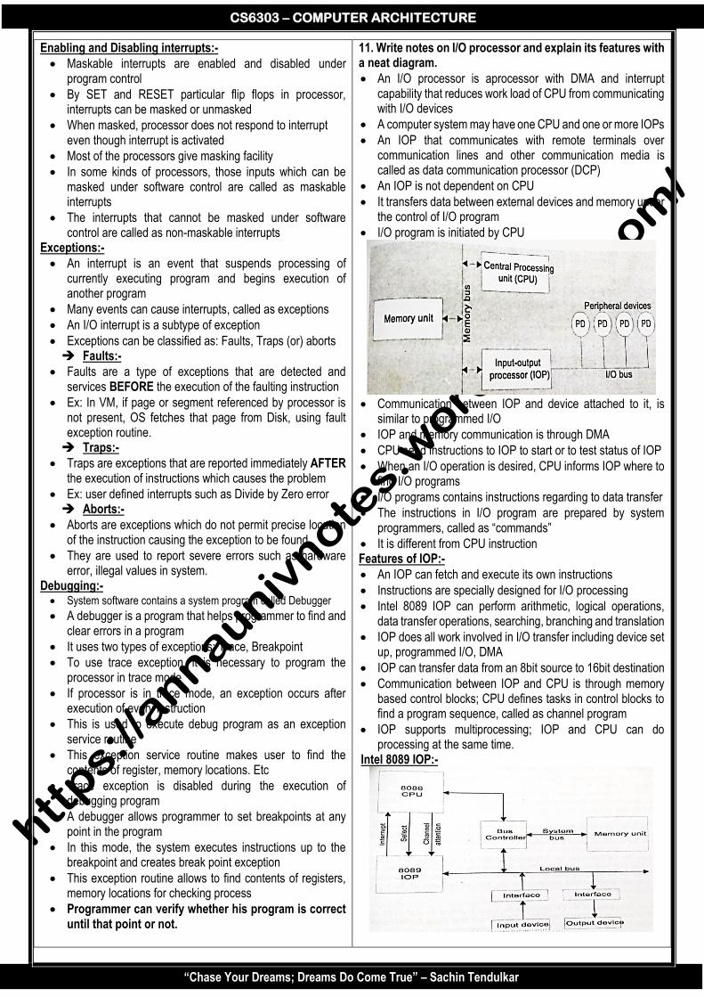
CS6303 – COMPUTER ARCHITECTURE
“Chase Your Dreams; Dreams Do Come True” – Sachin Tendulkar
Enabling and Disabling interrupts:-
Maskable interrupts are enabled and disabled under program control
By SET and RESET particular flip flops in processor, interrupts can be masked or unmasked
When masked, processor does not respond to interrupt even though interrupt is activated
Most of the processors give masking facility
In some kinds of processors, those inputs which can be masked under software control are called as maskable interrupts
The interrupts that cannot be masked under software control are called as non-maskable interrupts
Exceptions:-
An interrupt is an event that suspends processing of currently executing program and begins execution of another program
Many events can cause interrupts, called as exceptions
An I/O interrupt is a subtype of exception
Exceptions can be classified as: Faults, Traps (or) aborts Faults:-
Faults are a type of exceptions that are detected and services BEFORE the execution of the faulting instruction
Ex: In VM, if page or segment referenced by processor is not present, OS fetches that page from Disk, using fault exception routine. Traps:-
Traps are exceptions that are reported immediately AFTER the execution of instructions which causes the problem
Ex: user defined interrupts such as Divide by Zero error Aborts:-
Aborts are exceptions which do not permit precise location of the instruction causing the exception to be found
They are used to report severe errors such as hardware error, illegal values in system.
Debugging:- System software contains a system program called Debugger
A debugger is a program that helps programmer to find and clear errors in a program
It uses two types of exceptions: Trace, Breakpoint
To use trace exception, it is necessary to program the processor in trace mode
If processor is in trace mode, an exception occurs after execution of every instruction
This is used to execute debug program as an exception service routine
This exception service routine makes user to find the contents of register, memory locations. Etc
Trace exception is disabled during the execution of debugging program
A debugger allows programmer to set breakpoints at any point in the program
In this mode, the system executes instructions up to the breakpoint and creates break point exception
This exception routine allows to find contents of registers, memory locations for checking process
Programmer can verify whether his program is correct until that point or not.
11. Write notes on I/O processor and explain its features with a neat diagram.
An I/O processor is aprocessor with DMA and interrupt capability that reduces work load of CPU from communicating with I/O devices
A computer system may have one CPU and one or more IOPs
An IOP that communicates with remote terminals over communication lines and other communication media is called as data communication processor (DCP)
An IOP is not dependent on CPU
It transfers data between external devices and memory under the control of I/O program
I/O program is initiated by CPU
Communication between IOP and device attached to it, is
similar to programmed I/O
IOP and memory communication is through DMA
CPU send instructions to IOP to start or to test status of IOP
When an I/O operation is desired, CPU informs IOP where to find I/O programs
I/O programs contains instructions regarding to data transfer
The instructions in I/O program are prepared by system programmers, called as “commands”
It is different from CPU instruction Features of IOP:-
An IOP can fetch and execute its own instructions
Instructions are specially designed for I/O processing
Intel 8089 IOP can perform arithmetic, logical operations, data transfer operations, searching, branching and translation
IOP does all work involved in I/O transfer including device set up, programmed I/O, DMA
IOP can transfer data from an 8bit source to 16bit destination
Communication between IOP and CPU is through memory based control blocks; CPU defines tasks in control blocks to find a program sequence, called as channel program
IOP supports multiprocessing; IOP and CPU can do processing at the same time.
Intel 8089 IOP:-