studies on the electrical transport properties of carbon
TRANSCRIPT

Louisiana Tech UniversityLouisiana Tech Digital Commons
Doctoral Dissertations Graduate School
Summer 2016
Studies on the electrical transport properties ofcarbon nanotube compositesTaylor Warren Tarlton
Follow this and additional works at: https://digitalcommons.latech.edu/dissertations
Part of the Materials Science and Engineering Commons, and the Nanoscience andNanotechnology Commons

STUDIES ON THE ELECTRICAL TRANSPORT
PROPERTIES OF CARBON NANOTUBE
COMPOSITES
by
Taylor Warren Tarlton, M.S. Applied Physics, B.S. Physics
A Dissertation Presented in Partial Fulfillment of the Requirements for the Degree
Doctor of Philosophy in Engineering: Engineering Physics
COLLEGE OF ENGINEERING AND SCIENCE LOUISIANA TECH UNIVERSITY
August 2016

ProQuest Number: 10307867
All rights reserved
INFORMATION TO ALL USERS The quality of this reproduction is dependent upon the quality of the copy submitted.
In the unlikely event that the author did not send a complete manuscript and there are missing pages, these will be noted. Also, if material had to be removed,
a note will indicate the deletion.
ProQuest 10307867
ProQuestQue
Published by ProQuest LLC(2017). Copyright of the Dissertation is held by the Author.
All rights reserved.This work is protected against unauthorized copying under Title 17, United States Code.
Microform Edition © ProQuest LLC.
ProQuest LLC 789 East Eisenhower Parkway
P.O. Box 1346 Ann Arbor, Ml 48106-1346

LOUISIANA TECH UNIVERSITY
THE GRADUATE SCHOOL
June 20th, 2016
Date
We hereby recommend that the dissertation prepared under our supervision
b Taylor Warren Tarlton
entitled_________________________________________________________________________________________________
Studies on the Electrical Transport Properties of Carbon Nanotube Composites
be accepted in partial fulfillm ent o f the requirements for the Degree o f
Ph.D. Engineering-Engineering Physics
.’isor o fD isscrta tio n Research
Head ol'Departm ent
R ecommendation cpnfurred in
/ ' P' -J ^ f p
Approved:
D irector o f Graduate Studies
XtsKjr, XteJ) / f c >Dean ol the C o llege /
PhysicsDepartment
Advisory Committee
Approved:
can o f the Graouate Schoo
C IS F o rm 13a (6/07)

ABSTRACT
This work presents a probabilistic approach to model the electrical transport
properties o f carbon nanotube composite materials. A pseudo-random generation method
is presented with the ability to generate 3-D samples with a variety of different
configurations. Periodic boundary conditions are employed in the directions
perpendicular to transport to minimize edge effects. Simulations produce values for drift
velocity, carrier mobility, and conductivity in samples that account for geometrical
features resembling those found in the lab. All results show an excellent agreement to the
well-known power law characteristic of percolation processes, which is used to compare
across simulations. The effect of sample morphology, like nanotube waviness and aspect
ratio, and agglomeration on charge transport within CNT composites is evaluated within
this model. This study determines the optimum simulation box-sizes that lead to
minimize size-effects without rendering the simulation unaffordable. In addition, physical
parameters within the model are characterized, involving various density functional
theory calculations within Atomistix Toolkit. Finite element calculations have been
performed to solve Maxwell’s Equations for static fields in the COMSOL Multiphysics
software package in order to better understand the behavior of the electric field within the
composite material to further improve the model within this work. The types of
composites studied within this work are often studied for use in electromagnetic
shielding, electrostatic reduction, or even monitoring structural changes due to

compression, stretching, or damage through their effect on the conductivity. However,
experimental works have shown that based on various processing techniques the
electrical properties of specific composites can vary widely. Therefore, the goal of this
work has been to form a model with the ability to accurately predict the conductive
properties as a function physical characteristics o f the composite material in order to aid
in the design of these composites.

APPROVAL FOR SCHOLARLY DISSEMINATION
The author grants to the Prescott Memorial Library o f Louisiana Tech University the right to reproduce,
by appropriate methods, upon request, any or all portions o f this Thesis. It is understood that “proper request”
consists o f the agreement, on the part o f the requesting party, that said reproduction is for his personal use and
that subsequent reproduction will not occur without written approval o f the author o f this Thesis. Further, any
portions o f the Thesis used in books, papers, and other works must be appropriately referenced to this Thesis.
Finally, the author o f this Thesis reserves the right to publish freely, in the literature, at any time, any
or all portions o f this Thesis.
Author
Date Jo.L !!■' 201 to
OS Form 14 (5/03)

DEDICATION
This work is dedicated first to my Lord Jesus Christ for his many blessings
and secondly to my beautiful wife fo r her steadfast love and encouragement
throughout this process. I would also like to thank my wonderful parents fo r
how they have raised me to always strive to be my best at whatever I pursue
in this life.
Taylor Warren Tarlton

TABLE OF CONTENTS
ABSTRACT.................................................................................................................................... i
DEDICATION............................................................................................................................. iii
LIST OF TABLES.......................................................................................................................vi
LIST OF FIGURES................................................................................................................... vii
ACKNOWLEDGMENTS........................................................................................................ xii
INTRODUCTION.........................................................................................................................11.1 Background.................................................................................................................11.2 About This W ork.......................................................................................................9
GENERAL METHODOLOGY.................................................................................................112.1 Generation of Virtual Nanocomposite Sam ples.................................................. 122.2 Finding nearest Neighbor Nanotubes.................................................................... 142.3 Nanotube Length Distributions.............................................................................. 192.4 Hopping Transport Algorithm...............................................................................20
EFFECTS OF MORPHOLOGY ON CONDUCTIVITY.....................................................273.1 Nanotube Waviness and Aspect Ratio..................................................................273.2 Agglomeration.........................................................................................................323.3 Sample Size.............................................................................................................. 433.4 Comparison to Experimental Data with Preexisting Routines..........................52
CHARACTERIZING THE HOPPING ALGORITHM........................................................554.1 Determining Tunneling Parameters......................................................................554.2 Charge Transport through Junctions..................................................................... 614.3 Charge Transport through CNTs........................................................................... 654.4 Improvements in the Transport Algorithm..........................................................68
EFFECTS OF THE LOCAL AND APPLIED ELECTRIC FIELDS.................................. 735.1 COMSOL Studies on Local Fields....................................................................... 745.2 Comparison to Experiments with the Improved Transport Routine.................945.3 Effect o f the Applied Electric Field on Conductivity.........................................96
CONCLUSIONS........................................................................................................................99
iv
RELATED AND FUTURE WORKS.....................................................................................1027.1 Further Improving this Model.............................................................................. 1027.2 Voids or Non-Conductive Inserts........................................................................1037.3 Further Characterization of Various Composites..............................................1057.4 Effects of Structural Changes on Charge Transport......................................... 107
7.4.1 Cracks in Samples................................................................................. 1077.4.2 Effect of Compression on Charge Transport..................................... I l l7.4.3 Vibrational Studies with Charge Transport.......................................1147.5 Polymer Hydrogel Simulations.............................................................117
BIBLIOGRAPHY..................................................................................................................... 116
v

LIST OF TABLES
Table 3.1. Fitting parameters for the power law for varying waviness in NT composites..............................................................................................................................30
Table 3.2. Parameters for the power law fits as a function o f aspect ra tio ...................31
Table 3.3. Power Law fitting parameters for varying sample lengths.......................... 45
Table 4.1. Tunneling constants, a, for various voltages in the rotated and bridgedconfigurations................................................................................................... 61
VI

LIST OF FIGURES
Figure 2.1.
Figure 2.2.
Figure 2.3.
Figure 2.4.
Figure 3.1.
Figure 3.2.
Figure 3.3.
Figure 3.4.
Figure 3.5.
Figure 3.6.
Schematic representation of the NT’s growth process segment-by-segment. In the simulation, the boxes are considered completely occupied by the NT segment...............................................................................................................13
Schematic representation of overlapping partitions for neighbor finding routine.................................................................................................................16
CPU wall times for calculating neighbor NTs for a specific sample with over 5000 NTs....................................................................................................18
NT length distribution (number of segments) presented as a percentage of NTs in the composite with a particular number o f segments (a) for a sample with NTs of uniform length (b) For a sample with NT’s length with aGaussian distribution. In b) the different percentage cases areindistinguishable from each other...................................................................20
Waviness Factor equal to a) 0.31, b) 0.5, c) 0.67, and d) 0 .71 .................. 28
Mobility vs NT concentration as a function of waviness. The two greyed data points are below the percolation threshold. However, they represent the cases in which very few charges reached the opposite electrode (0.49% for WF=0.31 0.46% for WF=0.5) so the statistics on these points is very poor 28
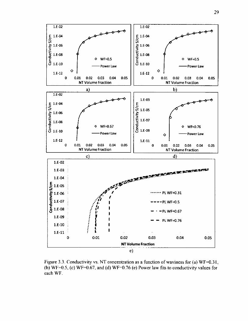
Conductivity vs. NT concentration as a function of waviness for (a) WF=0.31, (b) WF=0.5, (c) WF=0.67, and (d) WF=0.76 (e) Power law fits to conductivity values for each W F ............................................................... 29
Conductivity for varying aspect ratios of 1:1:50 and 1:75 with the associated power law fittings.............................................................................................31
A visual representation of a fully agglomerated sample..............................33
Method 1 samples with 12 initial seed NTs are shown with periodic representation at concentrations of d) 0.01, e) 0.02, and f) 0.03. Method 2 samples with 5% of the required volume of NTs being dispersed randomly in volume concentrations of g) 0.01, h) 0.02, i) 0.03. Method 3 samples with each new NT having a 5% probability for uniform dispersion are shown
vii

with periodic representation at concentrations of a) 0.01, b) 0.02, and c) 0.03. In these plots a periodic image above and below the central volume is shown................................................................................................................. 35
Figure 3.7.
Figure 3.8.
Figure 3.9.
Figure 3.10.
Figure 3.11
Figure 3.12
Figure 3.13
Figure 3.14
Figure 3.15
Figure 3.16
Figure 3.17
Figure 3.18
Figure 3.19
Normalized values for the charges reaching the collection electrode and mobility of those charges for concentrations of a) 0.01, b) 0.02, c) 0.03, and d) 0.04 when using method 1.......................................................................... 37
Normalized values for the charges reaching the collection electrode and mobility of those charges for concentrations of a) 0.01, b) 0.02, c) 0.03, and d) 0.04 when using method 2 .......................................................................... 38
Normalized values for the charges reaching the collection electrode and mobility of those charges for concentrations of a) 0.01, b) 0.02, c) 0.03, and d) 0.04 when using method 3 .......................................................................... 38
Conductivity vs a) UI-1, b) UI-2, and c) UI-3 for four volume concentrations................................................................................................... 40
a) A sample at a NT concentration of 0.02 and initialized with 12 seed NTs.b) Each NT highlighted with a color that represents the number of visits each NT received, c) Zoomed in view of the highly visited NTs within anagglomerate........................................................................................................43
Visuals for samples of different lengths........................................................44
Power law fit to conductivity for different box lengths...............................45
Samples with 5 nm length tubes at 0.005 volume fraction with lengths of a) 10 nm, b) 20 nm, c) 30 nm, d) 40 nm, and e) 50 n m ................................... 47
Simulation results for changing the maximum box length while keeping the NT size constant................................................................................................48
Various samples at a volume concentration of 0.015 for samples with maximum NT lengths of lOnm and sample lengths of a) 20 nm, b) 30 nm,c) 40 nm, d) 50 nm, e) 60 nm........................................................................ 49
Conductivity results for changing box length with NTs having constant length o f 10 nm ................................................................................................. 50
Samples with lengths of a) 250 nm, b) 300 nm, c) 400 nm, d) 600 nm, e) 800 nm, f) 1000 nm...........................................................................................51
Conductivity results for changing box length with NTs having constant length of 200nm................................................................................................ 52

Figure 3.20
Figure 4.1
Figure 4.2
Figure 4.3
Figure 4.4
Figure 4.5
Figure 4.6
Figure 4.7
Figure 4.8
Figure 4.9
Figure 5.1
Figure 5.2
Figure 5.3
Figure 5.4
Figure 5.5
Power law curves from simulation data fit to experimental data from works by Guo et al.[ 131] and Pradhan et al.[ 119].................................................. 53
Optimized CP2 molecule within Gaussian 0 9 '............................................. 57
Single monomer of CP2 Polyimide between two metallic CNTs 58
Two different views of the device with two (a and b) and three (c and d) separate monomers of CP2 polyimide in between two metallic CNTs connected to electrodes.................................................................................... 59
a) 1 and b) 2 monomers stretched end to end bridging the gap between the two metallic CNTs............................................................................................60
The current-distance relationship for the rotated configurations and the bridged configurations at the various distances............................................60
Two armchair CNTs distanced approximately 3 A apart to calculate the contact resistance between two metallic C N Ts............................................63
Current versus voltage for the device with two armchair C N T s............... 64
A single (5, 5) armchair CNT bridging two electrodes to measure the resistance o f a CNT.......................................................................................... 66
Current-Voltage relationship for a single CNT bridging two electrodes.. 67
a) Simulated COMSOL environment where NTs were approximated as rectangular prisms, b) Representation of cylindrical tube as rectangular prism, where the length of the diagonal on the rectangular face is equal to the diameter of the N T ..................................................................................... 77
The finite element mesh of a replicated sample in Comsol. The denser areas, or where there are more finite element grid locations, are located around the metallic inclusions............................................................................................78
Distributions for the x component of the local electric fields at volume concentrations of a) 0.01, b) 0.02, c) 0.03, and d) 0 .04 ...............................80
Focused distributions for the x component of the local electric fields at volume concentrations of a) 0.01, b) 0.02, c) 0.03, and d) 0 .04 .................81
The locations (red stars) in the 0.04 volume concentration sample where the x component of the electric field was greater than 10E0. The metallic inclusions are represented by the blue lines.................................................. 81
ix

Figure 5.7
Figure 5.8
Figure 5.9
Figure 5.10
Figure 5.11
Figure 5.12
Figure 5.13
Figure 5.14
Figure 5.15
Figure 5.16
Figure 5.17
Figure 5.18
Figure 5.19
The x component o f the electric field in the junction between neighbor NTs vs. the junction distance in samples with straight NTs at volume concentrations of a) 1%, b) 2%, c) 3%, and d) 4%. The applied electric field, E0 was 1000 V/m..............................................................................................82
Simple representation of how one of the shortest distances can arise in the sam ple................................................................................................................ 83
Visual representation o f how the junction distance of 3.66 can arise within samples. The two solid blue dots represent the two endpoints of two neighboring NTs. Each endpoint is capped with a semi-sphere. The two endpoints would exist in the cubic lattice as diagonal to each other 84
The distributions o f the x component of the local electric fields between junctions at the four shortest possible distances between NTs. The specified junction distances are in A ...............................................................................85
A a) Gaussian and b) Weibull distribution fit to the distribution of local fields in the junctions between neighboring N T s .........................................86
The distribution of values for the x component of the local electric fields within each junction classified for the charge transport routine................. 88
Conductivity results for varying the electric fields within samples using version 2 o f the transport routine....................................................................89
The distribution of the average values of the a) y component and b) z component of the fields within the junctions between neighboring NTs . 90
The norm of the electric field at the midpoint in each junction versus the junction distances for concentrations of a) 0.01, b) 0.02, c) 0.03, and d) 0.04 ............................................................................................................................. 91
The distributions of the local electric field norm between junctions at the four shortest possible distances between NTs...............................................92
Weibull fit to the combined distributions o f the local electric field norms for the 4 shortest junction distances in the 0.04 volume concentration case.. 93
The Weibull distributions for the x component and norm of the electric field in the midpoints of the junctions for the four shortest distances in the 0.04 concentration sam ple....................................................................................... 94
Comparison to experimental results from Guo et al. [ 131 ] and Pradhan et al.[ 119]with results under an applied electric field of 10 V /cm .................95
x
Figure 5.20
Figure 7.1
Figure 7.2
Figure 7.3
Figure 7.4
Figure 7.5
Figure 7.6
Figure 7.7
Figure 7.8
Figure 7.9
Conductivity results for varying the applied electric field.......................... 97
Samples with a second type of insert, shown here as voids, for volume concentrations of a) 0.00 and b) 0.05. The volume concentration o f the normal NTs (in green) was kept constant....................................................105
A simple crack forming through the middle of a virtual nanocomposite sam ple...............................................................................................................108
The number of charges, out of 1000, that reach the opposite electrode at each cracking step......................................................................................... 108
The path taken by one charge, highlighting the visited N T s.................... 109
a) The thinner crack from the 6% volume NT sample and b) The wider crack in the 8% volume NT sample.......................................................................110
The number of charges that reach the opposite electrode for the 6% volume sample (with a thinner crack) and 8% volume sample (with the thicker crack)...............................................................................................................111
Compression of samples towards the center of the sample Increasing compression from left to right......................................................................112
Percentage of charges reaching the collection electrode as the sample is compressed.....................................................................................................112
Hydrogel sample. The green segments are the polymer strands, and the redspots are the drug molecules in the sample................................................116
XI

ACKNOWLEDGMENTS
The author of this work would like to acknowledge the main research supervisor
for this work, Dr. Pedro Derosa, for his guidance throughout this process.
In addition, the advisory committee members, Dr. Lee Sawyer, Dr. Dentcho
Genov, Dr. Neven Simicevic, and Dr. Tom Bishop, are also thanked for their guidance
and advice on this project.
The Louisiana Board of Regents and Louisiana Tech University are also
acknowledged for their funding support for the author o f this work.
Valuable computational resources have been used from the Louisiana Optical
Network Initiative (LONI) supercomputing systems.
This project has been funded through the Air Force Research Labs.
XII

CHAPTER 1
INTRODUCTION
1.1 Background
Carbon Nanotubes (CNTs) were first discovered and described in 1991 by Sumio
Iijima of the NEC Corporation, Fundamentals Research Laboratories in Japan. The
discovery came by happenstance through an attempt to create C6o molecules through arc
discharge evaporation^ 1] Since then, CNTs have been intensively studied as they are of
interest for a number o f technological applications due to their exceptional electrical,
mechanical, and thermal properties.[2]-[8] CNTs can be blended into other materials to
improve certain characteristics of those materials. When these nanocomposite materials
are created, the overall composite can acquire some of the quality characteristics inherent
in CNTs, improving thermal properties, electrical conductivity, and/or mechanical
characteristics depending on the specific application.
CNTs can be either metallic or semiconducting based on the chirality o f the CNT,
which is essentially a quantification how a sheet o f graphene (hexagonally arranged
carbon atoms) could be rolled to obtain the specific CNT. CNTs can consist of one rolled
sheet in single-walled CNTs (SWCNT), or many concentric sheets in multi-walled CNTs
(MWCNT). The chiral vector, (m,n), determines how the sheet of graphene would be
rolled to form a CNT and is defined based on the unit vectors the hexagonal lattice. It has
been found that when m is equal to n, or m—n is a multiple of 3, the CNT will have a

2
minimized gap between the valence and conduction bands and behave as a metal.
Otherwise, the arrangement of carbon atoms induces a larger gap, causing the CNT to
become semi-metallic in nature. CNTs are comprised of conjugated carbon atoms, which
allow electrons to disassociate from specific atoms and occupy delocalized electronic
states. The semiconducting or metallic nature of each CNT then determines the
availability of those delocalized electronic states. In addition, the lengths of CNTs are on
the order o f the mean free path of electrons, leading to ballistic charge transport along the
axial direction o f the CNT.[2], [5], [7] Conductivity values of single CNTs have been
reported to be on the order of 105 S/m to 106 S/m.[9], [10]
Thermal conductivity of CNTs is exceptional along its axial direction due to the
ability of phonons to move along that direction. Values up to 6000 W/mK for thermal
conductivity has been reported in the literature for CNTs. However, many factors such as
atom arrangement, chirality, diameter, and surface defects play an important role in
determining thermal conductivity of individual nanotubes (NTs).[4], [8]
CNTs also have quality mechanical properties along the axial direction of the NT,
lending them exceptional tension strength. The Young’s Modulus of CNTs has been
measured to be 1 - 5 TPa along the axial direction. [11] They also possess a high degree
of flexibility, with the critical bending angle for SWCNTs being measured around
110°.[12]
CNTs have been widely studied for various purposes in order to take advantage of
their exceptional electrical, mechanical, and thermal properties. Numerous studies have
sought to use them as components in transistors as the semiconducting material
separating the source and drain components in attempts to further scale down the size of
3
modern field effect transistors (FETs).[13]-[16] Some studies have been quite successful
and have even led to small scale computers consisting of only CNT-FETs.[17] Much of
the work involving CNTs has focused on how the inclusion of CNTs into various
polymers[18]-[34], ceramics[35], [36], and epoxies[37]-[41] can produce enhancements
in electrical properties while also often times improving upon the mechanical and thermal
properties o f the original material. In these studies, CNTs are used as conductive fillers in
a specific type of matrix, and then the electrical properties o f the overall composite are
characterized versus the volume or weight fraction of CNTs. These conductive
composites can make matrix materials that are insulating without the CNTs useful for a
wide array of applications ranging from electromagnetic interference shielding[42]-[46],
electrostatic reduction[21], and strain sensing for structural health monitoring[39], [47]—
[51].
Many of the experimental studies on CNT composite materials cite the
importance of proper CNT dispersion for the qualities of the CNTs to be fully exhibited
through the composite materials. CNTs interact with other CNTs via Van-der-Waals
interactions, and therefore tend to coagulate, or agglomerate.[35] These bundles can, and
in early studies did, degrade the electrical conductivity in these composite materials.
Many studies have gone through repeated steps of sonication of samples[8], [ 19]—[21 ],
[23], [27]—[30], [34], [38]—[40], [48], [49], [52]-[72], functionalization of CNTs[35],
[52], [56], [73]—[76], shear mixing[23], [48], [49], [56], [58], [77]-[79], and other
processing methods in order to better disperse CNTs throughout the host matrix
materials.
4
The main reason quality dispersion is desired for various electrical applications is
that CNT composites consisting of electrically conductive CNTs and an insulating matrix
generally behave in close agreement with percolation theory.[41], [66], [80]—[83] At a
critical CNT concentration (percolation threshold), conductive networks begin to form
throughout the host matrix, allowing charge transport through the previously non-
conductive material and increasing the overall conductivity by several orders of
magnitude. Better dispersion of CNTs can enable more conduction pathways to form
throughout the composite material, allowing for either heat or charge transport to occur.
Materials previously not useful for electronic applications have exhibited conductivities
ranging from 10'7 - 10 S/m when mixed with CNTs, an increase of around 10 orders of
magnitude is some cases when compared to the bare matrix.[18], [37], [84]—[88]
A percolating material will typically follow the well-known power-law given by
Eq. (1.1).
(0 0 < 0r° ~ { o c (0 - 0 c ) f 0 > 0 c
Here, 0 is the filler concentration, 0 C is the critical concentration at which percolation
occurs, ac is the conductivity o f the nanoinsert, and / is the critical exponent. Given a
particular system, its conductivity curve can be fit to Eq. (1.1) with <rc, <pc, and t to be
used as fitting parameters.[81], [82] The value of t found from various experimental
works ranges between 1 and 6, with the majority of the values being less than 4. See for
instance the review by Bauhoffer et al., certainly not the only source, for a more detailed
discussion.[19]
The various experimental studies have shown that functionalization[32], [41],
[56], [73], [89], type of CNT[56], [90], aspect ratio[25], [56], [80], host matrix

5
material[19], [91], dispersion[25], [29], [31 ]—[34], [56], alignment[25], [82], [90], and
other processing variables can all have significant impacts on the electrical properties of
the composite. Since so many variables can play a role in determining the conductive
properties of CNT composites, accurate and predictive modeling is needed to better
understand specifically how each variable contributes to the nanocomposite properties for
widespread application to be realized.
There have been various models presented in the literature attempting to
understand the mechanisms behind charge transport within CNT composites, a majority
of which reduce the composite with randomly dispersed NTs to a resistor network.[25],
[54], [92]—[97] These models typically include a resistor for each CNT within the sample,
resistors for CNT junctions, and resistors for the gaps separating CNTs, which can
include quantum approximations. The goal is then to find an equivalent resistance for the
entire sample. This approach is somewhat convenient as the extremely difficult problem
of finding the voltage drop in each CNT-CNT junction is avoided. However, its
implementation is limited to samples with a relatively small number o f NTs and
junctions. The work by Bao et al., which used a resistor model to study the electrical
properties of CNT composites, studied samples that were 5pm in length. However, the
NTs themselves were 4.5 pm, which led to a sample with relatively few NTs.[95]
The modeling work by Xu et al. took a different approach to studying these
materials. In that study, CNT composites were generated into a representative epoxy
matrix, but modeled by solving Maxwell’s electrodynamics equations using a finite
element method approach. The current density was then found for the system, but under
6
the assumption that tunneling is modeled as a resistor, which is very similar to the resistor
models presented above.[98]
Other groups have employed an excluded volume approach to model these CNT
composites. This type of model is a more mathematical approach towards understanding
percolation theory and how the inclusions being studied lead to percolation. In works by
Berhan et al. [99] and Sun et al. [100], the fillers were given an excluded volume, meaning
a volume that cannot be overlapped by any other exclusion. This excluded volume is then
used to find the critical volume concentration necessary for percolation of the CNT
network to occur. Each of these studies incorporated various parameters describing the
characteristics of the filler material, such as NT aspect ratio and waviness. Berhan et al.
employed a soft shell approach to incorporate the possibility of tunneling. This soft shell
approach, which they state had been used in other studies modeling percolation,
incorporates tunneling by allowing the inclusions to have a soft outer shell that can be
penetrated by the other inclusions.[99]
The types of models presented thus far only account for complete percolation
paths and are unable to describe some important phenomena such as charge traps, which
are locations where charges become trapped within the sample and do not reach the
electrodes. Certainly those paths do not contribute to the conductivity of the sample, but
because their presence negatively affects the conductive properties of these materials,
studying their effect is important to help in the design of nanocomposites. These models,
however, have been beneficial in helping understand how NT waviness, aspect ratio,
tunneling barrier height, and agglomeration affect conductivity in composite
samples.[25], [54], [92]-[100]
7
An experimental work performed in 2011 by Shang et al. studied the conductivity
of stretchable multi-walled CNT/Polyurethane composites for various temperature
ranges. The study concluded that the temperature relationship with conductivity indicated
that charge transport within that composite was in fact dominated by a three dimensional
hopping mechanism, where charges hop between localized sites, which in the case of that
study would have been the CNTs inside the polyurethane.[101] It is therefore sensible
that one could study charge transport within these materials via a hopping process where
delocalized electrons are able to hop between conductive CNTs within an insulating
matrix. The main task with employing any hopping algorithm then becomes appropriately
modeling the fundamental physics underlying the hopping transport, which is captured
through transition rates that in turn determine the rate for charge transport^ 102]—[ 105]
Charge-hopping models have been implemented for various semiconducting and
conductive polymer materials.[104]-[107] These hopping models study charge transport
by allowing charge carriers to hop between sites within the material. Historically, charge
hopping algorithms have sought to explain charge transport in systems where there are
donor and acceptor sites in the system, as in a doped semiconductor.
One of the difficulties with a model such as the one introduced in this dissertation,
is the determination of the local electric field inside the composite material. The local
electric field depends on many factors such as the dielectric nature of the materials in the
composite as well as the shape and special distribution o f the filler materials.[108] There
have been many studies focused on combining the properties of the matrix materials to
determine the effective properties of the composite material using effective medium
theory, which has been used to determine thermal, mechanical, and electrical properties
8
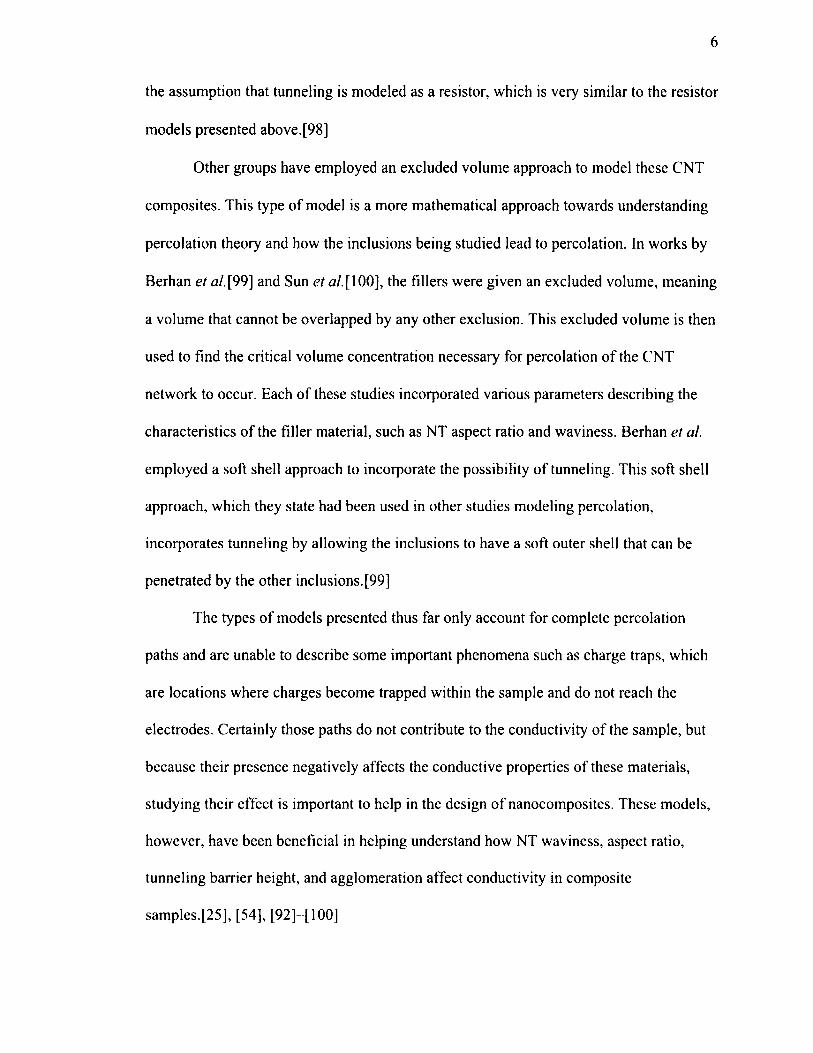
of composite materials.[109]—[113] A study in 1988 by Zeng et al. used Eq. (1.2) as the
effective medium approximation for the dielectric properties of a composite with two
materials having different dielectric properties.[113]
£ (0 )- £ (0) £ {0) - P (0)
P l + (1 ” P l) 4 ")+9 (4 ”’- 4 ”') = 0 (L 2 )
Here, px is the volume fraction of material one, £/ and are the dielectric functions of
materials 1 and 2 respectively, ee is the effective dielectric function of the composite
material, and g is a geometrical factor dependent on the shape of the inclusions. This
effective dielectric function is obtained by solving the above quadratic equation.
Other studies have also shown various mathematical formulations for other
effective medium approximations. In terms of electrical properties o f the composite, the
various formulations attempt to take into account the polarizability of each material,
along with some type of factor for the geometry of the inclusions. Each method is also
dependent on the volume fraction of the inclusion material. Effective medium
approximations lead to a simple usable quantity for describing how the composite
material, as a whole, will behave under an applied electric field. However, these methods
are not able to describe the local electric fields within a composite material that are
needed for this work.
In 1997, Cheng et at. performed a numerical study on two-dimensional samples
with various types of inclusions to understand how the electric field behaves in local
areas compared to an applied electric field.[108] In the study, Maxwell’s Equations were
used along with the dielectric constants of both materials in order to find the value of
local electric fields at 200 000 random points within a sample. The study showed that the
value of the local electric field inside the composite can be larger or smaller than the

9
applied electric field depending on the location within the sample. However, for the
various types of inclusions, a distribution of electric field values in the composite was
found to be between OE0 and 1.5E0, where E0 is the applied field, depending on the
relative dielectric constants of the matrix and inclusion materials. This study did state
however that there would exist so-called “hot spots” for the local electric field within the
sample and may tend to be near the edges o f the inclusion material if that inclusion
material is much more polarizable than the matrix material.
1.2 About This Work
In this work, a model is presented with the capability to study in depth how
various material properties affect charge transport within CNT composites, both before
and after percolation is reached. Routines have been developed to first generate virtual
composite samples and then to study charge transport within those samples using a
hopping algorithm similar to the hopping models mentioned previously. In addition, the
model has the ability to study samples large enough, in terms of size and number of
nanoinserts, to appropriately model system sizes in modem day micromanufacturing labs
without periodic boundary conditions in the transport direction. Incorporated into this
model are exceptional visualization capabilities through a program that has also been
developed in house, with details provided elsewhere.[114] This model can be used to
study how CNT waviness, CNT aspect ratio, sample size, dispersion, agglomeration, and
the host matrix all combine to determine charge transport within a CNT composite.
Besides modeling the transport process with routines written in the Matlab programming
language, calculations have been performed in various other modeling software packages
10
to better understand the underlying physics and to calculate parameters used in the
hopping model.
The routines that have been used for charge transport have gone through various
improvements throughout the progress of this work. These improvements are significant
enough to mention as they allow for larger composite samples, with more NTs, to be
simulated more efficiently. To the best o f this researcher’s knowledge, the routines
developed for these simulations allow the study o f samples with the number and aspect
ratio of NTs much larger than those capable with other models. [95], [100] This is
significant as CNTs are high aspect ratio nanofillers, and therefore in order to better
model them, one must be able to include very large aspect ratio CNTs in the simulation.
CHAPTER 2
GENERAL METHODOLOGY
Metropolis Monte Carlo routines have been developed in the Matlab
programming language so that they can be run on high performance computing systems.
The model in its current state was built on a previous version of the routines, which that
have been optimized on several levels. The contributions from this dissertation and how
they improve what was implemented beforehand, is indicated in the following sections.
It is well known that Monte Carlo simulation techniques can lead to results that
vary due to the randomness of the technique. In order to assure that results presented in
this work are statistically accurate, several replicas of the simulation box, all statistically
independent from each other, are created and the results averaged. In addition, certain
portions of the simulation processes have been parallelized in up to 12 parallel processors
in order to increase simulation efficiency. Simulations are composed of three main
routines: A generation routine, a neighbor finding routine, and a charge transport routine.
Overall, these simulations are generally performed on HPC servers. Two main clusters
have been used, the Cerberus cluster, which is a local Louisiana Tech University
supercomputer, and the Queen Bee 2 cluster available through the Louisiana Optical
Network Initiative (LONI). The Queen Bee 2 cluster is a 1.5 Petaflop system that was
commissioned in 2014. At that time, it was ranked as the 46th most powerful
supercomputer in the world.

12
Parameters necessary for these simulations were obtained using a set of other
codes and modeling algorithms that include Density Functional Theory, Green’s
Functions, and the fmite-element-based solutions of the Maxwell’s equations as
implemented in a number of commercial codes, particularly Gaussian 09[115], Atomistix
Toolkit[ 116], and COMSOL[l 17].
2.1 Generation of Virtual Nanocomposite Samples
In order to study electrical properties o f CNT composites, virtual samples are
generated to a specific size and with specific NT volume concentrations using a
Metropolis Monte Carlo algorithm. By growing to specific volume concentrations,
accurate comparisons can be made between various simulations.
To start this generation process, a sample of a certain length, width, and height is
partitioned into a three-dimensional mesh with the distance between each grid point equal
to the specified NT diameter. Therefore, the size of the NT determines the coarseness of
the mesh. A seed grid point is chosen randomly as the starting point for growing a NT. A
random walker then grows each NT segment by segment along the three-dimensional
grid. The random walker starts at the seed grid point and then “walks” to neighboring
points based on probabilities defined by user-specified input parameters. Grid points
define the start and end point of each o f the segments that make up a NT segment.
However, each segment can span a user-defined number of grid points. If a point that
already hosts a segment is chosen for growth, the choice is rejected and the segment is
regrown. All NTs are given a growth orientation in the x, y, or z directions. Waviness is
introduced by giving each new segment a probability, based on input parameters, to grow
13
along the specified orientation, or to deviate from that orientation. The waviness of NTs
is quantified through a waviness factor, WF, given in Eq. (2.1).
W F = 1 - (2.1)
Here ADt is the distance each NT spans along the specified orientation, Lt is the length of
NT i, and Nt is the number of NTs in the sample. Defined in this way, a higher waviness
factor indicates a sample with wavier NTs.
The algorithm to generate a nanocomposite sample that was described above is an
adaptation of the method reported by Evans et al.[ \ 18] In that work, aggregates of
nanofillers were generated into a volume space using a Metropolis Monte Carlo method.
Each nanofiller was considered one grid cell within the volume space and those grid cells
were filled randomly such that aggregates arise when neighbor cells were filled. For this
work, the same method was followed except that while growing a NT, subsequent cells
are randomly chosen, but only among cubes that are a neighbor of the last that was filled.
It is only when a NT is completed that a new random location is selected to begin
growing the next NT. Figure 2.1 shows a simple schematic o f this process.
Figure 2.1. Schematic representation of the NT’s growth process segment-by-segment. In the simulation, the boxes are considered completely occupied by the NT segment.

14
The generation of the NTs along a three-dimensional grid system allows the user
to generate samples in a very time-efficient manner. Other approaches have taken a
slightly different strategy to generating nanocomposite samples, in which NTs are still
grown segment by segment, but not on a grid system.[25], [95] In this way, NTs are free
to grow in any direction, with respect to the previous segment, within some limiting
values. The main issue in this method of generation is that after each segment is placed,
there is a need to check for overlap with neighboring NTs. This is an essential check if
accurate volume concentrations of nanofillers are to be reported. However, this type of
generation method can lead to time-consuming simulations, as NTs begin to repeatedly
overlap with pre-existing NTs at higher volume concentrations. By growing along a grid,
it is sufficient to check if the box where the next segment is to be place is already
occupied or empty.
Throughout the generation process, periodic boundary conditions are placed in the
two directions perpendicular to the applied electric field in order to minimize edge effects
at the sample boundaries. In order to do this, NTs are allowed to grow out one side of the
sample, and into the opposite side of the sample. In this way, there is a seamless growth
process, which essentially removes the boundaries of the sample perpendicular to charge
transport.
2.2 Finding nearest Neighbor Nanotubes
In order to be able to study charge transport, nearest neighbors must be identified
for each NT. If the minimum distance between 2 of the segments is smaller than a
maximum neighbor distance cutoff, then the NTs are considered neighbors. The
minimum distance and the points on each of the NT surfaces, where the distance is a
15
minimum are then stored. The neighbor distance cutoff in these simulations was typically
set at 2 nm, as that is generally where the probability for carrier hopping becomes
practically zero (see Section 2.4). The neighbor-finding routine has generally been the
most time-consuming portion of the entire simulation process due to the number of
calculations needed. As such, the neighbor-finding routine has been modified for this
work.
This routine first partitions the sample so that each NT is associated with some
portion of the sample. In the original version, only NTs in the same partition or a
neighbor partition are checked, in that way unnecessary comparisons between NTs that
are too far away are not unnecessarily compared. However, since the size of the partitions
must be such that whole NTs comfortably fit, but also needs to be an integer divisor of
the sample size, the minimum allowable partition size has generally been set equal to
around two times the maximum length of a NT. So even when only neighbor partitions
are considered, NTs in those partitions could be much further than the cutoff distance and
some unnecessary comparisons could be conducted. A work around was implemented
where each partition is allowed to overlap into surrounding partitions by the neighbor
cutoff distance. In this way, only NTs in the same partition (including the fuzzy
boundaries) need to be counted. Still, it is possible that a NT starts in one partition but
extends to a neighbor partition. In such a case, NTs in both partitions (including the fuzzy
boundaries) are included in the comparison. Figure 2.2 shows a schematic representation
o f the partitioning process.
16
All 4 Partitions Overlapped
Partition 2
Partition 4
Partition 1 Partition 3
Figure 2.2. Schematic representation of overlapping partitions for neighbor finding routine.
If the simulation is to be run on one processor, each NT can be assigned an
identity with its partition or partitions. Therefore, each new NT in the list is only checked
with other NTs that have the same identity. However, since these routines are setup in the
Matlab programming language, the built in parallelization techniques in Matlab have
been used in order to parallelize the neighbor finding routine so that it can be split into
the same number of processes as the number of partitions, thus decreasing the overall
simulation time. The routine has been coded such that a SPMD loop in Matlab can set up
a parallel processing pool with a specified number of workers, equal to the number of
partitions in the sample. In the Matlab programming language, an SPMD loop is a
parallel processing for-loop where each separate parallel processor performs the same
calculation. For example, if there is a calculation to be performed on a variable that has
1000 elements, then an SPMD loop with, for example, four processors can be used so that
each processor can perform 250 o f these calculations. Now one of the key components of
an SPMD loop is that each new calculation is not dependent on any calculations being
17
performed in each of the other processors. Once the 250 calculations have been
performed on each of the 4 processors, the resulting data can be recombined at the end of
the SPMD loop.
When these simulations are performed on an HPC system, the user must request a
certain number of processors for the simulation. This means that the user must know
exactly how many processors are to be used for a simulation for optimal usage of
resources. Within this portion of the simulation, the number of processors is generally set
up to be equal to the number of partitions needed for the sample, which is again based on
the length of each NT, as if one processor is being used. The one caveat here is that this
calculation, while simple, must be performed before beginning the simulation to know
the appropriate resources to request from the HPC system.
The maximum number o f parallel workers available with the current Matlab
licenses is 12, hence the samples can be either partitioned into either 1, 2, 4, 6, 8, or 12
partitions. Each worker in the Matlab parallel processing pool then takes a partition, and
finds the neighbors of each NT in that partition. For the case of a NT that crosses
partition boundaries, it will be checked on separate processors for neighbors in each
partition. There is then some necessary overhead in organizing the resulting neighbor
information gathered from each of the parallel workers so that it can be output to a file.
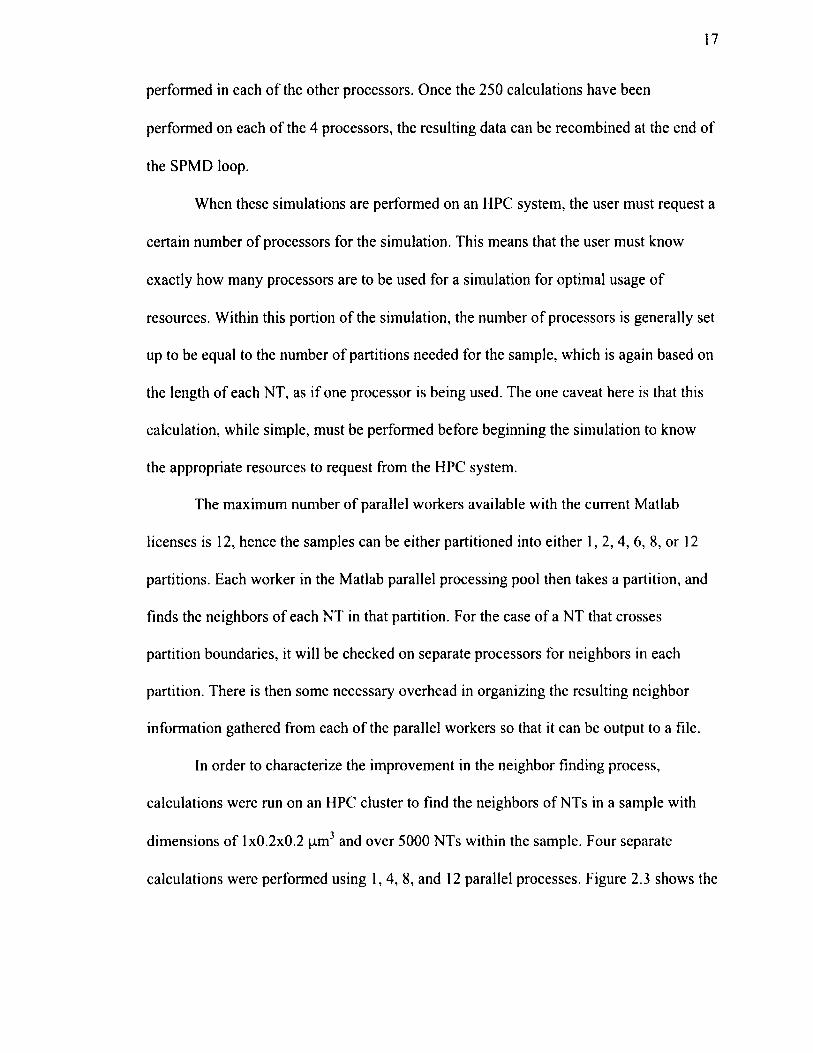
In order to characterize the improvement in the neighbor finding process,
calculations were run on an HPC cluster to find the neighbors of NTs in a sample with
dimensions of 1x0.2x0.2 pm3 and over 5000 NTs within the sample. Four separate
calculations were performed using 1, 4, 8, and 12 parallel processes. Figure 2.3 shows the

18
wall-time that each simulation took to manage overhead, split up processes, and then
combine the calculations done over the various processors.
50
£ 40
i 30
£ 20
§ 10
P a ra l l e l C o r e s
Figure 2.3. CPU wall times for calculating neighbor NTs for a specific sample with over 5000 NTs.
It can be seen that the amount of time to complete the calculation drops
significantly between 4 and 8 processors, illustrating how the use o f more parallel
processors can speed up the calculation of neighboring NTs. When 4 processors were
used, the simulation time went up by almost 10 hours. This illustrates the fact that if 1
processor is used, the number o f partitions is set based on the length of the longest NTs,
so that partitions may be of appropriate size to efficiently split up NTs into enough
partitions. Also, overhead was needed to set up the parallel processes or to recombine the
data post-parallelization. Additionally, 4 processors, and therefore 4 partitions, may not
have been the most optimal number of partitions. However, when 8 cores were used, NTs
were more efficiently sorted into partitions, and as a result, even with the overhead of
parallelization, the simulation time decreased to 7.79 hours. The wall time for twelve
processors was 7.73 hours, indicating that there would not be much improvement from
using 8 processors/partitions. In order to determine the appropriate number of processors

19
to use, the user would need to determine a number o f partitions such that each one is not
too small, or too large, and simulations can be parallelized efficiently. This improvement
to the model has been a recent development, and further improvements can be made, such
as allowing each parallel processor to handle multiple partitions instead of a single
partition.
2.3 Nanotube Length Distributions
In these samples, NTs can be grown with uniform lengths or with a given length
distribution. However, if a NT finds an obstacle to continue growing before reaching the
target length, after a few attempts, it is allowed to stop growing short of the target length.
This is a problem if a sample with equal sized NTs is being created, as some NTs will not
have the desired length. However, it can be seen in Figure 2.4a that this leads to a
distribution heavily peaked at the target NT length with a very low concentration o f NTs
o f other lengths, even at high concentrations. This problem is avoided or minimized
when samples with a given length distribution are considered by placing the larger NTs
first, so that if a particular NT cannot be placed and it is cut short, it will be counted
against the number of NTs to be generated at that shorter length. As seen in Figure 2.4b
where a normal distribution of tube lengths was attempted, the distribution of NT lengths
at different volume concentrations cannot be distinguished from each other. Distributions
shown in Figure 2.4 are averaged over 100 samples.

20
80%VI ■a. 70% £ -1% ms% 1s 60% ♦
1 50% • 10% X15%E 40%
^ 30% *20% *30%g 20%
■ s10%
0 5 10 15
# of Segm ents
20
45% i 40% I 35%VIU 30% I 25%
a 20%£ 15% ££ 10%° 5%
■1%
0%
5%
20%
25%
30%
0 10# of Segm ents
a) b)
Figure 2.4. NT length distribution (number of segments) presented as a percentage of NTs in the composite with a particular number o f segments (a) for a sample with NTs of uniform length (b) For a sample with NT’s length with a Gaussian distribution. In b) the different percentage cases are indistinguishable from each other.
2.4 Hopping Transport Algorithm
Once samples have been generated, virtual electrodes are placed on opposing ends
to apply an electric field in the x direction and begin the charge transport process. In the
hopping formalism, the electric field alters the energy landscape of the system so that
charge flow is biased in its direction.[103] Periodic boundary conditions (PBC) are
implemented in the directions perpendicular to the field. These particular set of boundary
conditions lead to a process where a carrier is injected into the composite from one
electrode and hops around in this 3D network until it is collected at the other electrode
located opposite to the injection electrode along the x direction. Then a new carrier,
statistically independent from the previous one, is injected. When, the carrier reaches one
of the sidewalls, PBC allow the charge to continue moving laterally. Using PBC, the
edges o f the sample are effectively removed so that charges are not confined to the lateral
dimensions of the sample, therefore minimizing edge effects.[119]

21
Over the course of this project, the hopping algorithm has undergone
modifications. In the original version, developed by a former student, some of the
parameters were used as fitting parameters. A contribution to the field of this dissertation
is the development of protocols to determine all fitting parameters from first principles or
known properties. However, the original approach (with fitting parameters) was used
extensively in the studies reported in Chapter 3 o f this work, and led to simulation data
that agrees well to experimental results. However, improvements were made to the
fundamentals of the hopping algorithm so that charge transport in the system is
completely dependent on the underlying physics o f the system without fitting parameters.
The remainder of this chapter will focus on the original routine. Chapter 4 goes into more
detail about the characterization of certain parameters, while also introducing the
improvements to the transport routine that have been made over the course of these
studies.
Within this version, the conduction is considered ballistic within the NTs, while
carriers hop between neighbor NTs across the smallest gap between them. The number of
neighbors for each NT, the (closest) distance to each of them, and the x-y-z coordinates
o f the point where the distance is a minimum are stored in a neighbor table.
The transport process starts by inserting a carrier from one of the electrodes into
one of the NTs in contact with that electrode. Then the hopping rate, 6)^-, to each of the
neighbor NTs is calculated as described in Eq. (2.2). A normalized cumulative
distribution function (CDF) is then constructed from these values to determine the
hopping probability to each of the neighbor NTs. Once the CDF is created, a random
number is sorted and compared to the normalized CDF to decide to which neighbor NT

22
the charge will transfer. In this way, charges are more likely to transfer to neighboring
NTs with higher associated hop rates.
_ A G °+ |A G ° | e d - E
Oiij = I Kyi e~ 2kBT e ksT (2.2)
In this equation, Ky is the transfer integral, accounting for the overlap of the wave
function of neighbor NTs and AG° accounts for the difference in the energy of the carrier
in the NT where it comes from and the energy of the carrier in the NT to which it hops.
e d - E is the work done by the electric field on the carrier (and thus the change in energy
of the carrier) as it moves a distance, d, inside a NT. T is the temperature of the system,
and k B is Boltzmann’s constant.
Vij in Eq. (2.2) the transfer integral is given by Eq. (2.3).
Vij = Joe ~aRii or \Vij\2 = v0e~2aRii (2.3)
Here, a is the tunneling coefficient and / ? y the distance between the two NTs, i and j ,
connected by the hop. The v0 term is the attempt-to-hop frequency and is dependent on
the electron-phonon coupling strength as well as the phonon density of states among
other material properties. Values for the attempt-to-hop frequency can be found in the
literature for conductive polymers (see for instance [107]), but these authors have been
unable to find values for CNTs. This attempt-to-hop frequency, however, is a pre-factor
that was used to set the time scale. For this version of the hopping routine, It was found
that an attempt-to-hop frequency of ~10V ‘ leads to a time scale in reasonable agreement
with experimental values in reference [120], so this value was used for all simulations
where this version was used. The exponential in Eq. (2.3) is the tunneling probability
derived from quantum mechanical calculations using the well-known Wentzel-K.ramers-
23
Brillouin (WKB) approximation in the limit of a high and wide barrier.[121] Indeed, the
host matrix material will have an effect on charge transport via the quantum phenomenon
of charge tunneling. Previous work has been done to quantify charge tunneling between
graphene sheets through a polymer layer where a 4-fold decrease in the tunneling
constant, compared to vacuum, was observed for Poly Acrylonitrile (PAN).[91] The same
process can be employed to calculate tunneling parameters for any material, giving the
model the capability to study how these various materials affect charge transport without
experimental input.
As said above, AG° in Eq. (2.2) accounts for the change in the carrier energy when
going from one NT to the next and it is given by Eq. (2.4).
€( and €j are the energy of the carrier in each NT. In all results reported in this
dissertation, all NTs are modeled as metallic NTs, thus carriers have energies that can
differ from the Fermi level with Boltzmann probability, as given in Eq. (2.5). This allows
Ef is the Fermi level and for this particular work it is considered the same in all NTs.
This is not a limitation of this model, but a choice for the calculations reported here as
each nanoinsert can be given its own Fermi Level.
The effect of an electric field on the carrier’s energy is accounted for by further
modifying the carrier energy e in each NT by the electrical potential energy provided by
the field, as can be seen in Eq. (2.6).
AG° = € i~ €j (2.4)
the charge carrier on a specific NT to have an energy slightly above or below the Fermi
energy level due to thermal affects.
(2.5)
24
AG° = €i - 6j - eExAx (2.6)
Here e* and e* are the energy of the charge in each NT taken from Eq. (2.5) before the
applied electric field is taken into account, e is the carrier, Ex is the x-component of the
electric field at each particular junction, and Ax is the distance the charge travels in the
direction of the field. Unlike the random energy fluctuations caused by temperature, the
electric field will result in a bias to charge flow in one direction. Notice that Eq. (2.6)
accounts for the effect of the electric field when the carrier hops across a junction
between NTs, while the second exponential in Eq. (2.2) accounts for the difference in
electrical potential energy between the point the carrier enters the NT and the point where
it leaves it to hop to the next NT. It should be noted that this exponential will either
exponentially increase or decrease based on the difference in the electrical potential
energy. It therefore becomes highly unlikely that a charge will attempt to move down a
CNT against the force o f the electric field.
The hop rates for the neighboring NTs calculated from Eq. (2.2) are then used to
determine a transition time for the carrier according to Eq. (2.7).
llEfO ( 2 j )tlJ 2> t, { ZJ )
Here, ( is a random number uniformly distributed between 0 and 1. The mobility of a
charge reaching the opposite electrode is calculated as in Eq. (2.8):
( 2 8 )
Where d is the distance across the sample in the direction of the electric field, t is the
total time it takes the charge to reach the collection electrode, E is the electric field, and
vdrift *s ^ e drift velocity. Each carrier moves through the sample until it reaches the
opposite electrode unless a specified time cutoff or maximum number of hopping

25
attempts is met. If one of those limits is reached, the charge is no longer tracked and a
new charge is generated. The mobility is averaged among those carriers that reach the
opposite electrode as shown in Eq. (2.9).
Here, n (c) is the total number of charges that crossed the sample.
The conductivity is calculated using Eq. (2.10) with the assumption that each NT
contributes carriers with the same concentration of 9 x l0 10 cm'2, which has been
calculated elsewhere for graphene sheets.[122] However, only those NTs that have been
visited by a carrier are considered to contribute to the carrier density of the sample.
Here e is the elementary charge, fiavg is the average mobility from Eq. (2.9), and n is the
carrier density, given by:
In equation (2.11), N is the number of NTs participating in conduction, r and L are
respectively the radius and length of NT i, ng is the carrier density of each individual NT
(calculated from the experimental value for graphene), and V is the total volume of the
sample.
The above formulation for charge transport has been used for many of the
simulations presented in this work. A few of the studies on charge transport in later
chapters incorporate some new characteristics into the charge transport routines. A
maximum hopping rate of 1 x 10⁴ s '1 has been found to give a good agreement between the
simulation and experimental results for NT composites within this study. This value is
(2.9)
* = neHavg (2 . 10)
26
much lower than the 1014 s '1 hopping rate that has been calculated for conductive
polymers.[105]
As the goal of this work was to form a predictive model for charge transport, the
ideal model would not need to fit simulation data to experimental data by scaling up or
down the pre-factor, v0. It was also felt that within this version the electric field was not
appropriately affecting charge transport. In addition, Eq. (2.2) is considered the hoprate
between the junctions, and the combination of hoprates for neighbors is placed into a
cumulative distribution function to determine the most likely hope to occur. Therefore,
the last exponential in Eq. (2.2) can cause the hoprate to exponentially increase towards
infinity if a charge were to travel a far enough distance through a NT in the transport
simulations. This then would cause the time for a hop, as calculated in Eq. (2.7) to be
zero, and not representative of the actual system. Therefore, it was in the best interest of
this work to formulate a better method, presented in Chapter 4, for calculating the
probabilities for various hops and then the time it would take a charge make those hops.

CHAPTER 3
EFFECTS OF MORPHOLOGY ON CONDUCTIVITY
One general limitation of most atomic and coarse grain simulation models is the
size of the sample that can be treated. Thus, it is important to determine how size-related
effects impact results and to find strategies to minimize those effects. In addition, there
are a number of geometrical properties which are tailorable within the fabrication of these
types of composite. These properties include the NT waviness, aspect ratio, and
agglomeration. In this chapter these issues are studied with the results presented below.
3.1 Nanotube Waviness and Aspect Ratio
Mobility and conductivity values were obtained for four samples with different
degrees of waviness. The sample dimensions were 100x50x50 nm3 with 0.5 nm diameter
NTs at a target length of 25 nm, leading to an aspect ratio of 1:50 (Figure 3.1).
27

28
c) d)
Figure 3.1. Waviness Factor equal to a) 0.31, b) 0.5, c) 0.67, and d) 0.71
The average mobilities (Figure 3.2) and conductivities (Figure 3.3) for the various
degrees of waviness in each simulation are shown below. Table 3.1 lists the fitting
parameters for the power law equation.
l.E-03l.E-04
^ l.E -05£?l.E-06o A£l.E -07l l .E -0 8 □oSl.E -09 O
l.E-10A
O
l.E-110 0.5 1
QO
A WF=0.31 □ WF=0.5 O WF=0.67 O WF=.76
0 0.5 1 1.5 2 2.5 3 3.5 4 4.5 5 5.5 NT Volume %
Figure 3.2. Mobility vs NT concentration as a function of waviness. The two greyed data points are below the percolation threshold. However, they represent the cases in which very few charges reached the opposite electrode (0.49% for WF=0.31 0.46% for WF=0.5) so the statistics on these points is very poor.
29
l.E-02
E l.E-04umjg l.E-06 '>1 l.E-08“DC
3 l.E-10
l.E-12
O WF=0.5
Power LawO
0.NT Volume Fraction
l.E-02
E l.E-04Uto
i.E-06;>
3 l.E-08"DC
u l.E-10
l.E-12
O WF=0.5
Power LawO
0.01 0.02 0.03 0.04 0.05NT Volume Fraction
l.E-03
l.E-05
tl l.E-07
O WF=0.768 l.E-09
Power Law
l.E-110.01 0.02 0.03 0.04 0.05
NT Volume Fraction
l.E-02
E l.E-04 u</?£• l.E-06
l.E-08O WF=0.67
U l.E-10 Power Law
l.E-120.01 0.02 0.03 0.04 0.05
NT Volume Fraction
l.E-02
l.E-03
l.E-04
§ l.E-05
£ l.E-06 .2| l.E-07 ■oo l.E-08 u
l.E-09
l.E-10
l.E-11
A
a * * * * * * *
A •• i f
........... PL WF=0.31
• * •.• i- 1
i» i
• 1
--------- PL WF=0.5
- • -PLW F=0.67
! -------PL WF=0.76■ i 1t 1 •
0.01 0.02 0.03 0.04 0.05
NT Volume Fraction
e)
Figure 3.3. Conductivity vs. NT concentration as a function o f waviness for (a) WF=0.31, (b) WF=0.5, (c) WF=0.67, and (d) WF=0.76 (e) Power law fits to conductivity values for each WF.
30
Table 3.1. Fitting parameters for the power law for varying waviness in NT composites.
WavinessFactor
<f>c (Volume Fraction)
t ac (S/cm) R-Square
0.31 0.0068 3.419 48.60 0.99160.50 0.0093 2.817 11.90 0.99750.67 0.0097 2.963 19.70 0.99820.76 0.0148 2.243 1.70 0.9995
The power law, Eq. (1.1), is dominated by the large volume fraction points where
tunneling is not a factor. Thus, it is natural that the curves in Figure 3.3a-d do not fit well
to the simulation data near the onset of percolation where tunnelling is dominant. Overall,
mobility and conductivity values increase with decreasing WF. This was expected as a
higher WF means the NT spans a smaller distance along the direction of the electric field,
forcing carriers to go through more NT-NT junctions to reach the collection electrode. In
addition, the percolation threshold shifts to lower values for decreasing waviness. This
trend has been seen elsewhere in the literature.[19], [123] More aligned NTs generally
have been seen to increase the charge transport properties of these composite materials.
These results indicate that the project was indeed capturing the physics of the system and
that results were comparing well with what has been seen in experimental works.
In order to study the effects o f NT aspect ratio, two simulations were performed
on samples with dimensions o f 100x50x50 nm3. All NTs had a 0.5 nm radius with a
maximum possible length of 25 nm and 37.5 nm in the first and second simulations,
respectively. These correspond to aspect ratios of 1:50 and 1:75. Charges were injected
into the sample under an applied electric field of 1 V/cm along the x-direction. The
conductivity of each sample is given in Figure 3.4 with the associated percolation power
law, given by Eq. (1.1), fit to the simulation result. The waviness factor is shown in

31
Figure 3.4 for each sample; notice that given the different aspect ratio, the waviness
factor differs slightly (0.31 for a 1:50 aspect ratio and 0.37 for a 1:75 aspect ratio). The
parameters for the associated power law fits are shown in Table 3.2.
l.E-02 -
l.E-03
l.E-04
.§ l.E-05
> l.E-06 I l.E-07
= l.E-08 o l.E-09
l.E-10
l.E-11
l.E-12 - 0
Figure 3.4 Conductivity for varying aspect ratios (AR) of 1:1:50 and 1:75 with the associated power law fittings.
Table 3.2. Parameters for the power law fits as a function of aspect ratio.
Aspect Ratio Waviness Factor 4>c(% Volume) t ac (S/cm)1:50 0.31 0.0063 3.415 48.601:75 0.37 0.0044 3.149 80.60
The conductivity is higher at all volume concentrations for higher aspect ratio
while the percolation threshold is shifted to lower concentrations, which is in agreement
with other authors [24], [25], [80], [99]. Values for the critical exponent fit into the
experimental ranges, which vary between 1 and 6.[19] It should be noted that there is a
slight variation in waviness in the two different aspect ratio cases in Figure 3.4. However,
the average difference between the curves for samples with WF 0.31 and WF 0.5 in
O AR=1:50 (WF=0.31) □ AR=1:75 (WF=0.37) — Power Law 1:50 Power Law 1:75
0.02 0.03 0.04NT Volume Fraction
32
Figure 3.3 is only 0.0003, while the average difference between the two AR curves in
Figure 3.4 is 0.001. This illustrates that the effect of the aspect ratio is much more
significant than the effect o f waviness in charge transport in nanocomposites. It also
shows that the difference in WF that was unavoidable in the calculations reported in
Figure 3.4 is minimal and the observed behavior is indeed attributed to the aspect ratio.
3.2 Agglomeration
As previously discussed, many experimental studies have shown that CNT
dispersion within a composite will play an important role in determining the electrical
properties of the composite.[25], [29], [31 ]—[34], [56] A major benefit to growing NTs
along a three-dimensional grid system, as discussed in Section 2.1, is the ability to easily
grow agglomerates or bundles of NTs. The grid system allows NTs to be grown directly
adjacent to previously grown NTs without greatly increasing simulation times because
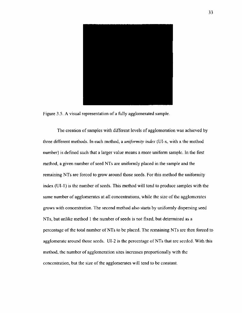
the grid points predefine the positions available for growth. Figure 3.5 illustrates a large
agglomerate in a sample demonstrating the ability of the routine to generate NTs into
agglomerates. The virtual electrodes are on opposite sides of the sample in the x-
direction.
33
Figure 3.5. A visual representation of a fully agglomerated sample.
The creation of samples with different levels of agglomeration was achieved by
three different methods. In each method, a uniformity index (UI-x, with x the method
number) is defined such that a larger value means a more uniform sample. In the first
method, a given number of seed NTs are uniformly placed in the sample and the
remaining NTs are forced to grow around those seeds. For this method the uniformity
index (UI-1) is the number of seeds. This method will tend to produce samples with the
same number o f agglomerates at all concentrations, while the size of the agglomerates
grows with concentration. The second method also starts by uniformly dispersing seed
NTs, but unlike method 1 the number o f seeds is not fixed, but determined as a
percentage of the total number of NTs to be placed. The remaining NTs are then forced to
agglomerate around those seeds. UI-2 is the percentage of NTs that are seeded. With this
method, the number of agglomeration sites increases proportionally with the
concentration, but the size of the agglomerates will tend to be constant.
34
In the last method, there are no seed NTs but each new NT is given a probability
(UI-3) to be placed randomly within the sample (as opposed to being placed near an
existing NT). Samples generated with this method are expected to have a less uniform
distribution, both in number and size of agglomerates, than the previous two methods. As
the probability increases, the sample becomes more uniformly distributed, so 0% means
fully agglomerated and 100% is fully uniform.
In this discussion on agglomeration, this work will refer to the number of seeds in
the first method, the percentage of volume as seed NTs in the second, and the probability
of growing in a random position in the third, as the uniformity parameter for the method.
With this choice, in all methods, a smaller value (number o f seeds, or percentage) means
less (and larger) agglomerates, while a large number means more uniform samples.
Figure 3.6 shows examples of how agglomerates grow with concentration with each of
the methods. Each row in the figure shows one of the methods, while the columns
correspond to concentrations of 0.01, 0.02, and 0.03 respectively. As can be seen, when
using the first method (Figure 3.6a-c), as concentration increases, agglomerate size grows
and percolation is achieved when agglomerates are large enough to connect to each other.
Figure 3.6d-f show that with method 2 the number of agglomerates increases with
concentration and percolation is achieved when there are enough to connect the two
electrodes. Finally, Figure 3.6g-i show a more disorganized sample. This is more obvious
at a lower concentration (Figure 3.6g).

35
Figure 3.6. Method 1 samples with 12 initial seed NTs are shown with periodic representation at concentrations of d) 0.01, e) 0.02, and f) 0.03. Method 2 samples with 5% of the required volume of NTs being dispersed randomly in volume concentrations of g) 0.01, h) 0.02, i) 0.03. Method 3 samples with each new NT having a 5% probability for uniform dispersion are shown with periodic representation at concentrations of a) 0.01, b) 0.02, and c) 0.03. In these plots a periodic image above and below the central volume is shown.

36
Samples with different degrees o f uniformity were created with the three methods.
The box dimensions in all cases were 50x50x50 nm3 with 0.5 nm radius NTs that had a
maximum length o f 15nm, or a 1:30 AR. For each configuration that was simulated, 64
independent copies of the simulation volume were generated. All results reported below
correspond to an average of all these configurations.
Using method 1, samples with 9 different UI-1, namely 0, 1,2, 4, 8, 12, 16, 20,
and 100, in addition to a uniformly distributed sample (MS), were created (group 1). For
simplicity in the notation, samples with uniform distribution, in which the number of
seeds is equal to the total number of NTs, and thus different for all concentrations, have
been nicknamed MS for maximum number of seeds. Samples created in this way are
equivalent to the 100% case in both of the other two methods. For method 2, simulations
were performed in which 1, 2.5, 5, 10, 25, 50, 75, and 100% of the required NT volume
fractions were randomly dispersed (group 2). Nine different degrees of agglomeration
were studied with method 3 (group 3). In these cases, each new NT had a 0%, 1%, 2.5%,
5%, 10%, 20%, 50%, 75%, or 100% chance of being placed randomly, as opposed to
near another existing NT. In the 0% case, only the first NT was placed randomly to
initiate the generation process.
The normalized fraction of charges that reached the collection electrode in groups
1, 2, and 3, and the mobility of those charges, are shown in Figures 3.7, 3.8, and 3.9,
respectively. The histograms were normalized such that the area under each curve is 1 in
all cases. This was necessary because the fraction o f charges reaching the electrodes is
significantly different at different concentrations and comparison becomes difficult.

37
0.3
0.25 s
0.15
0.05?
UI-1
b)
[Carriers ■ Mobility0.5
0.4-
0 .2 -
UI-1
a)
■■Carriers * Mobility0.3
0.25 t
0.05 s
UI-1
d)
! ■■Carriers ■■Mobility0.3
0 .2 5 1
0.2
0.15
0.05
UI-1
c)
Figure 3.7. Normalized values for the charges reaching the collection electrode and mobility of those charges for concentrations of a) 0.01, b) 0.02, c) 0.03, and d) 0.04 when using method 1.
0.5
UI-2
b)
0.6
0.3.
0 .2 f
UI-2
a)

38
{Carriers ■Mobility Carriers Up Mobility'
C) d )
Figure 3.8. Normalized values for the charges reaching the collection electrode and mobility of those charges for concentrations of a) 0.01, b) 0.02, c) 0.03, and d) 0.04 when using method 2.
[■C arriers ■Mobility1.2
1 >■
0.8 1J 0 6 - 1z
0.4. 10.2 I
n . . 1 ...........................................................................
0 1 2.5 5 10 20 50 75 100 UI-3
a)
[Carriers ■Mobility0.4
0.3
0.2
0.1
00 1 2.5 5 10 20 50 75 100
UI-3
0.6■Carriers ■ Mobility!
0.5
0.4
0.3
0.2
0.1
00 1 2.5 5 10 20 50 75 100
UI-3
Carriers ■Mobility
0 1 2.5 5 10 20 50 75 100
C) d)
Figure 3.9. Normalized values for the charges reaching the collection electrode and mobility of those charges for concentrations of a) 0.01, b) 0.02, c) 0.03, and d) 0.04 when using method 3.

39
The trend is consistent in all three methods. At the two lowest concentration
values, right below or on the onset of percolation (0.01 and 0.02), a larger number of
carriers reaching the electrodes, and higher mobilities, are found for samples with
intermediate UI values. Neither the disperse samples nor the heavily agglomerated
samples allow for many carriers to reach the collection electrode. For the lowest Ul in
methods 1 and 3, there is just a single clump in the box that is unable to bridge the gap
between the two electrodes. For method 2, UI-2—1 % corresponds to one or two
agglomerates, as there are between 100 and 200 NTs in that sample at these
concentrations, and it is possible that some transport occurs in some of the replicas.
However, the number of carriers reaching the electrode is still smaller than at larger UI
values. When fully dispersed, the NT-NT distance is close to the average distance
between neighbors for the sample, which at these low concentrations, is quite large even
for tunneling. Thus, carriers time out and are discarded, meaning the mobility is below an
acceptable threshold. Instead, when some agglomeration is allowed, the volume is more
efficiently utilized. By agglomerating, the NT-NT distance within the agglomerate is low
enough for conduction to occur and conductivity arises when these agglomerates are able
to connect to each other. The sample consists of voids and areas of higher density where
conductivity occurs.
For the larger concentrations, top of the percolation threshold (0.03 and 0.04), the
number of carriers reaching the collection electrode increases with the UI value, but the
mobility shows the opposite behavior. The concentration is large enough that there are
conduction paths formed regardless of the UI. In addition, a larger Ul value leads to a

40
larger number of parallel paths available for the carriers leading to the observed increase
in carrier collection. On the other hand, the larger the Ul, the further apart NTs are from
each other in each path, leading to a lower mobility. So at larger concentrations (top of
the percolation threshold), with larger UIs, more carriers are collected but with lower
mobility, leading to a tradeoff to be considered in the optimization of the composite’s
electrical performance.
Conductivity depends on the mobility, but also on the carrier density, which is
proportional to the number o f NTs that participate in conduction. The carrier density is
not the same as the number of carriers reaching the collection electrode. The number of
collected carriers does depend on the number of conduction paths available (which is
related to the number of participating NTs), but also on the characteristics o f those paths.
Conductivity values from samples in each group are shown in Figure 3.10a), b), and c),
respectively.
-*-0.01 -o-0 02-*-0.03-*-004
1 0 4 ■ ■ ■
-•-0.01 -c-0.02-*-0.03-*-0.04
1 2 4 8 12 16 20 100 MSUI-1
10 10 2 5 5 10 25 50 75 100UI-2
0 1 2 5 5 10 20 50 75 100UI-3
a) b) c)
Figure 3.10. Conductivity vs a) UI-1, b) UI-2, and c) UI-3 for four volume concentrations.
In all the cases and at all concentrations, the lowest conductivity is found for the
fully dispersed sample. The only exceptions are for UI-1 = 1 and UI-3=0 at the largest
concentration of 0.04. However, in those two cases, there is roughly just one large

41
agglomerate that in many cases cannot connect the electrodes. Conductivity becomes
more independent from the degree of agglomeration as concentration increases, which is
expected as percolation pathways become fully established and conductivity is less
sensitive to concentration. For UI-3, where agglomerates are random in size and number,
there is a more random behavior, particularly at low concentrations.
It can be inferred from Figure 3.10 that percolation begins to occur at lower
concentrations when there is agglomeration than for uniformly distributed samples. None
of the samples, regardless of the method used to create it, shows any conductivity in the
fully dispersed case at concentrations of 0.01. Thus, 0.01 is below percolation for
uniform samples. However, all three methods show some conductivity for intermediate
values of the corresponding Ul (even if for just one case as in method 3), showing that
the percolation threshold has indeed shifted down. The lower percolation threshold is
caused by the inserts forming localized, interconnected bundles that connect to both
electrodes so that charge tunneling is minimized in the agglomerates. This allows for
improved charge transport at lower volume fractions. A numerical study on percolation
of spheres and rods by Jadrich et al. has also shown this tendency towards a lower
percolation threshold with increased attraction between filler particles [124],
To further analyze conductivity, notice that for methods 1 and 3, smaller UI
values mean less seed NTs and thus, for a given concentration, agglomerates are larger
for lower UI leading to less interconnects among agglomerates. In addition, as the
relative size o f the agglomerate compared to the “hairs” increases, the conductivity
between interconnects becomes significantly lower than in the agglomerate and these
connections act as bottlenecks decreasing conductivity. This is evident in Figure 3.10a

and Figure 3.10b where conductivity is smaller for samples with large agglomeration
than for those with intermediate levels of agglomeration. This contrasts with the results
on method 2 where the agglomerate size is expected to be more uniform while the
number of agglomerates grows towards percolation. This leads to a more uniform
behavior o f the conductivity vs UI which monotonously decreases with UI at all the
concentration values studied here (Figure 3.10b). At the larger volume fractions, all of
the samples have reached percolation and it can be seen from Figure 3.10c and d, that
conductivity tends to be uniform across UIs (except maybe for extreme values).
For a perfectly dispersed sample, the concentration has to increase to a point
where the average distance between NTs allows for conductivity. However, if small
(nano-sized) agglomerates form, the NT-NT distance in the cluster is what controls
conductivity as long as agglomerates connect to each other to bridge the electrodes.
Agglomeration leaves voids in the sample in favor of localized bundles that connect to
each to each other through NTs at the edges that stick out like hairs.
As a visual aid to further understand the effect that these nano-agglomerates have
on charge transport, a sample with 8 initial seeds at a volume fraction of 0.01 is shown in
Figure 3.11. The NTs clearly form bundles that are interconnected. This figure was
produced with NTViz,[l 14] which is a GUI that also allows the user to highlight the
number o f times that each NT was visited by charges in the sample (Figure 3.1 lb). The
frequency of visits increases from blue to red. It is clear from Figure 3.11b and c that the
more heavily trafficked NTs are inside and in between the bundles. Notice also that the
group of NTs in the top-left of Figure 3.1 la, are not connected to the rest of the NTs and
therefore, are not visited by any charges.

43
c)
Figure 3.11. a) A sample at a NT concentration of 0.02 and initialized with 12 seed NTs. b) Each NT highlighted with a color that represents the number of visits each NT received, c) Zoomed in view o f the highly visited NTs within an agglomerate.
3.3 Sample Size
The previous two sections have looked at how characteristics of the NTs in the
composite affect conductivity within samples. However, any computational model of real
materials is limited in scope to the size of the virtual sample that can be modeled. This
section then focuses on changing the sample sizes in order to better understand how it
will impact simulation results.

44
Simulations were run on samples with lengths ranging from 10 nm to 400 nm,
with the dimensions perpendicular to charge transport kept constant at 100 nm. All
samples had relatively the same waviness factor and the maximum NT length was always
one half of the box’s length. This last constraint was to ensure that the NT-length-to-box-
side ratio was constant. Figure 3.12 shows a visual representation of the samples while
Figure 3.13 shows the power law fittings to simulation results for conductivity. Table 3.3
lists the fitting parameters for those fits.
Figure 3.12. Visuals for samples o f different lengths.
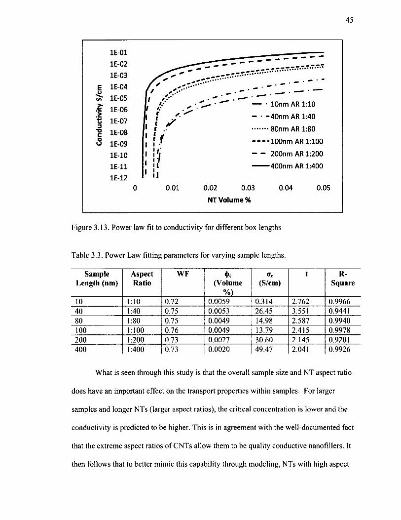
45
EUl/>z>tj3■DCou
IE-01IE-02
IE-03IE-04
IE-05
IE-06IE-07
IE-08IE-09
IE-10IE-11IE-12
- • lOnm AR 1:10
• -40nm AR 1:40
80nm AR 1:80
lOOnm AR 1:100
200nm AR 1:200
400nm AR 1:400
0 0.01 0.02 0.03 0.04 0.05
NT Volume %
Figure 3.13. Power law fit to conductivity for different box lengths
Table 3.3. Power Law fitting parameters for varying sample lengths.
Sample Length (nm)
AspectRatio
W F <|>c
(Volume% )
Gc(S/cm)
t R-Square
10 1 10 0.72 0.0059 0.314 2.762 0.996640 1 40 0.75 0.0053 26.45 3.551 0.944180 1 80 0.75 0.0049 14.98 2.587 0.9940100 1 100 0.76 0.0049 13.79 2.415 0.9978200 1 200 0.73 0.0027 30.60 2.145 0.9201400 1 400 0.73 0.0020 49.47 2.041 0.9926
What is seen through this study is that the overall sample size and NT aspect ratio
does have an important effect on the transport properties within samples. For larger
samples and longer NTs (larger aspect ratios), the critical concentration is lower and the
conductivity is predicted to be higher. This is in agreement with the well-documented fact
that the extreme aspect ratios of CNTs allow them to be quality conductive nanofillers. It
then follows that to better mimic this capability through modeling, NTs with high aspect
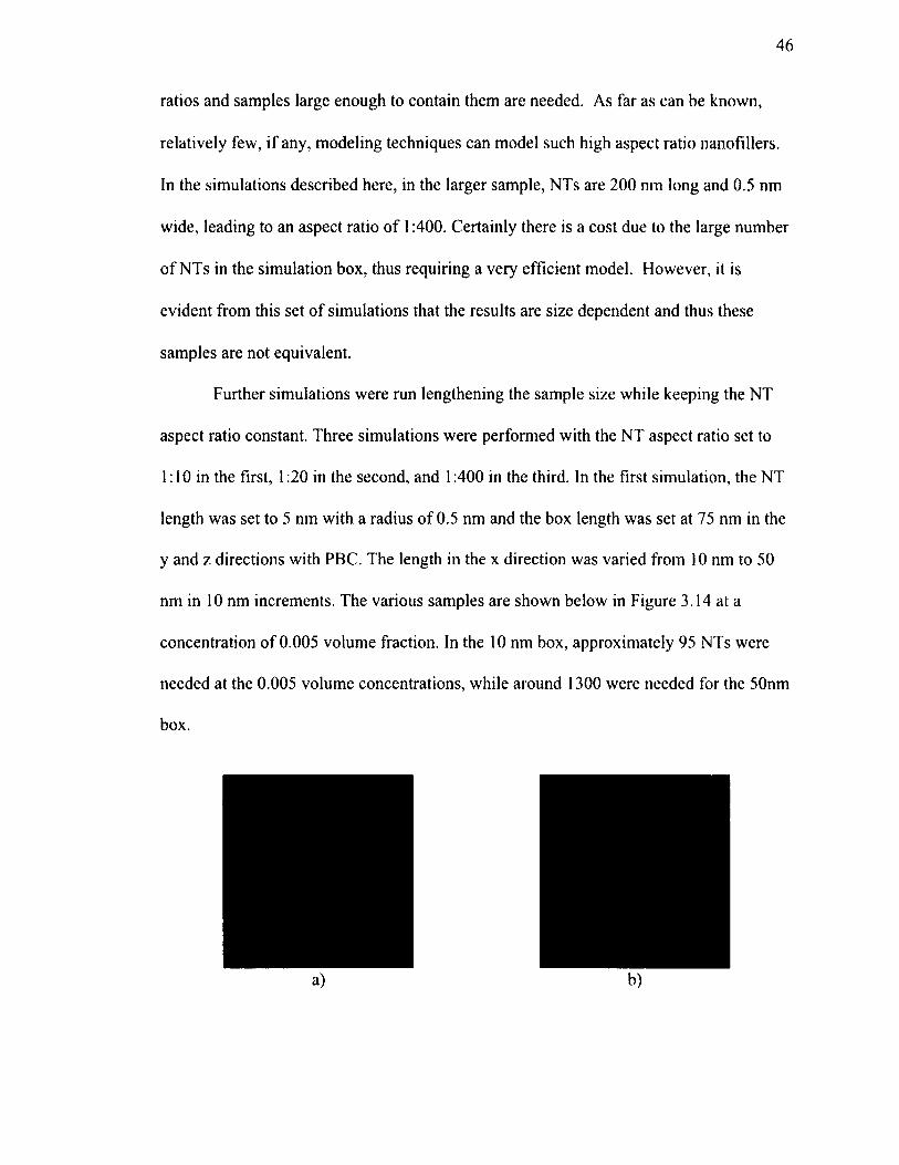
ratios and samples large enough to contain them are needed. As far as can be known,
relatively few, if any, modeling techniques can model such high aspect ratio nanofillers.
In the simulations described here, in the larger sample, NTs are 200 nm long and 0.5 nm
wide, leading to an aspect ratio of 1:400. Certainly there is a cost due to the large number
o f NTs in the simulation box, thus requiring a very efficient model. However, it is
evident from this set of simulations that the results are size dependent and thus these
samples are not equivalent.
Further simulations were run lengthening the sample size while keeping the NT
aspect ratio constant. Three simulations were performed with the NT aspect ratio set to
1:10 in the first, 1:20 in the second, and 1:400 in the third. In the first simulation, the NT
length was set to 5 nm with a radius of 0.5 nm and the box length was set at 75 nm in the
y and z directions with PBC. The length in the x direction was varied from 10 nm to 50
nm in 10 nm increments. The various samples are shown below in Figure 3.14 at a
concentration of 0.005 volume fraction. In the 10 nm box, approximately 95 NTs were
needed at the 0.005 volume concentrations, while around 1300 were needed for the 50nm

47
e)
Figure 3.14. Samples with 5 nm length tubes at 0.005 volume fraction with lengths of a) 10 nm, b) 20 nm, c) 30 nm, d) 40 nm, and e) 50 nm.
Figure 3.15 shows the conductivity results, with error bars. As the box length
increases, the conductivity does indeed decrease. However, the effect of size on
conductivity seems to decrease with the box’s length, indicating that these results are
beginning to converge to a specific value.

48
l.E-03
l.E-04
l.E-05
I l-E-06£ l.E-07 >’■§ l.E-08
g l.E-09 u
l.E-10
l.E-11
l.E-12
- * - 1 0 nm -Tk- 20 nm -* -3 0 nm
nmnm
0.01 0.02 0.03 0.04 0.05 0.06
NT Volume Fraction
Figure 3.15. Simulation results for changing the maximum box length while keeping the NT size constant.
In the second simulation with NTs of 1:20 aspect ratio, the NT length was set to
10 nm and the sample length was varied from 20 to 60 nm again in 10 nm increments
(Figure 3.16). In the 20 nm length box, 277 NTs were needed to reach the 0.015 volume
fraction, while 831 NTs were needed in the 60 nm length box.
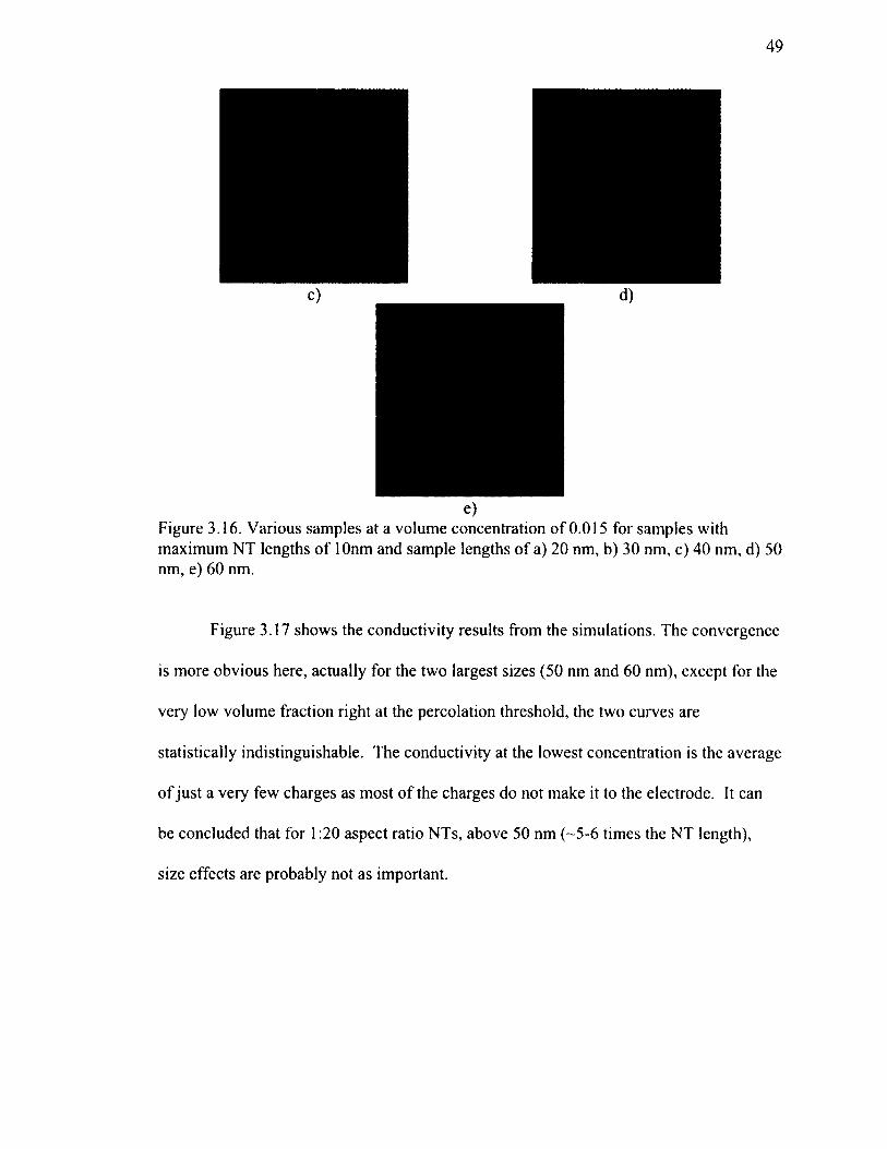
49
e)Figure 3.16. Various samples at a volume concentration of 0.015 for samples with maximum NT lengths of lOnm and sample lengths of a) 20 nm, b) 30 nm, c) 40 nm, d) 50 nm, e) 60 nm.
Figure 3.17 shows the conductivity results from the simulations. The convergence
is more obvious here, actually for the two largest sizes (50 nm and 60 nm), except for the
very low volume fraction right at the percolation threshold, the two curves are
statistically indistinguishable. The conductivity at the lowest concentration is the average
of just a very few charges as most of the charges do not make it to the electrode. It can
be concluded that for 1:20 aspect ratio NTs, above 50 nm (~5-6 times the NT length),
size effects are probably not as important.

50
IE-03
IE-04
IE-05
,5 IE-06i/>£ IE-07 ;>'■§ IE-08■DO IE-09
30 nm
IE-1050 nm
IE-1160 nm
IE-120.01 0.02 0.03
NT Volume Fraction0.04 0.05 0.06
Figure 3.17. Conductivity results for changing box length with NTs having constant length of 10 nm.
The 1:400 aspect ratio simulation was performed with much larger samples. The
NT length was set at 200 nm and the y and z dimensions were fixed at 100 nm with PBC
in effect (Figure 3.18). Figure 3.19 shows the simulation results. The longest sample
length was 1 pm in length, and was not run at all volume fractions due to memory
requirements for such large samples. In the 250 nm length sample, around 320 NTs were
needed to reach the volume concentration o f 0.005, while around 1300 were needed for
the 1 pm length sample.

51
e) f)
Figure 3.18. Samples with lengths of a) 250 nm, b) 300 nm, c) 400 nm, d) 600 nm, e) 800 nm, f) 1000 nm.

52
l.E-01
l.E-02
l.E-03
£ l.E-04t / i
l.E-05
• | l.E-06
-g l.E-07
3 l.E-08
l.E-09
l.E-10
l.E-11
I-■ -2 5 0 nm
- ♦ - 3 0 0 nm
- a - 400 nm
- * - 6 0 0 nm
800 nm
- • - 1 0 0 0 nm
0.002 0.004 0.006 0.008NT Volume Fraction
0.01 0.012
Figure 3.19. Conductivity results for changing box length with NTs having constant length of 200nm.
These results indicate that a statistically diverse sample is essential to obtain results
that are relatively unaffected by simply increasing sample size. As mentioned previously,
other models have resorted to PBC along the transport direction to achieve the same goal.
However, topological diversity cannot be ensured in that way. The main issue with PBC is
that if a charge reaches one end of the sample, it must continue into the periodic box from
the point it left the previous box, in many cases confining the charge to specific pathways.
This does not guarantee a quality sampling of various topologies that carriers would
explore in a real sample. Rather, it only guarantees that each inserted charge would see
many identical replicas of the same topology.
3.4 Comparison to Experimental Data with Preexisting Routines
The previous sections within this chapter have focused on simulations using the
preexisting transport routines. It was therefore necessary to validate simulation results

53
with experimental data. In the simulations in this chapter, the value for the tunneling
constant, a, in Eq. (2.3) was chosen to be 0.6 A '1, which has been calculated for Poly
Acrylonitrile (PAN).[91] As such it was of interest to compare simulation results with
experimental values previously presented in the literature for PAN/SWCNT composites.
Results from simulations on box sizes of 800x 1 OOx 100 nm3 and 1000x100x100 nm3 with
an applied field of 1 V/cm, were fit to the power law for conductivity, Eq. (1.1). Those
power law fits were then compared to experimental data by scaling vo in Eq. (2.3) by a
factor of 0.8 (Figure 3.20) essentially lowering the conductivity values from simulations
by 20%. These longer samples, with NT aspect ratios o f 1:400, were chosen for
comparison because they were statistically indistinguishable from each other while also
being some of the largest samples with maximum NT lengths at the time of the
comparison.
l.E+02
1.E+00£
^ l.E-02I Power Law 800nm
£ l.E-04O -------Power Law lOOOnm311 l.E-06 ■ Ref 125oo O Ref 120
l.E-08 <
l.E-100 0.05 0.1 0.15 0.2 0.25
NT Volume Fraction
Figure 3.20. Power law curves from simulation data fit to experimental data from works by Guo et al. [ 125] and Pradhan et al. [ 120]

54
The experimental values used for comparison were at much larger volume
concentrations than what are feasible with this model. As such, the power law fits had to
be extrapolated out to the experimental results, yet still agree well with the experimental
results. Most experimental works with PAN and CNTs focus on the formation of fibrous
bundles o f PAN/CNTs as in the work by Almuhamed et al. [126], and as such are not
necessarily comparable to the simulation results presented within this work. Further work
to characterize the tunneling constant, a, for different materials has been performed and
can be applied to this model for studies on other materials.
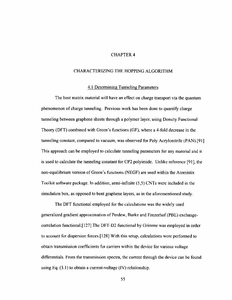
CHAPTER 4
CHARACTERIZING THE HOPPING ALGORITHM
4.1 Determining Tunneling Parameters
The host matrix material will have an effect on charge transport via the quantum
phenomenon o f charge tunneling. Previous work has been done to quantify charge
tunneling between graphene sheets through a polymer layer, using Density Functional
Theory (DFT) combined with Green’s functions (GF), where a 4-fold decrease in the
tunneling constant, compared to vacuum, was observed for Poly Acrylonitrile (PAN).[91]
This approach can be employed to calculate tunneling parameters for any material and it
is used to calculate the tunneling constant for CP2 polyimide. Unlike reference [91], the
non-equilibrium version of Green’s functions (NEGF) are used within the Atomistix
Toolkit software package. In addition, semi-infinite (5,5) CNTs were included in the
simulation box, as opposed to bent graphene layers, as in the aforementioned study.
The DFT functional employed for the calculations was the widely used
generalized gradient approximation o f Perdew, Burke and Emzerhof (PBE) exchange-
correlation functional.[127] The DFT-D2 functional by Grimme was employed in order
to account for dispersion forces.[128] With this setup, calculations were performed to
obtain transmission coefficients for carriers within the device for various voltage
differentials. From the transmission spectra, the current through the device can be found
using Eq. (3.1) to obtain a current-voltage (IV) relationship.
55

56
/ = f E / T C > [ / ( f ^ f ) - / ( f ^ ) ] dCi?) (4 .1 )
Here the summation is over each spin channel, e is the electron charge, T(E) is the
transmission coefficient per spin channel, f is the Fermi function of either electrode, TL
and Tk are the temperatures of the left and right electrodes, and n L and fiR are the
chemical potentials o f the left and right electrode, which are related to the applied voltage
bias as in Eq. (4.2).
Hr ~ H l = eVbias (4.2)
Previously, it has been seen that, for a constant Vbias, the carrier transmission rate
exponentially decays with distance through a non-conducting region.[91] As such, the
current-distance relationship can be approximated by Eq. (4.3).
1 = Ae~2ad (4.3)
Here A is a constant determining the maximum amplitude of the current, a is the
tunneling parameter, and d is the distance through the insulating region. The exponential
term in Eq. (4.3) can be found directly by using the Wentzel-Kramers-Brillouin (WKB)
method for approximating the transmission probability for a particle encountering an
energy barrier. In a simple system where the particle and barrier energy do not change as
a function of x, a is a measure of the tunneling barrier height, V relative to the energy, E,
of the particle. In the limit of a high and wide energy barrier, V is much larger than E and
the transmission probability exponentially depends on the barrier width.[ 121] Thus, for
wide and tall barrier, the current versus tunneling distance can been approximated by Eq.
(4.3).
To characterize a for other materials, the current voltage relationships for various
devices were fit to Eq. (4.3) using a and A as the fitting parameters. If the process is

57
purely tunneling, then the natural logarithm of the current has a linear relationship with
the distance between the NTs as in Eq. (4.4). Therefore, a simple least squares fit
algorithm can be used to fit the current-distance relationship. In this work, the Matlab
Curve Fitting Toolbox was used as the fitting tool.
log(/) = log04) + 2 ad (4.4)
Within this work, most of the simulations reported assumed the matrix material to
be Polyacrylonitril (PAN) since the tunneling constant for this material and experimental
conductivity values were readily available for PAN/CNT composites. However, in the
interest of further validating this model and to illustrate its capability, the tunneling
constant of other polymeric materials was needed. A study performed in 2003 by Ounaies
et al. was selected as a possible experimental work to compare with simulations. In that
work, the matrix material was CP2 Polyimide with single walled CNT inclusions.[88]
To begin the process to characterize a for this system, a single CP2 Polyimide
monomer (Figure 4.1) was built and its geometry optimized using DFT calculations in
Gaussian 09’. The B3LYP functional with the 6-31G basis set was used. The optimized
structure was then ported into the Atomistix Toolkit software package.
Figure 4.1. Optimized CP2 molecule within Gaussian 09'.

58
This monomer was then placed in between two metallic CNTs in various
configurations in order to sample various arrangements o f this polymer/CNT interface.
The first configuration contained a single CP2 monomer placed in between the two CNTs
as in Figure 4.2.
Figure 4.2. Single monomer of CP2 Polyimide between two metallic CNTs.
The calculation was repeated with two and then with three monomers within the
junction. In order to do this, the CP2 molecules were rotated before being placed within
the device. These first configurations are thus termed the “rotated” devices. Within each
new device, the central region was optimized, with the CNTs being held fixed to speed
up simulation times and provide structure to the device. For these devices, shown in
Figure 4.3, the initial configurations were such that the distance between CNTs was 1 nm
for the single monomer, 2 nm for the 2 monomers, and 3 nm for the 3 monomers.
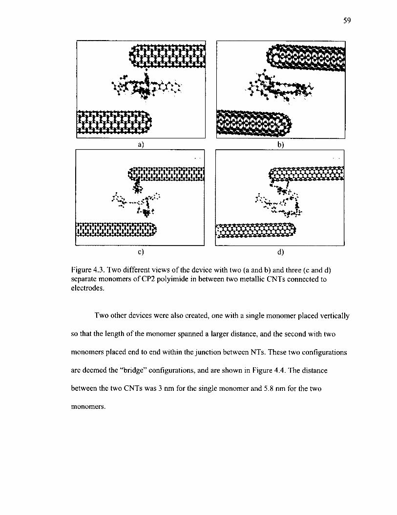
59
b)
•»** /V r . ,
<^i»* * t t »‘ i"1* •". • lA #
d)
Figure 4.3. Two different views o f the device with two (a and b) and three (c and d) separate monomers of CP2 polyimide in between two metallic CNTs connected to electrodes.
Two other devices were also created, one with a single monomer placed vertically
so that the length of the monomer spanned a larger distance, and the second with two
monomers placed end to end within the junction between NTs. These two configurations
are deemed the “bridge” configurations, and are shown in Figure 4.4. The distance
between the two CNTs was 3 nm for the single monomer and 5.8 nm for the two
monomers.

60
a)
Figure 4.4. a) 1 and b) 2 monomers stretched end to end bridging the gap between the two metallic CNTs.
The current vs. tunneling distance for both the rotated and bridge configurations
are shown in Figure 4.5 with the current shown in log-scale. There is a clear exponential
decay with both the rotated and bridged configurations as the junction distance between
the two CNTs increases, as expected. It can also be seen that the two configurations also
lead to similar decay rates, which was also expected since the same molecule is bridging
the junction gap, just in different orientations.
X- O.lV-Rot. 0.7V-Rot. • •A - - O.lV-Bridge - ■ - 0.7V-Bridge
< IE-05c
c<uIE-11
uIE-17
IE-230 20 40 60
Junction Distance (Angstroms)
Figure 4.5. The current-distance relationship for the rotated configurations and the bridged configurations at the various distances.

61
The tunneling constants for the rotated configuration and the bridged
configurations are shown for varying voltages in Table 4.1. The current-distance
relationships for voltages of 0.3 and 0.5 were not plotted in Figure 4.5 to avoid
convolution within the figure.
Table 4.1. Tunneling constants, a, for various voltages in the rotated and bridged configurations.
Bias (V) a (1/A) - Rotated a (1/A) - Bridge0.1 0.4934 0.54120.3 0.4879 0.52300.5 0.4831 0.50440.7 0.5004 0.5308
It can be seen that, overall, the change in a with voltage overall is minimal.
Therefore, the average a for all biases in all configurations was obtained so that an
average tunneling constant could be used for future studies within transport routines. For
CP2 Polyimide, the tunneling constant to be used in transport routines would be 0.5068.
This same process can be used to characterize the tunneling constants for other materials.
4.2 Charge Transport through Junctions.
Intuitively, the maximum hopping rate, or transition rate, in a junction between
NTs is essentially the number of times per second that a charge would attempt to move to
the neighboring conductive site. The hopping rate in this model will be at the maximum,
or equal to v 0, when two conductive sites are such that the tunneling distance for a charge
is considered to be zero, and AG° in Eq. (2.2) is equal to zero. Since the formulation of
time in hopping models involves taking the inverse of the hopping rate, it intuitively
makes sense that one could determine the time it would take for a charge to move through

62
the contact resistance between two CNTs and then take the inverse of that time to find the
transit rate. Ohm’s Law, which is given in Eq. (4.5), can be used as a classical
representation of the time d t it would take and amount of charge dq to move through a
contact resistance, R, between two CNTs.
Equation (4.5) can be rearranged so that d t can be represented by Eq. (4.6).
d t = ^ = vo_1 (4-6)
Where the voltage, V, can be written in terms of the local electric field across the resistor,
dq in this case can be represented as the value o f one charge, and d is the distance across
the resistor. Therefore, the maximum hoprate, v0, will be equal to d t -1 when two NTs are
in contact with each other, and proportional to the electric field between the two CNTs.
This is significantly different from the original version of the transport routine as the
electric field has an increased effect on charge movement by altering the maximum transfer
rate.
The estimation of the value of the contact resistance between two CNTs varies
T Owithin the literature between 10 and 10 Q.[129] In order to obtain a specific value of the
contact resistance between two CNTs, ab initio calculations were performed on the
device shown in Figure 4.6 in Atomistix Toolkit using DFT. The GGA PBE functional
with the Grimme DFT-2 dispersion correction was used to obtain the current-voltage
relationship, as previously discussed in Section 4.1. Both CNTs in the above figure are
armchair CNTs, meaning that the chiral vector (m,n) was such that m and n are equal, in
this case (5,5). Since m and n are equal, the CNTs were expected to behave as metallic
objects in the device. [2] The distance between two graphitic carbon sheets has been

63
found to be around 3.414 A.[130] However, within polymeric materials, the CNTs may
be forced to be closer or may actually be farther apart than this distance. A full
optimization of the CNTs could be performed in order to find this distance. However, as
an approximation, the two CNTs were placed in the sample so that the minimum distance
between them was around 3 A.
Figure 4.6. Two armchair CNTs distanced approximately 3 A apart to calculate the contact resistance between two metallic CNTs.
The current-voltage relationship for the device, shown in Figure 4.7, clearly
indicates Ohmic behavior, which was to be expected for the two metallic CNTs separated
by a junction resistance. A linear fit of the I-V relationship led to a value of 1.754xl06 Q
within the device, which is well within reported experimental values of the contact
resistance for CNTs.[129] With this value for the resistivity, the transit time for one
charge moving through the above resistor, using Eq. (4.6), would be 9.366x1 O'6 s for an
electric field of 1 V/cm within the junction. Using this transit time, the number of times
per second that one charge would move through this resistor would be 1.067x10⁵ s '1.
64
4.5
4
3.5
■ 10 "
------♦ ATKData
0)I 2 .5
c ^ «3 1.5 O
1
0.5
l=V/RR=1 754X106 R-Square 0.998
Oif-0.1 0.2 0.3 0.4
Voltage0.5 0.6 0.7
Figure 4.7. Current versus voltage for the device with two armchair CNTs.
As a side note, this new method for parameterizing v0 leads to a maximum
transfer rate that is proportional to the voltage in the junction between two NTs. In the
original version of the transport routine, v0 was a constant. Within these simulations, if
the voltage between two CNTs is constant, then v0 will remain a constant. However, if
the local voltages across the junction resistance vary, then v0 will also vary. More work
to validate this method for calculating v0, and characterizing the voltage in these types of
contact junctions will be discussed in the future works section of this work. However, it
will be shown later in Chapter 5 that considering the same electric field in all junctions
does lead to acceptable results as long as the value of that field is equal the average of
field among all the junctions, which happens to be a few times larger than the applied
field.

65
4.3 Charge Transport throufih CNTs.
Historically, hopping algorithms being used for charge transport in
semiconducting materials and conductive polymers dealt with charges that are localized
to sites. Previous hopping studies generally have not needed to take into account
delocalized carriers, or carriers that are allowed to move around in localized confined
regional03], [104] In the hopping algorithm presented so far in this work, the carrier is
given the ability to move along the conductive NT. In the version of this hopping
algorithm presented in Section 2.4, each CNT was considered to promote ballistic carrier
transport, and therefore it was approximated that the time it would take a carrier to move
through a CNT would be negligible when compared to the time of the hop between NTs.
In this way, the hopping algorithm would only be concerned with charge hopping
between the NTs, much like other hopping algorithms previously discussed. In reality,
the CNT will have an intrinsic resistance and it will take the carrier some amount of time
to move through the CNT over a specified distance. This time can be approximated using
the classical equation for Ohms law, as described below.
It is a known phenomenon that any ballistic transport process will be limited by
the quantum of conductance, G0, given in Eq. (4.7).[7], [131], [132]
2e2Go = X (4.7)
Here, e is the value of the electron charge and h is Planck’s constant. The factor of 2
accounts for the degeneracy of the electron spin. This quantum of conductance is the
maximum conductance, or minimum resistance, that can be obtained in a 1-D channel
separating two ideal contacts at very low temperatures. It arises in systems where the
distance to be traveled by the charge is much smaller than the mean free path of the
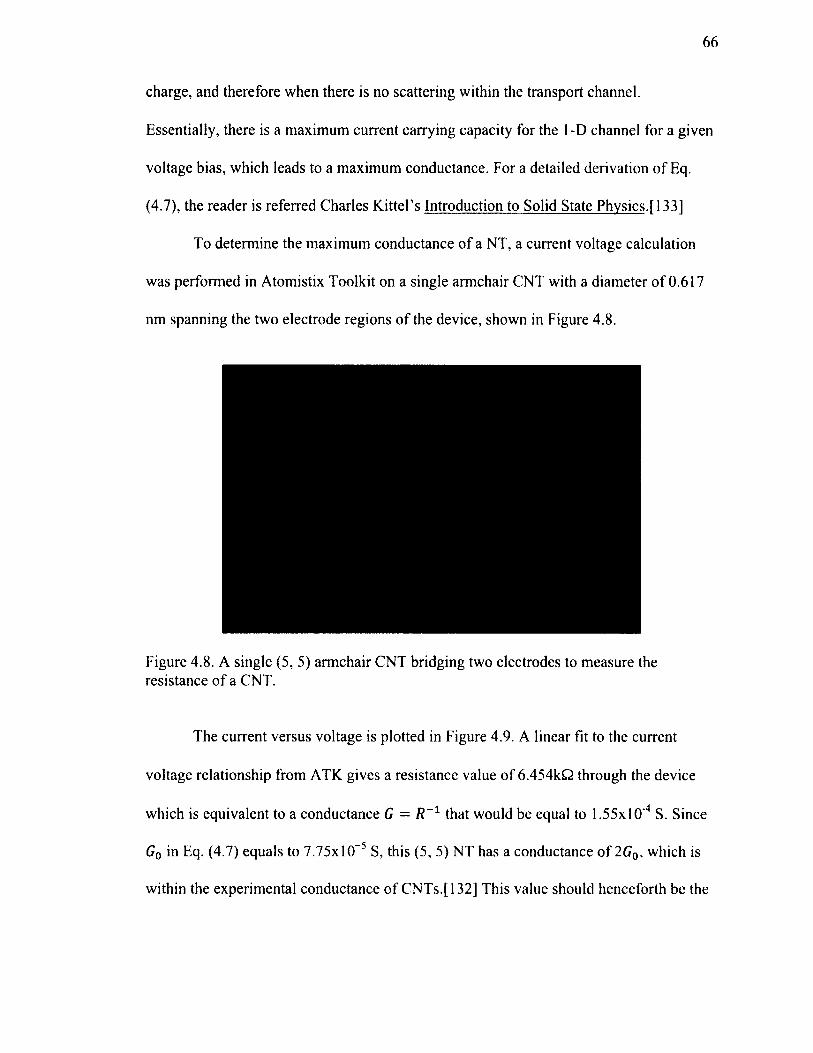
66
charge, and therefore when there is no scattering within the transport channel.
Essentially, there is a maximum current carrying capacity for the 1 -D channel for a given
voltage bias, which leads to a maximum conductance. For a detailed derivation of Eq.
(4.7), the reader is referred Charles Kittel’s Introduction to Solid State Physics.f l33)
To determine the maximum conductance of a NT, a current voltage calculation
was performed in Atomistix Toolkit on a single armchair CNT with a diameter of 0.617
nm spanning the two electrode regions of the device, shown in Figure 4.8.
Figure 4.8. A single (5, 5) armchair CNT bridging two electrodes to measure the resistance o f a CNT.
The current versus voltage is plotted in Figure 4.9. A linear fit to the current
voltage relationship from ATK gives a resistance value of 6.454k£2 through the device
which is equivalent to a conductance G = R _1 that would be equal to 1.55x10"4 S. Since
G0 in Eq. (4.7) equals to 7.75x10⁻⁵ S, this (5, 5) NT has a conductance of 2G0, which is
within the experimental conductance of CNTs.[132] This value should henceforth be the
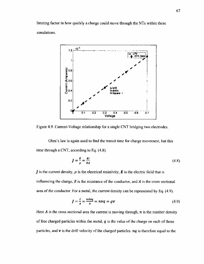
67
limiting factor in how quickly a charge could move through the NTs within these
simulations.
• 10'4
^rjF R -4 ATKData
< 0.6
l=V/RR=6454 R-Squara: 1
5 0.4
0.2
0.2 0.3 04 0.5 0 6 0.7Voltage
Figure 4.9. Current-Voltage relationship for a single CNT bridging two electrodes.
Ohm’s law is again used to find the transit time for charge movement, but this
time through a CNT, according to Eq. (4.8).
/ is the current density, p is the electrical resistivity, E is the electric field that is
influencing the charge, R is the resistance of the conductor, and A is the cross sectional
area of the conductor. For a metal, the current density can be represented by Eq. (4.9).
f 1 nAv(l rvx/ = - = — = nvq = pv (4.9)
Here A is the cross sectional area the current is moving through, n is the number density
of free charged particles within the metal, q is the value of the charge on each of those
particles, and v is the drift velocity of the charged particles, nq is therefore equal to the

68
charge density, p within the conductor. This generalized version of Ohm’s law can be
rewritten as in Eq. (4.10) in order to find the drift velocity of charges moving through the
conductor.
V = ^ (4.10)
In the transport routines with NTs, it is assumed that E is the applied electric field along
the x direction, I is the length of the NT, A is the cross sectional area of the NT, and q is
the charge density within NTs. q is the carrier density for the individual CNT, calculated
using the carrier density for graphene, ng , taken from Eq. (2.11). From the drift velocity
the time t it takes a charge to move through the conductor can be found through Eq.
(4.11).
t = V (4.11)
Here, Ax is the distance the charge moves along the x-direction under the influence of the
applied electric field, which in this case is the distance between the point where the
charge enters the NT and the point where the charge exists the NT.
4.4 Improvements in the Transport Algorithm
In order to incorporate the calculations presented in Sections 4.2 and 4.3, the
hopping algorithm was altered as described below. The probability for hops to occur is
still governed by Eq. (2.2). However, Eq. (2.2) is deemed a pseudo probability as the
exponential calculating the effect of the electric field can allow this value to
exponentially increase. The individual values between each neighboring NT are compiled
into a normalized cumulative distribution function. The next NT to hop to is then chosen
69
according to this cumulative distribution function and a sorted random number. Thus far,
this is no different than the original version of the transport algorithms.
In that version of the transport algorithm, the hopping rate, Eq. (2.2) was the term
used for the calculation of the transit time. However, because the hopping rate
exponentially increases with NT length or with the electric field, due to the last
exponential, the transit time can decrease exponentially. This means that the maximum
drift velocity for charges will have an infinite limit, and could be larger than the
maximum conductance of the conductive filler, as calculated in Section 4.3, would
predict. Therefore, it was of interest to separate the calculation of time into two parts. The
first is the time for hops to occur, and second is the time it takes for a charge to move
through a NT. Therefore, the actual hopping rate used for calculating the time for a hop is
similar to Eq. (2.2), except that the last exponential term is removed, leading to Eq.
(4.12). In this way the time calculated from the hopping rate accounts for the time
involved in the hop from NT to NT and not the transit time in the NT.
A G °+ |A G °|
( i ) i i T i m e = V 0 e ~ 2 a R l t e 2kBT (4-12)
The time, t, for a charge moving through the CNT can then be calculated using Eq.
(4.11). Therefore, the total time, T, for the charge to move down the CNT and then to
transit from one NT to a neighboring NT can be written as in Eq. (4.13).
t = ln(0 + t (4.13) U>i)Tim e
The first portion of Eq. (4.13) is taken from Eq. (2.7), but using Eq. (4.12) instead of Eq.
(2.2). The additional time t then incorporates the maximum conductance allowed through
an ideal CNT.

70
Still one major problem remains that needs to be solved, which is how to deal
with the statistically possible case of a carrier moving in the CNT against the electric
field. This is possible due to the nature of the Metropolis algorithm that allows an
energetically unfavorable move, with Boltzmann probability. Such a move in the
direction of the field has been predicted in conductive polymers with geometrical
disorder, as traps in the sample may make going around (and thus against the electric
field in some regions) more favorable. The problem is that if the current algorithm were
used, the time t calculated using Eqs. (4.9) to (4.11) would be negative. So the task then
becomes finding a suitable means of calculating this time for carriers moving against the
field.
If there is no applied electric field, the carrier would be equally likely to move in
either direction along the NT. Upon applying an electric field, carriers will on average
move in the direction of the field. The term governing the change in energy due to a
carrier moving down the NT under an electric field is given by Eq. (4.14).
e kBr (4.14)
This factor will lead to an increased hopping rate for carriers moving down the field and a
decreased hopping rate for carriers moving against the field. Since the transit time is
obtained as the inverse of the hopping rate a ratio between the factor in Eq. (4.14) for
down the field transport to the same factor for up the field transport through the same
distance should be proportional to the ratio between the up-the-field transit time to the
down-the-field transit time. In other words,
71
q E d cp T f f r q E ( d F - d B ) q & E 2 d
Pf b = - 5 1 3 J= e = e W = ' f (4.15)e W F
since in this case dB is equal to — dF, which is equal to 2d, where d is the distance
travelled by the carrier. Now, the transit time for carriers moving against the electric field
can be calculated as in Eq. (4.16).
= Pfb * tp (4.16)
Here, tF is the time t obtained from Eq. (4.16) and PFB is the ratio given by Eq. (4.15). In
this way, the time penalty for a charge moving through the NT against the electric field is
proportional, by a factor that is proportional to the ratio of the hopping rate, to the time it
would take the charge to move along the direction o f the electric field if the charge had
chosen a forward path of the same distance. As the travelled distance for backwards
movement increases, or the electric field increases, the time penalty for making a
backwards hop increases.
In fact, this formalism can be generalized if dB in Eq. (4.15) is replaced by d T
where d T is the distanced travelled by the charge inside the NT which is numerically
equal to d F, but positive for forward transport and negative for backwards transport. In
that way, Eq. (4.15) can be rewritten as in Eq. (4.17).
Pfb —' q E 2 d p
e kBT f o r backw ard tra n sp o rt (4.17)1 f o r fo r w a r d tra n sp o r t
Then the time t for this movement can be rewritten as in Eq. (3.18).
£ = Pfb * tp (4.18)
Now, the total time for a charge to move from one NT to another can remain in the form
of Eq. (4.13), with t being given by Eq. (4.18). This, along with v0 being calculated using

Eq. (4.6), allows the entire algorithm to be based on first principles, as intended, in
of capturing the full physics of the system without experimental parameterization.

CHAPTER 5
EFFECTS OF THE LOCAL AND APPLIED ELECTRIC FIELDS
The majority of the simulations in Chapter 3 were performed using the original
version of the model. Within that version, it was assumed that, on average, the local
electric fields within the NT-NT junctions would be equal to the applied electric field.
Even though this version did see good agreement with experimental works, it was
decided that this assumption needed to be tested in order to see if it indeed is a valid
assumption. The study by Cheng et al., which is discussed in more detail in Section 1.1,
found that the distribution of the x-component of the local electric field, sampled from
random locations within the composite, was peaked either above or below the value of
the applied electric field, depending on the relative dielectric constants of the matrix and
filler material. The study indicated that the majority of the values of the local field would
not be much different than the applied electric field. However, it was also mentioned that
there may exist locations within the composite where the electric field may be much
larger than the applied field, but those locations were not classified within the study.[108]
The study by Cheng et al., while very helpful and informative, was only done for
two dimensional materials and relatively low aspect ratio inclusions. As such, simulations
were performed in COMSOL, a finite element based simulation software, in order to
determine the local electric fields for various composite materials. The study described
below in Section 5.1 differs from the one by Cheng et al. in that it is done in a three
73

74
dimensional system made to replicate the composites simulated in this work. It also
focuses on the electric fields within the junctions between neighboring inclusions in
addition to the distribution of local electric fields throughout the sample.
5.1 CQMSQL Studies on Local Fields
Within this work, the hopping model presented previously only considers direct
current, where the composite is subjected to a constant electric field. As such, the
underlying physical equations to be solved by COMSOL are Maxwell’s equations under
the assumption that the magnetic field, B , and displacement field, D, do not vary in time.
V y . H = J + ™ (5.1)
» x £ = ^ (5.2)
V • D = p (5.3)
V B = 0 (5.4)
With
dD „ dB<5-5>
The fact that the curl of E is equal to zero in the electrostatics case leads to Eq. (5.6).
E = - W (5.6)
Where V is a scalar potential, in this case the electric potential. Inside a dielectric
material, the electric displacement, D, can be found as in Eq. (5.7).
D = e0E + P (5.7)
Here, e0 is the permittivity of vacuum and P is the polarizability of the material. If the
dielectric material is assumed to behave as a linear dielectric, then P becomes
proportional to the electric field, as in Eq. (5.8).

75
P = CoXeE (5.8)
Where e0 is the permittivity of vacuum and Xe is *he dielectric constant of the material.
This then results in the displacement field, D, being proportional to the electric field, E,
as in Eq. (5.9).
D = eE (5.9)
Which leads to Eq. (5.10).
V - e E = p (5.10)
Where e = e0 + e0x e and is the permittivity of the material. This combined with the fact
that the electric field, E , is equal to the negative gradient of a scalar potential allows the
above equation to be manipulated into Eq. (5.11).
V - e ( - V V ) = p or V2V = (5.11)
Which is the traditional form of Poisson’s Equation in a linear dielectric material. While
this is a rather trivial and well-known derivation to Poisson’s Equation, this is the
underlying partial differential equation being solved by COMSOL, so a thorough
understanding of the background physics is necessary. It should be noted that these
studies were performed in the electrostatics module in COMSOL and were performed
under the assumption that the dielectric material is behaving as a linear dielectric.
Therefore COMSOL takes the relative permittivity, er = 1 + Xe — ~ , as an inputfo
parameter for determining the behavior of the composite material in the presence of an
applied electric field.
It is recognized by this researcher that not all materials behave as linear dielectric
materials, especially at a nanoscale level. However, it is expected that this study will give

76
a good overall idea of the behavior of the local electric fields within a composite under an
applied, time-independent voltage.
In the beginning of this study, an attempt was made to create NT composite
samples with the COMSOL environment by actually working around in the COMSOL
GUI. This however was very time inefficient. Thus, in order to streamline the process in
setting up a COMSOL simulation, Matlab scripts were used to automatically replicate the
virtual composite samples used in charge transport simulations into a COMSOL
environment and then solve for the local electric fields at the finite element grid
locations. The LiveLink for Matlab module within COMSOL allows for Matlab and
COMSOL to take advantage of the Java API language in order to integrate the two
software packages. So what might take days to generate in the COMSOL GUI can be
performed in a matter of minutes. With this tool box, COMSOL allows the user to save
the COMSOL’s .mph file as a model Matlab’s .m file. This .m file then converts every
action performed within the COMSOL GUI into the corresponding commands that would
be used in a Matlab script while using the LiveLink module. Therefore, the user can do a
small scale version of what is desired in the COMSOL GUI, and then save the .mph file
as a .m file to see what commands to replicate for scripts to do larger scale tasks. This
greatly improved the efficiency of simulations as the task of creating thousands of objects
in the COMSOL environment could be automated from the output files of the generation
routines and be completed in minutes rather than hours.
In the process o f this study, it was discovered that the algorithms that COMSOL
uses to set up a 3D grid of finite elements will occasionally produce an error in the
COMSOL environment stating that it is unable to appropriately place the grid sites. In

77
fact, COMSOL would occasionally have trouble even replicating the geometry due to the
high aspect ratio nature of these systems and produce the same type of error. The error is
well documented within the COMSOL community and is most frequent for curved
surfaces in small dimensions, with no available solution other than to alter the geometry
slightly. As such, the CNTs were approximated as rectangular prisms in the COMSOL
environment, illustrated in Figure 5.1a in the hopes that removing the curved surfaces of
the cylindrical NTs would avoid these type of errors. Figure 5.1b shows the
correspondence between the cylindrical NTs used in the carrier transport model and the
rectangular prisms generated in COMSOL. The length of the diagonal o f the face of the
prism was set equal to the diameter of the NT. In this way, the rectangular prism does not
overlap the boundaries of the NTs generated with the generation routine.
Figure 5.1. a) Simulated COMSOL environment where NTs were approximated as rectangular prisms, b) Representation of cylindrical tube as rectangular prism, where the length of the diagonal on the rectangular face is equal to the diameter of the NT.
‘Tr

78
Approximating the NTs by these rectangular prisms did indeed avoid many of the
errors within the COMSOL. However, to avoid further errors caused by high aspect ratio
elements, it is recommended that a mesh always be set up so that the minimum element
size is 1 A. One of the automatically replicated samples with the finite element mesh is
shown in Figure 5.2.
Figure 5.2. The finite element mesh of a replicated sample in Comsol. The denser areas, or where there are more finite element grid locations, are located around the metallic inclusions.
COMSOL comes with a broad materials library and the user can even set up
custom materials and give the materials specific properties. However, for the purposes of
characterizing the local electric fields in an insulating matrix with metallic inclusions, the
matrix in COMSOL was set to poly(methyl methacrylate) (PMMA) while the metallic
inclusions were modeled as ideal copper inclusions. The PMMA matrix was given a
relative permittivity of 5, which is within the range of experimental values for this
material. In terms of static fields, the electric field would be zero inside an ideal
conductor, or the copper inclusions in the COMSOL environment. In terms of a linear
dielectric material, this means that the relative permittivity of the conductor would be

79
infinite. Within the COMSOL environment, this is not realizable. Therefore, the system
was approximated by giving the metallic inclusions a much larger dielectric constant than
the insulating matrix (100 000 for the copper inclusions, and 5 for PMMA). In this way,
the copper inclusions are much more polarizable than the insulating matrix. The last step
before the simulating the finite element grid was to set up a voltage differential the x
direction of the sample to induce an applied electric field.
Four samples with dimensions 100x50x50 nm3 were generated to volume
concentrations of 0.01, 0.02, 0.03, and 0.04 with straight NTs oriented along the direction
of the electric field. The NTs were 50 nm in length with a 0.5 nm radius. These samples
were then replicated within the COMSOL environment as specified above so that finite
element simulations could be performed to determine the local fields within these
composites.
The value of the x component of the local electric field at each finite element grid
point was characterized and binned in each of the samples (Figure 5.3). The maximum
and minimum values in the distribution are representative of the maximum and minimum
values o f the local electric fields found within the sample.
0 9
0 8 *■. ■ • ■ D»IrtKjton;— Eo
0 7 v
0 6 1 •
E °-5 ' £ 0.4*
0 3 > <
0.2 >
0.1 . *
0•100 3 * ** 100 ***** 200**
x applied300***“ * 400
1- . . . DWrtlijlibn!
0.9 f !— Eo ]COd
0 .7 i j0 6 . j
E •Q .
0.4 i0 .3 .
0 .2 .
o 1 ;
0 -■100 * 100 200 300 400 5<)0
E ( E ,x applied
a) b)

80
— E,
0 6
03
100 200 300 400 500 600________» applied____________________
-100
0 80 7 i
0 6 05;
1 -031
0 2 1
0 1 -
O'-100
. D sfiixifibn]-E„
100 200 300 400E £ ^ x appwed
500 600
C) d )
Figure 5.3. Distributions for the x component of the local electric fields at volume concentrations of a) 0.01, b) 0.02, c) 0.03, and d) 0.04.
The distributions within the sample are highly peaked near the applied field. The
scale in the horizontal axis was set such that the maximum and minimum values for the
local fields can be shown. Therefore, it can be seen also that there do exist hot spots
within these samples where the local field is almost 500 times the applied field, Eo, which
for these simulations was set to 1000 V/m. With the high dielectric constant of the
inclusions, the electric field inside the inclusions will be close to zero. Figure 5.4
shows the same distributions as in Figure 5.3, but zoomed in on the peaks of the
distributions, in this case only points that were between less than 5Eoare shown.
0.4
0.3
I 0.2z
0.1
2
D istribution
0 2 4 6E /E i mx applied
a)
0.8Distribution
0.6
0.4
0.2
02 20 4 6
E /Eapplied
b)

81
0.8D istribution
0.6
0.2
E /E r h » applied
0.8D istribution
0.6
* 0.4
0 2
E /E_x__applied
c) d)
Figure 5.4. Focused distributions for the x component of the local electric fields at volume concentrations o f a) 0.01, b) 0.02, c) 0.03, and d) 0.04.
From these distributions, it is difficult to characterize the locations where large
local fields may exist. Therefore, to better visualize where hotspots may occur, Figure 5.5
shows the locations where the x component of the electric field was larger than 10E0
within the 0.04 concentration sample. It can be seen that the hot spots for the x
component of the electric field do exist within the sample, but are also denser near the
electrode regions at the opposing ends of the x-direction.
0 0 500 1000
Figure 5.5. The locations (red stars) in the 0.04 volume concentration sample where the x component of the electric field was greater than 10Eo. The metallic inclusions are represented by the blue lines.
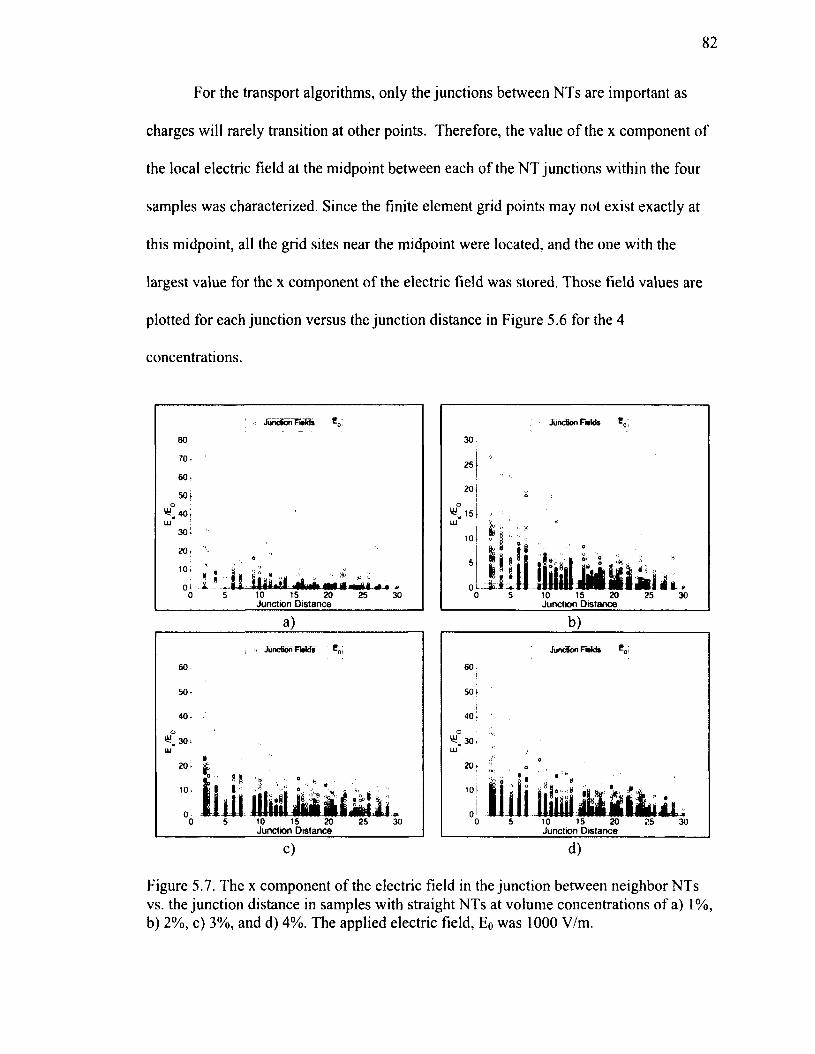
82
For the transport algorithms, only the junctions between NTs are important as
charges will rarely transition at other points. Therefore, the value of the x component of
the local electric field at the midpoint between each of the NT junctions within the four
samples was characterized. Since the finite element grid points may not exist exactly at
this midpoint, all the grid sites near the midpoint were located, and the one with the
largest value for the x component of the electric field was stored. Those field values are
plotted for each junction versus the junction distance in Figure 5.6 for the 4
concentrations.
■i Junction FMds
70.
2 0 .
a n ii *»Junction Distance
a)
. JuncSon FWds ^>i
60
50-
40 *
*Cao>LU
I20 ► £
E1°. E
' H
S 10 , H '
„ | r | j i s's>*i >
o - Jfc0 5 10 15 20 25
Junction Distance
J *30
JuocSonFWs *0;
30
25
20
< 1 5 ■Ui
fc i10
5
0 ll imlMililiii:if itltlil an U u M u10 15 20 25 30Junction Distance
b)JuncSon Fields
60;
50 j
40 [
ttCsoiLU
20 ►
10 Lo iiiJi0 5 10 15 20 25 30
Junction Distance
c) d)
Figure 5.7. The x component of the electric field in the junction between neighbor NTs vs. the junction distance in samples with straight NTs at volume concentrations of a) 1%,b) 2%, c) 3%, and d) 4%. The applied electric field, Eo was 1000 V/m.

83
From Figure 5.7, the reader might notice that there are set junction distances
within the sample. The pixilation method used for many of these studies generates NTs
along a three dimensional grid, therefore neighboring NTs will be set distances apart
from each other, with those distances corresponding to the size of the grid boxes, which
correspond to the diameter o f the NTs. In order to show how these set distances can arise,
Figure 5.8 shows a two dimensional slice through two parallel segments in NTs with
diameters of 5 A. In a sample such as these where the grid element size was set to this
diameter, the minimum distance is shown by the red arrow to be equal to ^ V2 — 2.5 j x
2, or 2.0711.
V A
5
5
y 2 .5\ -------------»
J
Figure 5.8. Simple representation of how one of the shortest distances can arise in the sample.
A distance o f 3.66 comes from two NT end caps occupying two three dimensional
cubes diagonally from each other. The distance through the diagonal of a cube with sides
of length 5 A is approximately equal to 8.66 (red dashed line in Figure 5.9). Therefore,

84
the length o f the solid red double arrow, which is the closest distance o f approach
between the two end caps is approximately 8.66 — 2 xradius, which is equal to 8.66 —
2x2.5, leading to a length o f 3.66 A.
Figure 5.9. Visual representation of how the junction distance of 3.66 can arise within samples. The two solid blue dots represent the two endpoints o f two neighboring NTs. Each endpoint is capped with a semi-sphere. The two endpoints would exist in the cubic lattice as diagonal to each other.
It can be seen from Figure 5.7 that many of the junctions have local fields near or
even below the value of the applied electric field. Flowever, it can also be seen that the
majority of the largest values for the x components of the local electric fields exist where
the junction distances are smaller.
Figure 5.10 shows the binned values of the x components of the electric fields in
junctions with the four smallest distances within the 0.04 concentration sample studied in
COMSOL. A distance of 5 A was the largest junction distance characterized in this study,
as transport through junctions larger than 5 A, will be very improbable. The exponential

85
term for tunneling in Eq. (2.2) will be approximately equal to 0.0025 at this distance.
Electric field values at the shortest distances were also examined more closely due to the
propensity of the electric field to have larger field values within the smaller junctions, as
seen previously in Figure 5.7.
I Junction Distance of 2.0711
40 60
E/ E0a)
10■Junction Distance of 3.6603
15 20
I Junction Distance of 2.5
1 I I I30 40
I Junction Distance of 5
30 40
C) d)
Figure 5.10. The distributions of the x component of the local electric fields between junctions at the four shortest possible distances between NTs. The specified junction distances are in A.
In order to attempt to capture the overall distribution in local electric fields
between junctions, the distributions from all four distances in Figure 5.10 were
combined. A Gaussian and Weibull distribution were both fit to the combined data using
the Matlab Curve Fitting Toolbox (Figure 5.11). This was done in order to be able to find

86
a simple representation of the distribution of local fields so that transport simulations
could incorporate these distributions to study the effects of the local field variations.
009* D istribution
— G au ss ian Fit008
0 07
006
0 05
004
0 03
0 02
0 01
00 10 20 30 40 50
« ju n c tio n 0
a)
008
006u.
004
0 02
« ju n c tio n D
b)
Figure 5.11. A a) Gaussian and b) Weibull distribution fit to the distribution of local fields in the junctions between neighboring NTs.
The Weibull distribution in Figure 5.11b was chosen as a simple representation of
the distribution of fields within junctions due to the tail end o f the Weibull fit enveloping

87
more of the larger electric field values than the Gaussian fit. This would then create a sort
o f worst-case scenario of the spread of local field values in transport simulations.
Matlab’s Curve Fitting Toolbox fits the simulation data to a general Weibull
distribution shown in Eq. (5.12).
In terms of general Weibull distributions, the constant b is the shape parameter of the
distribution, and the general scale parameter, A, for a Weibull distribution is given
A for this distribution would be equal to approximately 8.105. The expectation value for a
Weibull distribution is given by Eq. (5.13).
Where here T is the gamma function. This leads to an expectation value of approximately
1.799&Eo for this distribution.
Simulations were run with local electric field values chosen according to the
Weibull distribution in Figure 5.11 by using the inverse transform method.[134] In
Matlab, a uniform random number, u, is sorted between 0 and 1, which is then is
transformed into the variable, X with a target distribution. This is done by equating the
cumulative distribution of the target function to the uniform random variable, as in Eq.
f i x ) = a b x h xe axb (5.12)
by (V a) 1 ■ The Matlab fit led to values of 1.109 for b, and 0.09822 for a, meaning that
(5.13)
(5.14).
u = F(X) = 1 - e ~ ©m b
(5.14)
Inverting the equation then solves for X in terms of u.
1X = A (-log (1 — u)b (5.15)

88
Within these simulations, the local field would be determined by multiplying X by the
applied electric field. In order to ensure that the local fields within junctions were varied
as desired, carriers were then run through a test sample where the local electric fields
varied according to the Weibull distribution. Each time a charge attempted to move to
neighboring NTs, the value chosen for the electric field in each junction between
neighbor NTs was calculated according to the Weibull distribution and then stored. The
distribution of local electric fields from the test simulation is shown in Figure 5.12, and
indeed indicates that the values followed the target Weibull distribution.
* 10 '
•o
x-junction 0
Figure 5.12. The distribution of values for the x component of the local electric fields within each junction classified for the charge transport routine.
Once the correct implementation was assured, three separate simulations were
performed on samples that contained wavy NTs and a high aspect ratio. In the first, the
field within the junctions was considered a constant and equal to the applied electric
field. In the second, the local fields were varied according to Eq. (5.15), while in the third

89
the local fields were kept constant, equal to the expectation value of the distribution,
which is given by Eq. (5.13). The NTs were 225 nm in length and with a radius of 0.5 nm
in samples with dimensions that were 1 x 0.2 x 0.2 pm3. For these simulations the latest
version of the hopping algorithm, as described in Section 4.4, was used. The conductivity
values of these simulations are shown in Figure 5.13.
1.00E-01
E 1.00E-02 4u 4I/) 1.00E-03 £ 0>~
*->
■>4-1u
1.00E-04$O
Oo
O Applied E3TJCo
1.00E-05 O Weibull Dist.u 1.00E-06 & A E[X] Weibull
1.00E-07 O
0 0.002 0.004 0.006 0.008
NT Volume Concentration
Figure 5.13. Conductivity results for varying the electric fields within samples using version 2 of the transport routine.
The conductivity is slightly larger for the cases where the electric fields in the
junctions are set according to the Weibull distribution or the expectation value of that
distribution than in the case where the applied electric field is used. This indicates that
although using the applied field as the field in the junction leads to an under prediction of
the conductivity, the use of a constant electric field is a reasonable approximation, if the
mean value of the electric field distribution is used. From these results, it can be seen
that results obtained throughout this dissertation may not correspond to what would be
expected at the electric field chosen for those simulations. However, they are expected to

90
correspond to a case with a smaller electric field, which from the case studied here can be
expected to be about 8 times smaller. Thus far, this section has focused on the x
component of the electric field. This is because in many of the studies within this work, it
was assumed that the local fields within the junctions between neighboring NTs would on
average be dominated by the electric field along the x direction. However, it was of
interest to study the behavior o f the y and z components of the local electric fields within
junctions to check this assumption. Figure 5.14a and b show the distributions of y and z
components of the electric field within the junctions, respectively, within the 0.04 volume
concentration sample. This concentration was chosen as it had an acceptable number of
NT-NT junctions.
I Distribution I Distribution
junction 0 'junc tion 0
a) b)
Figure 5.14. The distribution of the average values of the a) y component and b) z component o f the fields within the junctions between neighboring NTs.
It is clear that the polarization of the conductive inserts will generate y and z
components of the electric field. However, the distribution is centered and peaked about
zero, indicating that these components on average will be zero. In order to see how these
induced polarizations may affect the local electric fields within the junctions, the total

91
value of the electric field at the midpoint o f each NT-NT junction is characterized for all
four concentrations. Figure 5.15 shows a scatter plot of the local norm of the electric field
at the midpoint of each junction versus the distances of the junctions.
Junction Fields— E0
100
OUJN,
§CC3
UJ
2010 300Junction Distance
a)
Junction Fields — E0j
60:
10 20 Junction Distance
b)
Junction Fields
Junction Distance
Junction Fields
Junction Distance
c) d)
Figure 5.15. The norm of the electric field at the midpoint in each junction versus the junction distances for concentrations of a) 0.01, b) 0.02, c) 0.03, and d) 0.04.
As with the x components, there are locations within junctions where the local
field is larger than Eo, with the larger values tending to exist in the shorter junctions.
Thus, the distributions o f the total value of the electric field for the four shortest junction
distances in the 0.04 volume concentration sample are shown in Figure 5.16.

92
■Junction Distance of 2.0711
■ 1 M i20 40 60
E /E . n o rm 0
80 100
a)
Junction Distance of 3.6603
30 40E /E .n o rm 0
Junction Distance of 2.5
II I I40 60
E / E .n o rm 0
b)
|M Junction Distance of 5j
40 60
“ n o r n / ^ 0
c) d)
Figure 5.16. The distributions of the local electric field norm between junctions at the four shortest possible distances between NTs.
These four distributions were then combined and fit to a Weibull distribution
(Figure 5.17), as they were in the case of the x component of the electric field. The fit
was a least squares fit performed in the Matlab Curve Fitting Toolbox using the least
absolute residual method.

93
Junction Field Distribution — Weibull Fit
0.08
0.04
0.02
norm 0
Figure 5.17. Weibull fit to the combined distributions o f the local electric field norms for the 4 shortest junction distances in the 0.04 volume concentration case.
For this fit, the parameters, a and b, in Eq. (43) were 0.04852 and 1.443,
respectively. The R-square for this fit was 0.9961. This compares to values of 1.109 for b
and 0.09822 for a in the general Weibull distribution found for the x component of the
electric fields within junctions. The Wiebull distributions found in Figure 5.11 and Figure
5.17 are shown together in Figure 5.18 to compare the distribution of the local norm of
the electric field to the distribution of the x component of the electric field. It can be seen
that the Weibull distributions are actually quite similar, indicating that overall, the y and z
components o f the local electric field will not significantly alter the value of the electric
field within the junctions, and the x component of the junction should be sufficient to
describe charge transport within each junction. However, in the interests of complete
understanding, future works are planned to incorporate these induced polarizations in the
y and z directions.

94
— WeibUrt-X - - WeibulkNorm0.09
0.08
0.07
0.06
0.05
0.04
0.03
0.02
0.01
100
Figure 5.18. The Weibull distributions for the x component and norm of the electric field in the midpoints of the junctions for the four shortest distances in the 0.04 concentration sample.
5.2 Comparison to Experiments with the Improved Transport Routine
Once the model was altered, as described in Section 4.4, and the behavior of the
local electric fields within NT-NT junctions was better understood, it was again of
interest to see how well the model matched up with experimental values when the
parameters within the model were solved for using first principles. Simulations were run
with the improved charge transport routine on samples that were 1 x0.2x0.2 pm3 in length
with an applied electric field of 10 V/cm. The results were then compared to the same
experimental results on PAN/CNT composites used in Section 4.4, shown in Figure 5.19.
The extrapolation of the results was performed by again fitting simulation results to the
power law for conductivity, Eq. (1.1).

95
1CT
10
* 10 Ic
10 •6
« Simulation Data Extrapolation
o Experimental
10-8
10 -100.05 0.1
Cone0.15 0.2
Figure 5.19. Comparison to experimental results from Guo et al. [125] and Pradhan et a/.[120]with results under an applied electric field of 10 V/cm.
This version of the model also sees excellent agreement with the experimental
results. This is significant as this version o f the model is based solely on the physics of
the system, with no fitting parameters to be used for the simulation. Now it does need to
be noted that with the original version of the model, the applied electric field was set
equal to 1 V/cm in the simulations in section 4.4, not 10 V/cm as in this case with the
improved version of the model.
To begin to explain this, this author must note that in the simulation with the
improved model, the electric field within the junctions was set to be the expectation value
of the distribution of the electric fields within junctions (see Section 5.1). This
expectation value was around 8 times the applied electric field. It should be remembered
from Section 4.2 that v0 is calculated such that it is proportional to the junction electric
field in the improved version of the model. This means v0, for an applied field of 10
V/cm, would have been 8.54x10⁶ s '1, leading to a minimum hopping time of 1.17x10'7 s.

In the comparison using the original routines, the value for v0 was found to be around
0.8x10⁴ s '1, which would give a minimum time for a hop that was equal to 1.25x1 O’4 s.
The difference in the time scale for hops using the two versions can be explained by the
fact that in the original version, the charge was assumed to travel down the NTs without
taking any time. The improved model adds the time for the charge to move through the
NT, but also added a larger time penalty for hops when the charge moves through a NT
against the force of the electric field (see Section 4.4). Therefore, the time scale for hops
within this improved version of the model should be smaller to account for this.
In the experimental studies on PAN/CNT composites, used for comparisons
within this work, it is not reported what the voltage was that was used for measuring the
conductivity of these composites. Rather, the experimental studies used here for
comparison are more concerned with conductivity at and around the critical concentration
and the factors leading to the observed increase in conductivity.[120], [125] In fact, many
o f the experimental works with CNT composites are similar in that the voltages, and
therefore the electric field, used to study DC conductivity are not usually reported. It is
therefore unknown what the applied electric field was in these experimental studies. This
can be problematic as changes in the voltage can lead to differences in electrical
properties o f these materials, and make it difficult to compare to experimental results.
5.3 Effect of the Applied Electric Field on Conductivity
In Section 5.1, it was determined that the distributions of the local electric fields
within junctions do not have significant impacts on charge transport, within the
framework of Eq. (3.12) where v0 was made dependent of the electric field. It was
therefore of interest to see how changing the applied electric field on samples affects

charge transport within these simulations. Samples that were 1 x 0.2 x 0.2 p,m3 in
dimensions with NTs having a maximum length of 200 nm with a radius of 0.5 nm were
simulated with an applied electric field of 1 V/cm, 10 V/cm, and 100 V/cm. The local
fields within junctions were assumed to be the average of the distribution of the local
fields, which was around 8 times the applied field (see Section 5.1). Figure 5.20 shows
the conductivity for the samples under the 3 different applied electric fields.
1.00E-01
E 1.00E-02 Au A □LO> 1.00E-03 A
□0
O’>tJ
1.00E-04 I_1o o
A 100 V/cmD"Oc 1.00E-05□ □ 10 V/cmou 1.00E-06 A O 1 V/cm
1.00E-070 0.002 0.004 0.006 0.008
NT Volume Concentration
Figure 5.20. Conductivity results for varying the applied electric field.
It can be seen that by increasing the electric field applied to the sample the
conductivity of the samples increases. A larger electric field will give more energy to a
charge moving down a conductor, or a NT in these simulations, which in turn effectively
lowers the tunneling barrier between two neighboring NTs. This is captured within this
model as the probability for downfield hops between neighboring NTs increases with
increasing electric field, therefore decreasing the probability for a backwards hop to
occur. This same effect has also been seen within other models that incorporate tunneling
into their model. In the theoretical work done by Bao et al., a decrease in the tunneling

98
barrier height between neighboring NTs also led to a decrease in conductivity within
composite samples.[95] In addition, v0 in Eq. (3.12) is calculated such that it is
proportional to the electric field within the junction. Therefore, increasing the electric
field will increase v0, which then will decrease the transport time for hops. With this in
mind, a further look at the calculation o f v0 for specific samples is needed and discussed
in the future plans section of this work.

CHAPTER 6
CONCLUSIONS
A stochastic approach has been taken to model charge transport properties in CNT
composite materials. Simulation boxes as large as 1 pm long have been modeled with
over 5000 NTs that were 0.5 nm in diameter and up to 225 nm long (1:450 aspect ratio).
This shows the capability of the model to study samples that can be directly compared to
experiments while keeping a nanoscopic resolution on its physical properties. The results
presented in this work see quantitative agreement with experimental works, and
predictions from the model are qualitatively sound on the relationship between various
aspects of geometries and conductivity.
When it comes to practical aspects of the simulations, it is determined that the
simulation box needs to be 4 to 5 times longer than the NTs for the diversity in topology
to be enough to mask size effects. Above this size, carriers will sample a configuration
that is diverse enough to ensure that increasing the size further does not significantly alter
results. The progress towards a more diversified sample is observed to be smoother for
samples with NTs with a larger aspect ratio. Finally, notice that by simply re-scaling
some parameters such as the tunneling constant, these simulations can be scaled up to
larger sizes.
Qualitatively, results from the model show an excellent agreement with the
percolation behavior expected for these samples. The model also predicts the correct
99

100
relationship with NT waviness and aspect ratio that are here explained from the structural
features at the nanoscale. Indeed, as the junction resistance is the limiting factor, low
aspect ratios or high waviness will lead to more NT-NT junctions between electrodes,
decreasing conductivity. Theoretical percolation does not account for the junction
resistance and transport in a percolated network will be insensitive to aspect ratio or
waviness. Conductivity is found to be more sensitive to aspect ratio than waviness,
although waviness does affect conductivity.
Simulations have been performed to understand how agglomeration impacts
charge transport within nanocomposite materials. Results indicate that heavy
agglomeration is indeed detrimental to charge transport in these materials. However, it
has been shown that for optimal charge transport, especially at low concentrations, the
formation of agglomerates actually improved transport. Interconnected bundles of NTs
connected to each other by NTs that stick out like hairs from each agglomerate allow for
better charge transport than both randomly dispersed NTs and large bundles of NTs that
are poorly interconnected. This is due to more efficient distribution of conduction paths
that leaves voids in the sample in favor to more densely packed groups of NTs that
connect the electrodes. The effect will be almost imperceptible above percolation and
will have a larger impact at the onset of percolation and at the threshold. In fact, some
agglomeration leads to a lower percolation threshold. Looking in more detail, it is
observed that as concentration grows into early percolation, more uniform samples do
lead to a larger number of carriers reaching the collection electrode, but with a lower
mobility. At these relatively larger concentrations, pathways exist at almost all degrees
of agglomeration. However, for a more uniform distribution, the number of paths is larger

101
than for the percolated samples and thus more carriers reach the collection electrode.
Nonetheless, the average distance between NT’s is also larger in those uniform samples,
explaining the lower mobility.
It is evident from this work that the local electric field within composites will not
be equal to the applied electric field. In fact, there will be hotspots within these
composites where the local electric field is significantly larger than the applied electric
field. It has also been shown that there are points within junctions between NTs where the
electric field is actually lower than the applied electric field. This work has shown that
the distributions of local electric fields within composites with a conductive filler and
insulating matrix will have minimal effects on charge transport routines within these
materials. Thus, assigning the same electric field value to all the junctions would produce
very similar results compared to assigning valued based on a distribution, provided that
the value assigned is the mean value of the distribution o f electric fields. It does remain a
fact however that the local electric fields within composite materials will not necessarily
equal the applied electric field and this must always be kept in consideration.

CHAPTER 7
RELATED AND FUTURE WORKS
7.1 Further Improving this Model
While this model does indeed capture many qualities o f charge transport within
CNT composites, there are a few characteristics o f the model that need to be studied
further. Improvements have been made in attempts to characterize systems from first
principles using the fundamental physics of the system. In an attempt to do this, v0 has
been changed from a fitting parameter, to a parameter that is based on Ohm’s law and
DFT calculations. A further study into the validity o f this change needs to be performed.
First, v0 has been made to be proportional to the electric field within the junction between
NTs, which may or may not be an appropriate value. As has been presented in Section
5.1, the local fields within a composite sample do vary due to the propensity of the
conductive inclusions to polarize within the insulating matrix. If v0 is to be continued to
be calculated in this way, then a possible improvement may be to calculate the voltage
differential between neighboring CNTs. In this way, the voltage drop between
neighboring CNTs, and therefore the voltage drop across the junction resistances can be
known and applied to the calculation of v0. This type of study can be performed in
Comsol as were the studies presented in Section 5.1, and could potentially show that the
local voltage drops do indeed vary widely within the material.
102
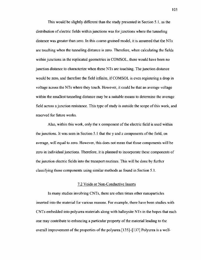
103
This would be slightly different than the study presented in Section 5.1, as the
distribution of electric fields within junctions was for junctions where the tunneling
distance was greater than zero. In this coarse-grained model, it is assumed that the NTs
are touching when the tunneling distance is zero. Therefore, when calculating the fields
within junctions in the replicated geometries in COMSOL, there would have been no
junction distance to characterize when these NTs are touching. The junction distance
would be zero, and therefore the field infinite, if COMSOL is even registering a drop in
voltage across the NTs where they touch. However, it could be that an average voltage
within the smallest tunneling distance may be a suitable means to determine the average
field across a junction resistance. This type of study is outside the scope of this work, and
reserved for future works.
Also, within this work, only the x component of the electric field is used within
the junctions. It was seen in Section 5.1 that the y and z components of the field, on
average, will equal to zero. However, this does not mean that those components will be
zero in individual junctions. Therefore, it is planned to incorporate these components of
the junction electric fields into the transport routines. This will be done by further
classifying those components using similar methods as found in Section 5.1.
7.2 Voids or Non-Conductive Inserts
In many studies involving CNTs, there are often times other nanoparticles
inserted into the material for various reasons. For example, there have been studies with
CNTs embedded into polyurea materials along with halloysite NTs in the hopes that each
one may contribute to enhancing a particular property of the material leading to the
overall improvement of the properties of the polyurea.[ 135]—[ 137] Polyurea is a well-

104
known and versatile material that is used for various coatings, containers, structures, and
components due to their chemical and mechanical durability.
In light of this, it was determined that the model needed the capability to consider
voids within the sample in order to simulate a non-conducting nano-insert. Not only
would it be useful if the desired composite contains multiple types o f NTs, but also in the
event that the specific polymer has a specific geometry that does not allow the nano
inserts to occupy a certain space. In the above-mentioned example o f polyurea, the
polyurea, upon the mixture of the two precursor components, will form soft regions and
hard crystalline regions. In the event one wanted to simulate a geometry where the nano
inserts were only dispersed within the soft region, this type of generation would be
useful.
In the current implementation, two types of voids can be created, cylindrical or
spherical. Cylindrical voids are created by considering a straight line between two
random points within the sample and then giving a cylindrical volume where those two
points are connected, with semispherical end caps on the ends. In the case a spherical
void is desired, these two points in space could just simply be created in consecutive grid
points. As in the other generation methods, it is ensured that these new nanoinserts do not
intersect with each other so that accurate volume concentrations are reached. Once these
nanoinserts have been generated within a sample, the NTs are placed around them, as
previously discussed. Samples with different volume percentages of the second type of
nanoinsert are shown in Figure 7.1. The normal NTs are shown in green while the second
NTs are shown as voids in the sample. For this simple visualization, the CNTs were 0.5
nm in diameter and 30 nm in length while the voids were 3 nm in radius and 20 nm long.
105
Samples were 100x30x30 nm3 in dimension. The NTs were kept at a constant volume
fraction of 0.04.
b)
Figure 7.1. Samples with a second type of insert, shown here as voids, for volume concentrations of a) 0.00 and b) 0.05. The volume concentration of the normal NTs (in green) was kept constant.
Clearly there is an increase in the amount of white space (voids) as the volume
concentration of the second type o f nanoinsert is increased. This type of generation adds
to the versatility of the types of materials that can be studied.
7.3 Further Characterization of Various Composites
Further work can be done within this model to classify other composite materials.
It is planned that continued work will be done in conjunction with the Air Force Research
Laboratories and associated collaborators to classify not only CNT composites, but other
composites with other various conductive nanoinserts and various polymers. The model
is at a point that any polymer material can be classified for tunneling properties and
employed within this model. Materials with nonconductive inserts can also be studied
within this model through the use of the portion of the routine that creates voids within
106
the samples. These voids can also be modeled as a second type of insert that has different
conductive properties, whether insulated or semiconducting.
In addition, the current NTs within the samples here are all considered metallic.
However, the model can be parameterized to more appropriately represent CNT
composites by making a portion of the NTs semiconducting in nature. Generally
speaking, 2/3 of the possible ways that a sheet of graphene can be rolled, or the chirality
o f the CNT, will lead to semiconducting CNTs for single-walled CNTs. The remaining
1/3 will be metallic. In addition, large diameter single-walled CNTs and many multi
walled CNTs tend to be metallic in nature.
A metallic CNT will have a relatively small gap between the valence and
conduction states, and therefore it can be approximated that a charge at the Fermi level
can easily be promoted into the conduction band of the CNT. However, semiconducting
NTs will have an energy gap between the valence and conduction states, and therefore
any charge attempting to move to or through a semiconducting NT will have to receive
some amount of energy to promote charges into the conduction state. The inclusion of
semiconducting NTs can lead to three new situations within the transport routine: 1) A
charge attempting to move from a metallic CNT to a semiconducting CNT, 2) A charge
attempting to move from a semiconducting CNT to another semiconducting CNT, or 3) A
charge moving from a semiconducting CNT to a metallic CNT. In case one, the charge
moving in the metallic CNT attempting to transition to a semiconducting CNT will have
to overcome the energy in the gap between the Fermi level of the metallic CNT and the
conduction state in the semiconducting CNT. In case 2, the charge attempting to move
between two semiconducting CNTs will move from the conduction state in the first CNT

107
to the conduction state in the second CNT. In case 3, the charge will have to move from
the conduction level in the semiconducting CNT to the Fermi level of the metallic CNT.
The exact references for the Fermi level in each CNT and the relative gaps between
conduction and valence states in semiconducting CNTs will need to be known to
incorporate these into the transport routine.
7.4 Effects of Structural Changes on Charge Transport
7.4.1 Cracks in Samples
Simple simulations were performed in order to study how changes in the
morphology of a CNT composite material might affect charge transport through these
materials. One of the major structural defects that can occur in many materials under
various loading amounts is micro cracking. In order to structurally monitor one such
instances of damage, the structure to be monitored could be a nanocomposite itself or a
nancomposite coating can be applied to the structure. If structural changes relate to
changes in conductivity, then those changes in conductivity can be used to sense changes
in the structure, particularly cracks. In order to accomplish this, a short routine was
created that takes a previously generated sample, and incrementally cracks the sample
from bottom-to-top in a user-specified number of different sections. In the first cracking
step, the bottom section was spread apart a specified amount. In the second cracking step
the bottom section was spread apart once again the same amount, while the next section
above was also cracked. In this way, a crack begins at the bottom of the sample, and
grows upwards towards the top of the sample. Figure 7.2 shows a sample, containing 6%
volume NTs, cracking in various stages where each cracking step spreads the bottom

108
section of the sample by 0.5 A. Figure 7.3 shows the number of charges, out of 1000, that
are collected at the opposite electrode for each of the cracking steps.
Figure 7.2. A simple crack forming through the middle of a virtual nanocomposite sample.
700
600
500
400
300
200
100
Cracking Step
Figure 7.3. The number o f charges, out of 1000, that reach the opposite electrode at each cracking step.
Clearly there is a drop in the number of charges that are able to reach the opposite
electrode as the crack develops through the middle of the sample. However, the

109
maximum width for the crack at step fourteen was 7 A at the bottom of the sample,
tapering towards the top of the sample. This crack width is still small enough that some
charges are still able to reach the opposite end of the sample. So charge transport is
inhibited somewhat, but not fully stopped. In fact, most charges travel through a path that
runs through the top of the sample, as is illustrated in Figure 7.4, where the path o f one
charge is shown running through the top of the sample. The color, blue to red, represents
the time, early or later, in the transport that each NT was visited by the charge.
Figure 7.4. The path taken by one charge, highlighting the visited NTs.
It was of interest to see the type of crack that would be needed to cause a more
drastic change in charge transport through these samples. In order to accomplish this,
another crack was induced in a sample containing a larger volume percentage, 8%, of
NTs to ensure a quality conductive sample before cracking. In this sample, the crack
again began at the bottom section, with the sections being spread by 2 A at each step. The
final crack is shown Figure 7.5 and compared to the thinner crack from the 6% volume
sample, which was taken from Figure 7.2.

110
a) b)
Figure 7.5. a) The thinner crack from the 6% volume NT sample and b) The wider crack in the 8% volume NT sample.
Figure 7.6 shows the number of charges, again out of 1000, that reach the
opposite electrode in both these cracked samples. There is a drastic drop in the number of
charges that reach the opposite electrode for the sample with the much larger crack. The
tunneling parameter for these two samples was 0.6 A'1, the value calculated for PAN. At
the tenth crack step, the top sections of the samples begin their first separation of 0.5 A
and 2 A for the small and large cracks respectively. In the 8% volume NT sample with
the large crack, it is at this point, the tenth crack step, that the steep decline in charges
reaching the opposite electrode begins to occur. So, for this material, if a crack begins to
form that is any greater than 2 A throughout the sample, charge transport will begin to be
inhibited by the crack. If the electrical conductivity of this material is constantly
monitored in the correct way, the formation of cracks could be detected even before they
are visible without the use of advanced microscopes.

1000 ; —♦ “ 6% Vol. Smallai
TJoi—Crack
800-* -8 % Vol. Large
Crack" ^ 600
1 1 400f0 OJ
5 =5 200 u
0 5 10 15Crack Step
Figure 7.6. The number of charges that reach the opposite electrode for the 6% volume sample (with a thinner crack) and 8% volume sample (with the thicker crack).
Now the above work is detailed on a very simple crack forming through the
middle o f the sample. This very preliminary work shows that the model can show that if
there is a crack through the sample, the conductivity of the sample will be lowered, and
should be able to be sensed by monitoring the electrical response of the material.
However, a more accurate prediction of a crack forming through the sample is needed for
this application of the model to continue. What would be most advantageous would be to
take into account the structural and mechanical properties of the composite, either
through experimental or modeling approaches, so that an understanding o f how the
material would crack could be determined. If the structural damage or deformation of the
composite could be predicted, then the electrical response of the material during and after
the formation of the crack could also be predicted. More detailed study and work is
required for this application of the model to reach its full potential.
7.4.2 Effect of Compression on Charge Transport
Another type of structural change that occurs frequently in these types of
materials is that of compression or stretching due to external forces. Simple compression

12
algorithms have been developed to compress virtual samples from all directions towards
the center o f the sample. No mechanical properties of the underlying polymer or CNTs
within the sample have been taken into account. The CNTs were simply pushed closer
towards the center of the sample, however, the point to which the CNTs were being
compressed can be altered by the user. Figure 7.7 shows how samples could be
compressed.
Figure 7.7. Compression of samples towards the center o f the sample. Increasing compression from left to right.
Clearly the volume concentration of the CNTs increases as the sample shrinks.
Figure 7.8 shows the percentage of injected charges reaching the collection electrode at
various compression steps.
ifis
9 cu
0.6
0.4
02
00 2 4 6
CNT Volume Concentration (%)
Figure 7.8. Percentage of charges reaching the collection electrode as the sample is compressed.
113
The model already has the capability to predict conductive properties of samples,
and to compress samples. The main task for this portion of the model to have a greater
impact in future studies is for the mechanical properties of each material to be taken into
account in the compression routines. As of right now, the NTs in the samples are moved
arbitrarily, when in reality the compression of the sample and the movement of the filler
is going to be dependent on the mechanical properties of both the filler and the polymer.
7.4.3 Vibrational Studies with Charge Transport
Another possible future work that can be performed with this model is to study
the effects of vibrations in these materials. The idea behind this work would be to
monitor materials through changes in electrical resistance of nanocomposite coatings. If
one could monitor the vibrational frequencies of the underlying material through
electrical resistance measurements, any change in the vibrational frequencies of the
composite itself or the underlying material would indicate either a change has occurred in
the material, or some event has occurred to the material.
The method for pursuing this study would be to induce vibrations within the
material, and then monitor charge transport characteristics versus various types of
vibrations and various frequencies. The way this would be implemented into the current
model is to track at what time the charge reaches a particular NT. As the user is the one
determining the vibrational pattern, or the equations governing the vibrational motion of
the material, the change in position of the material can be known at that time and
incorporated into the transport routines.
Through studies such as this, the conductivity of samples for various types of
vibrations, such as normal modes, or say a compression wave through the sample, may be

114
known. If for example, a compressive shock wave propagates through the material, and
the conductivity profile for such a wave is known, one can easily monitor such an even
occurring.
For this work to progress, one must take into account the micro and nano-scale
mechanics in the composite. The exact interactions of the material may need to be taken
into account. The underlying normal modes of various composites will also need to be
known.
7.5 Polymer Hydrogel Simulations
Recently there has been much study on polymer hydrogels and their use in
controlled drug delivery. Hydrogels are polymer materials that swell in the presence of
water and have been widely used in various materials ranging from contact lenses to
absorbent materials in diapers. The main premise behind these hydrogels is that they
could behave as smart materials for controlled drug delivery due to their propensity to
swell when water is introduced to the polymer. They then will shrink back once the water
has been removed. The drug to be delivered can be loaded into a swollen hydrogel, which
can be then be dehydrated, leaving only the drug in the shrunken hydrogel material.
These materials have been widely studied both experimentally and theoretically and
swelling rates have been established. However, modeling of these materials can allow
further understanding of the nature o f the swelling hydrogel depending on the type of
hydrogel.
A portion of the model developed in this dissertation has been used in preliminary
studies of polymer hydrogels for drug delivery in order to simulate the release of various
drug molecules in Monte Carlo dynamics simulations. The first task to simulate these

115
processes is to generate samples that resemble hydrogels in geometry. The generation
routine discussed in Section 2.1 has been altered slightly so that polymer strands are
represented by connected cylindrical segments, as were the NTs. However, these coarse
grain polymer strands are allowed to overlap with each other to more accurately represent
the physical and chemical crosslinking that occurs in these hydrogels. This crosslinking
creates a matrix type structure in these hydrogel materials, which is one of the main
reasons why they can swell and shrink.[ 138] The generation routine can be easily adapted
for the physical crosslinking o f the polymer strands. However, for chemical crosslinking
o f the polymer, any point at which two strands crosslink must remain attached to each
other, and will be a major factor in determining how the polymer hydrogel swells and/or
shrinks.
In addition, the routine has been adapted so that drug molecules can be added
within the polymer hydrogel matrix, or outside the matrix. Each molecule is also a coarse
grain approximation as a simple sphere, or as a straight cylinder depending on the drug
molecule being studied. In the preliminary Monte Carlo dynamics simulations, the same
neighbor-checking algorithm that has been used to find the nearest NT neighbors as in
Section 2.2 has been employed in order to calculate the distance between polymer strands
and drug molecules. A sample is shown in Figure 7.9.

Figure 7.9. Hydrogel sample. The green segments are the polymer strands, and the red spots are the drug molecules in the sample.
The ability to use these routines and algorithms has led to an efficient means to
begin the process of studying and modeling these materials. Further work to continue
studying drug delivery with hydrogels is needed. The physical interactions between
polymer strands and drug molecules will need to be calculated and included into the
dynamics simulations. Previous works have studied drug delivery using halloysites, a
naturally occurring clay NT, and many of the underlying physical equations used in that
study could be applied to the dynamics simulations for drug delivery in hydrogel systems
in a synergistic interaction with this work.[139]

BIBLIOGRAPHY
[1] S. Iijima, “Helical microtubules of graphitic carbon," Nature, vol. 354, no. 6348, pp. 56-58, 1991.
[2] M .S. Dresselhaus, G. Dresselhaus, and R. Saito, “Physics of carbon nanotubes,” Carbon N. Y., vol. 33, no. 7, pp. 883-891, Jan. 1995.
[3] T. W. Ebbesen, “Carbon nanotubes,” Phys. Today, vol. 49, no. 6, pp. 26-32, 1996.
[4] V. Popov, “Carbon nanotubes: properties and application,” Mater. Sci. Eng. R Reports, vol. 43, no. 3, pp. 61-102, Jan. 2004.
[5] P. R. Bandaru, “Electrical properties and applications o f carbon nanotube structures,” J. Nanosci. Nanotechnol., vol. 7, no. 3, pp. 1239-1267, Apr. 2007.
[6] J. Moore, J. Dutta, H. F. Tibbals, and G. L. Homyak, Introduction to Nanoscience and Nanotechnology. CRC Press, 2008.
[7] E. Brown, L. Hao, J. C. Gallop, and J. C. Macfarlane, “Ballistic thermal and electrical conductance measurements on individual multiwall carbon nanotubes,” Appl. Phys. Lett., vol. 87, no. 2, p. 023107, 2005.
[8] Z. Han and A. Fina, “Thermal conductivity of carbon nanotubes and their polymer nanocomposites: A review,” Prog. Polym. Sci., vol. 36, no. 7, pp. 914-944, Jul. 2 0 1 1 .
[9] Y. Ando, X. Zhao, and H. Shimoyama, “Physical properties of multiwalled carbon nanotubes,” Int. J. Inorg. Mater., vol. 1, no. 1, pp. 77-82, 1999.
[10] A. Thess, R. Lee, P. Nikolaev, H. Dai, P. Petit, J. Robert, C. Xu, Y. Lee, S. Kim, A. Rinzler, D. Colbert, G. Scuseria, D. Tomanek, J. Fischer, and R. Smalley, “Crystalline ropes of metallic carbon nanotubes,” Science, vol. 273, no. 5274, pp. 483-7, Jul. 1996.
[11] M. Treacy, T. Ebbesen, and J. Gibson, “Exceptionally high Young’s modulus observed for individual carbon nanotubes,” Lett, to Nat., vol. 381, no. 6584, pp. 678-680, 1996.
[12] S. Iijima, C. Brabec, A. Maiti, and J. Bemholc, “Structural flexibility of carbon nanotubes,” J.Chem.Phys., vol. 104, no. 5, pp. 2089-95, 1996.
117

118
[13] J. Li, Q. Zhang, D. Yang, and J. Tian, “Fabrication of carbon nanotube field effect transistors by AC dielectrophoresis method,” Carbon N. Y., vol. 42, no. 11, pp. 2263-2267,Jan. 2004.
[14] A. I. Zhbanov, N. I. Sinitsyn, and G. V. Torgashov, “Nanoelectronic devices based on carbon nanotubes,” Radiophys. Quantum Electron., vol. 47, pp. 435-453, 2004.
[15] M. M. Shulaker, J. Van Rethy, T. F. Wu, L. Suriyasena Liyanage, H. Wei, Z. Li,E. Pop, G. Gielen, H.-S. P. Wong, and S. Mitra, “Carbon nanotube circuit integration up to sub-20 nm channel lengths,” ACS Nano, vol. 8, no. 4, pp. 3434- 3443, Apr. 2014.
[16] M. Xia, Z. Cheng, J. Han, and S. Zhang, “Extremely stretchable all-carbon- nanotube transistor on flexible and transparent substrates,” Appl. Phys. Lett., vol. 105, no. 14, p. 143504, Oct. 2014.
[17] T. Abate, “A first: Stanford engineers build basic computer using carbon nanotubes,” Stanford Report, 2013. [Online]. Available: http://news.stanford.edu/news/2013/september/carbon-nanotube-computer- 092513.html.
[18] T. McNally, P. Potsehke, P. Hailey, M. Murphy, D. Martin, S. E. J. Bell, G. P. Brennan, D. Bein, P. Lemoine, and J. P. Quinn, “Polyethylene multiwalled carbon nanotube composites,” Polymer (Guild/)., vol. 46, no. 19, pp. 8222-8232, Sep.2005.
[19] W. Bauhofer and J. Z. Kovacs, “A review and analysis of electrical percolation in carbon nanotube polymer composites,” Compos. Sci. Techno!., vol. 69, no. 10, pp. 1-26, 2008.
[20] G. Rebord, N. Hansrisuk, B. Lindsay, C. Lekakou, G. T. Reed, and J. F. Watts, “Electrofunctional polymer nanocomposites,” 2008 2nd Electron. Svst. Technol. Conf, pp. 1401-1406, Sep. 2008.
[21] M. Moniruzzaman and K. I. Winey, “Polymer nanocomposites containing carbon nanotubes,” Macromolecules, vol. 39, no. 16, pp. 5194-5205, 2006.
[22] R. Simoes, J. Silva, R. Vaia, V. Sencadas, P. Costa, J. Gomes, and S. Lanceros- Mendez, “Low percolation transitions in carbon nanotube networks dispersed in a polymer matrix: dielectric properties, simulations and experiments.,” Nanotechnology, vol. 20, no. 3, p. 035703, Jan. 2009.
[23] M. Njugun, “Characterisation of multi wall carbon nanotube-polymer composites for strain sensing applications,” Queensland University of Technology, 2012.

119
[24] X. Wang, Q. Jiang, W. Xu, W. Cai, Y. Inoue, and Y. Zhu, “Effect of carbon nanotube length on thermal, electrical and mechanical properties of CNT/bismaleimide composites,” Carbon N. Y., vol. 53, no. March, pp. 145-152, Mar. 2013.
[25] N. Hu, Z. Masuda, C. Yan, G. Yamamoto, H. Fukunaga, and T. Hashida, “The electrical properties of polymer nanocomposites with carbon nanotube fillers,” Nanotechnology, vol. 19, no. 21, p. 215701, May 2008.
[26] E. Kemner, I. M. de Schepper, G. J. Kearley, and U. A. Jayasooriya, “The vibrational spectrum of solid ferrocene by inelastic neutron scattering,” J. Chem. Phys., vol. 112, no. 24, p. 10926, 2000.
[27] H. H. So, J. W. Cho, and N. G. Sahoo, “Effect of carbon nanotubes on mechanical and electrical properties o f polyimide/carbon nanotubes nanocomposites,” Eur. Polym. J., vol. 43, no. 9, pp. 3750-3756, Sep. 2007.
[28] Z. Ounaies, C. Park, K. Wise, E. Siochi, and J. Harrison, “Electrical properties of single wall carbon nanotube reinforced polyimide composites,” Compos. Sci. Technol., vol. 63, no. 11, pp. 1637-1646, Aug. 2003.
[29] C. Park, Z. Ounaies, and K. Watson, “Dispersion of single wall carbon nanotubes by in situ polymerization under sonication,” Chem. Phys. Lett., vol. 364, no. 3-4, p p .303-308, 2002.
[30] B. E. Kilbride, J. N. Coleman, J. Fraysse, P. Foumet, M. Cadek, A. Drury, S. Hutzler, S. Roth, and W. J. Blau, “Experimental observation of scaling laws for alternating current and direct current conductivity in polymer-carbon nanotube composite thin films,” J. Appl. Phys., vol. 92, no. 7, p. 4024, 2002.
[31] A. K. Kota, B. H. Cipriano, M. K. Duesterberg, A. L. Gershon, D. Powell, S. R. Raghavan, and H. A. Bruck, “Electrical and rheological percolation in polystyrene/MWCNT nanocomposites,” Macromolecules, vol. 40, no. 20, pp. 7400-7406, Oct. 2007.
[32] M. Lahelin, M. Annala, A. Nykanen, J. Ruokolainen, and J. Seppala, “In situ polymerized nanocomposites: Polystyrene/CNT and poly(methyl methacrylate)/CNT composites,” Compos. Sci. Technol., vol. 71, no. 6, pp. 900- 907, Apr. 2011.
[33] O. Regev, P. N. B. ElKati, J. Loos, and C. E. Koning, “Preparation of conductive nanotube-polymer composites using latex technology,” Adv. Mater., vol. 16, no. 3, pp. 248-251, Feb. 2004.
[34] M. H. Al-Saleh, H. K. Al-Anid, and Y. A. Hussain, “CNT/ABS nanocomposites by solution processing: Proper dispersion and selective localization for low percolation threshold,” Compos. Part A Appl. Sci. M anuf, vol. 46, pp. 53-59, Mar. 2013.

120
[35] E. Zapata-Solvas, D. Gomez-Garcia, and A. Dominguez-Rodriguez, “Towards physical properties tailoring of carbon nanotubes-reinforced ceramic matrix composites,” J. Eur. Ceram. Soc., vol. 32, no. 12, pp. 3001-3020, Sep. 2012.
[36] S. Bellucci, C. Balasubramanian, P. Borin, F. Micciulla, and G. Rinaldi, “CNT composites for aerospace applications,” vol. 1, pp. 129-133, 2006.
[37] A. Allaoui, S. Bai, H. M. Cheng, and J. B. Bai, “Mechanical and electrical properties of a MWNT / epoxy composite,” vol. 62, pp. 1993-1998, 2002.
[38] Y. Martinez-Rubi, B. Ashrafi, J. Guan, C. Kingston, A. Johnston, B. Simard, V. Mirjalili, P. Hubert, L. Deng, and R. J. Young, “Toughening of epoxy matrices with reduced single-walled carbon nanotubes.,” ACS Appl. Mater. Interfaces, vol. 3, no. 7, pp. 2309-2317, Jul. 2011.
[39] M. D. Rein, O. Breuer, and H. D. Wagner, “Sensors and sensitivity: Carbon nanotube buckypaper films as strain sensing devices,” Compos. Sci. Technol., vol. 71, no. 3, pp. 373-381, Feb. 2011.
[40] B. Ashrafi, D. Backman, A. Johnston, Y. Martinez-Rubi, and B. Simard, “Effects of SWCNTs on mechanical and thermal performance o f epoxy at elevated temperatures,” J. Mater. Sci., vol. 48, no. 21, pp. 7664-7672, Jul. 2013.
[41] S. Barrau, P. Demont, A. Peigney, C. Laurent, and C. Lacabanne, “DC and AC conductivity o f carbon nanotubes-polyepoxy composites,” Macromolecules, vol. 36, no. 14, pp. 5187-5194, Jul. 2003.
[42] W.-K. Jung, “Effect of nanoparticles and ion implantation on the electromagnetic shielding of glass-epoxy composites,” J. Compos. Mater., vol. 40, no. 2, pp. 175— 188, Jun. 2005.
[43] W. Jou, H. Cheng, C. Hsu, and C. Hsu, “The electromagnetic shielding effectiveness of carbon nanotubes polymer composites,” in ANTEC, 2005, pp. 1487-1492.
[44] C.-S. Zhang, Q.-Q. Ni, S.-Y. Fu, and K. Kurashiki, “Electromagnetic interference shielding effect of nanocomposites with carbon nanotube and shape memory polymer,” Compos. Sci. Technol., vol. 67, no. 14, pp. 2973-2980, Nov. 2007.
[45] M. Jalali, S. Dauterstedt, A. Michaud, and R. Wuthrich, “Electromagnetic shielding of polymer-matrix composites with metallic nanoparticles,” Compos. Part B Eng., vol. 42, no. 6, pp. 1420-1426, Sep. 2011.
[46] X. Liu, X. Yin, L. Kong, Q. Li, Y. Liu, W. Duan, L. Zhang, and L. Cheng, “Fabrication and electromagnetic interference shielding effectiveness of carbon nanotube reinforced carbon fiber/pyrolytic carbon composites,” Carbon N. Y., vol. 68, pp. 501-510, Mar. 2014.

121
[47] D. D. L. Chung, “Carbon materials for structural self-sensing, electromagnetic shielding and thermal interfacing,” Carbon N. Y., vol. 50, no. 9, pp. 3342-3353, Aug. 2012.
[48] I. Kang, M. J. Schulz, J. H. Kim, V. Shanov, and D. Shi, “A carbon nanotube strain sensor for structural health monitoring,” Smart Mater. Struct., vol. 15, no. 3, pp. 737-748, Jun. 2006.
[49] A. Baltopoulos, N. Athanasopoulos, I. Fotiou, A. Vavouliotis, and V. Kostopoulos, “Sensing strain and damage in polyurethane-MWCNT nano-composite foams using electrical measurements,” eXPRESSPolym. Lett., vol. 7, no. 1, pp. 40-54, 2013.
[50] C. Li and T.-W. Chou, “Modeling of damage sensing in fiber composites using carbon nanotube networks,” Compos. Sci. Technol., vol. 68, no. 15-16, pp. 3373— 3379, 2008.
[51] J. R. Bautista-Quijano, F. Aviles, J. O. Aguilar, and A. Tapia, “Strain sensing capabilities of a piezoresistive MWCNT-polysulfone film,” Sensors Actuators A Phys., vol. 159, no. 2, pp. 135-140, May 2010.
[52] S. Xie, F. Gao, S. Patel, J. Booske, S. Hagness, and B. Sitharaman, “Clinically relevant CNT dispersions with exceptionally high dielectric properties for microwave theranostic applications,” IEEE Trans. Biomed. Eng., vol. 9294, pp. 1- 6, May 2014.
[53] S. S. Tallury and M. a Pasquinelli, “Molecular dynamics simulations of polymers with stiff backbones interacting with single-walled carbon nanotubes.,” J. Phys. Chem. B, vol. 114, no. 29, pp. 9349-9355, Jul. 2010.
[54] P. Spanos, P. Elsbemd, B. Ward, T. Koenck, and P. T. R. S. A, “Estimation of the physical properties of nanocomposites by fmite-element discretization and Monte Carlo simulation,” Philos. Trans. R. Soc. A, 2013.
[55] C. Gau, C.-Y. Kuo, and H. S. Ko, “Electron tunneling in carbon nanotube composites.,” Nanotechnology, vol. 20, no. 39, p. 395705, Sep. 2009.
[56] J. Li, P. C. Ma, W. S. Chow, C. K. To, B. Z. Tang, and J.-K. Kim, “Correlations between percolation threshold, dispersion state, and aspect ratio of carbon nanotubes,” Adv. Funct. Mater., vol. 17, no. 16, pp. 3207-3215, Nov. 2007.
[57] D. Zhang, M. A. Kandadai, J. Cech, S. Roth, and S. A. Curran, “Poly(L-lactide) (PLLA)/multiwalled carbon nanotube (MWCNT) composite: characterization and biocompatibility evaluation.,” / Phys. Chem. B, vol. 110, no. 26, pp. 12910- 12915, Jul. 2006.
[58] A. Baltopoulos, N. Athanasopoulos, I. Fotiou, A. Vavouliotis, and V. Kostopoulos, “Sensing strain and damage in polyurethane/MWCNT nano-composite foams

122
using electrical measurements,” Express Polym. Lett., vol. 7, no. 1, pp. 40-54,Nov. 2012.
[59] A. Kasperski, A. Weibel, C. Estoumes, C. Laurent, and A. Peigney, “Preparation- microstructure-property relationships in double-walled carbon nanotubes/alumina composites,” Carbon N. Y., vol. 53, pp. 62-72, Mar. 2013.
[60] D. Micheli, C. Apollo, R. Pastore, D. Barbera, B. Morles, M. Marchetti, G. Gradoni, V. M. Primiani, and F. Moglie, “Optimization of multilayer shields made of composite nanostructured materials,” IEEE Trans. Electromagn. Compatibility, vol. 54, no. 1, pp. 60-69, 2012.
[61] P. A. Alvi, K. M. Lai, M. J. Siddiqui, and A. H. Naqvi, “Carbon nanotubes field effect transistors : A review,” Indian J. Pure Appl. Phys., vol. 43, no. December, pp. 899-904, 2005.
[62] V. K. Sangwan, “Carbon nanotube thin film as an electronic material,” University of Maryland, 2009.
[63] C. Peng, S. Zhang, D. Jewell, and G. Z. Chen, “Carbon nanotube and conducting polymer composites for supercapacitors,” Prog. Nat. Sci., vol. 18, no. 7, pp. 777- 788, Jul. 2008.
[64] M. Foygel, R. Morris, D. Anez, S. French, and V. Sobolev, “Theoretical and computational studies of carbon nanotube composites and suspensions: Electrical and thermal conductivity,” Phys. Rev. B, vol. 71, no. 10, p. 104201, Mar. 2005.
[65] O. Yakovenko, L. Matzui, L. Vovchenko, and A. Zhuravkov, “Development of carbon nanotube-polymer composites with oriented distribution of MWCNTs induced by electric field,” Phys. status solidi, 2014.
[66] J. K. W. Sandler, J. E. Kirk, I. a. Kinloch, M. S. P. Shaffer, and a. H. Windle, “Ultra-low electrical percolation threshold in carbon-nanotube-epoxy composites,” Polymer (Guildf)., vol. 44, no. 19, pp. 5893-5899, Sep. 2003.
[67] F. Du, R. C. Scogna, W. Zhou, S. Brand, J. E. Fischer, and K. I. Winey, “Nanotube networks in polymer nanocomposites: rheology and electrical conductivity,” Macromolecules, vol. 37, no. 24, pp. 9048-9055, Nov. 2004.
[68] G. Penazzi, J. M. Carlsson, C. Diedrich, G. Olf, A. Pecchia, and T. Frauenheim, “Atomistic modeling of charge transport across a carbon nanotube-polyethylene junction,” J. Phys. Chem. C, vol. 117, pp. 8020-8027, 2013.
[69] K. Hayashida, “Dielectric properties of polymethacrylate-grafted carbon nanotube composites,” RSC Adv., vol. 3, no. 1, p. 221, 2013.

123
[70] Q. Ngo, D. Petranovic, S. Krishnan, A. M. Cassell, Q. Ye, J. Li, M. Meyyappan, and C. Y. Yang, “Electron transport through metal-multiwall carbon nanotube interfaces,” IEEE Trans. Nanotechnol., vol. 3, no. 2, pp. 311-317, Jun. 2004.
[71] X. J. He, J. H. Du, Z. Ying, and H. M. Cheng, “Positive temperature coefficient effect in multiwalled carbon nanotube/high-density polyethylene composites,” Appl. Phys. Lett., vol. 86, no. 6, p. 062112, 2005.
[72] S. Agrawal, M. S. Raghuveer, R. Ramprasad, and G. Ramanath, “Multishell carrier transport in multiwalled carbon nanotubes,” IEEE Trans. Nanotechnol., vol. 6, no. 6, pp. 722-726, 2007.
[73] P. C. Ma, J. Kim, and B. Z. Tang, “Effects of silane functionalization on the properties of carbon nanotube/epoxy nanocomposites,” Compos. Sci. Technol., vol. 67, no. 14, pp. 2965-2972, 2007.
[74] P.-C. Ma, N. A. Siddiqui, G. Marom, and J.-K. Kim, “Dispersion and functionalization of carbon nanotubes for polymer-based nanocomposites: A review,” Compos. Part A Appl. Sci. M anuf, vol. 41, no. 10, pp. 1345-1367, Oct. 2010 .
[75] A. Star, Y. Liu, K. Grant, L. Ridvan, J. F. Stoddart, D. W. Steuerman, M. R. Diehl,A. Boukai, and J. R. Heath, “Noncovalent side-wall functionalization o f singlewalled carbon nanotubes,” Macromolecules, vol. 36, no. 3, pp. 553-560, 2003.
[76] P. Gerstel, S. Klumpp, F. Hennrich, A. Poschlad, V. Meded, E. Blasco, W.Wenzel, M. M. Kappes, and C. Bamer-Kowollik, “Highly selective dispersion of single-walled carbon nanotubes via polymer wrapping: A combinatorial study via modular conjugation,” ACS Macro Lett., vol. 3, no. 1, pp. 10-15, 2014.
[77] P. Potschke, S. M. Dudkin, and I. Alig, “Dielectric spectroscopy on melt processed polycarbonate— multiwalled carbon nanotube composites,” Polymer (Guildj)., vol. 44, no. 17, pp. 5023-5030, Aug. 2003.
[78] K. Chu, D. Kim, Y. Sohn, S. Lee, C. Moon, and S. Park, “Electrical and thermal properties of carbon-nanotube composite for flexible electric heating-unit applications,” IEEE Electron Device Lett., vol. 34, no. 5, pp. 668-670, May 2013.
[79] N. Hu, Y. Karube, M. Arai, T. Watanabe, C. Yan, Y. Li, Y. Liu, and H. Fukunaga, “Investigation on sensitivity of a polymer/carbon nanotube composite strain sensor,” Carbon N. Y., vol. 48, no. 3, pp. 680-687, Mar. 2010.
[80] S. S. Rahatekar, M. Hamm, M. S. P. Shaffer, and J. A. Elliott, “Mesoscale modeling of electrical percolation in fiber-filled systems.,” / Chem. Phys., vol.123, no. 13, p. 134702, Oct. 2005.
[81] S. Maiti, “A strategy for achieving low percolation and high electrical conductivity in melt-blended polycarbonate (PC)/multiwall carbon nanotube (MWCNT)
124
nanocomposites: Electrical and thermo-mechanical properties,” Express Polym. Lett., vol. 7, no. 6, pp. 505-518, Apr. 2013.
[82] C. Lu and Y.-W. Mai, “Anomalous electrical conductivity and percolation in carbon nanotube composites,” / Mater. Sci., vol. 43, no. 17, pp. 6012-6015, Aug. 2008.
[83] O. Stephan, D. Tavema, M. Kociak, K. Suenaga, L. Henrard, and C. Colliex,“Dielectric response o f isolated carbon nanotubes investigated by spatially resolved electron energy-loss spectroscopy: From multiwalled to single-wallednanotubes,” Phys. Rev. B, vol. 66, no. 15, p. 155422, Oct. 2002.
[84] J. Zhang, M. Mine, D. Zhu, and M. Matsuo, “Electrical and dielectric behaviors and their origins in the three-dimensional polyvinyl alcohol/MWCNT composites with low percolation threshold,” Carbon N. Y., vol. 47, no. 5, pp. 1311-1320, Apr.2009.
[85] Y.-F. Zhu, L. Shi, C. Zhang, X.-Z. Yang, and J. Liang, “Preparation and properties of alumina composites modified by electric field-induced alignment of carbon nanotubes,” Appl. Phys. A, vol. 89, no. 3, pp. 761-767, Jul. 2007.
[86] O. Valentino, M. Samo, N. G. Rainone, M. R. Nobile, P. Ciambelli, H. C. Neitzert, and G. P. Simon, “Influence of the polymer structure and nanotube concentration on the conductivity and rheological properties of polyethylene/CNT composites,” Phys. E Low-dimensional Syst. Nanostructures, vol. 40, no. 7, pp. 2440-2445,May 2008.
[87] R. Rizvi, J.-K. Kim, and H. Naguib, “Synthesis and characterization of novel low density polyethylene-multiwall carbon nanotube porous composites,” Smart Mater. Struct., vol. 18, no. 10, p. 104002, Oct. 2009.
[88] Z. Ounaies, C. Park, K. Wise, E. Siochi, and J. Harrison, “Electrical properties of single wall carbon nanotube reinforced polyimide composites,” Compos. Sci. Technol., vol. 63, no. 11, pp. 1637-1646, Aug. 2003.
[89] P. C. Ma, B. Z. Tang, and J.-K. Kim, “Effect of CNT decoration with silver nanoparticles on electrical conductivity of CNT-polymer composites,” Carbon N. Y, vol. 46, no. 11, pp. 1497-1505, Sep. 2008.
[90] J. G. Park, S. Li, R. Liang, X. Fan, C. Zhang, and B. Wang, “The high current- carrying capacity of various carbon nanotube-based buckypapers.,” Nanotechnology, vol. 19, no. 18, p. 185710, May 2008.
[91] P. A. Derosa and T. Michalak, “Polymer-mediated tunneling transport between carbon nanotubes in nanocomposites,” /. Nanosci. Nanotechnol., vol. 14, no. 5, pp. 3696-702, 2014.
125
[92] N. Hu, Y. Karube, C. Yan, Z. Masuda, and H. Fukunaga, “Tunneling effect in a polymer/carbon nanotube nanocomposite strain sensor,” Acta Mater., vol. 56, no. 13,pp. 2929-2936, 2008.
[93] Alamusi, N. Hu, H. Fukunaga, S. Atobe, Y. Liu, and J. Li, “Piezoresistive strain sensors made from carbon nanotubes based polymer nanocomposites,” Sensors (Basel)., vol. 11, no. 11, pp. 10691-723, Jan. 2011.
[94] B. De Vivo, P. Lamberti, G. Spinelli, and V. Tucci, “A morphological and structural approach to evaluate the electromagnetic performances of composites based on random networks of carbon nanotubes,” J. Appl. Phys., vol. 115, no. 15, p. 154311, Apr. 2014.
[95] W. S. Bao, S. A. Meguid, Z. H. Zhu, Y. Pan, and G. J. Weng, “Effect o f carbon nanotube geometry upon tunneling assisted electrical network in nanocomposites Effect o f carbon nanotube geometry upon tunneling assisted electrical network in nanocomposites,” J. Appl. Phys., vol. 113, no. 234313, pp. 1-9, 2013.
[96] G. Spinelli, A. Giustiniani, P. Lamberti, V. Tucci, and W. Zamboni, “Numerical study of electrical behaviour in carbon nanotube composites,” Int. J. S o f Appl. Electromagn. Mech., vol. 39, pp. 21-27, 2012.
[97] D. S. Byachanok, A. G. Paddubskay, P. P. Kuzhir, S. Maksimenko, Brossea, J. Macutkevic, and S. Bellucci, “A study of random resistor-capacitor-diode networks to assess the electromagnetic properties of carbon nanotube filled polymers,” Appl. Phys. Lett. 2, vol. 103, no. 24, pp. 1-7, 2013.
[98] S. Xu, O. Rezvanian, and M. A. Zikry, “Electrothermomechanical modeling and analyses of carbon nanotube polymer composites,” J. Eng. Mater. Technol., vol. 135, no. April 2013, p. 021014, 2013.
[99] L. Berhan and A. Sastry, “Modeling percolation in high-aspect-ratio fiber systems.1. Soft-core versus hard-core models,” Phys. Rev. E, vol. 75, no. 4, p. 041120, Apr. 2007.
[100] Y. Sun, H.-D. Bao, Z.-X. Guo, and J. Yu, “Modeling of the electrical percolation of mixed carbon fillers in polymer-based composites,” Macromolecules, vol. 42, no. 1, pp. 459^163, Jan. 2009.
[101] S. Shang, W. Zeng, and X. Tao, “High stretchable MWNTs/polyurethane conductive nanocomposites,” J. Mater. Chem., vol. 21, no. 20, p. 7274, 2011.
[ 102] R. A. Marcus, “On the theory of oxidation-reduction reactions involving electron transfer. II. applications to data on the rates of isotopic exchange reactions,” J. Chem. Phys., vol. 26, no. 4, pp. 867-871, 1957.
[103] A. Miller and E. Abrahams, “Impurity Conduction at Low Concentrations,” Phys. Rev., vol. 120, no. 3, pp. 745-755, 1960.
126
[104] R. Coehoom, W. Pasveer, P. Bobbert, and M. Michels, “Charge-carrier concentration dependence of the hopping mobility in organic materials with Gaussian disorder,” Phys. Rev. B, vol. 72, no. 15, p. 155206, Oct. 2005.
[105] N. Vukmirovic and L.-W. Wang, “Carrier hopping in disordered semiconducting polymers: How accurate is the Miller-Abrahams model?,” Appl. Phys. Lett., vol. 97, no. 4, p. 043305,2010.
[106] I. Fishchuk, D. Hertel, H. Bassler, and A. Kadashchuk, “Effective-medium theory of hopping charge-carrier transport in weakly disordered organic solids,” Phys.Rev. B, vol. 65, no. 12, p. 125201, Mar. 2002.
[107] J.-L. Bredas, D. Beljonne, V. Coropceanu, and J. Comil, “Charge-transfer and energy-transfer processes in pi-conjugated oligomers and polymers: A molecular picture,” Chem. Rev., vol. 104, no. 11, pp. 4971-5004, Nov. 2004.
[108] H. Cheng and S. Torquato, “Electric-field fluctuations in random dielectric composites,” Phys. Rev. B, vol. 56, no. 13, pp. 8060-8068, 1997.
[109] D. A. Genov and P. C. Mundru, “Quasi-effective medium theory for multi-layered magneto-dielectric structures,” J. Opt., vol. 16, no. 1, p. 015101, Jan. 2014.
[110] A. H. Sihvola and J. A. Kong, “Effective permittivity of dielectric mixtures,” IEEE Trans. Geosci. Remote Sens., vol. 26, no. 4, pp. 420-429, Jul. 1988.
[111] H. Sadeghi, A. Zolanvar, and A. Ranjgar, “Effective dielectric constant of metal chalcogenides Ag-PbSe,” ^ , vol. 7, no. 2, pp. 75-86, 2014.
[112] B. A. Slovick, Z. G. Yu, and S. Krishnamurthy, “Generalized effective-medium theory for metamaterials,” Phys. Rev. B, vol. 89, no. 15, p. 15518, 2014.
[113] X. C. Zeng, D. J. Bergman, P. M. Hui, and D. Stroud, “Effective-medium theory for weakly nonlinear composites,” Phys. Rev. B, vol. 38, no. 15, pp. 970-973,1988.
[114] B. Beach, J. Brown, T. Tarlton, and P. Derosa, “CTViz: A tool for the visualization of transport in nanocomposites,” Submitt, to J. Mol. Graph. Model., 2015.
[115] M. J. Frisch, G. W. Trucks, H. B. Schlegel, G. E. Scuseria, M. A. Robb, J. R. Cheeseman, G. Scalmani, V. Barone, B. Mennucci, G. A. Petersson, H. Nakatsuji, M. Caricato, X. Li, H. P. Hratchian, A. F. Izmaylov, J. Bloino, G. Zheng, J. L. Sonnenberg, M. Hada, M. Ehara, K. Toyota, R. Fukuda, J. Hasegawa, M. Ishida,T. Nakajima, Y. Honda, O. Kitao, H. Nakai, T. Vreven, J. J. A. Montgomery, J. E. Peralta, F. Ogliaro, M. Bearpark, J. J. Heyd, E. Brothers, K. N. Kudin, V. N. Staroverov, R. Kobayashi, J. Normand, K. Raghavachari, A. Rendell, J. C. Burant, S. S. Iyengar, J. Tomasi, M. Cossi, N. Rega, J. M. Millam, M. Klene, J. E. Knox, J.B. Cross, V. Bakken, C. Adamo, J. Jaramillo, R. Gomperts, R. E. Stratmann, O.

127
Yazyev, A. J. Austin, R. Cammi, C. Pomelli, J. W. Ochterski, R. L. Martin, K. Morokuma, V. G. Zakrzewski, G. A. Voth, P. Salvador, J. J. Dannenberg, S. Dapprich, A. D. Daniels, O. Farkas, J. B. Foresman, J. V. Ortiz, J. Cioslowski, and D. J. Fox, “Gaussian 09.” Gaussian, Inc., Wallingford, CT, 2009.
[116] QuantumWise A/S, “Atomistix ToolKit version 2015.1.” 2015.
[117] “COMSOL Multiphysics.” COMSOL AB, Stockholm, Sweden, 2015.
[118] W. Evans, R. Prasher, J. Fish, P. Meakin, P. Phelan, and P. Keblinski, “Effect of aggregation and interfacial thermal resistance on thermal conductivity of nanocomposites and colloidal nanofluids,” Int. J. Heat Mass Transf., vol. 51, no. 5-6, pp. 1431-1438, Mar. 2008.
[119] T. Tarlton, J. Brown, B. Beach, and P. Derosa, “A stochastic approach towards a predictive model on charge transport properties in carbon nanotube composites,” Compos. Part B, vol. 100, pp. 56-67, 2016.
[120] A. K. Pradhan and S. K. Swain, “Electrical conductivity and oxygen permeability of polyacrylonitrile/multiwalled carbon nanotubes composites,” Polym. Compos., vol. 33, no. 7, pp. 101-113,2012.
[121] D. J. Griffiths, Introduction to Quantum Mechanics, 2nd ed. Prentice Hail, 2005.
[122] T. Fang, A. Konar, H. Xing, and D. Jena, “Carrier statistics and quantum capacitance of graphene sheets and ribbons,” Appl. Phys. Lett., vol. 91, no. 9,2007.
[123] L. Berhan and A. Sastry, “Modeling percolation in high-aspect-ratio fiber systems.11. The effect of waviness on the percolation onset,” Phys. Rev. E, vol. 75, no. 4, p. 041121, Apr. 2007.
[124] R. Jadrich and K. S. Schweizer, “Percolation, phase separation, and gelation in fluids and mixtures of spheres and rods,” J. Chem. Phys., vol. 135, no. 23, pp. 1-12 , 2 0 1 1 .
[125] H. Guo, M. L. Minus, S. Jagannathan, and S. Kumar, “Polyacrylonitrile/carbon nanotube composite films,” ACS Appl. Mater. Interfaces, vol. 2, no. 5, pp. 1331— 1342, 2010.
[126] S. Almuhamed, N. Khenoussi, L. Schacher, D. Adolphe, and H. Balard, “Measuring of electrical properties of MWNT-reinforced PAN nanocomposites,” J. Nanomater., vol. 2012, 2012.
[127] J. P. Perdew, K. Burke, and M. Emzerhof, “Generalized gradient approximation made simple,” Phys. Rev. Lett., vol. 77, no. 18, pp. 3865-3868, 1996.
128
[128] S. Grimme, “Semiempirical GGA-type density functional constructed with a long- range dispersion correction,” J. Comput. Chem., vol. 27, no. 15, pp. 1787-1799,2006.
[129] J. Z. Kovacs, B. S. Velagala, K. Schulte, and W. Bauhofer, “Two percolation thresholds in carbon nanotube epoxy composites,” Compos. Sci. Technol., 2007.
[130] L. A. Girifalco, M. Hodak, and R. S. Lee, “Carbon nanotubes, buckyballs, ropes, and a universal graphitic potential,” Phys. Rev. B - Condens. Matter Mater. Phys., vol. 62, no. 19, pp. 13104-13110, 2000.
[131] S. Datta, Quantum Transport: Atom to Transistor. Cambridge: Cambridge University Press, 2009.
[132] S. Frank, P. Poncharal, Z. L. Wang, and W. A. de Heer, “Carbon nanotube quantum resistors,” Science, vol. 280, no. 5370, pp. 1744-1746, 1998.
[133] C. Kittel, Introduction to Solid State Physics. John Wiley & Sons, 2005.
[134] S. Ross, A First Course in Probability, 8th ed. Upper Saddle River: Prentice Hall,2010 .
[135] D. Cai and M. Song, “High mechanical performance polyurea/organoclay nanocomposites,” Compos. Sci. Technol., vol. 103, pp. 44-48, 2014.
[136] R. Casalini, R. Bogoslovov, S. B. Qadri, and C. M. Roland, “Nanofiller reinforcement of elastomeric polyurea,” Polymer (Guild/)., vol. 53, no. 6, pp. 1282-1287,2012.
[137] J. Singh-Beemat and J. O. Iroh, “Effect of clay on the corrosion inhibition and dynamic mechanical properties of epoxy ester-polyurea- polysiloxane hybrid coatings,” Polym. Eng. Sci., vol. 52, no. 12, pp. 2611-2619, 2012.
[138] M. Caldorera-Moore, M. K. Kang, Z. Moore, V. Singh, S. V. Sreenivasan, L. Shi, R. Huang, and K. Roy, “Swelling behavior o f nanoscale, shape- and size-specific, hydrogel particles fabricated using imprint lithography,” Soft Matter, vol. 7, no. 6, p p .2879-2887, 2011.
[139] D. N. Elumalai, Y. Lvov, and P. Derosa, “Implementation of a simulation model of the controlled release of molecular species from halloysite nanotubes,” J. Encapsulation Adsorpt. Sci., pp. 1-21, 2015.