structural consequences of ferroelectric …oxide.engr.wisc.edu/papers/242n.pdfstructural...
TRANSCRIPT

Published: July 05, 2011
r 2011 American Chemical Society 3080 dx.doi.org/10.1021/nl2009873 |Nano Lett. 2011, 11, 3080–3084
LETTER
pubs.acs.org/NanoLett
Structural Consequences of Ferroelectric NanolithographyJi Young Jo,†,^ Pice Chen,† Rebecca J. Sichel,† Seung-Hyub Baek,† Ryan T. Smith,† Nina Balke,‡
Sergei V. Kalinin,‡ Martin V. Holt,§ J€org Maser,§ Kenneth Evans-Lutterodt,|| Chang-Beom Eom,† andPaul G. Evans*,†
†Department of Materials Science and Engineering and Materials Science Program, University of Wisconsin, Madison,Wisconsin 53706, United States‡Center for Nanophase Materials Sciences, Oak Ridge National Laboratory, Oak Ridge, Tennessee 37831, United States§Center for Nanoscale Materials, Argonne National Laboratory, Argonne, Illinois 60439, United States||National Synchrotron Light Source, Brookhaven National Laboratory, Upton, New York 11973, United States
bS Supporting Information
Developing the means to manipulate nanoscale patterns andthermodynamic order parameters at their fundamental
length scales has been a persistent challenge in nanotechnology.Breakthroughs in scanning probe lithography have led to revolu-tionary control over the size and location of nanostructures,1 thearrangement of functional chemical groups,2,3 ferroelectric andmagnetic domains,4,5 and ferroelectric structural phases.6 Ferro-electric nanotechnologies, such as memories, have not taken fulladvantage of these capabilities, in part because the physics of thelithographic processes and the effects of structural changes inducedin the sample during lithography have not yet been sufficientlydescribed. Here we probe the subtle structural distortion accom-panying scanning-probe ferroelectric nanolithography, a widelyused means of producing arbitrary nanoscale polarization domainpatterns. Using X-ray nanodiffraction, a structural tool matched tothe length scale of the written domains, we find that a domainpattern written into a ferroelectric Pb(Zr,Ti)O3 (PZT) thin film isaccompanied by a compressive strain of up to 0.1% in the writtendomains. This strain represents the electromechanical responseto unscreened charges at surfaces and interfaces. The resultingincrease in the free energy of domains introduced by the writingprocess poses an important limit for ferroelectric nanolithography.
Piezoresponse force microscopy (PFM) provides the meansto manipulate and probe ferroelectric polarity with domain sizesdown to the order of 1�10 nm (Figure 1a)4 but providesrelatively little information about the atomic-scale structurewritten into the ferroelectric layer along with the ferroelectricpolarization. The structural interpretation of scanning probe datais challenging due to the complex interaction between the tip andthe surface of the ferroelectric7 and because scanning probes aremost sensitive to near-surface layers. Structural effects are,however, crucially important in ferroelectrics and related materi-als because the lattice distortion is directly connected to theferroelectric polarization via electromechanical coupling. Herewe complement PFM with X-ray nanodiffraction in order toimage the written domains and to obtain direct local structuralinformation without the complexity arising from probe�surfaceinteractions. It has been a challenge in the past to match the 10 to100 nm scale of the features in the nanolithographic realm to theconventionally large size of X-ray beams. Synchrotron nanobeam
Received: March 24, 2011Revised: May 30, 2011
ABSTRACT: Domains of remnant polarization can be writteninto ferroelectrics with nanoscale precision using scanning probenanolithography techniques such as piezoresponse force micro-scopy (PFM). Understanding the structural effects accompanyingthis process has been challenging due to the lack of appropriatestructural characterization tools. SynchrotronX-ray nanodiffractionprovides images of the domain structure written by PFM into anepitaxial Pb(Zr,Ti)O3 thin film and simultaneously reveals struc-tural effects arising from the writing process. A coherent scatteringsimulation including the superposition of the beams simultaneously diffracted by multiple mosaic blocks provides an excellent fit to theobserveddiffraction patterns.Domains inwhich thepolarization is reversed from the as-grown state have a strain of up to 0.1% representingthe piezoelectric response to unscreened surface charges. An additional X-ray microdiffraction study of the photon-energy dependence ofthe difference in diffracted intensity between opposite polarization states shows that this contrast has a crystallographic origin. The sign andmagnitude of the intensity contrast between domains of opposite polarization are consistent with the polarization expected from PFMimages and with the writing of domains through the entire thickness of the ferroelectric layer. The strain induced by writing provides asignificant additional contribution to the increased free energy of the written domain state with respect to a uniformly polarized state.
KEYWORDS: Ferroelectrics, X-ray nanodiffraction, domain nanolithography, strain, coherent X-ray diffraction
3081 dx.doi.org/10.1021/nl2009873 |Nano Lett. 2011, 11, 3080–3084
Nano Letters LETTER
diffraction methods allow individual domains to be probed,providing local diffraction patterns that can be quantitativelyinterpreted to determine the distortion of the lattice.
A series of ferroelectric polarization domain patterns were nano-lithographically written into an epitaxial ferroelectric PbZr0.45Ti0.55O3
(PZT) film. PZT films were deposited using off-axis radio frequencysputtering onto SrRuO3/SrTiO3 substrates in which the SrRuO3
layer served as a continuous bottom electrode. Imaging and poling inPFM experiments were performed using 160 nm thick PZT layerswithout top electrodes. Domains were written and read via PFMusing a Pt/Ir coated tip. The tip voltage was +8 V during domainwriting. During imaging, the tip was biased with an ac voltage of 0.5 Vat approximately 300kHz, close to the contact resonance frequency toincrease the signal-to-noise ratio. ThePFMphase and amplitudewereseparately recorded and analyzed.
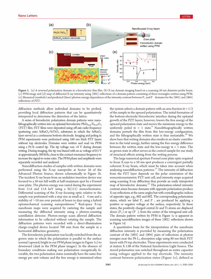
Nanodiffraction studies of samples with written domains wereperformed using the X-ray nanoprobe at Sector 26 of theAdvanced Photon Source, shown schematically in Figure 1b.The incident X-ray beam from an undulator insertion device wasfocused to a 50 nm full width at half-maximum spot by a Fresnelzone plate. The photon energy was varied during the experimentfrom 11.6 and 11.8 keV using a Si(111) monochromator.Differential scanning of the X-ray focusing optic relative to thesample was performed with a step size as small as 2�4 nm and astability of ∼10 nm over periods of hours to days using a hybridoptomechanical scanning nanopositioner.8 Real-space X-raynanobeam maps were acquired by rastering the sample andmeasuring the diffracted intensity using a photon-countingscintillation detector. Photon-energy scans allowed diffractioninformation to be collected without rotating the sample. Thediffraction patterns were recorded with a direct-illuminationcharge-coupled device located 700 mm from the sample in ahorizontal diffraction geometry.
The ferroelectric polarization was locally switched from the as-grown state in which the polarization is parallel to the surfacenormal (upward, bright in our PFMphase images in Figure 1c) todownward (dark in the PFM phase images). In the absence ofboundary conditions making one polarization energetically fa-vorable, the two polarization states nominally have the same freeenergy per unit volume and the free energy is minimized when
the system selects a domain pattern with an area fractionR = 1/2of the sample in the upward polarization. The initial formation ofthe bottom-electrode/ferroelectric interface during the epitaxialgrowth of the PZT layers, however, lowers the free energy of theupward polarization state and moves the minimum energy to theuniformly poled R = 1 state.9 Nanolithographically writtendomains perturb the film from this low-energy configuration,and the lithographically written state is thus metastable.10 Weshow here that writing domains also results in an elastic contribu-tion to the total energy, further raising the free energy differencebetween the written state and the low-energy R = 1 state. Theas-grown state in effect serves as the control sample for our studyof structural effects arising from the writing process.
The large numerical aperture Fresnel zone plate optic requiredto focus X-rays to a 50 nm spot produces a convergent partiallycoherent X-ray beam, which must be taken into account whenanalyzing nanodiffraction patterns.11 The intensity of diffractionfrom the PZT layer depends on the polar orientation of thenoncentrosymmetric PZT unit cell, and intensity maps acquiredusing scanning X-ray diffraction thus provide an easily interpretedmap of ferroelectric domains.12 The polarization-related intensitycontrast arises because domains with opposite polarization produceX-ray reflections at the same angles but with crystallographic indicesof opposite sign, e.g., 002 and 002. The corresponding polarizationstates, which we label P+ and P�, are produced by applying apositive or negative voltage at the surface, respectively. In thesestates, the positively charged central Zr and Ti atoms are displaceddown (P+) or up (P�), from the center of the tetragonal unit cell.The domain pattern written by PFM in Figure 1c is apparent inscanning nanodiffraction images of these {002} reflections shownin Figure 1d.
A quantitative basis for the interpretation of the nanobeamdiffraction intensity is provided by measuring the polarizationcontrast of the {003} and {004} pairs of reflections at photonenergies near the Pb L3 absorption edge using 80 nm thick PZTlayers with Pt top electrodes. These experiments were conductedat station X-13B of the National Synchrotron Light Source. Thestored polarization was switched throughout an entire capacitorusing voltages applied to the top electrode. The intensitycontrast between polarization states (Figure 1e), defined as
Figure 1. (a) A reversed polarization domain in a ferroelectric thin film. (b) X-ray domain imaging based on a scanning 50 nm diameter probe beam.(c) PFM image and (d) map of diffracted X-ray intensity using {002} reflections of a domain pattern consisting of three rectangles written using PFM.(e)Measured (symbols) and predicted (lines) photon-energy dependence of the intensity contrast between P+ and P� domains for the {003} and {004}reflections of PZT.
3082 dx.doi.org/10.1021/nl2009873 |Nano Lett. 2011, 11, 3080–3084
Nano Letters LETTER
(I(P+)� I(P�))/(I(P+)), agrees with a kinematic X-ray diffractionprediction using bulk atomic positions, a random-alloy distributionof Zr and Ti, and tabulated atomic scattering factors.13�15 The signof the contrast between polarization states, in particular, is differentbetween families of reflections {00l} in which l is odd (as {003})
and reflections with even l (e.g., {004}). The sign of the intensitycontrast between domains in Figure 1d shows directly and crystal-lographically that nanolithography with a positive tip voltage haswritten domains with the expected polarity.
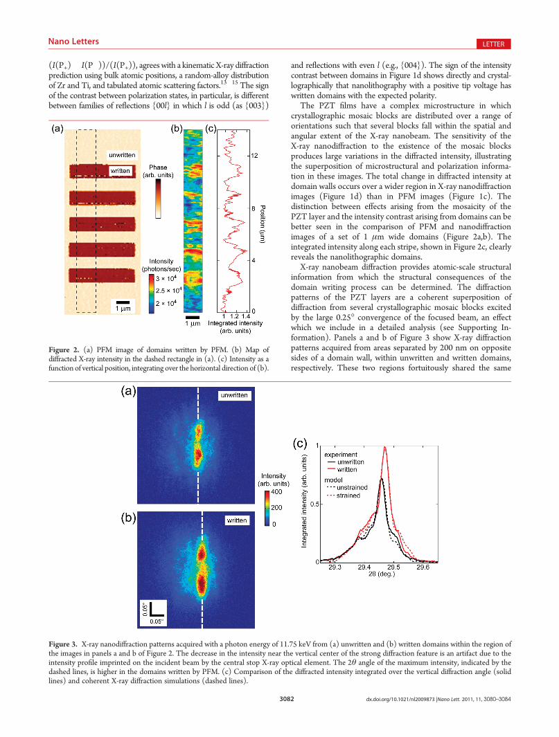
The PZT films have a complex microstructure in whichcrystallographic mosaic blocks are distributed over a range oforientations such that several blocks fall within the spatial andangular extent of the X-ray nanobeam. The sensitivity of theX-ray nanodiffraction to the existence of the mosaic blocksproduces large variations in the diffracted intensity, illustratingthe superposition of microstructural and polarization informa-tion in these images. The total change in diffracted intensity atdomain walls occurs over a wider region in X-ray nanodiffractionimages (Figure 1d) than in PFM images (Figure 1c). Thedistinction between effects arising from the mosaicity of thePZT layer and the intensity contrast arising from domains can bebetter seen in the comparison of PFM and nanodiffractionimages of a set of 1 μm wide domains (Figure 2a,b). Theintegrated intensity along each stripe, shown in Figure 2c, clearlyreveals the nanolithographic domains.
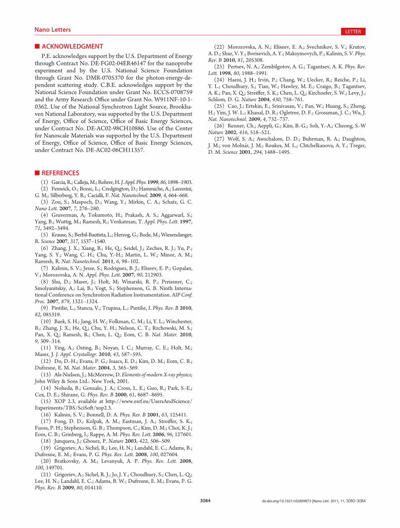
X-ray nanobeam diffraction provides atomic-scale structuralinformation from which the structural consequences of thedomain writing process can be determined. The diffractionpatterns of the PZT layers are a coherent superposition ofdiffraction from several crystallographic mosaic blocks excitedby the large 0.25� convergence of the focused beam, an effectwhich we include in a detailed analysis (see Supporting In-formation). Panels a and b of Figure 3 show X-ray diffractionpatterns acquired from areas separated by 200 nm on oppositesides of a domain wall, within unwritten and written domains,respectively. These two regions fortuitously shared the same
Figure 2. (a) PFM image of domains written by PFM. (b) Map ofdiffracted X-ray intensity in the dashed rectangle in (a). (c) Intensity as afunction of vertical position, integrating over the horizontal direction of (b).
Figure 3. X-ray nanodiffraction patterns acquired with a photon energy of 11.75 keV from (a) unwritten and (b) written domains within the region ofthe images in panels a and b of Figure 2. The decrease in the intensity near the vertical center of the strong diffraction feature is an artifact due to theintensity profile imprinted on the incident beam by the central stop X-ray optical element. The 2θ angle of the maximum intensity, indicated by thedashed lines, is higher in the domains written by PFM. (c) Comparison of the diffracted intensity integrated over the vertical diffraction angle (solidlines) and coherent X-ray diffraction simulations (dashed lines).

3083 dx.doi.org/10.1021/nl2009873 |Nano Lett. 2011, 11, 3080–3084
Nano Letters LETTER
mosaic block structure. The diffraction patterns from the writtenand unwritten areas differ at large values of 2θ, the angle betweenthe directions of the average incident beam and the observeddiffracted beam. The difference can be seen in the diffractionpatterns in panels a and b of Figure 3 as well as in the integrated2θ dependence of the intensity in Figure 3c. The coherentdiffraction analysis shows that the difference in intensity at high2θ angles arises from a compressive strain in written areas.
The 2θ angles associated with the central peaks of nanodif-fraction patterns do not provide a reliable estimate of the strainbecause the 2θ angle at which these reflections are observeddepends on the random local orientations of individual mosaicblocks. The possibility that the shift to higher 2θ angles is due to asystematic change in the orientation of the mosaic blocks as aresult of the domain writing process can be eliminated, however,by examining the photon energy dependence of the diffractionpatterns, as described in the Supporting Information. A simula-tion gives excellent agreement with the observed diffractionpatterns (dashed line, Figure 3c), with the assumption that thediffraction patterns consist of sharp reflections from coherentdiffractions of two large mosaic blocks and a broad reflectionfrom a large number of smaller blocks.
The difference in lattice spacing between written and unwrit-ten domains can be more easily measured using the shift in thehigh-2θ edge of the diffraction patterns. Doing this allows us toextend the analysis of the diffraction pattern to a more generalcase in which we are not restricted to analyze regions with iden-tical mosaic block structures. The compressive strain reaches0.1% in the center of written domains with respect to the unwrittenareas. The spatial variation of the strain is shown in Figure 4a,matching the phase of the PFM response acquired in the samelocations (Figure 4b).
The compressive strain in written domains can be explained bynoting that the surface charge of the written domains may not becompletely compensated and that a depolarization field in theopposite direction of polarization can be developed within thewritten domains.16 Air, dielectrics, and even conductors cannotcompletely compensate the polarization charge.17,18 The writtendomains are compressively strained due to the electromechanicalresponse to this charge. The electric field accompanying thestrain induced by writing can be determined via the piezoelectriccoupling. With a piezoelectric coefficient of 45 pm/V,19 theobserved 0.1% strain corresponds to a depolarization field of220 kV/cm. This electric field is smaller than the low-frequencycoercive field and is thus not sufficient by itself to completelydestabilize the P+ domain.
The compressive strain developed during ferroelectric nano-lithography raises the free energy of the written domains and canlead to the destabilization of small ferroelectric nanodomains.The combination of this strain and the built-in field raise the freeenergy of the written domains, making the written state meta-stable. Only the relative difficulty of nucleating and growingdomains of the lower-energy P� polarization prevents a loweringof the free energy by the production of a single domain state. Thelarge 1 μm domains written for these experiments thus persistover long intervals of weeks or more and appear in PFM imagesacquired after the X-ray studies. Smaller domains, however, canbe expected to be considerably less stable. The dynamics of thedecay of macroscopic polarization in the analogous two-dimen-sional thin film geometry has been studied extensively.20,21 Theformation and decay of domains written nanolithographically byPFM involve an inherently more complicated distribution of
fields but follow similar considerations.22 The decay of thewritten polarization state will be sped by the additional elasticenergy we have found here.
X-ray nanodiffraction measurements show that local nano-scale structural effects can have a profound impact in scanningprobe nanolithography and on future prospects for understand-ing and control of nanoscale phenomena. The evaluation of thedistortions resulting from nanolithography leads to the futureopportunity to develop nanotechnologies that allow the use ofnanoscale variations in strain to select the ground state of fer-roelectrics, dielectrics, and other complex oxides.23�25 In addi-tion, extensions of this approach will allow a detailed explorationof the connections between growth conditions, the selectionof the direction of the ferroelectric polarization via these condi-tions, and the role of defects in the stability of domains. Thematch in length scales between the spatial resolution of X-raynanoprobes and scanning probe lithography promises to revealstructural effects in emerging nanomaterial systems in whichsubtle degrees of freedom can be patterned at small scales includingorbital and charge order26 as well as ferromagnetic, ferrimagnetic,and antiferromagnetic moments.27
’ASSOCIATED CONTENT
bS Supporting Information. Coherent diffraction simula-tion and distinguishing between strain and crystallographicrotation using the photon-energy-dependence of the diffractionpattern. This material is available free of charge via the Internet athttp://pubs.acs.org.
’AUTHOR INFORMATION
Corresponding Author*E-mail: [email protected].
Present Addresses^School ofMaterials Science and Engineering, Gwangju Instituteof Science and Technology, Gwangju 500-712, Korea.
Figure 4. (a) Piezoelectric phase observed using PFM. (b) Compres-sive strain along a vertical line within the dashed rectangle in Figure 2a.
3084 dx.doi.org/10.1021/nl2009873 |Nano Lett. 2011, 11, 3080–3084
Nano Letters LETTER
’ACKNOWLEDGMENT
P.E. acknowledges support by the U.S. Department of Energythrough Contract No. DE-FG02-04ER46147 for the nanoprobeexperiment and by the U.S. National Science Foundationthrough Grant No. DMR-0705370 for the photon-energy-de-pendent scattering study. C.B.E. acknowledges support by theNational Science Foundation under Grant No. ECCS-0708759and the Army Research Office under Grant No. W911NF-10-1-0362. Use of the National Synchrotron Light Source, Brookha-ven National Laboratory, was supported by the U.S. Departmentof Energy, Office of Science, Office of Basic Energy Sciences,under Contract No. DE-AC02-98CH10886. Use of the Centerfor Nanoscale Materials was supported by the U.S. Departmentof Energy, Office of Science, Office of Basic Energy Sciences,under Contract No. DE-AC02-06CH11357.
’REFERENCES
(1) Garcia, R.; Calleja,M.; Rohrer,H. J. Appl. Phys.1999, 86, 1898–1903.(2) Fenwick, O.; Bozec, L.; Credgington, D.; Hammiche, A.; Lazzerini,
G. M.; Silberberg, Y. R.; Cacialli, F. Nat. Nanotechnol. 2009, 4, 664–668.(3) Zou, S.; Maspoch, D.; Wang, Y.; Mirkin, C. A.; Schatz, G. C.
Nano Lett. 2007, 7, 276–280.(4) Gruverman, A; Tokumoto, H.; Prakash, A. S.; Aggarwarl, S.;
Yang, B.; Wuttig, M.; Ramesh, R.; Venkatesan, T. Appl. Phys. Lett. 1997,71, 3492–3494.(5) Krause, S.; Berbil-Bautista, L.; Herzog, G.; Bode,M.;Wiesendanger,
R. Science 2007, 317, 1537–1540.(6) Zhang, J. X.; Xiang, B.; He, Q.; Seidel, J.; Zeches, R. J.; Yu, P.;
Yang, S. Y.; Wang, C. H.; Chu, Y.-H.; Martin, L. W.; Minor, A. M.;Ramesh, R. Nat. Nanotechnol. 2011, 6, 98–102.(7) Kalinin, S. V.; Jesse, S.; Rodriguez, B. J.; Eliseev, E. P.; Gopalan,
V.; Morozovska, A. N. Appl. Phys. Lett. 2007, 90, 212903.(8) Shu, D.; Maser, J.; Holt, M; Winarski, R. P.; Preissner, C.;
Smolyanitskiy, A.; Lai, B.; Vogt, S.; Stephenson, G. B. Ninth Interna-tional Conference on Synchrotron Radiation Instrumentation.AIP Conf.Proc. 2007, 879, 1321–1324.(9) Pintilie, L.; Stancu, V.; Trupina, L.; Pintilie, I. Phys. Rev. B 2010,
82, 085319.(10) Baek, S. H.; Jang, H. W.; Folkman, C. M.; Li, Y. L.; Winchester,
B.; Zhang, J. X.; He, Q.; Chu, Y. H.; Nelson, C. T.; Rzchowski, M. S.;Pan, X. Q.; Ramesh, R.; Chen, L. Q.; Eom, C. B. Nat. Mater. 2010,9, 309–314.(11) Ying, A.; Osting, B.; Noyan, I. C.; Murray, C. E.; Holt, M.;
Maser, J. J. Appl. Crystallogr. 2010, 43, 587–595.(12) Do, D.-H.; Evans, P. G.; Isaacs, E. D.; Kim, D. M.; Eom, C. B.;
Dufresne, E. M. Nat. Mater. 2004, 3, 365–369.(13) Als-Nielsen, J.; McMorrow, D. Elements of modern X-ray physics;
John Wiley & Sons Ltd.: New York, 2001.(14) Noheda, B.; Gonzalo, J. A.; Cross, L. E.; Guo, R.; Park, S.-E.;
Cox, D. E.; Shirane, G. Phys. Rev. B 2000, 61, 8687–8695.(15) XOP 2.3, available at http://www.esrf.eu/UsersAndScience/
Experiments/TBS/SciSoft/xop2.3.(16) Kalinin, S. V.; Bonnell, D. A. Phys. Rev. B 2001, 63, 125411.(17) Fong, D. D.; Kolpak, A. M.; Eastman, J. A.; Streiffer, S. K.;
Fuoss, P. H.; Stephenson, G. B.; Thompson, C.; Kim, D. M.; Choi, K. J.;Eom, C. B.; Grinberg, I.; Rappe, A. M. Phys. Rev. Lett. 2006, 96, 127601.(18) Junquera, J.; Ghosez, P. Nature 2003, 422, 506–509.(19) Grigoriev, A.; Sichel, R.; Lee, H. N.; Landahl, E. C.; Adams, B.;
Dufresne, E. M.; Evans, P. G. Phys. Rev. Lett. 2008, 100, 027604.(20) Bratkovsky, A. M.; Levanyuk, A. P. Phys. Rev. Lett. 2008,
100, 149701.(21) Grigoriev, A.; Sichel, R. J.; Jo, J. Y.; Choudhury, S.; Chen, L.-Q.;
Lee, H. N.; Landahl, E. C.; Adams, B. W.; Dufresne, E. M.; Evans, P. G.Phys. Rev. B 2009, 80, 014110.
(22) Morozovska, A. N.; Eliseev, E. A.; Svechnikov, S. V.; Krutov,A. D.; Shur, V. Y.; Borisevich, A. Y.;Maksymovych, P.; Kalinin, S. V. Phys.Rev. B 2010, 81, 205308.
(23) Pertsev, N. A.; Zembilgotov, A. G.; Tagantsev, A. K. Phys. Rev.Lett. 1998, 80, 1988–1991.
(24) Haeni, J. H.; Irvin, P.; Chang, W.; Uecker, R.; Reiche, P.; Li,Y. L.; Choudhury, S.; Tian, W.; Hawley, M. E.; Craigo, B.; Tagantsev,A. K.; Pan, X. Q.; Streiffer, S. K.; Chen, L. Q.; Kirchoefer, S. W.; Levy, J.;Schlom, D. G. Nature 2004, 430, 758–761.
(25) Cao, J.; Ertekin, E.; Srinivasan, V.; Fan, W.; Huang, S.; Zheng,H.; Yim, J. W. L.; Khanal, D. R.; Ogletree, D. F.; Grossman, J. C.; Wu, J.Nat. Nanotechnol. 2009, 4, 732–737.
(26) Renner, Ch.; Aeppli, G.; Kim, B.-G.; Soh, Y.-A.; Cheong, S.-WNature 2002, 416, 518–521.
(27) Wolf, S. A.; Awschalom, D. D.; Buhrman, R. A.; Daughton,J. M.; von Moln�ar, J. M.; Roukes, M. L.; Chtchelkanova, A. Y.; Treger,D. M. Science 2001, 294, 1488–1495.