structural and magnetic properties of epitaxial la sr0 ...structural and magnetic properties of...
TRANSCRIPT

Structural and magnetic properties of epitaxial La0.67Sr0.33MnO3 films and nanostructures
Mercy Mathews

PROMOTIECOMMISSIE: VOORZITTER: prof. dr. ir. J. Huskens University of Twente, TNW SECRETARIS: prof. dr. ir. A. Bliek University of Twente, TNW PROMOTOR(EN): prof. dr. ing. D.H.A. Blank University of Twente, TNW prof. dr. J. C. Lodder University of Twente, EWI ASSISTANT PROMOTOR(EN):
dr. R. Jansen dr. ing. A.J.H.M. Rijnders
University of Twente, EWI University of Twente, TNW
REFERENT:
dr. K. Steenbeck Institut für Photonische Technologien, Germany
LEDEN: prof. dr. J. Aarts Leiden University prof. dr. P. Kelly University of Twente, TNW dr. L. Abelmann University of Twente, EWI
Insti tute for Nanotechnology The research described in this thesis was carried out in the Inorganic Materials Science group and Nanoelectronics group of the MESA+ Institute for Nanotechnology, University of Twente, P.O. Box 217, 7500 AE, Enschede, The Netherlands. This research was funded by the Netherlands Nanotechnology network, NANOIMPULS and NANONED, supported by the ministry of economic affairs, The Netherlands. Printed by Wöhrmann Print Service, Loskade 4, 7202 CZ, Zutphen The Netherlands. © Mercy Mathews, Enschede, 2007 No part of this work may be reproduced by print, photocopy or any other means without the permission in writing from the publisher. ISBN: 978-90-365-2590-9 Cover page illustration: Front side; Three-dimensional AFM images of LSMO nanowires of different dimensions on STO substrates. Top one is having width 422nm, height 26nm and periodicity 600nm, left one is having width 292nm height 25nm and periodicity 600nm, and right one is having width 146nm, height 43nm and periodicity 600nm. Back side; Three-dimensional AFM image of LSMO nano dots of diameter 300nm, height 44nm and periodicity 600nm.

STRUCTURAL AND MAGNETIC PROPERTIES OF EPITAXIAL
La0.67Sr0.33MnO3 FILMS AND NANOSTRUCTURES
DISSERTATION
to obtain the doctor’s degree at the University of Twente,
on the authority of the rector magnificus, prof. dr. W.H.M. Zijm,
on account of the decision of the graduation committee, to be publicly defended
on Thursday 22 November 2007 at 13.15hrs
by
Mercy Mathews
born on 13th march 1979 in Thrickodithanam, India

This dissertation is approved by: Promoters: Prof. dr. ing. D.H.A. Blank and Prof. dr. J.C. Lodder Assistant-promoters: Dr. R. Jansen, and Dr. ing. A.J.H.M. Rijnders

To my Parents, Shajichayan and Maria


7
Contents 1. Introduction……………………………….………………………
11
1.1 Outline of the thesis ………………………………………………… 13 1.2 References ……………………………………………………………
14
2. Survey of La0.67Sr0.33MnO3 half-metallic ferromagnets…………..
17
2.1 La0.67Sr0.33MnO3 ……………………………………………………… 17 2.2 Structural properties of LSMO thin film on different substrates……... 20 2.3 Magnetic properties of epitaxial LSMO thin films …………………... 22
2.4 References……………………………………………………………..
25
3. Experimental Techniques………..………………………………..
29
3.1 Introduction…………………………………………………………… 29 3.2 Deposition of Epitaxial oxide films …………………………………... 30 3.2.1 Pulsed Laser Deposition (PLD) ………….…………………... 30 3.2.2 PLD set up…………….……………………………………… 31 3.2.3 Substrate materials and special surface treatments…………... 32 3.3 Structural characterization methods…………………………………... 34 3.3.1 In situ reflection high-energy electron diffraction (RHEED)... 34 3.3.2 X-ray Diffraction (XRD)…………….……………………….. 35 3.3.3 Atomic Force Microscopy (AFM)…………………………… 37 3.4 Magnetic characterization…………………………………………...... 37 3.4.1 Vibrating sample magnetometry (VSM)…………………….. 37 3.4.2 Torque magnetometry ……………………...………………... 38 3.4.3 Magnetic force microscopy(MFM)……….………………….. 40 3.5 Laser Interference Lithography (LIL)………………………………... 41
References………………………………………………………………….
43
4. La0.67Sr0.33MnO3 films on vicinal SrTiO3 (001) substrates……….
45
4.1 Introduction…………………………………………………………… 45

8
4.2 Deposition conditions…………………………………………………. 46 4.3 Growth and structural properties……………………………………… 47 4.3.1 Growth characterization ……………………………………... 47 4.3.2 Surface morphology of LSMO film………………………….. 48 4.3.3 Structural analysis …………………………………………… 50 4.4 Magnetic properties…………………………………………………… 53 4.4.1 Hysteresis loops……………………………………………..... 53 4.4.2 Magnetization vs Temperature……………………………….. 55 4.4.3 Magnetic anisotropy ……………….………………………… 56 4.4.4 Analysis by torque Measurements…………………………… 60 4.5 Magnetic force microscopy (MFM) ………………………………….. 64 4.5 Conclusions……………………………………………………………. 65 4.6 References………………………………………………………….......
66
5. La0.67Sr0.33MnO3 films on NdGaO3 substrates……………………….
69
5.1 Introduction…………………………………………………………… 69 5.2 Growth and structural properties……………………………………… 70 5.2.1 Crystal structure of NdGaO3(NGO).......................................... 70 5.2.2 Growth and surface analysis…………………………………. 77 5.2.3 Structural analysis……………………………………………. 80 5.3 Magnetic properties…………………………………………………… 83 5.3.1 Magnetization vs Temperature……………………………….. 83 5.3.2 Magnetic anisotropy ……………….………………………… 84 5.3.3 Magnetization reversal mechanism…………………………... 89 5.3.4 Magnetic force microscopy (MFM) …………………………. 93 5.4 Conclusions…………………………………………………………… 95
5.5 References……………………………………………………………..
96
6. Preparation and characterization of La0.67Sr0.33MnO3 nanowires/dots.
99
6.1 Introduction……………………………..…………………………….. 99 6.2 Optimization of Laser Interference Lithography and ion beam etching 100 6.3 Patterned La0.67Sr0.33MnO3 (LSMO) nanostructures on SrTiO3 (STO).. 103 6.3.1 Magnetic anisotropy……………………….............................. 104 6.3.2 Magnetization vs temperature………………………………... 114 6.3.3 Magnetic force microscopy of nanowires and dots ………….. 115 6.4 Patterned La0.67Sr0.33MnO3 (LSMO) nanowires on NdGaO3 .............. 118 6.4.1 LSMO nanowires on NGO(110)……………………………... 118 6.4.2 LSMO nanowires on NGO(010)…………………………….. 119 6.4.1.1 Magnetic anisotropy……………………………………. 120 6.4.3 Magnetic force microscopy…………………………………... 121 6.5 Conclusions…………………………………………………................ 123
6.6 References…………………………………………………………….
125
7. Conclusions …………………………………………...................
127
7.1 Introduction……………………………………………….…………... 127

9
7.2 La0.67Sr0.33MO3 films on SrTiO3 substrates……………........................ 128 7.3 La0.67Sr0.33MO3 films on NdGaO3 substrates...........................……....... 128
7.4 La0.67Sr0.33MO3 nanowires and dots........................................................ 130 7.5 References……………………………………………………………..
131
Summary……………………………………………………………………………………
133
Samenvatting (Summary in dutch)………………………………………..
137
Acknowledgments…………………………………………………………...
141
Curriculum Vitae…………………………………………………………. 143

10

Chapter 1
Introduction
In this introductory chapter, a brief summary of the main aim and the scope of the thesis are given. In addition, the selection criteria for the model system of LSMO to prepare thin films and the importance of its nanostructuring are briefly discussed. Finally the outline of the thesis is given.
Recent years have witnessed a tremendous growth of research in the field of spintronics, in view of its obvious potential for novel devices with entirely new capabilities[1-5]. In this context, phenomena such as giant magnetoresistance (GMR), colossal magnetoresistance (CMR), spin-tunneling in junctions (STJ), and more recently, spin coherence and spin dephasing have attracted significant attention[6-10]. Since the discovery of CMR effect in perovskite mixed valence manganites La1-xMxMnO3 (R = rare earth, M = Ca, Sr, Ba, Pb), the magnetic, electronic and transport properties of these materials and their relations to microstructures have attracted much interest[11, 12]. Historically, in the fifties, the mixed-valence perovskites La1−xMxMnO3 were studied, both experimentally [13] and theoretically [14, 15]. Different attractive properties of CMR manganites have been extensively described and discussed in review papers[7, 16]. Because of the large magnetoresistance effect and strong spin polarization at the fermi level, these oxides can be used in magnetoresistive devices, such as magnetic random access memory and sensors[17, 18]. However for a great number of these possible industrial applications, these materials have to be prepared in thin film form and because of this reason many research work is being carried out to get the best structural and physical properties of these thin films. Composition of thin films, oxygen content, film thickness, lattice strains induced by the lattice mismatch, and so on, have crucial role in determining its magnetic and transport properties[19-21]. In this thesis, we have investigated thin films and two dimensional arrays of nanostructures of La(1-x)SrxMnO3(LSMO), which can be considered as the model system of CMR manganites.

Introduction
12
LSMO is characteristic of the class of Mn perovskites which display an extremely high degree of spin polarization, making them possible candidates for magnetic-based devices which exploit spin polarized electron transport. The transport properties of these ferromagnets appear to be related to strong interactions among charge, spin and lattice degrees of freedom. The electronic properties of LSMO, as described by band theory, are nearly half-metallic[22, 23]. The concept of half metallic ferromagnetism means that the conduction electrons that are 100% spin polarized. That is, only one of the two spin bands is partially occupied at the Fermi level while the other has zero density of states across the Fermi level. The half-metallic properties of LSMO are of great importance for applications in spintronics. Due to the high spin polarization of carriers, the spin dependent tunneling between two ferromagnetic manganite electrodes across a thin insulating barrier should produce a large magneto-resistance response. Tunnel junction of LSMO/SrTiO3/LSMO shows magnetoresistance in excess of 1800% at a temperature of 4K corresponding to a tunnel spin polarization of 95%. Nevertheless, the magneto resistance seem to vanish at room temperature[24]. In particular, the electronic structure of LSMO is determined by the competition of double exchange and superexchange interactions, charge/orbital ordering instabilities and strong coupling with the lattice deformations. Moreover, they have high conductivity and good thermal stability with maximum curie temperature (Tc) of 370K at Sr doping concentration, x = 0.33[25]. They may be employed as electrodes for ferroelectric and dielectric capacitors in future dynamic random access memory applications[26, 27]. Although there are many applications of thin films of LSMO, very few studies are carried out in the fabrication and analysis of structural and magnetic properties of nanostructures of LSMO.
Magnetic nanostructures are used in patterned magnetic media, magnetic devices and materials for microwave applications and also it provides a model system for the study of magnetic interactions and switching behavior. Ferromagnetic nanostructures exhibit unique and tunable magnetic properties that are very different from those of bulk ferromagnetic materials, and thin films. New advances in lithography and magnetic domain imaging techniques have facilitated these studies and enabled their application to a wide range of magnetic materials.
Magnetism of the CMR manganites at the nanoscale, when the size of the structures is comparable to or smaller than the ferromagnetic (FM) domain size (~150nm), offers an important area for research. Moreover in modern technology, there are techniques capable of producing nanometer-sized structures over large areas. Understanding the nature of magnetism at the nanometer length scale in these materials is of interest from a fundamental perspective and for the development of next generation spin-based devices. The realization of spin-based devices requires high density, ordered arrays of magnetic materials with a high degree of spin polarization at surfaces.

Introduction
13
Geometrical confinement of epitaxial LSMO films into nanodots and nanowires may change the strain state and thus affect the magnetic and transport properties. The finite size effects such as enhancement of coercivity and decrease in curie temperature of the nanostructures are a few of the possible changes when the magnetic material is patterned into nanostructures. For example, change in shape of the hysteresis loops is seen in patterned structures compared to thin film of LSMO[28]. Stripe domains are seen in LSMO islands on LAO substrates[28, 29]. They form due to the competition between magneto-static and magneto crystalline anisotropy energies. In these films perpendicular anisotropy energy is large enough to overcome the magneto-static energy to give stripe domains. The patterning of thin film to nanodots does indeed facilitate the rotation of moments in to the out of plane direction[28]. Recently, Takamura et al have fabricated highly spin polarized complex magnetic oxide nanostructures embedded in a paramagnetic matrix by electron beam lithography and ion implantation[30]. In this study, it is shown that the domain patterns can be controlled by changing the shape and size of the LSMO islands, film thickness and the relative magnitudes of the magneto-crystalline and magneto-elastic energies through the choice of the STO substrate orientation. The main aim of this thesis is to study the exceptional structural and magnetic properties of epitaxial LSMO thin films grown in controlled layer by layer growth mode by pulsed lased deposition on different single crystalline substrates namely SrTiO3 and NdGaO3. Deposition conditions and structural quality of the film has a notable influence on its magnetic properties. These epitaxial LSMO films can show many interesting magnetic properties such as magnetization and magnetic anisotropy depending on many factors such as temperature, vicinal steps, and the change in strain state when different substrates are used. Next main goal is to pattern these high quality thin films into nanowires and nanodots in order to study the resulting changes of the magnetic properties compared to thin films which in turn can be interesting for its applicability to future spintronic devices. 1.1 Outline of the thesis In the research illustrated in the following chapters, magnetic and structural studies of LSMO thin films and nanostructures on different substrates are described. Pulsed laser deposition (PLD) technique is employed to fabricate LSMO thin films and laser interference lithography (LIL) technique is used for patterning it into nanostructures. In chapter 2, a brief overview of the recent research works in LSMO thin films is given which can provide a starting point to the research work which is explained in later chapters. LSMO thin films on various substrates prepared by different deposition techniques show many interesting

Introduction
14
magnetic properties determined by number of factors such as film composition, oxygen gas pressure, film thickness, substrate induced lattice strain etc which needs to be explored more.
The experimental techniques used in this thesis are summarized in chapter 3. The growth technique, pulsed laser deposition, and reflection high energy electron diffraction, a surface sensitive technique to analyze the film surface during growth are briefly described. Also different ex-situ characterization techniques are presented, which are used to define the structural, and magnetic properties of the as-deposited thin films. In addition, the patterning technique (laser interference lithography) is also briefly explained in this chapter. In chapter 4, investigations on LSMO thin films grown on SrTiO3 (STO) substrates are presented. STO substrates having TiO2 surface termination was used for LSMO deposition. These thin films grown by PLD are analyzed for its structural and magnetic properties. Magnetic measurements were carried out especially to analyze the magnetic anisotropy properties of the films of varied thicknesses at different temperature. Substrates having vicinal surface, with varied step directions were used to study the influence of surface steps (ie; the broken symmetry on the surface) on magnetic anisotropy of the films.
Magnetic and structural studies on LSMO films grown on NdGaO3 (NGO) substrates of different orientations are presented in chapter 5. The structural studies were done by X-ray diffraction (XRD), Reflection high energy diffraction (RHEED) and Atomic force microscopy (AFM) measurements on films on different NGO substrates. Magnetic anisotropy of all the films on NGO(100), (010), (110) and (001) substrates was extensively studied. The influence of vicinal steps and different strain states on the magnetic anisotropy of LSMO films on NGO substrates of all the three orientations was also analyzed. Magnetization reversal mechanism of these films was studied using two different theoretical models.
In chapter 6, fabrication and magnetic studies of LSMO nanowires and nanodots on STO and NGO substrates are discussed. Nanodots and wires fabricated on STO substrates were having diameter and width down to 80nm and 125nm respectively. Nanowires fabricated on NGO substrates are with width down to 146nm. Magnetic measurements of nanowires on STO substrates were done by both vibrating sample magneto meter (VSM) and torque magneto meter (TM) to study the magnetic anisotropy and magnetization versus temperature. Different magnetic properties of nanowires/dots and thin films on both STO and NGO substrates are compared and analyzed. Finally in chapter 7, main conclusions of this thesis are given.
Introduction
15
1.2 References 1. A. Ruotolo, F. Miletto Granozio, A. Oropallo, G.P. Pepe, P. Perna, U. Scotti di
Uccio, D. Pullini and G. Innocenti and P. Perlo, Novel low-field magnetoresistive devices based on manganites. Journal of magnetism and magnetic materials, 2006. 310: p. e684-e686.
2. W. Eerenstein, M. Wiora, J. L. Prieto, J. F. Scott and N. D. Mathur, Giant sharp and persistent converse magnetoelectric effects in multiferroic epitaxial heterostructures. Nature Materials, 2007. 6 p. 348-351.
3. H. Yamada, Y. Ogawa, Y. Ishii, H. Sato, M. Kawasaki, H. Akoh and and Y. Tokura, Engineered Interface of Magnetic Oxides Science 2004. 305: p. 646-648.
4. M. Gajek, M. Bibes, S. Fusil, K. Bouzehouane, J. Fontcuberta, A. Barthélémy and A. Fert, Tunnel junctions with multiferroic barriers. Nature Materials 2007. 6: p. 296 - 302.
5. J. M. De Teresa, A. Barthélémy, A. Fert, J. P. Contour, F. Montaigne and and P. Seneor, Role of Metal-Oxide Interface in Determining the Spin Polarization of Magnetic Tunnel Junctions. Science, 1999. 286: p. 507-509.
6. Y. Ishii, H. Yamada, H. Sato, H. Akoh, Y. Ogawa, M. Kawasaki and Y. Tokura, Improved tunneling magnetoresistance in interface engineered (La,Sr)MnO[sub 3] junctions. Applied Physics Letters, 2006. 89(4): p. 042509.
7. A. P. Ramirez, Colossal magnetoresistance. Journal of Physics: Condensed Matter, 1997. 9: p. 8171-8199.
8. M. Bowen, A. Barthelemy, M. Bibes, E. Jacquet, J. P. Contour, A. Fert, F. Ciccacci, L. Duo and R. Bertacco, Spin-Polarized Tunneling Spectroscopy in Tunnel Junctions with Half-Metallic Electrodes. Physical Review Letters, 2005. 95(13): p. 137203.
9. B. Beschoten, E. Johnston-Halperin, D. K. Young, M. Poggio, J. E. Grimaldi, S. Keller, S. P. DenBaars, U. K. Mishra, E. L. Hu and D. D. Awschalom, Spin coherence and dephasing in GaN. Physical Review B, 2001. 63(12): p. 121202.
10. R. Bratschitsch, Z. Chen, S. T. Cundiff, E. A. Zhukov, D. R. Yakovlev, M. Bayer, G. Karczewski, T. Wojtowicz and J. Kossut, Electron spin coherence in n-doped CdTe/CdMgTe quantum wells. Applied Physics Letters, 2006. 89(22): p. 221113.
11. R. von Helmolt, J. Wecker, B. Holzapfel, L. Schultz and K. Samwer, Giant negative magnetoresistance in perovskitelike La2/3Ba1/3MnOx ferromagnetic films. Physical Review Letters, 1993. 71(14): p. 2331.
12. J. Fontcuberta, B. Martínez, A. Seffar, S. Piñol, J. L. García-Muñoz and X. Obradors, Colossal Magnetoresistance of Ferromagnetic Manganites: Structural Tuning and Mechanisms. Physical Review Letters, 1996. 76(7): p. 1122.
13. E. O. Wollan and W. C. Koehler, Neutron Diffraction Study of the Magnetic Properties of the Series of Perovskite-Type Compounds [(1-x)La,xCa]MnO3. Physical Review, 1955. 100(2): p. 545.
14. P. G. de Gennes, Effects of Double Exchange in Magnetic Crystals. Physical Review, 1960. 118(1): p. 141.
15. John B. Goodenough, Theory of the Role of Covalence in the Perovskite-Type Manganites [La,nbspM(II)]MnO3. Physical Review, 1955. 100(2): p. 564.
16. M. Viret and S. von Molnar J. M. D. Coey and Adv. Phys., 1999. 48: p. 167. 17. Ll. Balcells, E. Calvo and and J. Fontcuberta, Room-temperature anisotropic
magnetoresistive sensor based on manganese perovskite thick films. Journal of Magnetism and Magnetic Materials, 2002. 242-245: p. 1166-1168.

Introduction
16
18. J.-B. Park, G.-S. Park, I.-Y. Song, J.-S. Bae, J.-E. Lee, J.-H. Yoo, Y. Murakami and D. Shindo, Analysis of magnetic microstructure in MRAM bits by electron holography and Lorentz microscopy. Journal of Electron Microscopy, 2006. 55(1): p. 17-21.
19. J. Z. Sun, D. W. Abraham, R. A. Rao and C. B. Eom, Thickness-dependent magnetotransport in ultrathin manganite films. Applied Physics Letters, 1999. 74(20): p. 3017-3019.
20. J. Li, C. K. Ong, J. M. Liu, Q. Huang and S. J. Wang, Oxygen-deficiency-activated charge ordering in La2/3Sr1/3MnO3-δ thin films. Applied Physics Letters, 2000. 76(8): p. 1051-1053.
21. M. Rajeswari, R. Shreekala, A. Goyal, S. E. Lofland, S. M. Bhagat, K. Ghosh, R. P. Sharma, R. L. Greene, R. Ramesh, T. Venkatesan, and T. Boettcher, Correlation between magnetic homogeneity, oxygen content, and electrical and magnetic properties of perovskite manganite thin films. Applied Physics Letters, 1998. 73(18): p. 2672-2674.
22. G. Banach and W.M. Temmerman, Half-Metallicity of LSMO. Condensed Matter, 2003. 0308272.
23. G. Banach and W. M. Temmerman, Delocalization and charge disproportionation in La(1 - x)SrxMnO3. Physical Review B (Condensed Matter and Materials Physics), 2004. 69(5): p. 054427.
24. M. Bowen, M. Bibes, A. Barthelemy, J. P. Contour, A. Anane, Y. Lemaitre and A. Fert, Nearly total spin polarization in La2/3Sr1/3MnO3 from tunneling experiments. Applied Physics Letters, 2003. 82(2): p. 233-235.
25. A. Urushibara, Y. Moritomo, T. Arima, A. Asamitsu, G. Kido and Y. Tokura, Insulator-metal transition and giant magnetoresistance in La1-xSrxMnO3. Physical Review B, 1995. 51(20): p. 14103.
26. X. G. Tang, Q. X. Liu, Y. P. Jiang, R. K. Zheng and H. L. W. Chan, Enhanced dielectric properties of highly (100)-oriented Ba(Zr,Ti)O3 thin films grown on La0.7Sr0.3MnO3 bottom layer. Journal of Applied Physics, 2006. 100(11): p. 114105.
27. C. Feng, H. F. Wang, Q. Z. Liu, W. Wenbin and X. G. Li, Fabrication of epitaxial and transparent Pb(Zr[sub 0.52]Ti0.48)O3 ferroelectric capacitors with La0.07Sr0.93SnO3 electrodes. Applied Physics Letters, 2007. 90(8): p. 082904.
28. Yan Wu, Y. Matsushita and Y. Suzuki, Nanoscale magnetic-domain structure in colossal magnetoresistance islands. Physical Review B, 2001. 64(22): p. 220404.
29. W. Olson Trevor, M. W. Olson Jeanine, Scholl Andreas and Y. Suzuki, Magnetic domain structure of colossal magnetoresistance thin films and islands. Journal of applied physics, 2004. 95: p. 7354-7356.
30. Y. Takamura, R. V. Chopdekar, A. Scholl, A. Doran, J. A. Liddle, B. Harteneck and and Y. Suzuki, Tuning Magnetic Domain Structure in Nanoscale La0.7Sr0.3MnO3 Islands. Nano letters, 2006. 6(6): p. 1287-1291.

Chapter 2
Survey of La0.67Sr0.33MnO3 half-metallic ferromagnets
A brief description about the different fundamental properties of the manganite La0.67Sr0.33MnO3 (LSMO) is presented in this chapter. Also, pre-existing studies on magnetic behaviors such as the magnetic anisotropy and domain structures of LSMO thin films grown on different substrates are briefly explained. 2.1 La0.67Sr0.33MnO3
Doped perovskite manganites have renewed interest because they exhibit a variety of unique magnetic, electronic and transport behaviors such as colossal magneto resistance (CMR), spin/charge/orbital ordering and high degree of spin polarization and so on[1-3]. Half-metallic ferromagnetic materials appear as potential candidates for spintronic devices, and much work is under progress to synthesize magnetic oxides, such as La0.67Sr0.33MnO3 (LSMO)[4-7]. The electronic phase diagram (shown in figure 2.1(a)) of LSMO reveals that it has an anti-ferromagnetic and insulating behavior at high and low doping concentration (x) values and ferromagnetic metallic behavior in a certain range of concentrations centered around x ≈ 0.33 with highest curie temperature (Tc = 370K) [8]. So it is considered for the use in various devices such as magnetic field sensors and hard disk read heads. Since the density of states at the Fermi level (EF) in LSMO is occupied mostly by the majority-spin electrons alone in the ferromagnetic (FM) and metallic states, attempts have been made to use this almost 100% spin polarization in the form of heterostructures such as tunnel junctions[9-11]. Moreover, due to the hole doping in LSMO, many interesting device applications have been proposed based on LSMO[12]. Traditionally, LSMO has been grown on substrates such as
Survey of La0.67Sr0.33MnO3 half metallic ferromagnets
18
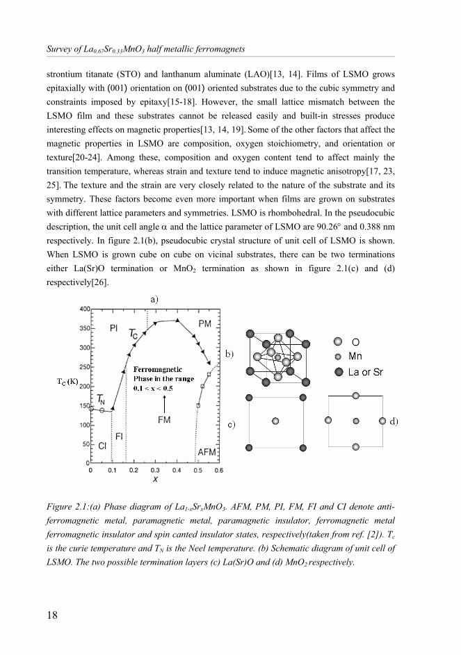
strontium titanate (STO) and lanthanum aluminate (LAO)[13, 14]. Films of LSMO grows epitaxially with (001) orientation on (001) oriented substrates due to the cubic symmetry and constraints imposed by epitaxy[15-18]. However, the small lattice mismatch between the LSMO film and these substrates cannot be released easily and built-in stresses produce interesting effects on magnetic properties[13, 14, 19]. Some of the other factors that affect the magnetic properties in LSMO are composition, oxygen stoichiometry, and orientation or texture[20-24]. Among these, composition and oxygen content tend to affect mainly the transition temperature, whereas strain and texture tend to induce magnetic anisotropy[17, 23, 25]. The texture and the strain are very closely related to the nature of the substrate and its symmetry. These factors become even more important when films are grown on substrates with different lattice parameters and symmetries. LSMO is rhombohedral. In the pseudocubic description, the unit cell angle α and the lattice parameter of LSMO are 90.26° and 0.388 nm respectively. In figure 2.1(b), pseudocubic crystal structure of unit cell of LSMO is shown. When LSMO is grown cube on cube on vicinal substrates, there can be two terminations either La(Sr)O termination or MnO2 termination as shown in figure 2.1(c) and (d) respectively[26].
Figure 2.1:(a) Phase diagram of La1-xSrxMnO3. AFM, PM, PI, FM, FI and CI denote anti-ferromagnetic metal, paramagnetic metal, paramagnetic insulator, ferromagnetic metal ferromagnetic insulator and spin canted insulator states, respectively(taken from ref. [2]). Tc is the curie temperature and TN is the Neel temperature. (b) Schematic diagram of unit cell of LSMO. The two possible termination layers (c) La(Sr)O and (d) MnO2 respectively.

Survey of La0.67Sr0.33MnO3 half metallic ferromagnets
19
The early theoretical studies on manganites were considering the qualitative aspects of experimentally discovered results namely the increase in conductivity upon the polarization of the spins. Treatments of physics of this system have focused primarily on the double exchange (DE) mechanism proposed by Zener[27]. The double-exchange mechanism is a theory that predicts the relative ease with which an electron may be exchanged between two species. The DE process was explained historically in two ways. In the first way, there are two simultaneous motion of electrons involving up spin electron moving from oxygen to the Mn4+ ion and up spin electron moving from Mn3+ ion to the oxygen as shown by arrows in the figure 2.2(b) and can be schematically written as +
↑↓↑++
↓↑+↑ ⇒ 3
23,144
3,231 MnOMnMnOMn .
The second way to visualize DE was involving a second order process in which the two states described above go from one to the other using an intermediate state +
↑↓+↑
323
31 MnOMn [28]. In
LSMO, the 180 degree interaction of Mn-O-Mn in which the Mn "eg" orbitals are directly interacting with the O "2p" orbitals as shown in figure 2.2(a) and (b). The ferromagnetism and the close magnetic correlation of transport property in LSMO were traditionally understood within the framework of the Mn3+–O–Mn4+ double-exchange mechanism, in which a mobile eg electron can align the local core spins (S=3/2, t3
2g) ferromagnetically via a strong on-site Hund’s coupling and the eg electrons in turn become more itinerant due to the local spin alignment (Figure 2.2(a)). When the eg electrons directly jump from Mn to Mn their kinetic energy is minimized if all spins are aligned giving rise to ferromagnetism and metallicity to the material[2].
Figure 2.2:(a) Field splitting of the five-fold degenerate atomic 3d levels into lower t2g and higher eg levels for Mn3+ and Mn4+ where the orbital interactions namely Hund’s coupling (JH), hopping or transfer integral(t) and anti-ferromagnetic direct exchange(AF) is denoted. (b) Sketch of the double Exchange mechanism which involves two Mn ions and one O ion. The mobility of eg electrons improves if the localized spins are polarized. Taken from ref. [2].
eg
t2g
JH JH
t
JAF
Mn3+ Mn4+
a) b)
eg
t2g
JH JH
t
JAF
Mn3+ Mn4+
eg
t2g
JH JH
t
JAF
eg
t2g
JH JH
t
eg
t2g
JH JH
eg
t2g
eg
t2g
JH JH
t
JAF
Mn3+ Mn4+
a) b)

Survey of La0.67Sr0.33MnO3 half metallic ferromagnets
20
The physical properties of perovskite- type manganites especially LSMO are determined by two main parameters: the doping level of Strontium, x(Sr)= Mn4+/(Mn3++Mn4+), which determines the Mn3+/Mn4+ ratio and the average size of the cation A, <rA>. For a perfect size match between the La atoms and dopant atoms, the tolerance factor (t) = dA-O/√2 dMn-O = 1 and the Mn-O-Mn bond angle will be 180º. The curie temperature (TC) is maximum around x = ⅓ and for <rA> ≈ 1.24Å which is for La0.7Sr0.3MnO3 and here the Mn-O-Mn bond angle is 166.3º[2, 29]. The reduction of <rA> from this optimum value leads to an increase in distortion of the crystallographic structure which weakens the ferromagnetic double exchange and increases the tendency to localize the charge carriers[29]. The magnetic and transport properties of manganite thin films are very sensitive to its micro structure, growth conditions, and the lattice strain induced by the underlying substrate[21, 30-32]. Subsequently in this chapter, pre-existing studies and more recent developments of LSMO are discussed which are relevant for our work on the same. 2.2 Structural properties of LSMO thin film on different substrates
LSMO films have been grown by pulsed laser deposition on various substrates, such as single crystal LaAlO3 (LAO)(001), NdGaO3 (NGO)(110) and SrTiO3 (STO)(001)[21, 33]. Figure 2.3 gives the θ–2θ XRD patterns of the LSMO films on these substrates[33]. In the films on all these substrates, only the (00l) peaks are present. This reveals that the LSMO film is highly c-axis oriented and strained on these substrates and the c-axis lattice constants of the LSMO on LAO, NGO, and STO calculated from the x-ray data are 3.930, 3.906, and 3.855 Å, respectively[33]. The LSMO lattice experiences a biaxial tensile strain on STO substrate. The strain on LAO is biaxial compressive and on NGO is uniaxial compressive[21, 33].
The films deposited on various other substrates, such as MgO(001), SiO2/Si(001) and amorphous quartz, by using a magnetron DC sputtering system has been also studied earlier[19]. According to the X-ray diffraction patterns, LSMO films grown on MgO, SiO2/Si and amorphous quartz are seen to be polycrystalline and less textured because of the large lattice mismatch. The semi conductor-metal transition temperature for ‘c’ axis oriented LSMO/STO and LSMO/LAO films is found to be around the curie temperature (≈365K). But these transition temperatures of the polycrystalline LSMO films grown on different substrates like MgO, SiO2/Si and quartz are lowered down even to 200 K[19]. It is notable that the curie temperatures (TC) of these films are about 365 K. Hence, TMI deviates from the TC of the polycrystalline LSMO films. The c-axis oriented LSMO films exhibit typical transport properties, in which the resistance gradually increases with temperature and reaches its

Survey of La0.67Sr0.33MnO3 half metallic ferromagnets
21
maximum at the curie temperature. But the polycrystalline LSMO films show significantly different behaviors of the temperature-dependent resistance, and the magnetoresistance[19].
Figure 2.3: θ-2θ XRD patterns of the LSMO films on single crystals of (a) LaAlO3 (001), (b) NGO(001), (c) SrTiO3 (001). Taken from ref. [33] .
The magnetic and transport studies of LSMO thin films on SrTiO3 substrate, which
were prepared at different oxygen pressure and of different thicknesses reveals that these properties are more sensitive to oxygen pressure than on film thicknesses. Reduced value of oxygen partial pressure is associated with the oxygen defect that leads to magnetic and structural inhomogeniety[21]. It was found that an increased oxygen pressure during deposition increased the homogeneity of the film and a decrease of the c-axis lattice constant when LSMO film is grown on LAO substrate[21]. This indicates that there might be a connection between oxygen content and lattice strain in the films. Lattice strain can also be affected by oxygen vacancies. One reason is that the Mn-O-Mn bond angles and Mn-Mn bond distance will change depending on the oxygen content in the film. Increased oxygen deficiency in LSMO leads to a negative electric charge deficiency which is compensated by a Mn4+ decrease to keep the charge neutrality. So increased oxygen deficiency also decreases the Mn4+/Mn3+ ratio[34]. Oxygen vacancies will make the bending of local Mn-O-Mn bond chain and as a result the conduction bandwidth decreases significantly. Thus sample resistivity increases and metal to insulator transition temperature decreases to lower temperature. Lattice distortions and even phase transitions (e.g. from quasi-cubic to tetragonal and to orthorhombic structure) can be observed in LSMO films due to these oxygen deficiencies[20]. It is seen that with decreasing film thickness the curie temperature (TC)

Survey of La0.67Sr0.33MnO3 half metallic ferromagnets
22
decreases and the peak resistivity increases[21, 31, 35, 36]. Both these effects indicate that the Mn-O-Mn double exchange interaction is weakened.
The epitaxial LSMO films (aLSMO bulk ~ 3.885Å where “a” is lattice parameter) on LaAlO3 (LAO) (aLAO ~ 3.789Å) and SrTiO3 (STO) (aSTO ~ 3.905Å) are, respectively under in-plane biaxial compressive strain and in-plane biaxial tensile strain[13, 14, 19, 33]. On the other hand, LSMO films grown on NdGaO3 (NGO) (orthorhombic, a/√2 = 3.873, b/√2 = 3.890, c/2 = 3.853 Å) has in-plane uniaxial compressive strain as only one of the in-plane lattice parameter is different from that of LSMO lattice constant[21]. Although one film is under tensile strain (LSMO/STO, Lattice mismatch,δ = (asubstrate – aLSMO)/asubstrate = +0.8%) and one is under compressive strain (LSMO/LAO, Lattice strain = -2.6%)[21], the trends for resistivity and metal to insulator transition temperature(TMI) of these LSMO films with thickness are the same[13]. It has been found that saturation magnetization of LSMO on LAO is larger than LSMO on STO. These differences in the saturation magnetization can be understood by the internal ‘pressure’ consequent upon lattice mismatch. That is compressive stress increases saturation magnetization and decreases ‘peak’ resistivity while the tensile stress in sample on STO acts in the opposite way[13]. Thin films on LAO are under compressive strain that will increase the deviation of the Mn-O-Mn angle from its ideal value[29, 37], lowering the TMI. The tensile stress on films on STO will decrease the deviation of the bond angle, which would increase the TMI, but in order to decrease the strain in the film, oxygen vacancies are introduced which will decrease the strain, but also lower the metal to insulator transition temperature because there will be fewer Mn4+ ions[38]. 2.3 Magnetic properties of epitaxial LSMO thin films
Single crystals of LSMO have cubic perovskite structure with a rhombohedral
distortion and a rhombohedral lattice constant 7.78Å. The magnetic anisotropy of (001) and (110) LSMO films on (001) and (110) STO substrates were also already studied[16, 17]. (001) LSMO films of thickness in the range 500-3000Å clearly show the easy and hard axis along [100] and [110] directions respectively which is illustrated in figure 2.4. (Here it should be noted that the easy direction of LSMO unit cell is described by some authors[16] as [110] direction and by some other authors as [100] direction[39]. It is because their definitions of axes are different. Some people consider Mn-O bond direction as [100] axis and the other consider one side of the unit cell as [100] axis. And here in this thesis, we use the latter definition.
The fourfold symmetry or biaxial anisotropy shown by this film can be explained by either cubic magneto crystalline or stress anisotropy not by rhombohedral magneto isotropy[16, 17]. In (001) LSMO films, the magneto elastic energy or biaxial elastic modulus

Survey of La0.67Sr0.33MnO3 half metallic ferromagnets
23
is isotropic in the plane of the film and therefore the magnetic anisotropy is dominated by crystal structure effects. So, for (001) LSMO films, easy in plane direction will be [110] and equivalent directions. And in plane [100] and [010] directions are hard[39].
Figure 2.4: Remanence vs field angle φ of a (001) LSMO film on (001) STO at room temperature. The field is applied in the plane of the film as a function of angle φ as shown in the inset. The sample was initially poled positive and then the magnetization measurements were made at 1 kOe and zero field. Taken from ref. [16]. It is reported that 250Å LSMO film grown on STO substrate exhibits in-plane magnetic anisotropy below a TC of ~320K because the out of plane magnetization is considerably smaller than the magnetization values taken along two in-plane crystal directions ([100] and [110]) as seen in figure 2.5(a)[40]. At temperatures below ~250K (indicated by the arrow in figure 2.5(a)), the measured magnetization along the [100] edge direction deviates from the behavior along the [110], indicating that an in-plane biaxial anisotropy develops with in-plane <110> axes magnetically easy [40].
The film of thickness 250Å grown on NGO(110) substrate develops ferromagnetism below ~340K with an in-plane unaxial anisotropy along one of the edges of the substrate, as indicated in figure 2.5(b)[40]. Below ~30K, a weak biaxial anisotropy develops in the system. In other words, samples grown on NGO substrates exhibit both uniaxial and biaxial anisotropies in the growth plane with their relative strengths that are temperature dependent[40].
A remarkable feature of the LSMO film is that the slight difference in strain induced by the underlying substrate leads to a drastic change in magnetic domain images which can be taken by magnetic force microscopy (MFM)[13, 14, 33]. In Figure 2.6, local magnetic microstructures of LSMO thin films on NGO and STO substrates imaged by MFM

Survey of La0.67Sr0.33MnO3 half metallic ferromagnets
24
measurements are shown[33]. The MFM image on LSMO/STO shows feather-like magnetic patterns with negligible magnetic contrast, which is typical of a film with an in-plane magnetization. Magnetic stripe domains is found with almost straight line shape in LSMO film on NGO(110) confirming that the film has uniaxial in-plane magnetic anisotropy. On the other hand, some other studies on LSMO films grown on NGO(110) shows 'feather' like magnetic contrast in magnetic force microscopy (MFM) images which is characteristic of films with in-plane magnetic anisotropy[14].
Figure 2.5: Field-cooled temperature-dependent magnetization at 5Oe of 250Å La0.67Sr0.33MnO3 epitaxial films grown on (a) SrTiO3(001) and (b) NdGaO3(110). The responses were measured along three symmetry directions. The directions with respect to the substrate are: (a) in-plane [110] (open circles), in-plane [100] (closed circles), and out-of-plane [001] (triangles). (b) in-plane edge directions (closed and opened circles), and out-of-plane (triangles). Arrows indicate the spin reorientation transitions. Taken from ref. [40].
Figure 2.6: MFM images of La0.7Sr0.3MnO3 thin films, taken in zero applied field at room temperature, on two different substrates of (a) NGO, and (b) STO. The scan size is 4X4 µm. Taken from ref. [33].
a) b)a) b)
(a) (b)
STO NGO
(a) (b)(a) (b)
STO NGO
Survey of La0.67Sr0.33MnO3 half metallic ferromagnets
25
It is reported that for LSMO films grown on STO substrates, although the coercivity is rather low (HC< 10mT), the magnetic saturation value is reached only for fields larger than 200mT[41]. These high saturation fields suggest that some parts of the film (presumably at interfaces level) have different coercivity compared to the ‘bulk’ of the film. The low coercivity of the film suggests that there are very small nucleation fields[41]. By polarized neutron reflectometry it is observed that the magnetization is clearly inhomogeneous through the thickness of the film and decreases markedly when approaching the bottom and top interfaces of the film[41]. Looking into literature and finding the promising properties of LSMO, which is not fully described in this chapter, many efforts have been directed towards making magnetic tunnel junctions out of this material. Magnetic tunnel junctions, consisting of two half-metallic ferromagnets (say LSMO) separated by an insulating thin layer are studied by many researchers in order to realize its application in magnetic random access memory (MRAM) and read heads. Besides a very large tunnel magnetoresistance (TMR) at low temperatures reported by Bowen et al[4] who found spin polarization of LSMO as 95%, the TMR ratio for LSMO/STO/LSMO junctions reported so far was not large enough, in general, to be associated with the half-metallicity of LSMO. Also, TMR was rapidly suppressed with increasing temperature and typically disappeared around 215 K[42-44]. One of the possible origins of such decreased TMR is the formation of the dead layer near the LSMO/STO interface, in which the ferromagnetism of LSMO is locally deteriorated. This is explained by the model that the charge transfer at the valence-mismatched interface induces a hole-overdoped LSMO layer which is dominated by the antiferromagnetic spin canting[45]. By preventing or compensating the charge transfer by interface engineering approaches the TMR response is greatly improved[11, 46]. So it will be beneficial to study the magnetic and structural properties of LSMO films grown on different substrates which may provide different electronic structure at the interface. 2.4 References 1. A. P. Ramirez, Colossal magnetoresistance. Journal of Physics: Condensed Matter,
1997. 9: p. 8171-8199. 2. E. Dagotto, T. Hotta and A. Moreo, Colossal magnetoresistance materials: the key
role of phase separation. Physics Reports, 2001. 344: p. 1-153. 3. J. Fontcuberta, B. Martínez, A. Seffar, S. Piñol, J. L. García-Muñoz and X.
Obradors, Colossal Magnetoresistance of Ferromagnetic Manganites: Structural Tuning and Mechanisms. Physical Review Letters, 1996. 76(7): p. 1122.
4. M. Bowen, M. Bibes, A. Barthelemy, J. P. Contour, A. Anane, Y. Lemaitre and A. Fert, Nearly total spin polarization in La2/3Sr1/3MnO3 from tunneling experiments. Applied Physics Letters, 2003. 82(2): p. 233-235.

Survey of La0.67Sr0.33MnO3 half metallic ferromagnets
26
5. E. Gommert, H. Cerva, A. Rucki, R. v. Helmolt, J. Wecker, C. Kuhrt and K. Samwer, Structure and magnetoresistive properties in La--manganite thin films. Journal of Applied Physics, 1997. 81: p. 5496-5498.
6. J. Li, C. K. Ong, J. M. Liu, Q. Huang and S. J. Wang, Oxygen-deficiency-activated charge ordering in La2/3Sr1/3MnO3-δ thin films. Applied Physics Letters, 2000. 76(8): p. 1051-1053.
7. M. Gajek, M. Bibes, S. Fusil, K. Bouzehouane, J. Fontcuberta, A. Barthélémy and and A. Fert, Tunnel junctions with multiferroic barriers. Nature Materials, 2007. 6: p. 296 - 302.
8. A. Urushibara, Y. Moritomo, T. Arima, A. Asamitsu, G. Kido and Y. Tokura, Insulator-metal transition and giant magnetoresistance in La1-xSrxMnO3. Physical Review B, 1995. 51(20): p. 14103.
9. J. M. De Teresa, A. Barthélémy, A. Fert, J. P. Contour, R. Lyonnet, F. Montaigne, P. Seneor and A. Vaurès, Inverse Tunnel Magnetoresistance in Co/SrTiO3/La0.7Sr0.3MnO3: New Ideas on Spin-Polarized Tunneling. Physical Review Letters, 1999. 82(21): p. 4288.
10. L. Samet, D. Imhoff, J.-L. Maurice, J.-P. Contour, A. Gloter, T. Manoubi, A. Fert and and C. Colliex, EELS study of interfaces in magnetoresistive LSMO/STO/LSMO tunnel junctions. The European Physical Journal B, 2003. 34: p. 179-192.
11. H. Yamada, Y. Ogawa, Y. Ishii, H. Sato, M. Kawasaki, H. Akoh and and Y. Tokura, Engineered Interface of Magnetic Oxides Science, 2004. 305: p. 646-648.
12. A. Tiwari, C. Jin, D. Kumar and J. Narayan, Rectifying electrical characteristics of La0.7Sr0.3MnO3/ZnO heterostructure. Applied Physics Letters, 2003. 83(9): p. 1773-1775.
13. C. Kwon, M.C. Robson, K.-C. Kim, J.Y. Gu, S.E. Lofland, S.M. Bhagat, Z. Trajanovic, M. Rajeswari, T. Venkatesan, A.R. Kratz, R.D. Gomez, and R. Ramesh, Stress-induced effects in epitaxial (La0.7Sr0.3)MnO3 films. Journal of Magnetism and Magnetic Materials, 1997. 172: p. 229-236.
14. R. Desfeux, S. Bailleul, A. Da Costa, W. Prellier and A. M. Haghiri-Gosnet, Substrate effect on the magnetic microstructure of La 0.7Sr0.3MnO3 thin films studied by magnetic force microscopy. Applied Physics Letters, 2001. 78(23): p. 3681-3683.
15. J. Z. Sun, D. W. Abraham, R. A. Rao and C. B. Eom, Thickness-dependent magnetotransport in ultrathin manganite films. Applied Physics Letters, 1999. 74(20): p. 3017-3019.
16. Y. Suzuki, H. Y. Hwang, S. W. Cheong and R. B. van Dover, The role of strain in magnetic anisotropy of manganite thin films. Applied Physics Letters, 1997. 71(1): p. 140-142.
17. Y. Suzuki, H. Y. Hwang, S. W. Cheong, T. Siegrist, R. B. van Dover, A. Asamitsu and Y. Tokura, Magnetic anisotropy of doped manganite thin films and crystals. Journal of Applied Physics, 1998. 83: p. 7064-7066.
18. Y. Wu, Y. Suzuki, U. Rudiger, J. Yu, A. D. Kent, T. K. Nath and C. B. Eom, Magnetotransport and magnetic domain structure in compressively strained colossal magnetoresistance films. Applied Physics Letters, 1999. 75(15): p. 2295-2297.
19. S. Y. Yang, W. L. Kuang, Y. Liou, W. S. Tse, S. F. Lee and Y. D. Yao, Growth and characterization of La0.7Sr0.3MnO3 films on various substrates. Journal of Magnetism and Magnetic Materials, 2004. 268(3): p. 326-331.
20. J-M Liu, Y X Zhang, Z G Liu, Y W Du, H H Zhang, Z Yu and C K Ong, Oxygen-deficiency-activated anomalous transport in La2/3Sr1/3MnO3-δ thin films deposited by laser ablation. Journal of Physics:Condensed Matter, 2002. 14: p. 3167.

Survey of La0.67Sr0.33MnO3 half metallic ferromagnets
27
21. D. Joonghoe, N. H. Hur, I. S. Kim and Y. K. Park, Oxygen pressure and thickness dependent lattice strain in La0.7Sr0.3MnO3 films. Journal of Applied Physics, 2003. 94(12): p. 7670-7674.
22. M. Kawasaki, M. Izumi, Y. Konishi, T. Manako and and Y. Tokura, Perfect epitaxy of perovskite manganite for oxide spin-electronics. Materials science and Engineering B, 1999. 63(1-2): p. 49-57.
23. L. Malavasi, M.C. Mozzati, C.B. Azzoni C. Tealdi and and G. Flor, Cation doping and oxygen content dependence of magnetic properties in single layered La0.5Sr1.5MnO4 manganite. Journal of Magnetism and Magnetic Materials, 2006. 310(2): p. e193-e194.
24. L. Meda, L. Kennon, C. Bacaltchuk, H. Garmestani and K. H. Dahmen, Effects of thermal annealing on the texture of La0.67Sr0.33MnO3 thin films. Journal of Material Research, 2001. 16(7): p. 1887-1889.
25. Y.S. Du, B. Wang, T. Li, D.B. Yu and and H. Yana, Effects of annealing procedures on the structural and magnetic properties of epitaxial La0.7Sr0.3MnO3 films. Journal of Magnetism and Magnetic Materials, 2004. 297(2): p. 88-92.
26. A-M Haghiri-Gosnet and J-P Renard, CMR manganites: physics, thin films and devices. J. Phys. D: Appl. Phys., 2003. 36: p. R127-R150.
27. C. Zener, Interaction between the d-Shells in the Transition Metals. II. Ferromagnetic Compounds of Manganese with Perovskite Structure. Physical Review, 1951. 82(3): p. 403.
28. P. W. Anderson and H. Hasegawa, Considerations on Double Exchange. Physical Review, 1955. 100(2): p. 675.
29. H. Y. Hwang, S. W. Cheong, P. G. Radaelli, M. Marezio and B. Batlogg, Lattice Effects on the Magnetoresistance in Doped LaMnO3. Physical Review Letters, 1995. 75(5): p. 914.
30. N.M. Souza-Neto, A.Y. Ramos, H.C.N. Tolentino, E. Favre-Nicolin and L. Ranno, Local effects in strained manganite thin films. Journal of Alloys and Compounds, 2004. 369: p. 205-208.
31. J. F. Bobo, D. Magnoux, R. Porres, B. Raquet, J. C. Ousset, A. R. Fert, Roucau Ch, P. Baules, M. J. Casanove and E. Snoeck, Structural, magnetic, transport, and magneto-optical properties of single crystal La2/3Sr1/3MnO3 thin films. Journal of Applied Physics, 2000. 87: p. 6773-6775.
32. H. L. Ju, M. Krishnan Kannan and D. Lederman. Evolution of strain-dependent transport properties in ultrathin La0.67Sr0.33MnO3 films. 1998: AIP.
33. D. Joonghoe, Y. N. Kim, Y. S. Hwang, J. C. Kim and N. H. Hur, Strain-induced magnetic stripe domains in La0.7Sr0.3MnO3 thin films. Applied Physics Letters, 2003. 82(9): p. 1434-1436.
34. R. Cauro, A. Gilabert, J. P. Contour, R. Lyonnet, M. G. Medici, J. C. Grenet, C. Leighton and Ivan K. Schuller, Persistent and transient photoconductivity in oxygen-deficient La2/3Sr1/3MnO3-δ thin films. Physical Review B, 2001. 63(17): p. 174423.
35. M. Izumi, Y. Konishi, T. Nishihara, S. Hayashi, M. Shinohara, M. Kawasaki and Y. Tokura, Atomically defined epitaxy and physical properties of strained La0.6Sr0.4MnO3 films. Applied Physics Letters, 1998. 73(17): p. 2497-2499.
36. A. M. Haghiri-Gosnet, J. Wolfman, B. Mercey, Simon Ch, P. Lecoeur, M. Korzenski, M. Hervieu, R. Desfeux and G. Baldinozzi, Microstructure and magnetic properties of strained La0.7Sr0.3MnO3 thin films. Journal of Applied Physics, 2000. 88(7): p. 4257-4264.

Survey of La0.67Sr0.33MnO3 half metallic ferromagnets
28
37. A. Asamitsu, Y. Moritomo, Y. Tomioka, T. Arima and Y. Tokura, A structural phase transition induced by an external magnetic field. Nature, 1995. 373: p. 407 - 409
38. Y.P. Liu, Y.S. Du, M. Zhang, H. Yan and and Y.Y. Wang, Effect of internal strain on magnetic properties of La0.7Sr0.3MnO3 films. Vacuum, 2007. 81(7): p. 826-829.
39. L. M. Berndt, Balbarin Vincent and Y. Suzuki, Magnetic anisotropy and strain states of (001) and (110) colossal magnetoresistance thin films. Applied Physics Letters, 2000. 77(18): p. 2903-2905.
40. F. Tsui, M. C. Smoak, T. K. Nath and C. B. Eom, Strain-dependent magnetic phase diagram of epitaxial La0.67Sr0.33MnO3 thin films. Applied Physics Letters, 2000. 76(17): p. 2421-2423.
41. F. Ott, M. Viret, R. Borges, R. Lyonnet, E. Jacquet, C. Fermon and J. -P. Contour, Interface magnetism of La0.7Sr0.3MnO3 thin films studied by neutron reflectometry. Journal of Magnetism and Magnetic Materials, 2000. 211(1-3): p. 200-205.
42. J. Hayakawa, K. Ito, S. Kokado, M. Ichimura, A. Sakuma, M. Sugiyama, H. Asano and M. Matsui. The origin of bias-voltage dependence in CoFe/SrTiO3/La0.7Sr0.3MnO3 magnetic tunnel junctions. 2002: AIP.
43. E. Favre-Nicolin, L. Ranno, C. Dubourdieu and and M. Rosina, Spin-dependent tunnelling in La0.7Sr0.3MnO3/SrTiO3 superlattices. Thin Solid Films, 2001. 400(1-2): p. 165-168.
44. M.-H. Jo, M. G. Blamire, D. Ozkaya and and A. K. Petford-Long, Spin- and charge-modulated trilayer magnetic junctions: La0.7Ca0.3MnO3/La0.45Ca0.55MnO3/La0.7Ca0.3MnO3. Journal of Physics: Condensed Matter, 2003. 15: p. 5243-5251.
45. M. Izumi, Y. Ogimoto, Y. Okimoto, T. Manako, P. Ahmet, K. Nakajima, T. Chikyow, M. Kawasaki and Y. Tokura, Insulator-metal transition induced by interlayer coupling in La0.6Sr0.4MnO3/SrTiO3 superlattices. Physical Review B, 2001. 64(6): p. 064429.
46. Y. Ishii, H. Yamada, H. Sato, H. Akoh, Y. Ogawa, M. Kawasaki and Y. Tokura, Improved tunneling magnetoresistance in interface engineered (La,Sr)MnO3 junctions. Applied Physics Letters, 2006. 89(4): p. 042509.

Chapter 3
Experimental Methods and Techniques
For the research work described in this thesis a number of experimental techniques and characterization methods are used. In this chapter, principles and descriptions of those experimental methods are given. First, we discuss the pulsed laser deposition technique and system used. Next, we present the microstructural and magnetization characterization methods. Finally, laser interference lithography technique which is used for patterning thin films to nanostructures is illustrated.
3.1 Introduction For most of the devices based on the epitaxial perovskite-type thin films and heterostructures, high-quality surfaces and distinct interfaces in between the constituent layers are usually prerequisite for good device performance. Therefore the deposition of high quality films and understanding the growth mechanism is very important. Epitaxial thin film fabrication of oxide materials are mostly done by one of the physical vapor deposition (PVD) technologies. Research in this thesis uses a special PVD technique called Pulsed Laser Deposition (PLD) method to grow thin films where high power laser beams ablates the material from a target. It is known that PLD has been used to deposit high quality films of wide variety of materials for more than a decade [1, 2]. PLD is used very efficiently for growth of metastable phases and artificial structures which are very difficult or impossible to be stabilized by means of conventional synthesis methods [3]. It has proved to be very effective for in situ fabrication of multi-component oxide heterostructures also [4]. Due to these reasons, PLD is widely used to grow La0.67Sr0.33MnO3 (LSMO) thin films on different crystalline substrates [5-7]. Moreover the growth of the monolayers can be followed by in situ Reflection high-electron energy diffraction (RHEED), which makes it possible to examine the precise stack of layers. The characterization of the thin films, after the fabrication process, can be performed with different analytical techniques which probe the

Experimental methods and techniques
30
structural, compositional, morphological and magnetic properties. Scanning probe microscopy (SPM), x-ray diffraction (XRD), vibrating sample magnetometry (VSM), magnetic Torque measurements, and magnetic force microscopy (MFM) are the characterization methods used in this thesis. With these experimental analysis techniques, it is not only possible to understand the growth, structure and magnetism in our thin films but also the relationship between them. We also fabricated patterned structures (dots and wires) from these high quality epitaxial films using Laser interference Lithography (LIL). In this chapter all fabrication and characterization techniques mentioned above will be presented and briefly discussed. 3.2 Deposition of epitaxial oxide films 3.2.1 Pulsed Laser deposition
Pulsed laser deposition (PLD) technique uses high power laser pulses to melt, evaporate and ionize material from the surface of a target, resulting in a dense vapor beam, which is a so called transient, highly luminous “plasma plume” that expands rapidly away from the target surface towards the substrate. The planar target is rotated or (x, y) - scanned in the focal plane of the laser beam to achieve a stationary ablation rate. The ablated material is collected on an appropriately placed substrate upon which it condenses and the thin film grows. The substrate is held stationary or is rotated for homogenization of the deposition rate; for particular film growth regimes the temperature of the substrate may be selected between room temperature and typically 1000ºC. A processing gas supply is often provided for the inlet of selected gases to produce desired chemical reactions during film growth.
The crystal quality and stochiometry of the final thin film depends mainly on the absorption/desorption, diffusivity and energy of the particles on the surface. In spite of this widespread usage, the fundamental processes occurring during the transfer of material from target to substrate are not fully understood and are consequently the focus of much research. Interest in the PLD technique escalated when it was found to be very well suited to the preparation of high critical temperature (High-Tc) oxide superconductors, but more widespread applications are emerging nowadays such as the deposition of permanent magnets, magneto-optic, magneto-electronic and piezoelectric materials [8-12].
Nd: YAG laser and Excimer lasers are usually used in PLD with a typical wavelength range of 200-400nm. As wavelengths decreases in this range, the absorption coefficient of the target material increases but the penetration depth decreases. This is a favorable situation because thinner layers of the target surface are ablated as the wavelength decreases towards 200nm.
Experimental methods and techniques
31
Some of the main advantages of PLD are;
1. As the laser source is outside the deposition chamber, it introduces minimal contamination to grown film.
2. With high power densities obtained by focusing the laser beams, high melting point materials can be vaporized at high deposition rates.
3. Simultaneous or sequential multi-source evaporation can be done easily by directing the laser beam with external mirrors.
4. Independent control of deposition parameters such as target to substrate distance, substrate temperature, deposition gas pressure, laser energy etc.
5. Stochiometry of target is maintained in thin films. 6. Deposition rate is highly controllable.
The main advantage of this method compared to other sputtering systems, is the stochiometric transfer of the material from target to substrate and excellent structural quality of the deposited film even at lower growth temperatures. Depending on the deposition parameters, the kinetic energy of the ablated particles can be controlled and there by the surface diffusivity and absorption/desorption probability of the adatoms arriving at the substrate or film surface can be controlled. This important aspect gives rise to a better crystallinity in comparison with conventional deposition techniques by using similar or lower substrate temperatures. As the laser used here is an external energy source, it is possible to use inert and reactive background gases like O2, O3, NO2 and N2O. The plasma plume of ablated material has a distribution, peaked towards the forward direction to the substrate. So thickness uniformity of the thin film is got only in a smaller angular range of ~1cm diameter. 3.2.2 PLD set-up
A schematic view of the deposition chamber is given in figure 3.1. The laser we used is the pulsed excimer, KrF laser (Lambda Physik LPX 210, Göttingen, Germany) with wavelength 248 nm, which operates at repetition frequencies of 1-100 Hz. The maximum pulse energy is 1000 mJ and width of the laser pulse is about 25ns. The pressure in the vacuum system during deposition is controlled by the effective pump speed and the total gas mass flow (0 – 40 ml/min). For the background gas, inert gas (Ar) as well as reactive gases (O2 and O3) was used. The amount of material ablated from the target surface is determined by the spot energy density and the spot size. To keep the spatial energy variation within this laser spot below 5%, a very small, homogenous part of the laser beam is selected by using a mask, which is projected onto the target under an incidence angle of 45° by means of a lens

Experimental methods and techniques
32
with a focal length of ~ 453 mm. By varying, both, the laser energy and the spot size on the target, the energy density at the target can be varied from 1.0 to 7.0 J/cm2.
Figure 3.1: Schematic diagram of pulsed laser deposition (PLD) set up. 3.2.3 Substrate materials and special surface treatments
ABO3 perovskite materials are excellent substrates for epitaxial growth of many other perovskite oxides. Both SrTiO3 and NdGaO3 are examples of the above mentioned ABO3 type oxides and their lattice parameters are ideal for epitaxial growth of LSMO films. To obtain epitaxial two dimensional growth mode of these films, fine control of the substrate surface morphology, the chemistry of terminating layer, as well as knowledge of its vicinal angle are important. The substrates which we have used here are (001) SrTiO3 as well as (110), (100), (010) and (001) NdGaO3. SrTiO3 is having a cubic perovskite structure and its prominent feature is the possibility to control its surface composition at the atomic level. SrTiO3 with TiO2 surface termination is an excellent choice as a starting substrate surface for the growth of atomically sharp interfaces. While NdGaO3 has an orthorhombic symmetry, (110) NdGaO3 can be represented as a perovskite-type pseudocubic crystal structure that is slightly distorted in comparison with the primitive perovskite structure. It has no structural phase transitions below 1500ºC[13]. Different reports are found about the substrate treatment of both STO and NGO[14, 15]. Both thermal and chemical treatments are employed to get atomically smooth substrate surfaces. The chemical treatment method is based on the difference in chemical reactivity of different surface components of the substrate. They are explained below for each substrate.
to pump
Vacuumdepositionchamber
TargetGas inlet
Plasma
Lens Mask
Substrate on heater
KrF excimer laser
Loadlock
Experimental methods and techniques
33
SrTiO3 (STO) For STO, chemical etching and thermal treatment method are used for its surface treatment. In this method, one of the surface oxides (i.e., the one with base character, here SrO) is selectively removed by means of a chemical reaction resulting in TiO2 termination at the surface[16]. The substrate is first cleaned in ethanol and it is soaked in demi water for 30 minutes. This results in the formation of Sr(OH)2 (SrO→Sr(OH)2 )on the surface of the substrate. The etching is done by the commercial buffered hydrogen fluoride solution (12.5 vol% HF + 87.5 vol% NH4F (BHF)) for 30 seconds and this result in TiO2 termination on the substrate surface. Then again the substrates are soaked in demi water for 20 minutes and cleaned with ethanol. All procedures done here are in ultrasonic bath. After these chemical procedures the substrate is annealed for 1 hour in 1bar of oxygen at 950ºC for the surface re-crystallization. NdGaO3 (NGO) For NGO, either thermal or chemical surface treatment was done depending on its orientation. Compared to the etching solution for SrTiO3, chemical solution of lower reactivity is used for NGO. A modified commercial buffered hydrogen fluoride solution is used for the chemical surface treatment of NGO substrate. Chemical treatment of (110) and (001) NdGaO3 substrates had to be done in solutions with different pH values, higher for former and lower for latter, respectively.
The pH value of the etching solution for NGO(001) should be in the range 5.0-5.5[15]. This solution is prepared by adding 20ml of commercial BHF + 3ml of NH4F + 110ml of demi water. The whole chemical treatment is the same as that of STO except the etching solution and the time period of etching. When the substrate is soaked in demi water for 30 minutes, Nd(OH)2 (NdO→Nd(OH)2 )forms on its surface and this gets removed during the etching process by the modified BHF resulting in GaO2-δ surface termination. Here the NGO(001) substrates are etched for 2 minutes and then annealed in 1000ºC for 1 hour in 1 bar of oxygen. The annealing procedure is performed for the surface re-crystallization.
For NGO(110), the etching solution consisted of 10ml commercial BHF + 4ml NH4F + 90ml demi water resulted in a pH of 4.0-4.5. Here also the chemical treatment is the same as that of STO except the etching solution which etches away the Nd(OH)2 formed on the substrate surface after soaking it in demi water. The time period of etching is 30 seconds for this substrate. After the chemical treatment these substrates were annealed in 950ºC for 1 hour in 1 bar of oxygen. NGO(100) and NGO(010)substrates are only thermally treated and no chemical treatment is done because there is no mixture of terraces with either GaO2-δ or NdO1+δ termination. (More details explained in chapter 5). These substrates are annealed for 1h at

Experimental methods and techniques
34
950ºC in 1 bar of oxygen. More details about the surface morphology of treated NGO substrates of different orientations are illustrated in chapter 5. 3.3 Structural characterization methods
In order to have a clear understanding of the thin film growth and to do the optimization of the deposition conditions, thorough analysis of the surface morphology and crystalline structure is necessary. Using RHEED, the morphology of the surface can be monitored during and after the growth of the film. By scanning probe microscopy (SPM), the quality of the surface can be analyzed in local areas, in more detail at the angstrom scale. The crystalline structure is characterized by x-ray diffraction (XRD).
3.3.1. In situ reflection high-energy electron diffraction (RHEED)
Reflection high-energy electron diffraction is a powerful technique for studying surface structures of flat surfaces[17, 18]. It enables direct exploration of the growth dynamics and surface morphology. RHEED is sensitive to surface changes, either due to structure changes or due to adsorption. Therefore, it is widely used as an in situ probe to monitor the growth of thin films both in research and in industry. Along with pulsed laser deposition we have used in situ high pressure RHEED where it is possible to use deposition pressure up to 0.5mbar. In the simple geometry of RHEED, an accelerated electron beam (5 – 100 keV) incidents on the surface with a glancing angle (< 3 deg) and is reflected. The high energy of the electrons would result in high penetration depth. However, because of the glancing angle of incidence, a few atomic layers are only probed. This is the reason of the high surface sensitivity of RHEED. Upon reflection, electrons diffract, forming a diffraction pattern on the phosphor screen that depends on the structure and the morphology of the probed surface. Features in this diffraction pattern explain the surface structure of the sample. If a surface is atomically flat, then sharp RHEED spots are seen. If the surface has a rougher surface, the RHEED pattern is more diffuse. During the growth of thin film on a substrate surface RHEED intensity shows an oscillation which determines the growth rate of the film. In the deposition setup the electron source and phosphor screen (as detector) are located far from the sample to avoid interference with the deposition process. 3.3.2 X-ray Diffraction
X-ray Diffraction data provides information regarding the crystalline structures of
different materials in bulk, powder and thin film forms. Such data can be used to determine
Experimental methods and techniques
35
the relative atomic positions of atoms of simple and complex materials. The crystalline structure can be analyzed by performing several scans, such as θ-2θ, (hkl) and φ−scans, to determine thickness, roughness and orientation. The XRD results reported in this thesis were carried out on the Philips X-ray diffractometer (X’pert, APD) or four-circle single crystal diffractometer (CAD4, Enraf Nonius, Delft, The Netherlands), both using the Cu-Kα radiation with the wavelength, λ = 1.54056 Å. The CAD4 system is a four circle diffractometer which is capable of measuring reciprocal space maps also. The following sections are descriptions of different types of XRD measurements used in this thesis.
High-angle measurements
It is the θ-2θ high-angle measurement which is explained here. A narrow and parallel X-ray beam comes from an X-ray source to a sample at an angle θ with respect to the film and a detector is placed at an angle 2θ with respect to the incident ray. During the measurement, the source is fixed while the sample and the detector are rotated so that the configuration θ-2θ is preserved. In the high-angle measurement, normally 2θ is scanned from about 20° to 120°, depending on the sample and the aim of the measurement. The recorded signal from the detector is plotted versus 2θ, which is called the high-angle XRD spectrum. During the measurement, a peak is observed at a certain angle 2θ when the Bragg condition is satisfied:
2d sin θ = nλ…………(3.1) where d is the lattice spacing of a set of crystallographic planes, parallel to the film plane; λ is the wavelength (1.5406Å). From all the peaks in the spectrum, we can get information about the orientation of the film with respect to the substrate and also the unit-cell out of plane lattice parameter ‘c’ of the thin film. The intensity of the peaks reveals the amount and quality of the texture. Low-angle measurements
Low-angle measurement is used to determine the thickness of the thin films. The low-angle measurement is in fact the same θ-2θ measurement but performed at low angles of 2θ, typically from 1° to 3°. In the obtained spectrum, we can see regular peaks which are equidistant from each other. These peaks are due to the interference between the reflected ray from the film surface and that from the interface between the film and the substrate. Therefore, the distance between the peaks reveals information about the thickness of the sample. Simple calculation leads to the following equation, which is similar to the Bragg equation:
2t (∆θ)/2 = λ……………(3.2)

Experimental methods and techniques
36
in which ‘t’ is the film thickness in Å; ∆θ is the distance between the adjacent peaks; λ is the wavelength. In practice, ∆θ is obtained by averaging the distances between the peaks (or the valleys). However, to have an accurate measurement, the film to be measured should have a thickness of less than about 70 nm, otherwise the peaks will be too close together. Reciprocal space mapping
The reciprocal space mapping is a contour mapping of the XRD signal peak intensity. It records the diffuse distribution of intensity in the vicinity of the Bragg peak. In triple axis diffractometry, measurement of both the rocking angle ω and the total scattering angle 2θ of the diffracted X-rays gives the diffractometer the capability to produce a two dimensional map of diffracted X-ray intensity as a function of position in the reciprocal space. The reciprocal space map data are collected by repeatedly taking ω-2θ scans with the position of the double crystal analyzer being varied from the exact Bragg angle. It is made by collecting an N×M array of intensity values, where N is the number of angular steps in ω and M is the number of angular steps in 2θ needed to completely map the localized region of a reciprocal space. Simple calculations carried out by computer program can directly transform ω and 2θ values to reciprocal space co-ordinates (h, k and l) and plot these against intensity. These mapping have the advantage that the lattice misfit and degree of lattice relaxation can be obtained independent of the miscut of the diffracting lattice plane with respect to the surface. It can show the strain relaxation process along both the out of plane and in-plane directions for the pseudocubic system like LSMO/STO and LSMO/NGO. In the h-k scan, the mapping of the scattering intensity distribution of a reciprocal area h, k is carried out. The in-plane or lateral lattice misfit appears as a peak separation between substrate and layer (film) reciprocal lattice points along h or k directions. If the h-l scan or k-l scan is taken, the difference in out of plane lattice parameter can be measured as the peak separation of substrate and film reciprocal lattice points along l direction. In this thesis, we have used reciprocal space mapping to determine the in-plane lattice misfit between the substrate and film.
Determination of the substrate orientation Using XRD, it was possible determine the crystal orientation of substrates (both NGO and STO) with respect to one edge of the sample. By knowing roughly the cell constants of the substrates, few symmetric XRD peaks are measured. From these finite number of peaks, the orientation matrix of the crystal is back calculated from which the values and crystal directions of lattice ‘a’, ‘b’ and ‘c’ parameters with respect to the goniometer axes can be found.

Experimental methods and techniques
37
3.3.3 Atomic Force Microscopy (AFM)
AFM (DI3100) belongs to the Scanning Probe Microscopy (SPM) technique in which a fine tip is brought into atomically close contact with a sample surface. This is done by sensing the repulsive force between the probe tip and the surface. The forces are extremely small (about 1 nN). The tip is then moved back and forth over the sample surface and can measure the topography with atomic resolution depending on the tip diameter and aspect ratio. To create an image, the tip is scanned over the area of interest on the sample and the image is reproduced in the computer. AFM technique requires no sample preparation, and it can be operated in the atmospheric pressure. AFM is carried out by tips from PointProbe Plus series (Nanosensors) having pyramidal shape with a resonance frequency of 65kHz. Its mean width is 35µm, and length is 225µm. 3.4 Magnetic characterization 3.4.1 Vibrating sample magnetometry (VSM)
In magnetic thin film research, the Vibrating Sample Magnetometer (VSM) measurement technique is the most important method for magnetic characterization. In a VSM, a magnetic sample is vibrating at the center of a set of detection coils. The vibration of the sample causes the flux through the coils to change, which induces a voltage on the terminals of the set of coils. This voltage is proportional to the magnetic moment of the sample, and thus can be determined by calibration. An electromagnet is used to apply a magnetic field on the sample, which allows measuring the magnetic moment of the sample at varied applied field.
In this thesis, we have carried out VSM measurements on model VSM 10 (DMS). This VSM has a magnet which is capable of producing a maximum field of 1500kA/m and a sensitivity of 10-6 mAm2. The VSM has a vector coil system, allowing to measure magnetic moment along the field direction as well as perpendicular to it. The VSM can measure the signal at different in-plane or out of plane angles of the substrate because the magnet in this instrument can freely rotate 360 degrees.
Different magnetic characterizations can be done with a VSM. In this thesis, we used VSM mainly to measure hysteresis loops at different temperatures with magnetic field applied in different in-plane angles of the sample. From hysteresis loops, information such as saturation magnetization (Ms), remanence (Mr), and coercivity (Hc) can be obtained.

Experimental methods and techniques
38
3.4.2 Torque magnetometry and magnetic anisotropy
The torque magnetometer is used to determine the anisotropy constants of magnetic samples. First of all we will describe some few details about the magnetic anisotropy. Magnetic Anisotropy
The dependence of magnetic properties on a preferred direction is called magnetic anisotropy. Anisotropy is of considerable practical importance because it is exploited in the design of most magnetic materials of commercial importance. Magnetic anisotropy strongly affects the shape of hysteresis loops and controls the coercivity and remanence.
There are several different types of anisotropy: Type depends on
1. magnetocrystalline- crystal structure 2. Magnetostatic- shape of the ferromagnetic material 3. stress- applied or residual stresses
Magnetocrystalline Anisotropy
Magnetocrystalline anisotropy is an intrinsic property of a ferromagnet, independent of the size and shape of the sample. It can be most easily seen by measuring magnetization curves along different crystal directions. Depending on the crystallographic orientation of the sample in the magnetic field, the magnetization reaches saturation in different fields. The crystallographic direction at which the saturation magnetization reaches at lowest applied magnetic field is called the crystalline easy axis of the sample. On the other hand, in the crystalline hard direction, the magnetic field needed to saturate the sample is maximum compared to all other crystallographic directions. The remanence and coercivity of the hysteresis loop in the easy direction will be the maximum. Magnetocrystalline anisotropy is the energy necessary to deflect the magnetic moment in a single crystal from the easy to the hard direction. The easy and hard directions arise from the interaction of the spin magnetic moment with the crystal lattice (spin-orbit coupling). In cubic crystals, the magnetocrystalline anisotropy energy is given by a series expansion in terms of the angles between the direction of magnetization and the cube axes. It is sufficient to represent the anisotropy energy in an arbitrary direction by just the first two terms in the series expansion. These two terms each have an empirical constant associated with them called the first- and second order anisotropy constants, or K1 and K2, respectively.
Magneto-static Anisotropy
In addition to magnetocrystalline anisotropy, there occurs another anisotropy which is due to the shape of the magnetic material. When a longitudinal magnetic body gets

Experimental methods and techniques
39
magnetized with an applied magnetic field, another field in opposition to the magnetization is developed inside the body. The energy developed by this field called magneto-static energy will be lower when the magnetization is along the long axis than along one of the short axes of the magnetic body. This produces an easy axis of magnetization along the long axis. That is, a sphere has no shape anisotropy. The magnitude of shape anisotropy is dependent on the saturation magnetization.
Stress Anisotropy
There is a third type of anisotropy, called the stress anisotropy which is related to the lattice strain of the magnetic sample. It is seen that the preferred direction magnetization vector has a dependence on the plane of the stress axis and the energy needed to rotate the magnetization vector perpendicular to its preferred direction is the magnetoelastic energy. A uniaxial stress can produce a unique easy axis of magnetization if the stress is sufficient to overcome all other anisotropies. The magnitude of the stress anisotropy is described by two more empirical constants known as the magnetostriction constants and the level of stress.
Process to determine the magnetic anisotropy from torque magnetometry
Torque magnetometry is based on the principle that when an anisotropic sample is placed in a magnetic field at a certain angle, the field tries to force the magnetization of the sample to align along its direction, whereas the anisotropy energy of the sample tries to keep the magnetization in the easy-axis direction. The consequence is that the field exerts a torque on the sample. This torque is measured as the angle of rotation of the sample at a particular field direction and this angle will be later converted into the real signal of torque. Then the value of torque is plotted against the rotation angle of the applied magnetic field which results in a torque curve. In the case of a magnetic thin film grown on a substrate, we need to measure the torque of the substrate alone also, so that the substrate signal can be later subtracted from the whole sample signal. The torque per volume G/V(J/m3) is proportional to the derivative of the anisotropy energy density Ea with respect to the angle θ between the magnetization and the easy-axis:
)3.3.....(............................................................θ∂∂−
= aEVG
In the torquemeter, a rotating strong magnetic field H turns the magnetization within the (001) film plane. We will describe the anisotropy energy in cubic crystals. Here, we have assumed that there are two main anisotropy energies playing important role in LSMO thin films and that they are uniaxial anisotropy and biaxial crystal anisotropy for the cubic system of LSMO. So the total anisotropy energy density of LSMO films can be written as,

Experimental methods and techniques
40
)4.3.....()()(sin 2
32
22
122
12
32
32
22
22
1112
10 aaaKaaaaaaKKKE ua ++++−+= θθ Where θ is the angle between Magnetization (M) and the [100] direction, Ku1 is the first order uniaxial magnetic anisotropy constant, and θ1 is the angle between the uniaxial easy axis and [100] direction. K1 and K2 are the crystalline anisotropy constants and ai the direction cosines of the magnetization with respect to the three <100> directions. We have neglected the second order uniaxial anisotropy constant, Ku2 because the first order anisotropy constant is sufficient to match the experimental data.
When the torque measurement of the LSMO thin film is taken, the magnetization rotates in the (001) plane. If θ is the angle between magnetization and [100] direction,
0sincos
3
2
1
===
aaa
θθ
Using this relationship,
)5.3.......(....................sincos)(sin 2211
210 θθθθ KKKE ua +−+=
)6.3.....(..............................2sin4
)(sin 211
210 θθθ
KKKE ua +−+=
Ea is minimum in the easy direction of magnetization. This means θ = 0 for K1>0 and θ = 45º for K1<0. As explained in section 4.3 of chapter 4, the crystal anisotropy of LSMO in the (001) plane found to have the easy direction at θ = 45º. There fore K1 is negative. The torque G/V = -dEa/dθ is,
)7.3.(..................................................4sin2
)(2sin)( 11 θθθθ KK
VG
u −−−=
(Here Ku1 is just written as Ku). If the crystal anisotropy dominates, at θ = 0 (hard direction of crystal anisotropy) the
slope of the torque curve is positive, (Da/Dθ)θ=0 >0. On the other hand if the uniaxial anisotropy dominates, at θ = θ1 (easy direction of uniaxial anisotropy with Ku>0) the slope of the torque curve is negative, (Da/Dθ)θ=θ1 <0.
Ku and K1 can be extracted by fitting the torque curve to the above function by Fourier analysis. If the torque magnitude of Fourier components for 2θ and 4θ are A2 and A4 respectively, then Ku = |A2|/V and K1 = - 2|A4|/V[19, 20].

Experimental methods and techniques
41
3.4.3 Magnetic Force Microscopy (MFM) AFM system can be modified to measure magnetic forces on the surface of the films.
This method is called Magnetic Force Microscopy (MFM). It is used in this thesis to characterize the magnetic domain structure of LSMO thin film and nanostructure samples. By coating the AFM tips with magnetic materials, it can be used for imaging magnetic pattern of the material. Using directional deposition, the magnetic coating is applied only on the two faces of the tip pyramid most perpendicular to the sample. As only one of these faces extends to the top of the pyramid, the actual measurement area is a one-face, unidirectional magnetized magnetic film. A hard magnetic Co-alloy coating is used usually for standard high resolution applications. A low moment, soft magnetic nickel coating was also available for measurements on soft magnetic samples. Coatings can be obtained in various thicknesses (50nm, 35 nm, 20 nm, 10 nm) to fit the optimal trade-off between resolution and signal strength for the particular application. In MFM, the magnetic tip is mounted on a cantilever spring, very close to the surface of the sample. The interaction between the stray field of the sample and that of the tip makes the tip either attracted or repelled by the sample. The small cantilever, where the magnetic tip is mounted, translates the force into a deflection which can be measured and translates to the signal intensity in the MFM image. The Microscope can sense the deflection of the cantilever which will result in a force image (static mode) or the resonance frequency change of the cantilever which will result in a force gradient image. The sample is scanned under the tip which results in a mapping of the magnetic forces or force gradients above the surface. Thus the domain structure can be determined. The facts that no sample preparation is necessary and that a lateral resolution below 25 nm can be reached make it a powerful tool for investigation of submicron magnetization patterns.
Since it is possible to apply external magnetic fields during the measurement, the field dependence of domain structures and magnetic reversal processes can be observed. In our set up, the maximum magnetic field which can be applied is ±100Oe (8kA/m). This was made possible using an electromagnet. Methods to separate topography and magnetic features allow pure magnetic images to be achieved. Topographic and magnetic details from the same scan can be related to each other. In the first pass the topography is determined in tapping mode. In the second pass the cantilever is lifted to a selected height for each scan line, and scanned using the stored topography (without the feedback). As a result the tip-sample separation during second pass is kept constant. This tip-sample separation must be large enough to eliminate the Van der Waals' force. During second pass the short-range Van der Waals' force vanishes and the cantilever is affected by long-range magnetic force. Both the height-image and the magnetic image are obtained simultaneously with this method.

Experimental methods and techniques
42
3.5 Laser Interference Lithography (LIL)
A relatively inexpensive technique, which makes it possible to pattern large areas of sub-micron periodic structures, is called interference lithography. Structure sizes below 100nm have been reported using this technique. In 1993, Saleem and Brueck introduced multiple exposure interference lithography for creating periodic structure in two dimensions [21]. Interferometric lithography is a technique based on the interference of two laser beams to produce interference pattern, which is used to expose a photoresist layer with out mask.
Laser interference lithography (LIL) allows vast numbers of identical structures to be patterned over a large area with short exposure times and simple equipment. The technique has benefited greatly from the availability of highly coherent light from lasers operating in the visible and UV ranges.
The principle of interference lithography is simple; the interference of coherent light forms a standing wave pattern, which can be recorded in photoresist. In the two-beam interference method the intensity variation is sinusoidal and the resultant pattern is a grating with lines and spaces having roughly equal width. Figure 3.2 shows the schematic of the setup of LIL that uses interference pattern formed by direct beam and mirror reflected beam[22].
Figure 3.2: Set up used for the interference lithography. The direct incoming laser beam and the reflected beam from the mirror interfere each other and form an interference pattern on the substrate (sample) surface.
We can add more laser beams coherently or incoherently to obtain two-dimensional
array of dots. One example of incoherent addition is the multiple exposure method. In this method the sample is exposed with two-beam interference pattern first, then the sample is rotated by 90º and exposed with the same configuration of beams again. In this way one can obtain holes in the developed resists, which occur at the maxima of the intensity profile, for a
l=26
6nm
Mirror
Substr
ate
Exposure setup
UV
Lase
r 26
6nm
l=26
6nm
Mirror
Substr
ate
Exposure setup
UV
Lase
r 26
6nm

Experimental methods and techniques
43
positive resist. The reverse patterns, that is, posts in the developed resists can be obtained by using a negative tone resist or an image reversal process.
The period, P of the generated interference pattern is defined by the relation,
)8.3..(..........sin2 θλ
=P Where 2θ is the angle between the two interfering beams and it can be changed by rotating the mirror/substrate configuration. The wavelength of the laser beam, λ is equal to 266nm. The minimum period achievable by interference lithography is about λ/2. Significantly smaller periods can be achieved by reducing the wavelength of the beam, for example using the X-ray radiation. The size and shape of the regions of the pattern depend on the incident angles of the beam, pulse duration, and the energy density of the beam.
In the situation of perfect contrast of the interference fringe, the intensity peaks have their highest value and the nulls are exactly zero. When contrast decreases, the minima of the interference pattern increase from zero, and the maxima decrease. Fringe contrast must be above a certain level in order to get a good exposure.
3.6 References 1. P. R. Willmott and J. R. Huber, Pulsed laser vaporization and deposition. Reviews
of Modern Physics, 2000. 72(1): p. 315-329. 2. R. K. Singh and J. Narayan, Pulsed-laser evaporation technique for deposition of
thin films: Physics and theoretical model. Physical Review B, 1990. 41(13): p. 8843. 3. G. Balestrino, S. Lavanga, P. G. Medaglia, P. Orgiani, A. Paoletti, G. Pasquini, A.
Tebano and A. Tucciarone, Superconductivity in ultrathin artificial cuprate structures. Applied Physics Letters, 2001. 79(1): p. 99-101.
4. S. B. Ogale, I. Takeuchi, M. Rajeswari, R. L. Greene, T. Venkatesan and D. D. Choughule, Dopant incorporation during epitaxial growth of a multicomponent oxide thin film from vapor phase: A case study of Fe/YBa2Cu3O7 -δ system. Applied Physics Letters, 1995. 66(13): p. 1674-1676.
5. P. Lecoeur, P. L. Trouilloud, Xiao Gang, A. Gupta, G. Q. Gong and X. W. Li, Magnetic domain structures of La 0.67Sr0.33MnO3 thin films with different morphologies. Journal of Applied Physics, 1997. 82(8): p. 3934-3939.
6. A. M. Haghiri-Gosnet, J. Wolfman, B. Mercey, Simon Ch, P. Lecoeur, M. Korzenski, M. Hervieu, R. Desfeux and G. Baldinozzi, Microstructure and magnetic properties of strained La0.7Sr0.3MnO3 thin films. Journal of Applied Physics, 2000. 88(7): p. 4257-4264.
7. D. Joonghoe, Y. N. Kim, Y. S. Hwang, J. C. Kim and N. H. Hur, Strain-induced magnetic stripe domains in La0.7Sr0.3MnO3 thin films. Applied Physics Letters, 2003. 82(9): p. 1434-1436.
8. T. Kawai and M. Kanai, Superconductivity and scanning tunneling microscopy (STM) / spectroscopy (STS) of transition metal oxide artificial lattices. Journal of Low Temperature Physics, 1996. 105(5-6): p. 1349-1358.

Experimental methods and techniques
44
9. M. Nakano, R. Katoh, H. Fukunaga, IEEE Member, S. Tutumi and F. Yamashita, Fabrication of Nd–Fe–B Thick-Film Magnets by High-Speed PLD Method. IEEE Transactions on Magnetics, 2003. 39(5): p. 2863-2865.
10. A. A. Jalali-Roudsar, V. P. Denysenkov, S. I. Khartsev, A. M. Grishin, N. Adachi and T. Okuda, Microwave and Magneto-Optic Properties of Pulsed Laser Deposited Bismuth Iron Garnet Films. IEEE Transcation on Magnetics, 2001. 37(4): p. 2454-2456.
11. J. F. Bobo, D. Magnoux, R. Porres, B. Raquet, J. C. Ousset, A. R. Fert, Roucau Ch, P. Baules, M. J. Casanove and E. Snoeck, Structural, magnetic, transport, and magneto-optical properties of single crystal La2/3Sr1/3MnO3 thin films. Journal of applied physics, 2000. 87: p. 6773-6775.
12. W. Ma, D. Hesse and U. Gösele, Nanostructure patterns of piezoelectric and ferroelectric complex oxides with various shapes, obtained by natural lithography and pulsed laser deposition Nanotechnology, 2006. 17: p. 2536-2541.
13. L.X. Cao, J. Zegenhagen, E. Sozontov and and M. Cardona, The effect of epitaxial strain on RBa2Cu3O7 thin films and the perovskite substrate. Physica C, 2000. 337: p. 24-30.
14. M. Kawasaki, K. Takahashi, T. Maeda, R. Tsuchiya, M. Shinohara, O. Ishiyama, T. Yonezawa, M. Yoshimoto and H. Koinuma, Atomic Control of the SrTiO3 Crystal Surface Science, 1994. 266: p. 1540-1542.
15. V.Leca, Heteroepitaxial growth of copper oxide superconductors by pulsed laser deposition. 2003, University of Twente: Ph.D thesis.
16. G. Koster, B. L. Kropman, G. J. H. M. Rijnders, D. H. A. Blank and H. Rogalla, Quasi-ideal strontium titanate crystal surfaces through formation of strontium hydroxide. Applied Physics Letters, 1998. 73(20): p. 2920-2922.
17. K. Britze and G. Meyer-Ehmsen, High energy electron diffraction at Si(001) surfaces. Surface Science, 1978. 77: p. 131-142.
18. M. Itoh, Relation between surface reconstructions and RHEED intensity oscillations. Physical Review B, 1998. 58(11): p. 6716.
19. K. Steenbeck, T. Habisreuther, C. Dubourdieu and J. P. Senateur, Magnetic anisotropy of ferromagnetic La0.7Sr0.3MnO3 epitaxial thin films: Dependence on temperature and film thickness. Applied Physics Letters, 2002. 80(18): p. 3361-3363.
20. K. Steenbeck and R. Hiergeist, Magnetic anisotropy of ferromagnetic La0.7(Sr, Ca)0.3MnO3 epitaxial films. Applied Physics Letters, 1999. 75(12): p. 1778-1780.
21. S. H. Zaidi and S. R. J. Brueck, Multiple-exposure interferometric lithography. Journal of vacuum science and technology, 1993. 11(3): p. 658-667.
22. R. Murillo, H.A. van Wolferen, L. Abelmann and J.C. Lodder, Fabrication of patterned magnetic nanodots by laser interference lithography. Microelectronic Engineering, 2005. 78-79: p. 260-265.

Chapter 4
La0.67Sr0.33MnO3 films on vicinal SrTiO3 (001) substrates
Epitaxial La0.67Sr0.33MnO3 (LSMO) thin films of different thicknesses are grown on vicinal, TiO2-terminated SrTiO3 substrates by pulsed laser deposition and their structural and magnetic properties are investigated in this chapter. Here we mainly study the influence of thickness, temperature and vicinal surface steps on the magnetic anisotropy behavior of these films.
4.1 Introduction As a half-metallic ferromagnetic material having its curie temperature (TC = 360 K) above room temperature, La0.67Sr0.33MnO3 (LSMO) is the most extensively studied manganite[1-4]. Today, the growth of high quality LSMO manganite thin films are widely studied because of its interesting applications in spintronics[5-9]. For the last several years, many efforts were carried out to study the relation between epitaxial strain and magnetic anisotropy of thin films of LSMO[4, 10, 11]. It is also important to thoroughly investigate the magnetic and structural properties of LSMO thin films to compare it with that of patterned LSMO nanowires and dots which will be described later in chapter 6. Pulsed laser deposition (PLD) technique is the most straightforward method for making thin films of LSMO because the stoichiometry of the film mostly remains the same as that of target material during the deposition as described earlier in chapter 3. Moreover, PLD under an oxidizing gas (oxygen, ozone, atomic oxygen, ...) allows “unit-cell-by-cell” two-dimensional growth, which can be monitored using in-situ reflection high-energy electron diffraction (RHEED)[12-14]. On SrTiO3 (STO), LSMO film appears single crystalline in a perfect “cube-on-cube” epitaxy[15-17]. Moreover, at 300 K, hysteresis loops with magnetic field applied along different in-plane

LSMO films on vicinal STO(001) substrates
46
field angles shows in-plane biaxial anisotropy with easy axis along [110] and hard axis along [100] crystal direction[10, 11, 18]. Studies on the correlation between film surface steps and magnetic anisotropy at different temperatures are hardly seen in magnetic oxide films. The step-induced magnetic anisotropy in ultra thin films of LSMO grown onto vicinal STO substrates is one of the fascinating issues subjected to investigation because it has interesting role in fundamental studies and also in the performance of different magnetic devices.
In this chapter we have investigated the influence of deposition conditions on the magnetic properties of epitaxial LSMO thin films grown by PLD. Also, the influence of temperature and the surface steps of substrate on the magnetic anisotropy property of LSMO films are addressed here. In section 4.2, we describe briefly, deposition conditions of the film and the preparation methods of the STO substrates. In section 4.3, the growth behavior and the structural properties of the LSMO thin films studied by both X-ray diffraction (XRD) and Reflection high energy electron diffraction (RHEED) techniques are elucidated. Magnetic properties studied by both vibrating sample magnetometer (VSM) and magnetic force microscopy (MFM) are described in section 4.4. Also, in this section, magnetic anisotropy studies of LSMO thin films using torque magnetometry (TM) and VSM are described in detail. 4.2 Deposition conditions
Epitaxial LSMO thin films were grown on STO substrates by pulsed laser deposition at substrate temperature of 750°C from a stoichiometric target in oxygen background pressure of 0.35 mbar. A KrF excimer laser having wavelength (λ) = 248 nm is used with laser fluence of 1 J/cm2 or 3 J/cm2 and a pulse repetition rate of 1 Hz. Before deposition, the target surface was polished with sand paper in order to remove the laser impressions made by previous deposition run. In this way, the chances of ablating big particles and residues from previous ablations can be reduced. The target is mounted on the target holder and the substrate is pasted on the heater using silver paste, and they both are introduced into the deposition chamber through a load lock system. The target to substrate distance was fixed at 4 cm. Before deposition, the STO substrates (with vicinal angle in the range 0.1º-0.3º) were chemically treated and annealed at 950°C to obtain single TiO2 termination[19] and this procedure is described in detail in section 3.2.3 of chapter 3. The treated substrate showed vicinal steps on its surface with terrace width depending on the vicinal angle of the substrate (Figure 4.1). The step height is equal to the height of one unit cell of STO. The vicinal angle and step direction of the substrates were determined using x-ray diffraction (XRD).
A mask with slit area of 0.99cm2 is placed in the laser beam to select a part of the beam in which the spatial energy density varies only up to 10%. A lens is positioned along
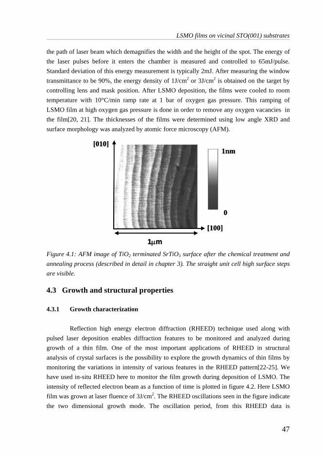
LSMO films on vicinal STO(001) substrates
47
the path of laser beam which demagnifies the width and the height of the spot. The energy of the laser pulses before it enters the chamber is measured and controlled to 65mJ/pulse. Standard deviation of this energy measurement is typically 2mJ. After measuring the window transmittance to be 90%, the energy density of 1J/cm2 or 3J/cm2 is obtained on the target by controlling lens and mask position. After LSMO deposition, the films were cooled to room temperature with 10°C/min ramp rate at 1 bar of oxygen gas pressure. This ramping of LSMO film at high oxygen gas pressure is done in order to remove any oxygen vacancies in the film[20, 21]. The thicknesses of the films were determined using low angle XRD and surface morphology was analyzed by atomic force microscopy (AFM).
Figure 4.1: AFM image of TiO2 terminated SrTiO3 surface after the chemical treatment and annealing process (described in detail in chapter 3). The straight unit cell high surface steps are visible. 4.3 Growth and structural properties 4.3.1 Growth characterization
Reflection high energy electron diffraction (RHEED) technique used along with pulsed laser deposition enables diffraction features to be monitored and analyzed during growth of a thin film. One of the most important applications of RHEED in structural analysis of crystal surfaces is the possibility to explore the growth dynamics of thin films by monitoring the variations in intensity of various features in the RHEED pattern[22-25]. We have used in-situ RHEED here to monitor the film growth during deposition of LSMO. The intensity of reflected electron beam as a function of time is plotted in figure 4.2. Here LSMO film was grown at laser fluence of 3J/cm2. The RHEED oscillations seen in the figure indicate the two dimensional growth mode. The oscillation period, from this RHEED data is
11µµmm
0
1nm[010]
[100]
11µµmm
0
1nm[010]
[100]

LSMO films on vicinal STO(001) substrates
48
determined to be 10 seconds. The oscillation intensity is found to be dropping rapidly which points out that the film surface becomes roughened as the growth proceeds. But the diffraction spots of island growth are not seen in the diffraction pattern after deposition. This means that the roughening during the growth is not that high enough to remove the steps on the film surface as later it is found in the AFM measurement that the films also shows vicinal steps on it’s surface.
0 50 100
20
40
60
80
100LSMO on STO
Inte
nsity
Time (seconds)
Before
After
a) b)
0 50 100
20
40
60
80
100LSMO on STO
Inte
nsity
Time (seconds)
Before
After
0 50 100
20
40
60
80
100LSMO on STO
Inte
nsity
Time (seconds)
Before
After
a) b)
Figure 4.2: a) RHEED intensity oscillations during the growth of LSMO film on TiO2 terminated STO substrate. b) Diffraction pattern of the sample taken along STO (100) direction at 0.35mbar before and after deposition respectively. 4.3.2 Surface morphology of LSMO film
Surface topography of LSMO films were analyzed by taking AFM images of its
surface. The surface morphology of LSMO films of different thicknesses (16nm, 26nm, 45nm and 21nm) is shown in figure 4.3. The films with thicknesses 16nm, 26nm and 45nm are grown with laser fluence of 1J/cm2 and the film with 21nm thickness was grown with laser fluence of 3J/cm2. These films, with thickness up to 85 nm, show atomically flat terraces separated by unit cell high steps. These AFM results indicate that the growth of LSMO on treated STO substrates is in two dimensional growth mode. Because the miscut angles and miscut directions of the substrates used are different, the surface step densities and step directions of each of these films are also different. The wavy steps which are seen in the film with thickness 26nm, is originated from the substrate itself because the treated substrate before depositing the film also had wavy steps.
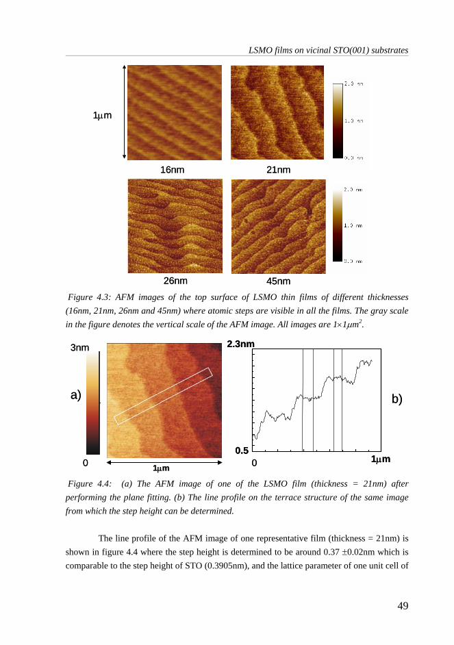
LSMO films on vicinal STO(001) substrates
49
Figure 4.3: AFM images of the top surface of LSMO thin films of different thicknesses (16nm, 21nm, 26nm and 45nm) where atomic steps are visible in all the films. The gray scale in the figure denotes the vertical scale of the AFM image. All images are 1×1µm2.
Figure 4.4: (a) The AFM image of one of the LSMO film (thickness = 21nm) after performing the plane fitting. (b) The line profile on the terrace structure of the same image from which the step height can be determined.
The line profile of the AFM image of one representative film (thickness = 21nm) is
shown in figure 4.4 where the step height is determined to be around 0.37 ±0.02nm which is comparable to the step height of STO (0.3905nm), and the lattice parameter of one unit cell of
16nm
26nm 45nm
21nm
1µm
16nm
26nm 45nm
21nm
1µm
11µµmm
2.3nm
0.51µm0
3nm
0
a) b)
11µµmm
2.3nm
0.51µm0
3nm
0
a) b)

LSMO films on vicinal STO(001) substrates
50
bulk LSMO (0.388nm). The above AFM results show that there is no obvious influence of laser fluence and thickness on the surface morphology of the film. 4.3.3 Structural analysis
The structural analysis of LSMO films was done using X-ray diffraction
measurements. The low angle XRD spectrum of one of the LSMO film is shown in figure 4.5 where the thickness is determined from the periodicity of oscillation of the XRD intensity. In section 3.3.2 of chapter 3, it is explained how film thickness can be determined from low angle XRD.
Figure 4.5: Low angle XRD of one of the representative LSMO film, from which the film thickness is derived.
We performed the 2theta XRD scan of films with varied thicknesses (21nm, 25nm and 80nm). In figure 4.6(a), the XRD spectrum of one of the LSMO film of thickness 80nm is shown where all the (00l) peaks can be seen. X-ray diffraction spectra (Zoomed in to (003) peak) of LSMO thin films of different thicknesses are given in figure 4.6(b) where Kα1 and Kα2 peaks are seen for both film and substrate. From these XRD spectrums, the out of plane lattice ‘c’ parameter of each LSMO film is determined and these values are found to be less than the bulk lattice parameter (0.388nm) of LSMO. The experimental out of plane lattice ‘c’ parameter value from (001), (002), (003) and (004) LSMO peaks (respective 2theta values = 23.11±0.25, 47.155±0.2, 73.87±0.2 and 106.4±0.2) was determined (using equation 3.1) to be 3.8456±0.041Å, 3.851±0.015Å, 3.8457±0.009Å, and 3.848±0.005Å respectively.
The reduction in the out of plane lattice ‘c’ parameter compared to bulk value can be explained with the lattice strain of LSMO thin films. The lattice mismatch of LSMO with STO substrate is found to be around 0.64% [(aSTO –aLSMO)/aSTO]. So there exists an in-plane tensile strain in the LSMO film.
1.0 1.5 2.0 2.5 3.0 3.5 4.010
100
1000
10000
100000
1000000
21nm
Inte
nsity
2θ

LSMO films on vicinal STO(001) substrates
51
Figure 4.6: (a) XRD spectrum of LSMO film of thickness 80nm. (b) X-ray diffraction spectra (Zoomed in to (003) peak.) of LSMO thin films of different thicknesses (shown in the legend). Here both STO (003) and LSMO (003) peaks are shown. The arrow in the figure indicates that the intensity decreases with decreasing thickness of LSMO films.
Earlier, Kawasaki et al[26] has already shown (Figure 4.7(a)) how the LSMO lattice get strained in both ‘a’ and ‘b’ in-plane directions in order to fit exactly on STO substrate lattice. LSMO lattice experiences in-plane tensile strain in this case. Cross section TEM micrograph of an LSMO film is also shown in figure 4.7(b) where it can be seen the perfect lattice fitting of LSMO on STO showing the epitaxial growth, confirming the above argument[27].
Figure 4.7: (a) Schematic picture showing the in-plane tensile strain of LSMO on STO substrate (only in-plane ‘a’ directions can be seen). Taken from Ref [26]. (b) Cross section TEM micrograph of LSMO film grown on STO substrate by Pulsed laser deposition. Taken from Ref[27]. Equal number (42 each) of lattice spacings for LSMO and STO are counted between the white lines as seen in figure.
LSMO (bulk)
a) b)
42 lattice spacings
42 lattice spacings
LSMO (bulk)LSMO (bulk)
a) b)
42 lattice spacings
42 lattice spacings
70 71 72 73 74 75 760.1
1
10
100
1000
10000
100000 21nm 29nm 80nm
LSMO (003)
STO (003)
Inte
nsity
2θ20 40 60 80 100 120
0.1
1
10
100
1000
10000
100000
1000000(001) (002)
(004)
(003)
Inte
nsity
2θa) b)
70 71 72 73 74 75 760.1
1
10
100
1000
10000
100000 21nm 29nm 80nm
LSMO (003)
STO (003)
Inte
nsity
2θ20 40 60 80 100 120
0.1
1
10
100
1000
10000
100000
1000000(001) (002)
(004)
(003)
Inte
nsity
2θ70 71 72 73 74 75 76
0.1
1
10
100
1000
10000
100000 21nm 29nm 80nm
LSMO (003)
STO (003)
Inte
nsity
2θ20 40 60 80 100 120
0.1
1
10
100
1000
10000
100000
1000000(001) (002)
(004)
(003)
Inte
nsity
2θ70 71 72 73 74 75 76
0.1
1
10
100
1000
10000
100000 21nm 29nm 80nm
LSMO (003)
STO (003)
Inte
nsity
2θ20 40 60 80 100 120
0.1
1
10
100
1000
10000
100000
1000000(001) (002)
(004)
(003)
Inte
nsity
2θa) b)

LSMO films on vicinal STO(001) substrates
52
The LSMO peaks are slightly broadened compared to the substrate peaks, which tell that the lattice parameter varies slightly at different regions of the film. We can note here that the peaks lies between the bulk (2theta value = 73.2) and the maximally strained position (2theta value = 74.5), and that with increasing thickness the gravity center of the peaks is not moving towards the bulk position (towards left). That means, as the thickness increases, the film is not getting relaxed in order to get the lattice parameter of its bulk value. From these results, we can conclude that the film is strained and the energy for straining is lower than the energy for forming dislocations. It is possible that while straining, oxygen vacancies in the lattice are created.
We have also used reciprocal space mapping to analyze the in-plane lattice matching of LSMO film with STO substrate. The plot (reciprocal space map) is a contour mapping of the peak intensity signal. In the maps, the ω and 2θ axes are converted in reciprocal lattice units. Figure 4.8 shows the results for two reciprocal space maps (hl scan and kl scan respectively) around the (202) and (022) reflection of an 80nm thick LSMO film. The reflections were chosen so that the in-plane lattice fitting could be analyzed. Here, the hl map shows that the peaks of both STO and LSMO layer have identical h values, indicating that the lattice ‘a’ parameter of both STO and LSMO are identical. In the kl map, the k values of both STO and LSMO are also found to be identical which indicates that the in-plane lattice ‘b’ parameters of both layer and substrate are identical as well.
Figure 4.8: (a) hl scan around the (202) reflection of 80 nm LSMO on STO. The h values of both STO and LSMO peaks are same (shown with a straight line in the figure). (b) kl scan around (022) reflection of the same film. The k values of both STO and LSMO peaks are same (shown with a straight line in the figure).
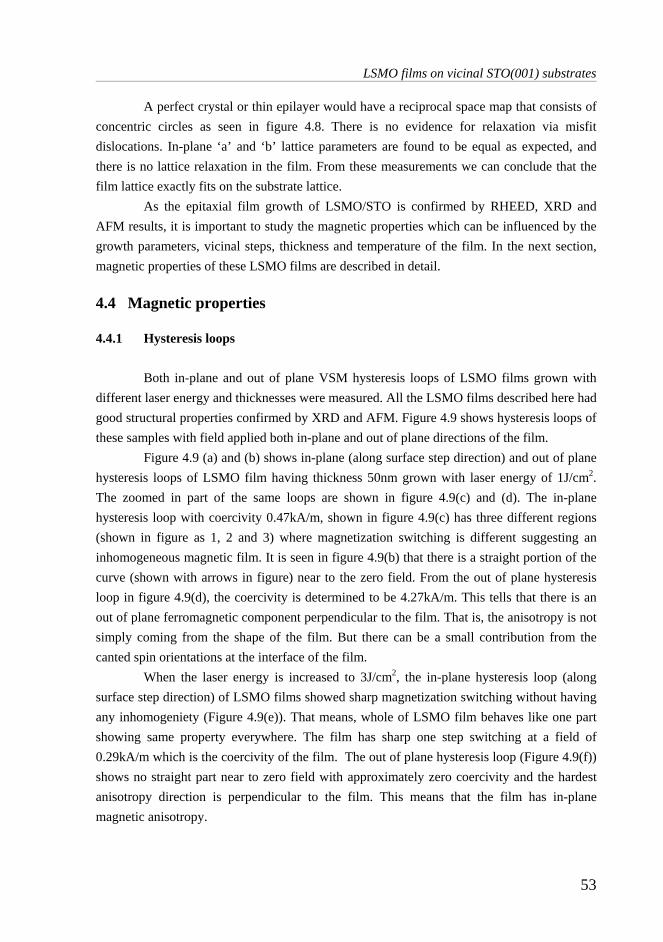
LSMO films on vicinal STO(001) substrates
53
A perfect crystal or thin epilayer would have a reciprocal space map that consists of concentric circles as seen in figure 4.8. There is no evidence for relaxation via misfit dislocations. In-plane ‘a’ and ‘b’ lattice parameters are found to be equal as expected, and there is no lattice relaxation in the film. From these measurements we can conclude that the film lattice exactly fits on the substrate lattice.
As the epitaxial film growth of LSMO/STO is confirmed by RHEED, XRD and AFM results, it is important to study the magnetic properties which can be influenced by the growth parameters, vicinal steps, thickness and temperature of the film. In the next section, magnetic properties of these LSMO films are described in detail.
4.4 Magnetic properties 4.4.1 Hysteresis loops Both in-plane and out of plane VSM hysteresis loops of LSMO films grown with different laser energy and thicknesses were measured. All the LSMO films described here had good structural properties confirmed by XRD and AFM. Figure 4.9 shows hysteresis loops of these samples with field applied both in-plane and out of plane directions of the film. Figure 4.9 (a) and (b) shows in-plane (along surface step direction) and out of plane hysteresis loops of LSMO film having thickness 50nm grown with laser energy of 1J/cm2. The zoomed in part of the same loops are shown in figure 4.9(c) and (d). The in-plane hysteresis loop with coercivity 0.47kA/m, shown in figure 4.9(c) has three different regions (shown in figure as 1, 2 and 3) where magnetization switching is different suggesting an inhomogeneous magnetic film. It is seen in figure 4.9(b) that there is a straight portion of the curve (shown with arrows in figure) near to the zero field. From the out of plane hysteresis loop in figure 4.9(d), the coercivity is determined to be 4.27kA/m. This tells that there is an out of plane ferromagnetic component perpendicular to the film. That is, the anisotropy is not simply coming from the shape of the film. But there can be a small contribution from the canted spin orientations at the interface of the film.
When the laser energy is increased to 3J/cm2, the in-plane hysteresis loop (along surface step direction) of LSMO films showed sharp magnetization switching without having any inhomogeniety (Figure 4.9(e)). That means, whole of LSMO film behaves like one part showing same property everywhere. The film has sharp one step switching at a field of 0.29kA/m which is the coercivity of the film. The out of plane hysteresis loop (Figure 4.9(f)) shows no straight part near to zero field with approximately zero coercivity and the hardest anisotropy direction is perpendicular to the film. This means that the film has in-plane magnetic anisotropy.

LSMO films on vicinal STO(001) substrates
54
Figure 4.9: (a) In-plane (along surface step direction) and (b) out of plane hysteresis loops of LSMO thin film of thickness 50nm grown with laser fluence 1J/cm2. The loops in (c) and (d) shows zoomed in part of the same hysteresis loops shown in (a) and (b) respectively. (e) In-plane (along surface step direction) and (f) out of plane hysteresis loops of LSMO thin film of thickness 40nm grown with laser fluence 3J/cm2.
-1000 -500 0 500 1000
-0.2
-0.1
0.0
0.1
0.2 Thickness = 50nmFluence = 1J/cm2
Mag
netic
mom
ent (µA
m2 )
H(kA/m)
-10 -5 0 5 10-0.4
-0.3
-0.2
-0.1
0.0
0.1
0.2
0.3
0.4Thickness = 40nmFluence = 3J/cm2
Mag
netic
mom
ent (µA
m2 )
H (kA/m)-1500 -1000 -500 0 500 1000 1500
-0.4
-0.3
-0.2
-0.1
0.0
0.1
0.2
0.3
0.4Thickness =40nmFluence =3J/cm2
Mag
netic
mom
ent (µA
m2 )
H (kA/m)
-60 -40 -20 0 20 40 60
-0.2
-0.1
0.0
0.1
0.2 Thickness = 50nmFluence = 1J/cm2
Mag
netic
mom
ent (µA
m2 )
H (kA/m)
⊥
⊥
//
//
c)
e) f)
1
23
-1000 -500 0 500 1000
-0.2
-0.1
0.0
0.1
0.2 Thickness = 50nmFluence = 1J/cm2
Mag
netic
mom
ent (µA
m2 )
H (kA/m)
//
⊥
a)
-60 -40 -20 0 20 40 60
-0.2
-0.1
0.0
0.1
0.2 Thickness = 50nmFluence = 1J/cm2
Mag
netic
mom
ent (µA
m2 )
H(kA/m)
b)
d)
-1000 -500 0 500 1000
-0.2
-0.1
0.0
0.1
0.2 Thickness = 50nmFluence = 1J/cm2
Mag
netic
mom
ent (µA
m2 )
H(kA/m)
-10 -5 0 5 10-0.4
-0.3
-0.2
-0.1
0.0
0.1
0.2
0.3
0.4Thickness = 40nmFluence = 3J/cm2
Mag
netic
mom
ent (µA
m2 )
H (kA/m)-1500 -1000 -500 0 500 1000 1500
-0.4
-0.3
-0.2
-0.1
0.0
0.1
0.2
0.3
0.4Thickness =40nmFluence =3J/cm2
Mag
netic
mom
ent (µA
m2 )
H (kA/m)
-60 -40 -20 0 20 40 60
-0.2
-0.1
0.0
0.1
0.2 Thickness = 50nmFluence = 1J/cm2
Mag
netic
mom
ent (µA
m2 )
H (kA/m)
⊥
⊥
//
//
c)
e) f)
1
23
-1000 -500 0 500 1000
-0.2
-0.1
0.0
0.1
0.2 Thickness = 50nmFluence = 1J/cm2
Mag
netic
mom
ent (µA
m2 )
H (kA/m)
//
⊥
a)
-60 -40 -20 0 20 40 60
-0.2
-0.1
0.0
0.1
0.2 Thickness = 50nmFluence = 1J/cm2
Mag
netic
mom
ent (µA
m2 )
H(kA/m)
b)
d)

LSMO films on vicinal STO(001) substrates
55
It is seen in the figure that saturation magnetic moment (0.16 µAm2) of 50nm LSMO film is lower than that of 40nm LSMO (0.3 µAm2) which can be due to the inhomogeniety of the film grown with lower fluence and it is explained in the next section. 4.4.2 Magnetization vs Temperature
The dependence of magnetization with temperature for LSMO films with three different deposition conditions (namely with laser fluence of 1J/cm2, 2J/cm2 and 3J/cm2) are plotted in figure 4.10. The thicknesses of these films were 26nm, 28nm and 21nm respectively. It is seen that the curie temperature is ~ 350K for all the films. That is, we could not find a noticeable change in TC with change in laser fluence. Here, a sharper ferromagnetic to paramagnetic transition can be seen in films grown with laser fluence of 2J/cm2 compared to films grown with laser fluence of 1J/cm2. The transition becomes even sharper when the fluence is increased to 3J/cm2. The magnetization value of this sample at 150K is 540kA/m which corresponds to the value of 3.08 Bohr magneton (µB) per manganese atom. The expected full saturation magnetization is 600kA/m (3.7µB) per manganese atom at 10K.
Figure 4.10: Temperature dependence of magnetization of LSMO thin films with thicknesses 21nm, 28nm and 26nm .grown with laser fluencies 3J/cm2, 2Jcm2 and 1J/cm2 respectively.
The broad transition of ferromagnetic to paramagnetic phase as seen in films grown
with lower laser fluence is because of the distribution of curie temperature (TC) of the LSMO at different areas of the film. The low values of magnetization of these films at 150K (~ 300kA/m and ~ 450 kA/m for films grown with laser fluence of 1J/cm2 and 2J/cm2 respectively) compared to the magnetization of films grown with laser fluence of 3J/cm2 and films prepared by other groups[15, 18], might be due to the oxygen deficiency in the film, as the laser energy used here is low. The films are grown more homogeneous when higher laser
150 200 250 300 350 400
0
100
200
300
400
500
600
3J/cm2
2J/cm2
1J/cm2
Mag
netiz
atio
n (k
A/m
)
Temperature (K)
LSMO films on vicinal STO(001) substrates
56
fluence is used. When material is ablated with higher laser fluence, its kinetic energy to reach the substrate is higher and the growth will be more stochiometric and epitaxial. This is the reason that the film grown with higher laser fluence 3J/cm2 has higher magnetization at lower temperature and sharp ferromagnetic to paramagnetic transition compared to other films grown with lower fluence.
Magnetic anisotropy measurements are performed only on LSMO films grown with laser energy of 3J/cm2 because these films were having better magnetic properties as explained above. More close analysis of the influence of substrate steps on magnetic anisotropy of our LSMO films of different thicknesses at different temperature are described in the next section.
4.4.3 Magnetic anisotropy
Magnetic anisotropy is produced through the interaction between spontaneous magnetization and the crystal lattice, so that the temperature dependence of spontaneous magnetization should give rise to a change in magnetic anisotropy. The magnetic anisotropy is also influenced by other factors such as thermal expansion of the lattice, thermal excitation of the electronic states of magnetic atoms, temperature dependence of valence states etc. More detailed general description about different kinds of magnetic anisotropy can be found in section 3.4.2 of chapter 3.
In-plane magnetic anisotropy behavior of LSMO films was characterized by vibrating sample magnetometer (VSM) at room temperature and 160 K. For each film, hysteresis loops were taken at different in-plane field directions with intervals of 5° field angle. Figure 4.11 shows two hysteresis loops obtained for a 25 nm thick LSMO film at room temperature, taken with applied field along 130° and 40° with respect to one edge of the substrate crystal [100] direction. These field directions were found to be the in-plane easy and hard directions, respectively. A clear difference in the remanence value can be seen. AFM measurements show that the film surface has steps which are a clear imprint of the treated STO substrate surface. Note that the step direction of each substrate is different because of the variation in miscut direction. A typical example of an AFM image of 25 nm thick film (the same sample explained in figure 4.11) is shown in the top panel of figure 4.12. The remanence of this film, taken from hysteresis loops at different field angles, versus in-plane field angle θ is also given in figure 4.12 (bottom panel).
Here θ is defined as angle between applied field direction and the [100] STO crystal direction. There is an oscillation with periodicity of 180° with highest remanence at θ ~ 130° and lowest remanence at θ ~ 37°. From this, we can conclude that this film has a uniaxial anisotropy with the easy direction along 130° and the hard direction along 37°. From the

LSMO films on vicinal STO(001) substrates
57
AFM image obtained from the same film, we found that the step direction is along the 133° ±5° direction, which corresponds with the easy axis, whereas the hard axis is perpendicular to the step direction (top panel of figure 4.12).
Figure 4.11: Magnetic hysteresis loops of a LSMO film of thickness 25 nm, with field applied in-plane along the easy axis (direction of 130° angle with respect to one crystal edge [100] of the substrate) and hard axis (direction of 40°) at room temperature.
Figure 4.12: Remanence vs in-plane field angle of a 25 nm thick LSMO film at room temperature (bottom panel) and the arrows here denote easy and hard directions. AFM image of the same film (top panel) with the step direction θ =133±5°. The gray scale range is from 0 to 2 nm.
-2.0 -1.5 -1.0 -0.5 0.0 0.5 1.0 1.5 2.0-0.15
-0.10
-0.05
0.00
0.05
0.10
0.15
T = 300KM
agne
tic m
omen
t (µA
m2 )
H (kA/m)
Hard axis (θ = 40°)
Easy axis (θ = 130°)
0 100 200
0.04
0.08
0.12
T = 300K
Easyθ ~ 130°
Hardθ ~ 37°
Rem
anen
ce (
µAm
2 )
Field angle (θ)
θ
2µm
[100]
[010]
0 100 200
0.04
0.08
0.12
T = 300K
Easyθ ~ 130°
Hardθ ~ 37°
Rem
anen
ce (
µAm
2 )
Field angle (θ)
θ
2µm
[100]
[010]

LSMO films on vicinal STO(001) substrates
58
Remanence versus field angle of the LSMO film with a thickness of 7 nm and a different step direction is given in figure. 4.13. Again, the remanence shows an oscillation with 180° periodicity. The highest remanence value was found at 100°±8°, whereas the lowest remanence is found in the 10° ±8° direction. This leads to the conclusion that this film also has a uniaxial anisotropy, with the easy axis along the 100° and the hard axis along the 10° direction. Once more, the easy axis of the uniaxial anisotropy in this film coincides with the step direction of the film as confirmed by the AFM image (step direction is 100°±5°) of the same film (top panel of figure. 4.13).
Figure 4.13: Remanence vs in-plane field angle of a 7 nm thick LSMO film at room temperature (bottom panel). Arrows denote easy and hard directions. AFM image of the same film (top panel) with the step direction θ =100±5°. The gray scale range is from 0 to 2 nm.
Subsequently, we have examined the anisotropy behavior of the films at low temperature (160 K). In 4.14(a), the remanence versus field angle at 160 K is plotted for the same film that is described in Figure. 4.11. Again the remanence oscillates with in-plane field angle. However, in contrast to the room temperature data, the remanence at 160 K oscillates with a periodicity of 90° with the highest value at 45° and lowest value at 0°. Here, the 45° and 0° are the [110] and [100] crystal directions which are the easy and hard axis, respectively. Hence, at low temperature the film has in-plane biaxial anisotropy instead of uniaxial anisotropy. In this case the easy and hard axes have no relation with the step
-100 -50 0 50 1000.00
0.01
0.02
0.03
T = 300K
Hardθ ~ 10°
Easyθ ~ 100°
Rem
anen
ce (
µAm
2 )
Field angle (θ)
θ
2µm
[100]
[010]
-100 -50 0 50 1000.00
0.01
0.02
0.03
T = 300K
Hardθ ~ 10°
Easyθ ~ 100°
Rem
anen
ce (
µAm
2 )
Field angle (θ)
θ
2µm
-100 -50 0 50 1000.00
0.01
0.02
0.03
T = 300K
Hardθ ~ 10°
Easyθ ~ 100°
Rem
anen
ce (
µAm
2 )
Field angle (θ)
θ
2µm
[100]
[010]
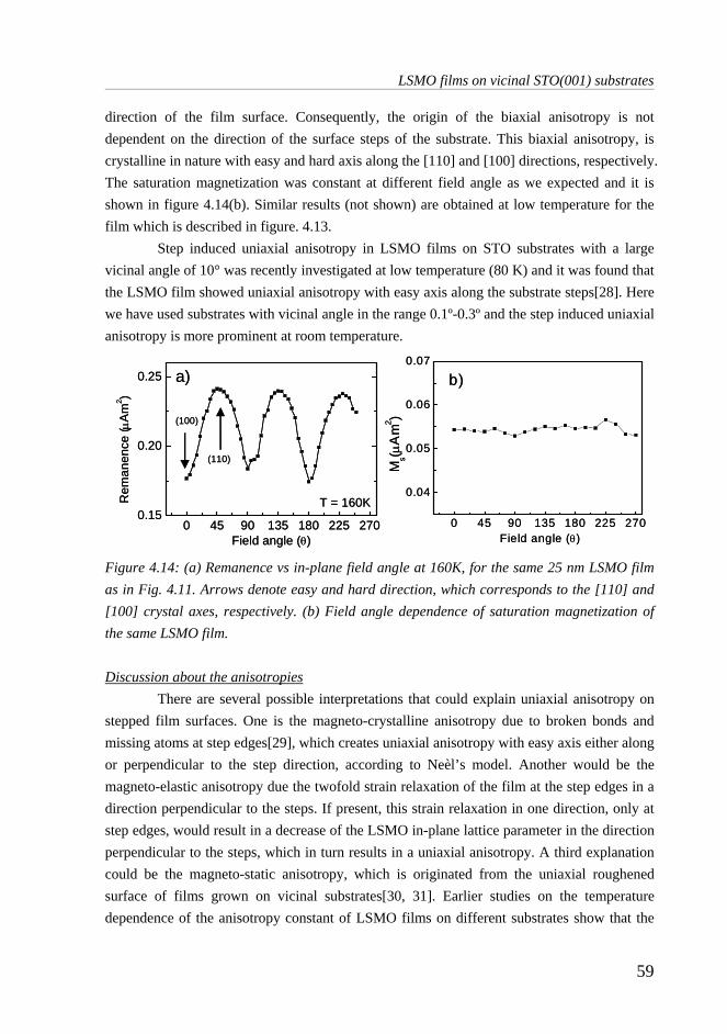
LSMO films on vicinal STO(001) substrates
59
direction of the film surface. Consequently, the origin of the biaxial anisotropy is not dependent on the direction of the surface steps of the substrate. This biaxial anisotropy, is crystalline in nature with easy and hard axis along the [110] and [100] directions, respectively. The saturation magnetization was constant at different field angle as we expected and it is shown in figure 4.14(b). Similar results (not shown) are obtained at low temperature for the film which is described in figure. 4.13.
Step induced uniaxial anisotropy in LSMO films on STO substrates with a large vicinal angle of 10° was recently investigated at low temperature (80 K) and it was found that the LSMO film showed uniaxial anisotropy with easy axis along the substrate steps[28]. Here we have used substrates with vicinal angle in the range 0.1º-0.3º and the step induced uniaxial anisotropy is more prominent at room temperature.
Figure 4.14: (a) Remanence vs in-plane field angle at 160K, for the same 25 nm LSMO film as in Fig. 4.11. Arrows denote easy and hard direction, which corresponds to the [110] and [100] crystal axes, respectively. (b) Field angle dependence of saturation magnetization of the same LSMO film.
Discussion about the anisotropies
There are several possible interpretations that could explain uniaxial anisotropy on stepped film surfaces. One is the magneto-crystalline anisotropy due to broken bonds and missing atoms at step edges[29], which creates uniaxial anisotropy with easy axis either along or perpendicular to the step direction, according to Neèl’s model. Another would be the magneto-elastic anisotropy due the twofold strain relaxation of the film at the step edges in a direction perpendicular to the steps. If present, this strain relaxation in one direction, only at step edges, would result in a decrease of the LSMO in-plane lattice parameter in the direction perpendicular to the steps, which in turn results in a uniaxial anisotropy. A third explanation could be the magneto-static anisotropy, which is originated from the uniaxial roughened surface of films grown on vicinal substrates[30, 31]. Earlier studies on the temperature dependence of the anisotropy constant of LSMO films on different substrates show that the
0 45 90 135 180 225 2700.15
0.20
0.25 a)
T = 160K
(110)
(100)
Rem
anen
ce (µ
Am
2 )
Field angle (θ)0 45 90 135 180 225 270
0.04
0.05
0.06
0.07
b)
Field angle (θ)
Ms(µ
Am
2 )
0 45 90 135 180 225 2700.15
0.20
0.25 a)
T = 160K
(110)
(100)
Rem
anen
ce (µ
Am
2 )
Field angle (θ)0 45 90 135 180 225 270
0.04
0.05
0.06
0.07
b)
Field angle (θ)
Ms(µ
Am
2 )
LSMO films on vicinal STO(001) substrates
60
strain induced by the substrates is not affecting the crystalline anisotropy constant[4]. As a consequence, we expect that the uniaxial strain at the step edges of the substrates is not affecting the anisotropy. In order to analyze more on the step induced magnetic anisotropy of these films, torque magnetometry at different temperatures are done and explained in next section. The biaxial anisotropy, which is dominating over uniaxial anisotropy at low temperatures, is determined by the fourfold crystalline anisotropy in the LSMO film on the STO substrate, which increases with decreasing temperature.
4.4.4 Analysis by torque Measurements
Magnetic torque measurement is a very powerful, quantitative, direct and straightforward technique to investigate the magnetic anisotropy (more details about the set up and measurement are described in section 3.4.2 of chapter 3). With this method, it is possible to establish the type of magnetic anisotropy, uniaxial or biaxial and to determine the orientation of the magnetic easy axis. The torque measurements were carried out on our LSMO/STO films in order to obtain more quantitative analysis of its anisotropies at different temperature. In these torque magnetometry measurements, a large rotating field is applied to the sample and the torque curve is plotted versus the field angle. This rotating field turns the magnetization within the (001) film plane. The anisotropy constants for each sample at different temperature can be determined by fourier analysis of the measured torque curves, neglecting any difference between magnetic field direction and magnetization direction. We focus here on the films of thickness 7nm, 18nm and 85nm respectively for most of the analysis to follow. LSMO films grow epitaxial, thereby replicating the step-terrace structure of the substrate up to the film surface, as confirmed by the atomic force microscopy images in figure 4.15. In these AFM images of the films, it is possible to see the direction of the terrace steps of each sample with respect to the edge of the sample. The sample edge direction is the [100] crystalline axis. So it is possible to determine how the terrace steps are oriented with respect to [100] crystal direction of the sample and they are 100º±5º, 90º±5 º, and 60º±5º angles for films with thickness 7nm, 18nm and 85nm respectively.
In order to measure the torque signal of LSMO thin films accurately, it was necessary to measure the background torque signal from holder and STO substrate so that those signal can be subtracted from the thin film torque curve. As the sample is having 5×5×1mm size, we used a Si disc (6×7×1mm) to place the sample on it so that it can fit well to the quartz sample holder. So, we have measured the torque curves of holder alone, holder + Si disc and holder + Si + STO substrate; at room temperature (Figure 4.16(a), (b) and(c) respectively). After measuring the torque curve of holder + Si + STO substrate, we rotated the STO substrate 90º in the plane and again the torque curve was plotted at room temperature

LSMO films on vicinal STO(001) substrates
61
(Figure 4.16 (d)). From this we conclude that the STO has a uniaxial torque contribution of not known origin.
Figure 4.15: AFM images of epitaxial LSMO films of thicknesses 7nm, 18nm, and 85nm respectively.
Figure 4.16: Torque curves (a) holder alone, (b) holder + Si, (c) holder + Si + STO(0º) and (d) holder + Si + STO (90º rotated) at room temperature.
2µm
7nm 85 nm18 nm[100]
θ
[100]
θ
[100]
θ
2µm
7nm 85 nm18 nm
2µm2µm
7nm 85 nm18 nm[100]
θ
[100]
θ
[100]
θ
0 100 200 300 400
-0.008
-0.004
0.000
0.004
0.008 Holder+Si+STO(900)
-Tor
que
(10 -7
Nm
)
Field angle (θ)
0 100 200 300 400
-0.005
0.000
0.005Holder +Si
-Tor
que
(10 -7
Nm
)
Field angle (θ)
0 100 200 300 400
-0.002
0.000
0.002Holder+Si+STO(00)
-Tor
que
(10 -7
Nm
)
Field angle (θ)
0 100 200 300 400
-0.001
0.000
0.001Quartz Holder
-Tor
que
(10 -7
Nm
)
Field angle (θ)a) b)
c) d)0 100 200 300 400
-0.008
-0.004
0.000
0.004
0.008 Holder+Si+STO(900)
-Tor
que
(10 -7
Nm
)
Field angle (θ)
0 100 200 300 400
-0.005
0.000
0.005Holder +Si
-Tor
que
(10 -7
Nm
)
Field angle (θ)
0 100 200 300 400
-0.002
0.000
0.002Holder+Si+STO(00)
-Tor
que
(10 -7
Nm
)
Field angle (θ)
0 100 200 300 400
-0.001
0.000
0.001Quartz Holder
-Tor
que
(10 -7
Nm
)
Field angle (θ)a) b)
c) d)

LSMO films on vicinal STO(001) substrates
62
When the torque curve is measured for holder + Si + STO at lower temperature of 20K, it is found that there is no notable change in the signal from that of room temperature torque signal. So we used only the room temperature data of (holder +Si + STO) for subtraction. As there is reasonable torque signal from the background, we have subtracted the signal of holder + Si + STO(either 0º or 90º) from all the film torque curves. It is found that the subtraction of holder + Si + STO(0º) works well for films of thickness 7nm and 18nm. But for film of thickness 85nm, the subtraction of holder + Si + STO(90º) works well. That is, the phase angles of uniaxial step induced anisotropy and biaxial crystalline anisotropy becomes correct when the above subtraction is performed. The torque curves of all the samples were taken for different temperatures and from each curve the corresponding subtraction of background signal was also performed. When the temperature increases above 200K, the torque signal of all the films becomes very close to that of background signal. So, the torque measurements shown here are only in the temperature range between 20K and 200K. In figure 4.17, the torque curves of all the three films are shown for 20K and 200K.
Figure 4.17: Torque curves of LSMO films of different thicknesses of (a) 7nm, (b) 18nm and (c) 85nm at 20K and 200K (shown in the legend of each figure).
0 100 200 300 400
-0.04
-0.02
0.00
0.02
0.04
18nm
-Tor
que
(10-7
Nm
)
Field angle (θ)
200K 20K
0 100 200 300 400
-0.08
-0.04
0.00
0.04
0.08 85nm
-Tor
que
(10-7
Nm
)
Field angle (θ)
200K 20K
0 100 200 300 400-0.02
-0.01
0.00
0.01
0.02
7nm
-Tor
que
(10-7
Nm
)
Field angle (θ-900)
200K 20K
a) b)
c)
0 100 200 300 400
-0.04
-0.02
0.00
0.02
0.04
18nm
-Tor
que
(10-7
Nm
)
Field angle (θ)
200K 20K
0 100 200 300 400
-0.08
-0.04
0.00
0.04
0.08 85nm
-Tor
que
(10-7
Nm
)
Field angle (θ)
200K 20K
0 100 200 300 400-0.02
-0.01
0.00
0.01
0.02
7nm
-Tor
que
(10-7
Nm
)
Field angle (θ-900)
200K 20K
a) b)
c)
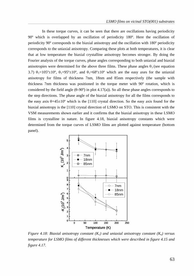
LSMO films on vicinal STO(001) substrates
63
In these torque curves, it can be seen that there are oscillations having periodicity 90º which is overlapped by an oscillation of periodicity 180º. Here the oscillation of periodicity 90º corresponds to the biaxial anisotropy and the oscillation with 180º periodicity corresponds to the uniaxial anisotropy. Comparing these plots at both temperatures, it is clear that at low temperature the biaxial crystalline anisotropy becomes stronger. By doing the Fourier analysis of the torque curves, phase angles corresponding to both uniaxial and biaxial anisotropies were determined for the above three films. These phase angles θ1 (see equation 3.7) θ1=105º±10º, θ1=95º±10º, and θ1=68º±10º which are the easy axes for the uniaxial anisotropy for films of thickness 7nm, 18nm and 85nm respectively (the sample with thickness 7nm thickness was positioned in the torque meter with 90º rotation, which is considered by the field angle (θ-90º) in plot 4.17(a)). So all these phase angles corresponds to the step directions. The phase angle of the biaxial anisotropy for all the films corresponds to the easy axis θ=45±10º which is the [110] crystal direction. So the easy axis found for the biaxial anisotropy is the [110] crystal direction of LSMO on STO. This is consistent with the VSM measurements shown earlier and it confirms that the biaxial anisotropy in these LSMO films is crystalline in nature. In figure 4.18, biaxial anisotropy constants which were determined from the torque curves of LSMO films are plotted against temperature (bottom panel).
Figure 4.18: Biaxial anisotropy constant (K1) and uniaxial anisotropy constant (Ku) versus temperature for LSMO films of different thicknesses which were described in figure 4.15 and figure 4.17.
0
1
2
3
4
5
Ku (
103 J
/m3 )
7nm 18nm 85nm
0 50 100 150 200 2500
1
2
3
4
5
6
7
8
9
-K1(1
03 J/m
3 )
Temperature (K)
7nm 18nm 85nm
0
1
2
3
4
5
Ku (
103 J
/m3 )
7nm 18nm 85nm
0 50 100 150 200 2500
1
2
3
4
5
6
7
8
9
-K1(1
03 J/m
3 )
Temperature (K)
7nm 18nm 85nm
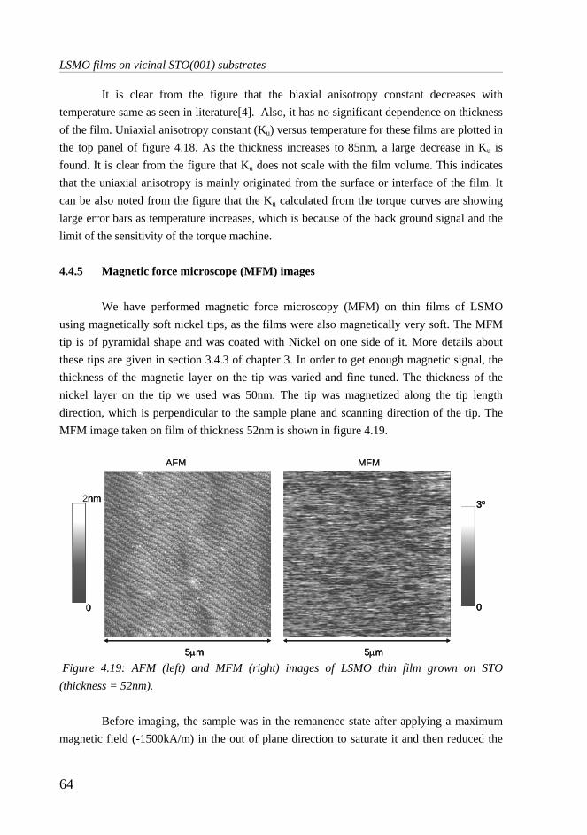
LSMO films on vicinal STO(001) substrates
64
It is clear from the figure that the biaxial anisotropy constant decreases with temperature same as seen in literature[4]. Also, it has no significant dependence on thickness of the film. Uniaxial anisotropy constant (Ku) versus temperature for these films are plotted in the top panel of figure 4.18. As the thickness increases to 85nm, a large decrease in Ku is found. It is clear from the figure that Ku does not scale with the film volume. This indicates that the uniaxial anisotropy is mainly originated from the surface or interface of the film. It can be also noted from the figure that the Ku calculated from the torque curves are showing large error bars as temperature increases, which is because of the back ground signal and the limit of the sensitivity of the torque machine. 4.4.5 Magnetic force microscope (MFM) images
We have performed magnetic force microscopy (MFM) on thin films of LSMO
using magnetically soft nickel tips, as the films were also magnetically very soft. The MFM tip is of pyramidal shape and was coated with Nickel on one side of it. More details about these tips are given in section 3.4.3 of chapter 3. In order to get enough magnetic signal, the thickness of the magnetic layer on the tip was varied and fine tuned. The thickness of the nickel layer on the tip we used was 50nm. The tip was magnetized along the tip length direction, which is perpendicular to the sample plane and scanning direction of the tip. The MFM image taken on film of thickness 52nm is shown in figure 4.19.
Figure 4.19: AFM (left) and MFM (right) images of LSMO thin film grown on STO (thickness = 52nm).
Before imaging, the sample was in the remanence state after applying a maximum magnetic field (-1500kA/m) in the out of plane direction to saturate it and then reduced the
5µm
0
3º
5µm
0
2nm
AFM MFM
5µm
0
3º
5µm
0
2nm
5µm
0
3º
5µm
0
2nm
AFM MFM

LSMO films on vicinal STO(001) substrates
65
field to zero. It can be seen that there is not much magnetic contrast which can be due to two reasons. One reason is that the film thickness of 52nm is not enough to give significant magnetic signal and the other is that Ni tip (as the tip is magnetically harder than the film) used is inducing the movement of domain walls along its scanning direction so that no magnetic signal is visible. These results are comparable with the MFM image of LSMO film grown on STO substrate, seen in literature[32]. 4.5 Conclusions
We have grown LSMO thin films on single crystalline STO substrates by pulsed laser deposition and optimized the deposition conditions such that the film grows epitaxial and shows high quality structural and magnetic properties. The XRD, RHEED and AFM measurements shows that the film grows in two dimensional or layer by layer growth mode resulting in a vicinal film surface, with unit cell high steps even up to film thickness of 85nm. It is observed that the LSMO film experiences an in-plane tensile strain so that the out of plane lattice parameter of LSMO is decreased to make the volume of the unit cell constant. Lattice parameters extracted from both 2 theta and reciprocal space mapping measurements confirms that LSMO lattice exactly fits on the STO lattice and the in-plane lattice parameters of LSMO are equal to that of STO. That is, high quality single crystalline LSMO film has been grown and has perfect lattice fitting with the STO substrate.
Magnetic measurements carried out by vibrating sample magnetometry show that the film has in-plane magnetic anisotropy. More extensive studies on this in-plane anisotropy of these films reveal a mixture of both biaxial and uniaxial in-plane anisotropy which were due to the crystalline nature of the film and the vicinal steps on the film surface respectively. It is observed that step induced uniaxial anisotropy is more prominent at room temperature and biaxial crystalline anisotropy is more prominent at low temperature. Torque measurements were carried out to extract biaxial and uniaxial anisotropy directions and quantify the anisotropy constants at different temperature. The uniaxial anisotropy axes correspond to the surface step direction and biaxial anisotropy axes corresponds to the crystalline directions of the film. From the background measurements, it is concluded that STO substrate has a small uniaxial anisotropy. The dependence of both biaxial and uniaxial anisotropy constants on temperature was studied and the results show that the biaxial crystalline anisotropy constant (K1) decreases with temperature and it has no dependence on the film thickness. As uniaxial anisotropy constant (Ku) does not scale with volume of the film, it can be concluded that the step induced uniaxial anisotropy is mainly originated from the surface or interface of the film.
LSMO films on vicinal STO(001) substrates
66
In comparison to the earlier studies on magnetic anisotropy of LSMO films, interestingly, we have observed uniaxial step induced anisotropy which can be due to the high quality thin film growth on chemically treated substrate having vicinal surface steps. Also, the films which were studied here were comparatively thin (below 100nm) and this gives strong contribution from the interface or/and surface steps of the film. The competition between step-induced uniaxial anisotropy and biaxial crystalline anisotropy can play an important role in the performance of devices made from LSMO, operating at room temperature. 4.6 References 1. M.-H. Jo, N. D. Mathur, N. K. Todd and M. G. Blamire, Very large
magnetoresistance and coherent switching in half-metallic manganite tunnel junctions. Physical Review B, 2000. 61(22): p. R14905.
2. M. Bowen, M. Bibes, A. Barthelemy, J. P. Contour, A. Anane, Y. Lemaitre and A. Fert, Nearly total spin polarization in La2/3Sr1/3MnO3 from tunneling experiments. Applied Physics Letters, 2003. 82(2): p. 233-235.
3. J. M. De Teresa, A. Barthélémy, A. Fert, J. P. Contour, R. Lyonnet, F. Montaigne, P. Seneor and A. Vaurès, Inverse Tunnel Magnetoresistance in Co/SrTiO3/La0.7Sr0.3MnO3: New Ideas on Spin-Polarized Tunneling. Physical Review Letters, 1999. 82(21): p. 4288.
4. K. Steenbeck and R. Hiergeist, Magnetic anisotropy of ferromagnetic La0.7(Sr, Ca)0.3MnO3 epitaxial films. Applied Physics Letters, 1999. 75(12): p. 1778-1780.
5. A-M Haghiri-Gosnet and J-P Renard, CMR manganites: physics, thin films and devices. Journal of physics D: Applied physics, 2003. 36: p. R127-R150.
6. M.C. Robson C. Kwon, K.-C. Kim, J.Y. Gu, S.E. Lofland,S.M. Bhagat, Z. Trajanovic, M. Rajeswari, T. Venkatesan, and R.D. Gomez A.R. Kratz, R. Ramesh, Stress-induced effects in epitaxial (La0.7Sr0.3)MnO3 films. Journal of Magnetism and Magnetic Materials, 1997. 172: p. 229-236.
7. N. M. Souza-Neto, A. Y. Ramos, H. C. N. Tolentino, E. Favre-Nicolin and L. Ranno, Local anisotropy in strained manganite thin films. Applied Physics Letters, 2003. 83(17): p. 3587-3589.
8. M. Rajeswari, R. Shreekala, A. Goyal, S. E. Lofland, S. M. Bhagat, K. Ghosh, R. P. Sharma, R. L. Greene, R. Ramesh, T. Venkatesan, and T. Boettcher, Correlation between magnetic homogeneity, oxygen content, and electrical and magnetic properties of perovskite manganite thin films. Applied Physics Letters, 1998. 73(18): p. 2672-2674.
9. F. Tsui, M. C. Smoak, T. K. Nath and C. B. Eom, Strain-dependent magnetic phase diagram of epitaxial La0.67Sr0.33MnO3 thin films. Applied Physics Letters, 2000. 76(17): p. 2421-2423.
10. Y. Suzuki, H. Y. Hwang, S. W. Cheong and R. B. van Dover, The role of strain in magnetic anisotropy of manganite thin films. Applied Physics Letters, 1997. 71(1): p. 140-142.
11. Y. Suzuki, H. Y. Hwang, S. W. Cheong, T. Siegrist, R. B. van Dover, A. Asamitsu and Y. Tokura, Magnetic anisotropy of doped manganite thin films and crystals. Journal of Applied Physics, 1998. 83: p. 7064-7066.

LSMO films on vicinal STO(001) substrates
67
12. J.J. Harris, B. A. Joyce and and P. J. Dobson, Oscillations in the surface structure of &doped GaAs during growth by MBE. Surface Science 1981. 103: p. L90-L96.
13. C. E. C. Wood, RED intensity oscillations during MBE of GaAs. Surface Science, 1981. 108(2): p. L441-L443.
14. M. Lippmaa, N. Nakagawa, M. Kawasaki, S. Ohashi and H. Koinuma, Growth mode mapping of SrTiO3 epitaxy. Applied Physics Letters, 2000. 76(17): p. 2439-2441.
15. A. M. Haghiri-Gosnet, J. Wolfman, B. Mercey, Simon Ch, P. Lecoeur, M. Korzenski, M. Hervieu, R. Desfeux and G. Baldinozzi, Microstructure and magnetic properties of strained La0.7Sr0.3MnO3 thin films. Journal of Applied Physics, 2000. 88(7): p. 4257-4264.
16. M. Koubaa, A. M. Haghiri-Gosnet, R. Desfeux, Lecoeur Ph, W. Prellier and B. Mercey, Crystallinity, surface morphology, and magnetic properties of La0.7Sr0.3MnO3]thin films: An approach based on the laser ablation plume range models. Journal of Applied Physics, 2003. 93(9): p. 5227-5235.
17. M. Bibes, B. Martinez, J. Fontcuberta, V. Trtik, C. Ferrater, F. Sanchez, M. Varela, R. Hiergeist and K. Steenbeck, Anisotropic magnetoresistance of (0 0 h), (0 h h) and (h h h)La2/3Sr1/3MnO3 thin films on (0 0 1) Si substrates. Journal of Magnetism and Magnetic Materials 2000. 211: p. 206-211.
18. P. Lecoeur, P. L. Trouilloud, Xiao Gang, A. Gupta, G. Q. Gong and X. W. Li, Magnetic domain structures of La 0.67Sr0.33MnO3 thin films with different morphologies. Journal of Applied Physics, 1997. 82(8): p. 3934-3939.
19. Koster Gertjan, L. Kropman Boike, J. H. M. Rijnders Guus, H. A. Blank Dave and Rogalla Horst, Quasi-ideal strontium titanate crystal surfaces through formation of strontium hydroxide. Applied Physics Letters, 1998. 73(20): p. 2920-2922.
20. R. Cauro, A. Gilabert, J. P. Contour, R. Lyonnet, M. G. Medici, J. C. Grenet, C. Leighton and Ivan K. Schuller, Persistent and transient photoconductivity in oxygen-deficient La2/3Sr1/3MnO3-δ thin films. Physical Review B, 2001. 63(17): p. 174423.
21. D. Joonghoe, N. H. Hur, I. S. Kim and Y. K. Park, Oxygen pressure and thickness dependent lattice strain in La0.7Sr0.3MnO3 films. Journal of Applied Physics, 2003. 94(12): p. 7670-7674.
22. D. H. A. Blank , G. J. H. M. Rijnders, G. Koster and H. Rogalla, In-situ monitoring during pulsed laser deposition using RHEED at high pressure. Applied Surface Science 1998. 127-129: p. 633-638.
23. S. Cho, A. DiVenere, G. K. Wong, J. B. Ketterson, J. R. Meyer and J.-I. Hong, Growth-mode modification of Bi on CdTe(111)A using Te monolayer deposition. Physical Review B, 1998. 58(4): p. 2324.
24. D. H. A. Blank, G. Koster, G. A. J. H. M. Rijnders, E. van Setten, P. Slycke and and H. Rogalla, Epitaxial growth of oxides with pulsed laser interval deposition. Journal of Crystal Growth, 2000. 211: p. 98-105.
25. G. J. H. M. Rijnders, G. Koster, D. H. A. Blank and H. Rogalla, In situ monitoring during pulsed laser deposition of complex oxides using reflection high energy electron diffraction under high oxygen pressure. Applied Physics Letters, 1997. 70(14): p. 1888-1890.
26. M. Kawasaki, M. Izumi, Y. Konishi, T. Manako and and Y. Tokura, Perfect epitaxy of perovskite manganite for oxide spin-electronics. Materials science and Engineering B, 1999. 63(1-2): p. 49-57.
27. F. M. Postma, R. Ramaneti, T. Banerjee, H. Gokcan, E. Haq, D. H. A. Blank, R. Jansen and J. C. Lodder, Epitaxial diodes of a half-metallic ferromagnet on an oxide semiconductor. Journal of Applied Physics, 2004. 95: p. 7324-7326.

LSMO films on vicinal STO(001) substrates
68
28. Wang Zhi-Hong, G. Cristiani and H. U. Habermeier, Uniaxial magnetic anisotropy and magnetic switching in La0.67Sr0.33MnO3 thin films grown on vicinal SrTiO3(100). Applied Physics Letters, 2003. 82(21): p. 3731-3733.
29. D. S. Chuang, C. A. Ballentine and R. C. O'Handley, Surface and step magnetic anisotropy. Physical Review B, 1994. 49(21): p. 15084.
30. Rodrigo Arias and D. L. Mills, Theory of roughness-induced anisotropy in ferromagnetic films: The dipolar mechanism. Physical Review B, 1999. 59(18): p. 11871.
31. A. Encinas-Oropesa and F. N. V. Dau Origin of magnetic anisotropy in thin films deposited on step-bunched substrates. Journal of Magnetism and Magnetic Materials, 2003. 256: p. 301-305.
32. D. Joonghoe, Y. N. Kim, Y. S. Hwang, J. C. Kim and N. H. Hur, Strain-induced magnetic stripe domains in La0.7Sr0.3MnO3 thin films. Applied Physics Letters, 2003. 82(9): p. 1434-1436.

Chapter 5
La0.67Sr0.33MnO3 films on NdGaO3 substrates
Epitaxial La0.67Sr0.33MnO3 thin films are grown on vicinal, NdGaO3 substrates of different orientations and their structural and magnetic properties are investigated. The influence of strain state and growth geometry of LSMO film on its magnetic properties was analyzed at different temperatures. Magnetization reversal mechanism of LSMO/NGO(100) was also studied using angle dependent coercivity measurements.
5.1 Introduction
The dependence of magnetic properties, especially magnetic anisotropy on the strain state in the film can be analyzed by growing La0.67Sr0.33MnO3 (LSMO) on substrates having different lattice mismatch with the film. LSMO grown on SrTiO3 (STO) substrate have in-plane magnetic anisotropy (magnetic axis with in-plane easy axis) which is the combination of uniaxial step induced anisotropy and biaxial crystalline anisotropy as depicted earlier in chapter 4. It is interesting to analyze the magnetic anisotropy of LSMO film grown on neodymium gallate, (NdGaO3) substrate as the film has a different strain state on this substrate compared to that of STO. NdGaO3 (NGO) is widely used as substrate material for high-temperature superconductors (HTSC) and colossal magnetoresistive (CMR) materials, because it has the low mismatch between film and substrate lattice, both at the deposition and application temperatures [1-8]. This substrate is orthorhombic (space group Pbnm) with a = 5.43 Å, b = 5.50 Å and c = 7.71 Å [9-11]. LSMO on NGO(110) experiences an in-plane uniaxial compressive strain in which only one in-plane lattice parameter is significantly different[11, 12]. Researchers have found magnetic stripe domains with almost straight line shape in LSMO film grown on NGO(110) and the stripe domain ordering can be readily

La0.67Sr0.33MnO3 films on NdGaO3 substrates
70
controlled by the external magnetic field[12, 13]. Some other studies on LSMO films grown on NGO(110) shows 'feather' like magnetic contrast in magnetic force microscopy (MFM) images which is characteristic of films with in-plane magnetic anisotropy[9]. Here the shape of the magnetic pattern was fully correlated with the magnetic easy axis of the film. As described in previous chapter, the magnetic anisotropy axes of LSMO film can be tuned by selecting the vicinal steps in a desired direction on the STO substrate at room temperature. In this chapter, we have studied the influence of vicinal steps and temperature on magnetic anisotropy of LSMO films on NGO substrates of different orientations as little is known in this subject.
Here we have investigated the influence of growth and substrate orientations on magnetic properties of LSMO film on NGO. In section 5.2, growth and structural properties of LSMO film on NGO substrates of different orientations are described using the experimental tools like XRD, RHEED, and AFM. Magnetic studies of these films are shown in section 5.3 where a more elaborate description of magnetic properties like magnetic anisotropy, magnetization versus temperature, magnetization reversal mechanism and magnetic domain imaging by MFM etc. can be found.
5.2 Growth and structural properties
LSMO thin films were grown on NGO substrates by pulsed laser deposition (PLD). Here we have used mainly three different orientations of NGO substrates namely NGO(100)o, NGO(110)o and NGO(001)o respectively. The subscript ‘o’ represents the orthorhombic metric. 5.2.1 Crystal structure of NdGaO3 (NGO)
NdGaO3 has, at room temperature, a GdFeO3 type structure (space group Pbnm) [14].
Among the lanthanide gallates, it is the only oxide with no structural phase transitions in the temperature range 12-1773K[15]. As NGO substrates of different orientations offer various in-plane strain states, LSMO films grown on it not only have change in its structural and magnetic properties but it can also have different growth behavior. Orthorhombic crystal structure of NGO is shown in figure 5.1, where the (100)o (110) and (001)o planes are indicated in figure 5.2(a) (b) and (c) respectively.
The NGO structure can also be described in the pseudocubic space group, in which the [100] pseudocubic direction corresponds to the [110] orthorhombic direction, and the average pseudocubic lattice parameter, a1, is related to the orthorhombic unit cell by a ~ √2 a1, b ~ √ 2 a1, and c ~ 2 a1. In figure 5.1, it can be clearly seen that both Nd and Ga atoms are

La0.67Sr0.33MnO3 films on NdGaO3 substrates
71
present in (100)o NGO planes where as, either Nd or Ga atoms are only present in (110)o and (001)o NGO planes.
Figure 5.1: Crystal structure of NdGaO3 (orthorhombic) where the (100) plane (a), (110)o plane (b) and (001)o (c) are indicated. NGO(100)o
NGO(100)o orientation is first taken into consideration in order to analyze how the LSMO lattice fits on the NGO (100)o plane. In figure 5.2(a) top view of NGO (100)o plane is depicted on which diagonal plane of LSMO fits well. Top view of the diagonal plane of LSMO fitting on (100)o plane of NGO and the side view of the substrate lattice and LSMO is schematically shown in figure 5.2(b) and (c) respectively. LSMO lattice on NGO(100)o has its unit cell diagonal rotated out of plane so that it has good lattice match with the lattice ‘a’ parameter of NGO which is 5.43 Å. Here the step height of the substrate is half of the lattice ‘a’ parameter which then is 2.75 Å (Figure 5.2(c)).
There is uniaxial tensile strain in the direction of lattice ‘b’ axis and compressive strain in the direction of lattice ‘c’ axis of NGO(100)o . The lattice mismatch of the film, calculated from the lattice parameters of both NGO and LSMO are -0.23% in the direction of NGO lattice ‘b’ axis ([010]) and 0.64% in the direction of NGO lattice ‘c’ axis ([001]). As the strains are unequal, it is expected to get uniaxial in-plane magnetic anisotropy in LSMO films on these substrates. More details about the values of lattice strains along the crystal directions of both NGO substrates and LSMO film are given in Table 5.1 and Table 5.2 respectively. From the above described crystal lattice fitting, it is found that there is no separate La(Sr)O

La0.67Sr0.33MnO3 films on NdGaO3 substrates
72
and MnO2 terminations as shown in figure 2.1 in chapter 2. Instead, the terminating layers will have both Mn and La(Sr) atoms or only oxygen atoms.
Figure 5.2: (a) Top view of (100)o plane of NGO substrate. b) Top view of the diagonal plane of LSMO which is superimposed on NGO (100)o plane. c) Side view of the (100)o NGO substrate and LSMO lattice which grows on it. LSMO lattice orientations [(001)o, (110)o , and (100)o ] are also shown. Substrate treatment of NGO(100)o
Earlier, Ohnishi et al. have shown that an A-site (i.e., NdO1+x) single terminated (001)o NdGaO3 surface can be obtained after 2h annealing in air at high temperature (1000°C), as demonstrated by coaxial impact-collision ion scattering spectroscopy (CAICISS) measurements[16].
Here, NGO(100)o substrates are thermally treated before the deposition of LSMO. It is already seen that the lattice planes in the out of plane direction of this substrate are either consisting of Nd and Ga atoms or only oxygen atoms. So, there is no significance of a chemical treatment to get one termination on the surface. So this substrate requires only the annealing process to get good straight vicinal steps on its surface. We annealed this substrate at 950ºC for 1 hour in oxygen flow of 1 bar of oxygen. AFM image of the annealed substrate is shown in figure 5.3. The step height here determined to be equal to 0.27 ±0.02 nm.
The step height of NGO(100)o determined from the AFM experiment (0.27±0.02nm) match with the step height found from the lattice structure drawings (0.272nm) which is being described in the previous paragraphs. The annealed substrates are comparatively smooth and clean having atomic steps which will be very suitable template for growing epitaxial LSMO film on it.

La0.67Sr0.33MnO3 films on NdGaO3 substrates
73
Figure 5.3: (a) AFM image of NGO (100)o after annealing 1 hour at 950°C in oxygen flow of
200 ml/hour. b) The line profile of the substrate from which the step height can be determined.
Table 5.1: Lattice mismatch of the film on NGO substrates of (100)o , (110)o , (001)o and (010)o orientations in the in-plane substrate crystal directions.
Lattice mismatch in the in-plane directions NGO (100)o
NGO (110)o
NGO (001)o
NGO (010)o
Along in-plane substrate (100)o axis - -
1% 1%
Along in-plane substrate (001)o axis 0.64% 0.64% - 0.64%
Along in-plane substrate (110)o axis - 0.38%
- -
Along in-plane substrate (010)o axis -0.23%
- -0.23% -
Table 5.2: Lattice mismatch of the film on NGO substrates of (100)o , (110)o , (001)o and (010)o orientations in the crystal directions of LSMO film.
Lattice mismatch in the in-plane directions NGO (100)o
NGO (110)o
NGO (001)o
NGO (010)o
Along LSMO (100)o axis 0.40% 0.38% 0.27% 0.4%
Along LSMO (001)o axis 0.40% 0.64% - 0.4%
Along LSMO (110)o axis 0.23% 0.35% 1% 1%
Along LSMO (010)o axis - 0.27%
1µm
1nm
0
1.1nm
0
a) b)
800nm1µm
1nm
0
1.1nm
0
a) b)
800nm

La0.67Sr0.33MnO3 films on NdGaO3 substrates
74
NGO (110)o
Earlier, it has been studied how Sodium doped-Lanthanum manganate thin films can be deposited on NGO(110)o substrates which gives a different growth template compared to NGO(100)o [11]. Also, there are reports on magnetic properties of LSMO films grown on these substrates[12]. The crystal lattice planes of this substrate on which LSMO grows can be seen in figure 5.4. There can be two terminations on the surface of the substrate, either NdO1+δ or GaO2- δ which are shown in figure 5.4 (a) and (b) respectively.
Figure 5.4: Possible termination layers of NGO (110)o , namely (a) NdO1+δ and (b) GaO2- δ.
In figure 5.5 it is shown how LSMO lattice fits on this NGO (110)o lattice which was terminated with GaO2-δ layer. Figure 5.5(a) shows the top view of the GaO2-δ terminated layer and (b) describes how the LSMO cubic lattice fits well on top of this layer. In figure 5.5 (c), we can also see the schematic of the side view where the substrate and film lattices are shown. Using the LSMO and NGO lattice parameters lattice mismatch of the film is calculated and it is found that there is uniaxial compressive strain in the direction of lattice ‘c’ axis of NGO (110)o and it is calculated to be 0.64% in this direction. Also there is compressive strain perpendicular to this direction and the lattice mismatch in this direction is 0.38%. So it is expected to get uniaxial in-plane magnetic anisotropy in LSMO films on these substrates also with easy or hard axis in the direction of ‘c’ axis of NGO. These NGO substrates we have used were cut in 55º angle from one of the crystal direction (‘c’ axis of NGO). So one of the in-plane crystal direction was ~55º away from one edge of the substrate. NGO (001)o
In figure 5.6, it is depicted how LSMO lattice can be fitted on GaO2-δ terminated surface of NGO (001)o. Schematic picture of the top view of (001)o plane of NGO is shown in

La0.67Sr0.33MnO3 films on NdGaO3 substrates
75
figure 5.6(a) and figure 5.6(b) shows the top view of 45º rotated (in-plane) crystal plane of LSMO which fits well on the (001)o plane of NGO (figure 5.6(c)). Here the lattice mismatch is compressive (1.0%) in the direction of lattice ‘a’ axis of NGO and tensile (-0.23%) in the direction of lattice ‘b’ axis of NGO. So we expect a strong in-plane uniaxial magnetic anisotropy in LSMO film grown on this substrate. In here, when the film grows on the substrate, the film crystal lattice get 45º rotated in in-plane with respect to the substrate lattice as seen in figure 5.6(b).
Figure 5.5: a) Top view of the GaO2- δ terminated layer of NGO (110)o plane and b) top view
of this plane of NGO substrate on which the cubic LSMO lattice has been superimposed. c)
Side view of the (110)o NGO substrate and LSMO lattice which grows on it.
Figure 5.6: (a) Top view of the GaO2- δ terminated layer of NGO (001)o plane and b) top view
of this plane of NGO substrate on which the cubic LSMO lattice fits well. c) Side view of the
(001)o NGO substrate and LSMO lattice which grows on it.

La0.67Sr0.33MnO3 films on NdGaO3 substrates
76
NGO(110)o and NGO(001)o substrates, which have two terminations on its surface have treatment method different from that of NGO(100)o . In order to get single terminated growth surface, the substrate (NGO(110)o or NGO(001)o) was chemically treated to remove selectively one of the surface oxide layers (the one with base character, ie, NdO2-x)[17]. Chemical etching is based on the fact that the substrate has the layered structure and there is a difference in chemical reactivity of the constituent oxides. The etching experiments were done at room temperature, in an ultrasonic bath using a modified commercial BHF solution. The commercial available BHF solution (12.5 vol% HF + 87.5 vol% NH4F) used for SrTiO3 etching was modified for the purpose of this work. As the surface energy of NGO(110)o and NGO(001)o are different, their chemical treatment had to be done in solutions with different pH values, higher for former and lower for latter, respectively. For NGO(110)o , the etching solution consisted of 10 ml commercial BHF + 4 ml NH4OH (37 vol%) + 90 ml deionised water. The resulted solution has a pH = 5.0-5.5. For (001)oNdGaO3, the etching solution consisted of 20 ml commercial BHF + 3 ml NH4OH (37 vol%) + 110 ml deionised water and the pH was resulted to be 4-4.5[17].
In the etching procedure, first the substrates were soaked in deionised water for 30 minutes, in ultrasonic bath leading to hydroxide [Nd(OH)3.xH2O] formation at the surface. Then the etching was done by the modified BHF for 0.5-2 minutes followed by annealing at 950ºC-1000ºC for 1-2 hour in O2 pressure of 1 bar to facilitate surface recrystallisation. The AFM images of treated NGO(110)o and NGO(001)o substrates are given in figure 5.7. NGO(001)o substrates were chemically etched for 30 seconds in the modified BHF solution (pH =4-4.5) and annealed at 950ºC for 1 hour in O2 pressure of 1 bar(figure 5.7(a)). Here the substrates steps were not straightened up and there were still unitcell high islands on the terraces. These substrates are needed to be annealed at higher temperature. So we have chemically treated the substrate and annealed it at 1000ºC for 2 hour in O2 pressure of 1 bar. Then the substrate found to show very clear smooth steps of unitcell height (figure 5.7(b)) equal to ~ 0.4nm.
NGO(110)o substrate was annealed at 950ºC for 1 hour in O2 pressure of 1 bar, and the AFM image (fig 5.7(c)) of it shows very clear unitcell high surface steps. Neverthless, there are surface defects on the terraces probably formed because of the surface decomposition. When this substrate was chemically etched for 30 seconds and annealed at 950ºC for 1 hour in O2 pressure of 1 bar, the surface looks smooth having unitcell high steps and there is no surface defects found in it (fig 5.7(d)). So, we have used only the NGO substrates that were described in figure 5.7(b) and (d) for LSMO depositions which will be described later in this chapter. It can be noted that the step density in NGO(110)o and NGO(001)o substrates are different and this attributes to the difference in miscut angles of these NGO(001)o and NGO(110)o substrates which are ~ 0.03 and ~0.14 respectively.

La0.67Sr0.33MnO3 films on NdGaO3 substrates
77
Figure 5.7: The AFM images of NGO (001)o, (a) chemically etched for 30s and annealed at 950°C for 1 hour in O2 pressure of 1 bar (b) chemically etched for 2 minutes and annealed at 1000°C for 2 hour in O2 pressure of 1 bar. (c) AFM images of NGO (110)o which is only annealed for 1 hour in O2 pressure of 1 bar and (d) chemically etched for 30 seconds and annealed at O2 pressure of 1 bar. In the zoomed image shown in inset of (c) the surface defects (encircled) are visible and not in inset of (d). 5.2.2 Growth and surface analysis
By monitoring the variations of Reflection high energy electron diffraction
(RHEED) intensity taken during the growth of LSMO on different NGO substrates, the film growth dynamics can be comprehensively studied. The intensity of RHEED features shows an oscillatory behavior, which is directly related to the growth rate. It is seen that there occurs RHEED oscillations for films grown on NGO substrates of different orientations, which damp out with the time of deposition (Figure 5.8, Figure 5.9, and Figure 5.10). Nevertheless,
5µma)
d)c)
b) 5µm
2µm 2µm
5µma)
d)c)
b) 5µm
2µm 2µm

La0.67Sr0.33MnO3 films on NdGaO3 substrates
78
the RHEED diffraction patterns of each sample after deposition shows that the diffraction spots are still present which has become slightly streaky and there is no other diffraction spots indicating the island growth on the film surface. This results show that we could get layer by layer growth of LSMO on these substrates and the AFM image of the film also shows very smooth stepped surface which will be described later.
0 50 100 150 200
40
60
80
100a)
Inte
nsity
Time (seconds)
LSMO on NGO(100)
Before
After
0 50 100 150 200
40
60
80
100a)
Inte
nsity
Time (seconds)
LSMO on NGO(100)
Before
After
0 50 100 150 200
40
60
80
100a)
Inte
nsity
Time (seconds)
LSMO on NGO(100)
Before
After
Figure 5.8: RHEED oscillations of LSMO grown on NGO(100)o . RHEED diffraction pattern of the sample before and after deposition is also shown. The arrows in the figure indicate manual increase of the RHEED intensity.
Figure 5.9: RHEED oscillations of LSMO grown on NGO(110)o . RHEED diffraction pattern of the sample before and after deposition is also shown.
0 100 200
25
50
75
100 b)
LSMO on NGO(110)
Inte
nsity
Time (seconds)
Before
After
0 100 200
25
50
75
100 b)
LSMO on NGO(110)
Inte
nsity
Time (seconds)
Before
After

La0.67Sr0.33MnO3 films on NdGaO3 substrates
79
From the RHEED oscillations, the number of laser pulses required to grow one monolayer of the film on NGO(100)o , is found to be equal to 7 to 8 pulses and on NGO(110)o and NGO(001)o was determined to be equal to 11 to12 pulses. Interestingly it is seen that for NGO(100)o substrate, the number of laser pulses needed is less. That is, for completing one monolayer of the film on substrates having step height of 0.27nm (NGO(100)o ) is faster than on substrates having step height of 0.4nm (NGO(100)o and NGO(001)o). It takes ~ 4 seconds less time to finish one monolayer on NGO(100)o than on NGO(110)o or NGO(001)o.
0 200 400 600
0
20
40
60
80
100 c)
LSMO on NGO(001)
Inte
nsity
Time(seconds)
Before
After
0 200 400 600
0
20
40
60
80
100 c)
LSMO on NGO(001)
Inte
nsity
Time(seconds)
Before
After
0 200 400 600
0
20
40
60
80
100 c)
LSMO on NGO(001)
Inte
nsity
Time(seconds)
Before
After
Figure 5.10: RHEED oscillations of LSMO grown on NGO(001)o. RHEED diffraction pattern of the sample before and after deposition is also shown. The arrows in the figure indicate manual decrease of the RHEED intensity. Topography of LSMO film
LSMO films of different thickness were grown on treated substrates of NGO(100)o , NGO(110)o and NGO(001)o. The same deposition conditions which have been used for growing LSMO on SrTiO3 are used here also. That is, we used laser fluence of 3J/cm2, deposition pressure of 0.35mbar and substrate temperature of 750ºC. After deposition the sample was cooled to room temperature at a ramp rate of 10ºC/min in 1 bar of O2 gas pressure. The surface morphology of these films characterized by atomic force microscopy is depicted in figure 5.11. All the films shown here has thickness of ~25nm. It can be clearly seen that the substrate steps are reproduced on film surface also. The step height LSMO/NGO(100)o is determined to be equal to 0.28±0.02nm which is comparable to that of NGO(100)o substrate(0.27±0.02nm ). For LSMO films on both NGO(110)o and NGO(001)o substrates, the step height is determined to be equal to 0.4nm±0.02nm which is comparable to that of each corresponding substrates.
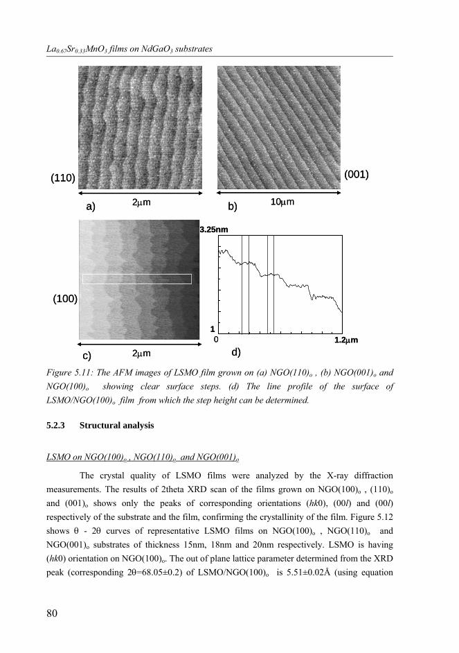
La0.67Sr0.33MnO3 films on NdGaO3 substrates
80
Figure 5.11: The AFM images of LSMO film grown on (a) NGO(110)o , (b) NGO(001)o and NGO(100)o showing clear surface steps. (d) The line profile of the surface of LSMO/NGO(100)o film from which the step height can be determined. 5.2.3 Structural analysis
LSMO on NGO(100)o , NGO(110)o and NGO(001)o
The crystal quality of LSMO films were analyzed by the X-ray diffraction measurements. The results of 2theta XRD scan of the films grown on NGO(100)o , (110)o and (001)o shows only the peaks of corresponding orientations (hk0), (00l) and (00l) respectively of the substrate and the film, confirming the crystallinity of the film. Figure 5.12 shows θ - 2θ curves of representative LSMO films on NGO(100)o , NGO(110)o and NGO(001)o substrates of thickness 15nm, 18nm and 20nm respectively. LSMO is having (hk0) orientation on NGO(100)o. The out of plane lattice parameter determined from the XRD peak (corresponding 2θ=68.05±0.2) of LSMO/NGO(100)o is 5.51±0.02Å (using equation
2µm 10µm
2µm
a) b)
c) d)
(110) (001)
(100)
3.25nm
11.2µm0
2µm 10µm
2µm
a) b)
c) d)
(110) (001)
(100)
3.25nm
11.2µm0

La0.67Sr0.33MnO3 films on NdGaO3 substrates
81
3.1) which is found to be larger than the bulk value of LSMO (The diagonal of one plane of the LSMO unit cell is 5.473Å). Also, it is larger than the out of plane lattice parameter of NGO substrate (5.428±0.013Å) determined from the substrate peak (corresponding 2θ=69.25±0.2) of the same XRD measurement.
Figure 5.12: (a), (c) and (e) shows the XRD 2θ scan of LSMO/NGO(100)o , LSMO/NGO(110)o and LSMO/NGO(001)o respectively. (b), (d) and (f) are the corresponding 2-theta scan zoomed into fourth order peak of the above samples respectively. The thicknesses of the films are 14nm, 18nm and 20nm for (a), (c) and (e) respectively.
66 68 70 721
10
100
1000
NGO (400)
LSMO (440)
Inte
nsity
2θ20 40 60 80 100 120 140
0.1
1
10
100
1000
10000
100000
1000000
1E7
(600)
(200)(400)
Inte
nsity
2θ
20 40 60 80 100 1200.1
1
10
100
1000
10000
100000
1000000
1E7
(110)(440)
(220)
(330)
Inte
nsity
2θ
LSMO/NGO(100)
LSMO/NGO(110)102 103 104 105 106 107 108 109 1101
10
100
1000
NGO (440)
LSMO (004)
Inte
nsity
2θ
0 20 40 60 80 100 1200.1
1
10
100
1000
10000
100000
1000000
(004)(003)
(002)(001)
Inte
nsity
2θ
e) f)
LSMO/NGO(001)
c) d)
a) b)
LSMO (004)
66 68 70 721
10
100
1000
NGO (400)
LSMO (440)
Inte
nsity
2θ20 40 60 80 100 120 140
0.1
1
10
100
1000
10000
100000
1000000
1E7
(600)
(200)(400)
Inte
nsity
2θ
20 40 60 80 100 1200.1
1
10
100
1000
10000
100000
1000000
1E7
(110)(440)
(220)
(330)
Inte
nsity
2θ
LSMO/NGO(100)
LSMO/NGO(110)102 103 104 105 106 107 108 109 1101
10
100
1000
NGO (440)
LSMO (004)
Inte
nsity
2θ
0 20 40 60 80 100 1200.1
1
10
100
1000
10000
100000
1000000
(004)(003)
(002)(001)
Inte
nsity
2θ
e) f)
LSMO/NGO(001)
c) d)
a) b)
LSMO (004)
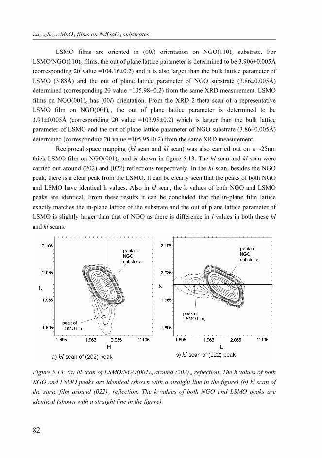
La0.67Sr0.33MnO3 films on NdGaO3 substrates
82
LSMO films are oriented in (00l) orientation on NGO(110)o substrate. For LSMO/NGO(110)o films, the out of plane lattice parameter is determined to be 3.906±0.005Å (corresponding 2θ value =104.16±0.2) and it is also larger than the bulk lattice parameter of LSMO (3.88Å) and the out of plane lattice parameter of NGO substrate (3.86±0.005Å) determined (corresponding 2θ value =105.98±0.2) from the same XRD measurement. LSMO films on NGO(001)o has (00l) orientation. From the XRD 2-theta scan of a representative LSMO film on NGO(001)o, the out of plane lattice parameter is determined to be 3.91±0.005Å (corresponding 2θ value =103.98±0.2) which is larger than the bulk lattice parameter of LSMO and the out of plane lattice parameter of NGO substrate (3.86±0.005Å) determined (corresponding 2θ value =105.95±0.2) from the same XRD measurement.
Reciprocal space mapping (hl scan and kl scan) was also carried out on a ~25nm thick LSMO film on NGO(001)o and is shown in figure 5.13. The hl scan and kl scan were carried out around (202) and (022) reflections respectively. In the hl scan, besides the NGO peak, there is a clear peak from the LSMO. It can be clearly seen that the peaks of both NGO and LSMO have identical h values. Also in kl scan, the k values of both NGO and LSMO peaks are identical. From these results it can be concluded that the in-plane film lattice exactly matches the in-plane lattice of the substrate and the out of plane lattice parameter of LSMO is slightly larger than that of NGO as there is difference in l values in both these hl and kl scans.
Figure 5.13: (a) hl scan of LSMO/NGO(001)o around (202) o reflection. The h values of both NGO and LSMO peaks are identical (shown with a straight line in the figure) (b) kl scan of the same film around (022)o reflection. The k values of both NGO and LSMO peaks are identical (shown with a straight line in the figure).
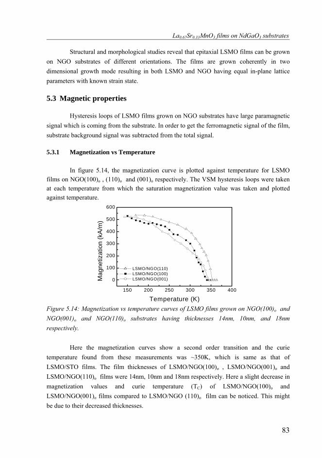
La0.67Sr0.33MnO3 films on NdGaO3 substrates
83
Structural and morphological studies reveal that epitaxial LSMO films can be grown on NGO substrates of different orientations. The films are grown coherently in two dimensional growth mode resulting in both LSMO and NGO having equal in-plane lattice parameters with known strain state. 5.3 Magnetic properties Hysteresis loops of LSMO films grown on NGO substrates have large paramagnetic signal which is coming from the substrate. In order to get the ferromagnetic signal of the film, substrate background signal was subtracted from the total signal. 5.3.1 Magnetization vs Temperature
In figure 5.14, the magnetization curve is plotted against temperature for LSMO films on NGO(100)o , (110)o and (001)o respectively. The VSM hysteresis loops were taken at each temperature from which the saturation magnetization value was taken and plotted against temperature.
Figure 5.14: Magnetization vs temperature curves of LSMO films grown on NGO(100)o and NGO(001)o and NGO(110)o substrates having thicknesses 14nm, 10nm, and 18nm respectively. Here the magnetization curves show a second order transition and the curie temperature found from these measurements was ~350K, which is same as that of LSMO/STO films. The film thicknesses of LSMO/NGO(100)o , LSMO/NGO(001)o and LSMO/NGO(110)o films were 14nm, 10nm and 18nm respectively. Here a slight decrease in magnetization values and curie temperature (TC) of LSMO/NGO(100)o and LSMO/NGO(001)o films compared to LSMO/NGO (110)o film can be noticed. This might be due to their decreased thicknesses.
150 200 250 300 350 400
0
100
200
300
400
500
600
LSMO/NGO(110) LSMO/NGO(100) LSMO/NGO(001)M
agne
tizat
ion
(kA
/m)
Temperature (K)

La0.67Sr0.33MnO3 films on NdGaO3 substrates
84
From the initial magnetic hysteresis measurements, it is observed that all films showed in-plane magnetic anisotropy (magnetic axis with in-plane easy axis). To study this anisotropy behavior in detail, hysteresis loops were taken at different in-plane field angle similarly as measured on the samples grown on STO substrates (described in the previous chapter). 5.3.2 Magnetic anisotropy
NGO (100)o and NGO (110)o
In-plane magnetic anisotropy measurements were done using vibrating sample magnetometer (VSM) at room temperature and 150K. For each film, hysteresis loops were taken at different in-plane field directions with intervals of 5°. Figure 5.15(a) shows three hysteresis loops obtained for the 15 nm thick LSMO film on NGO (100)o at room temperature, taken along 0°, 80° and 90° with respect to one edge of the substrate which is the crystal [010] direction. Figure 5.15(b) shows three hysteresis loops obtained for the 18 nm thick LSMO film on NGO(110)o at room temperature, taken along 55°, 145° and 135° with respect to one edge of the substrate direction
Figure 5.15: (a) Hysteresis loops of a LSMO on NGO (100)o of thickness 15nm, with field applied in-plane along 0°([010]), 80° and 90°([001]) with respect to one edge of the substrate crystal direction at room temperature. Here the film surface steps lies along [010] direction (b) Hysteresis loops of a LSMO on NGO (110)o of thickness 18nm, at field angles 55°([001]), 135°and 145°([1-10]) with respect to one edge of the substrate at room temperature. Here the film surface steps lies along 90º field angle.
For the LSMO/NGO(100)o film The field directions 0° and 90° were found to be the
in-plane easy and hard directions, respectively. Hysteresis loop taken at field angle 80°, very
-3 -2 -1 0 1 2 3-0.10
-0.05
0.00
0.05
0.10
Mag
netic
mom
ent (µA
m2 )
H(kA/m)
00, [010] 800
900, [001]
-2 -1 0 1 2
-0.1
0.0
0.1
Mag
netic
mom
ent (µA
m2 )
H(kA/m)
1450, [1-10] 550, [001] 1350
a) b)-3 -2 -1 0 1 2 3
-0.10
-0.05
0.00
0.05
0.10
Mag
netic
mom
ent (µA
m2 )
H(kA/m)
00, [010] 800
900, [001]
-2 -1 0 1 2
-0.1
0.0
0.1
Mag
netic
mom
ent (µA
m2 )
H(kA/m)
1450, [1-10] 550, [001] 1350
a) b)
La0.67Sr0.33MnO3 films on NdGaO3 substrates
85
close to the hard direction is also shown in the figure which has the highest coercivity compared to all loops in all other field directions (figure 5.15(a)). For the LSMO/NGO(110)o film, the field directions 55° and 145° were found to be the in-plane easy and hard directions, respectively. It is determined from the XRD analysis (as described in section 3.3.2 in chapter 3) that the in-plane crystal directions of NGO(110)o are lying 56° ([001])and 145° ([1-10]) away from one edge of the substrate. Here also, the hysteresis loop taken at field angle 135°, very close to the hard direction, shows very high coercivity compared to all loops in all other field directions (figure 5.15(b)). This peculiar behavior of coercivity with in-plane field angle will be explained later when the magnetization reversal mechanism is presented in this chapter. AFM image of the 15 nm thick LSMO film on NGO(100)o is shown in the top panel of figure 5.16(a). From each hysteresis loops taken at different in-plane field angles, remanence values were taken and plotted against the field angle (bottom panel of figure 5.16(a)). Here θ is defined as the angle between applied field direction and the [010] NGO crystal direction. A clear difference in the remanence value can be seen. There is an oscillation with periodicity of 180° with highest remanence at θ ~0° and lowest remanence at θ ~90°. From this, we can conclude that this film has a uniaxial anisotropy with the easy direction along 0° and the hard direction along 90°. Here, the 0° and 90° are the [010] and [001] crystal directions which are the easy and hard axis, respectively. This uniaxial anisotropy with [001] direction as hard (‘c’ in figure 5.1) and [010] direction ( ‘b’ in figure 5.1) as easy axis can be due to the uniaxial in-plane compressive strain of the LSMO film or it can be step induced anisotropy as seen in LSMO films grown on STO substrates. It can be seen that both step direction and easy direction coincides here. But the investigations on other LSMO films on NGO(100)o substrates having surface step directions away from the in-plane crystal directions also showed uniaxial magnetic anisotropy with easy and hard axis lying along [010] and [001] direction respectively (Data not shown here). So we can conclude that LSMO/NGO(100)o has no step induced anisotropy. The compressive strain modifies the crystal lattice of the film, which thereby modifies the magnetio-crystalline anisotropy so that the easy and hard axes lies along the crystal directions [010] and [001] respectively.
Similarly, in figure 5.16(b), AFM image of 18nm thick LSMO film on NGO(110)o is shown in the top panel and the remanence vs field angle curve is plotted in the bottom panel. The measurement done here is exactly same as for the previous sample described in figure 5.16(a). Here it is found that remanence oscillates with periodicity of 180° showing uniaxial magnetic anisotropy. The highest remanence value found to be around 58° field angle and lowest remanence at 145° field angle. That means the easy and hard axis are lying 58°[001] and 145° [1-10] away from one edge of the sample (see the AFM image in the top panel of figure 5.16(b) to understand how the field angle(θ) measured from one edge of the

La0.67Sr0.33MnO3 films on NdGaO3 substrates
86
sample). This means that the easy and hard axes are lying along the in-plane crystal directions, [001] and [1-10] respectively. Here also it is clear that the compressive strain modifies the crystal lattice of the film, which thereby modifies the magnetic crystalline anisotropy so that the easy and hard axes lies along the in-plane crystal directions [001] and [1-10] respectively. There is no contribution from the surface steps towards the magnetic anisotropy.
Compared to LSMO films on STO substrates, the anisotropy here is very strong as we can see from the remanence oscillations which has higher amplitude and it almost reaches zero at the magnetic hard direction. So the anisotropy here is much stronger than the step-induced anisotropy found in LSMO on STO at room temperature. It is also much stronger than the biaxial crystalline anisotropy at low temperature for LSMO/STO. LSMO films of different thicknesses (up to 50nm) on NGO(100)o were made and the same magnetic anisotropy results obtained for them also.
-60 0 60 120 1800.00
0.04
0.08
0.12 Hardθ = 1450
[1-10]
Easyθ = 580
[001]
Rem
anen
ce(µ
Am
2 )
Field angle (θ)
θ=58º1µm
-30 0 30 60 90 120 150 180 2100.00
0.02
0.04
0.06
0.08
Hardθ = 900
[001]
Easy θ = 00
[010]Rem
anen
ce (µA
m2 )
Field angle (θ)
θ
1µm
a) b)
[001][001]
[001]
[010]
-60 0 60 120 1800.00
0.04
0.08
0.12 Hardθ = 1450
[1-10]
Easyθ = 580
[001]
Rem
anen
ce(µ
Am
2 )
Field angle (θ)
θ=58º1µm
-30 0 30 60 90 120 150 180 2100.00
0.02
0.04
0.06
0.08
Hardθ = 900
[001]
Easy θ = 00
[010]Rem
anen
ce (µA
m2 )
Field angle (θ)
θ
1µm
a) b)
[001][001]
[001]
[010]
Figure 5.16: (a) Remanence vs in-plane field angle of 15 nm thick LSMO/NGO(100)o film at room temperature (bottom panel). Arrows denote easy and hard directions. AFM image of the same film (top panel) where the in-plane field angle (θ) is shown. The gray scale range is from 0 to 2 nm.(b) Remanence vs in-plane field angle of 18 nm thick LSMO film grown on NGO(110)o at room temperature (bottom panel). Arrows denote easy and hard directions. AFM image of the same film (top panel) where the in-plane field angle (θ) shown. The gray scale range is from 0 to 2 nm.

La0.67Sr0.33MnO3 films on NdGaO3 substrates
87
Subsequently, these magnetic anisotropy studies were performed for both the samples (LSMO grown on NGO (100)o and NGO (110)o ) at lower temperature (150K) also. Its remanence versus field angle at 150K is plotted in figure 5.17(a) and (b) respectively. As we can see from the figure, both the films show uniaxial anisotropy same as at room temperature. The easy and hard axes lies along the crystal directions [010] and [001] respectively for LSMO/NGO(100)o (figure 5.17(a)). And for LSMO/NGO(110)o , the easy and hard axes lies along the crystal directions [001] and [1-10] respectively (figure 5.17(b)). Lowering the temperature has no effect on the anisotropy behavior of the film, though the remanence value is increased compared to the remanence at room temperature.
Figure 5.17: Remanence vs in-plane field angle of 15 nm thick LSMO film grown on NGO (100)o at 150K and (b) 17nm LSMO film grown on NGO(110)o at 150K. Arrows denote easy and hard directions.
Next, magnetic anisotropy measurements were performed on LSMO films grown on
NGO(001)o substrates also. As seen in figure 5.18(a), remanence versus field angle shows an oscillation of periodicity 180º with maximum and minimum value of remanence at 135º and 45º field angles respectively. Here the field angles are measured from one edge of the substrate. Here the easy and hard axes lie along 135º and 45º respectively with respect to one edge of the substrate. So LSMO on NGO (001)o substrate also shows uniaxial anisotropy as seen for films on NGO (100)o and (110)o .
It is determined from the XRD analysis (as described in section 3.3.2 in chapter 3) that the in-plane [100] and [010] crystal directions of NGO(001)o are lying 135° and 45° away from one edge of the substrate, respectively. This means that the easy and hard axes are lying along the in-plane crystal directions. AFM image of the same film is also shown in
-60 0 60 120
0.05
0.10
0.15
0.20
0.25Hardθ = 1450
[1-10]
Easyθ = 580
[001]Rem
anen
ce(µ
Am
2 )
Field angle (θ)
150K
-30 0 30 60 90 120 150 1800.00
0.04
0.08
0.12
0.16 Hardθ = 900
[001]
Easyθ = 00
[010] 150KRem
anen
ce (µ
Am
2 )
Field angle (θ)
a) b)
-60 0 60 120
0.05
0.10
0.15
0.20
0.25Hardθ = 1450
[1-10]
Easyθ = 580
[001]Rem
anen
ce(µ
Am
2 )
Field angle (θ)
150K
-30 0 30 60 90 120 150 1800.00
0.04
0.08
0.12
0.16 Hardθ = 900
[001]
Easyθ = 00
[010] 150KRem
anen
ce (µ
Am
2 )
Field angle (θ)
a) b)

La0.67Sr0.33MnO3 films on NdGaO3 substrates
88
figure 5.18(b) where the in-plane field angle θ is seen. Although the film surface step directions are coinciding with the easy axis here, it has been made clear with other samples having different step directions that the anisotropy axes lies along the crystal directions only. There is no correlation with step direction and anisotropy axes. Here also it is clear that the compressive strain modifies the crystal lattice of the film, which thereby modifies the magnetic crystalline anisotropy so that the easy and hard axes lies along the in-plane crystal directions [100] and [010] respectively.
Figure 5.18: Remanence vs in-plane field angle of 20 nm thick LSMO film grown on NGO (001)o at room temperature. Arrows denote easy and hard directions. (b) AFM image of the same film where the in-plane field angle (θ ) is shown. The gray scale range is from 0 to 2 nm.
5.3.3 Magnetization reversal mechanism
Magnetization reversal in magnetic thin films has been the focus of intensive research for several decades for its theoretical and practical importance[18-21]. A part of the magnetization process can be attributed to a rotation of the magnetization for many magnetic materials. This is particularly true for the magnetically “hard” directions of an anisotropic magnet. There are three terms, with different physical meanings, commonly used to describe the magnetization reversal process: the nucleation field HN, which describes the field at which a change in magnetization just starts in a saturated single-domain state; the switching field HS, which is the field at which an abrupt change in magnetization occurs; and the coercivity HC, which is the field at which the magnetization changes sign[22-25]. The nucleation field is a theoretical concept and is usually difficult to determine experimentally. When magnetic
θ=45º0 50 100 150
0.00
0.04
0.08
0.12
0.16
Rem
anen
ce (µ
Am2 )
Field angle (θ)
Easy θ = 1350
[100]
Hard θ = 450
[010]
a) b)
5µm
[010]
θ=45º0 50 100 150
0.00
0.04
0.08
0.12
0.16
Rem
anen
ce (µ
Am2 )
Field angle (θ)
Easy θ = 1350
[100]
Hard θ = 450
[010]
a) b)
5µm
[010]

La0.67Sr0.33MnO3 films on NdGaO3 substrates
89
hysteresis loop is measured by changing the applied field angle in-plane or out of plane of the film, its coercivity is in general found to vary with the applied field angle. This is called angular dependence of coercivity (ADC)[26-28]. Experimentally, the magnetization reversal mechanism is usually determined from the dependence of the coercive field as a function of angle θ between magnetic field H direction and easy axis of magnetization[29-31]. For this reason, there have been numerous investigations of ADC behaviors of various magnetic films[32, 33].
Gau and Brucker have studied the angular variation of coercivity of evaporated cobalt-based films[34]. They observed that the angular variation of the coercivity curve exhibited different shapes depending upon the orientation of the easy axis, namely, a bell-shape curve for an isotropic film, an M-shape curve for a perpendicular film and a shifted M-shape curve for an oblique evaporated film having a tilted easy axis. The angular variation of coercivity results of Huang and Judy indicated that magnetization reversal in their rf sputtered Co-Cr perpendicular media followed a curling or buckling mode[35].
In studies of magnetization reversal mechanism, we seek to understand the character of the switching of a magnetic structure from one orientation of the magnetization to another. There are various routes to reversal, depending on structure size, ranging from fast, deterministic, quasi-coherent rotation in submicron-size magnetic elements to slower, stochastic domain wall nucleation and propagation in larger thin films. In hard magnetic materials, the dominating magnetization reversal process is realized by pinning of domain walls or nucleation of reversed domains. For the single domain magnets with magnetization reversal process governed by the rotation of magnetic moments, the angular dependence of coercive field HC should correspond to the theory of coherent rotation of magnetization vector and then give rise to a (cos2/3 + sin2/3)3/2 behavior of HC(θ), according to the Stoner-Wohlfarth model[20, 25, 36]. However, for magnets controlled by domain wall pinning mechanism, coercivity HC changes should correspond to Kondorsky’s relation HC/HC[0] = 1/cos(θ); for 0º<θ<90º: this relation is modified by Suponev et al[37, 38] by considering magnetization rotation process in multidomain grains which can be written in the formula,
Where y = (Da +DN)/Dc.
Here Dc and Da (= Db) are the demagnetizing factors of an ellipsoid of revolution
(easy axis = c axis) and DN is the demagnetizing factor due to the effect of magnetic anisotropy and DN = HA/MS , where HA is the anisotropy field and MS is the saturation
( ) ( ) ( )( )
( )0
20
20
02
02
00
)2.5......(....................cossin
cos0
)1.5.......(cossin
cos0
+=
+++
=
yyH
DDDDDHH
c
Nac
Nacc
θθθ
θθθθ
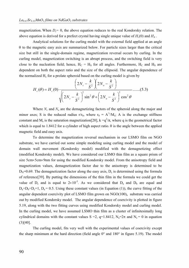
La0.67Sr0.33MnO3 films on NdGaO3 substrates
90
magnetization. When Dc= 0, the above equation reduces to the real Kondorsky relation. The above equation is derived for a prefect crystal having single unique value of Hc(0) and HA .
Analytical solutions for the curling model with the external field applied at an angle θ to the magnetic easy axis are summarized below. For particle sizes larger than the critical size but still in the single-domain regime, magnetization reversal occurs by curling. In the curling model, magnetization switching is an abrupt process, and the switching field is very close to the nucleation field; hence, HC = HS for all angles. Furthermore, HC and HS are dependent on both the aspect ratio and the size of the ellipsoid. The angular dependence of the normalized Hc for a prolate spheroid based on the curling model is given by
)3.5.......(
cos2sin2
22)0()(
22
22
2
2
22
θθ
θ
⎟⎠⎞
⎜⎝⎛ −+⎟
⎠⎞
⎜⎝⎛ −
⎟⎠⎞
⎜⎝⎛ −⎟⎠⎞
⎜⎝⎛ −
=
SkN
SkN
SkN
SkN
HH
ac
ac
cc
Where Nc and Na are the demagnetizing factors of the spheroid along the major and minor axes; S is the reduced radius r/r0, where r0 = A½/Ms; A is the exchange stiffness constant and Ms is the saturation magnetization[20], k =q2/π, where q is the geometrical factor which is equal to 1.8412 for a cylinder of high aspect ratio. θ is the angle between the applied magnetic field and easy axis.
To determine the magnetization reversal mechanism in our LSMO film on NGO substrate, we have carried out some simple modeling using curling model and the model of domain wall movement (Kondorsky model) modified with the demagnetizing effect (modified Kondorsky model). We have considered our LSMO thin film as a square prism of size 5cm×5cm×9nm for using the modified Kondorsky model. From the anisotropy field and magnetization values, demagnetization factor due to the anisotropy is determined to be DN=0.69. The demagnetization factor along the easy axis, Dc is determined using the formula of reference[39]. By putting the dimensions of the thin film in the formula we could get the value of Dc and is equal to 2×10⁻⁵. As we considered that Da and Db are equal and Da+Db+Dc=1, Da = 0.5. Using these constant values (in Equation (1)), the curve fitting of the angular dependent coercivity plot of LSMO film grown on NGO(100)o substrate was carried out by modified Kondorsky model. The angular dependence of coercivity is plotted in figure 5.19, along with the two fitting curves using modified Kondorsky model and curling model. In the curling model, we have assumed LSMO thin film as a cluster of infinitesimally long cylindrical domains with the constant values S =2, q=1.8412, Na=2π and Nc = 0 in equation (3)[40].
The curling model, fits very well with the experimental values of coercivity except the sharp minimum at the hard direction (field angle 0° and 180° in figure 5.19). The model

La0.67Sr0.33MnO3 films on NdGaO3 substrates
91
of domain wall motion which was modified by Suponev et al nicely fits in our experimental data of angular dependence of coercivity. That is, in figure 5.19, angular dependence of coercivity according to modified kondorsky model is plotted and it is seen that there is a nice fit at all field angles. Though there is a slight deviation of the experimental data near to the hard direction, it explains the sharp minimum at the hard direction.
Assuming that the film behaves purely uniaxial, one has to expect a cos(θ) dependence of the remanence signal due to the projection of the easy axis magnetization onto the axis of observation. Here we have plotted remanence also in order to show the hard and easy directions and it follows nicely the 1/cos(θ) fit as shown in figure 5.19. The plot proves unambiguously the uniaxial behavior of the films, as the measured remanence (squares) fits the 1/cos(θ) behavior (black line) nearly perfectly.
50 100 150 200 250 300
0.00
0.01
0.02
0.03
0.04
0.05
Rem
anen
ce(µ
Am
2 )
Field angle (θ)
Remanence fit (1/cosθ) Remanence (experiment)
50 100 150 200 250 300
0.0
0.5
1.0
1.5
2.0
Cio
erci
vity
(kA
/m)
Coercivity (experiment) Fit (curling model) fit (modified kondorsky)
Figure 5.19: Remanence and Coercivity vs in-plane field angle of 9nm thick LSMO/NGO(100)o , at room temperature. The solid black line is the 1/cos(θ) remanence fit. The experimental data of angular dependence of coercivity was fitted with two models namely modified Kondorsky model and curling model.
Curling model found to have good agreement with the experimental data of coercivity at all field angles except the hard direction at 90° field angle which represents the sharp minimum. But the modified Kondorsky model explains very well all the points

La0.67Sr0.33MnO3 films on NdGaO3 substrates
92
including the sharp minimas at hard directions, though there is a slight deviation near to hard direction. This slight deviation can be the experimental error. We can also explain the magnetization reversal of our LSMO film by the curling model, at all angles except at the hard direction, and at this hard direction it can be explained by the rotation of magnetization. That is, near to hard direction, the reversal mode switches from curling to uniform rotation of magnetization so that the coercivity reaches minimum or zero.
Another LSMO film of different thickness (15nm) was also measured for the angular dependence of remanence and coercivity and plotted in figure 5.20. Here also we fitted the curves using the above magnetization reversal models, and found to agree well with the experimental data.
We observed the same magnetization reversal behavior for all our LSMO films of different thicknesses, grown on different NGO substrates of all different orientations, NGO (100)o , NGO (110)o and NGO (001)o.
Figure 5.20: Remanence and Coercivity vs in-plane field angle of 15 nm thick LSMO/NGO(100)o , at room temperature. Here the LSMO film is the same as shown in figure 5.17(a) and 5.16(a). The solid back line is the 1/cos(θ) remanence fit. The experimental data of angular dependence of coercivity was fitted with two models namely modified kondorsky model and curling model.
0 30 60 90 120 150 1800.00
0.02
0.04
0.06
0.08
Remanence(Exp) 1/cos(θ) fit
Rem
anen
ce(µ
Am
2 )
Field angle (θ)
0 30 60 90 120 150 180
0
5
10
15Coercivity(exp) Modified Kondorsky Curling
Coe
rciv
ity (k
A/m
)

La0.67Sr0.33MnO3 films on NdGaO3 substrates
93
5.3.4 Magnetic force microscope (MFM) image
Magnetic force microscopy (MFM) measurements were carried out on LSMO films grown on NGO substrates of all orientations using the magnetically soft tips with CoNi layer of thickness 50nm (more details about the tips are described in section 3.4.3 of chapter 3) at room temperature.
We have grown LSMO thin films on NGO(010)o substrate also which is fairly comparable to LSMO/NGO(100)o and the only difference between them is the ‘a’ and ‘b’ lattice parameter of NGO are interchanged. Here also, the unequal in-plane compressive strain provide uniaxial magnetic anisotropy with easy axis and hard axis lying along [100] and [001] in-plane NGO crystal directions respectively which is quite similar to LSMO/NGO(100)o LSMO films.
In figure 5.21, both AFM and MFM images of LSMO films grown on NGO(010)o are shown. Here both the samples are in the remanent state after applying a magnetic field of 1500kA/m in its easy direction in the plane of the sample surface. In figure 5.21(a), AFM image of LSMO of 100nm thickness is shown and the corresponding MFM image of the same film is shown in figure 5.21(b). In the AFM image, it is visible that the film surface is rough as the thickness of the film is very high (100nm). The corresponding MFM image shows a stripe pattern with white and black contrast. This is a typical pattern seen in samples having uniaxial magnetic anisotropy.
AFM/MFM images of LSMO film on NGO(010)o having lower thickness (18nm) are also taken and it is shown in figure 5.21(c) and (d) respectively. AFM image shows clear vicinal steps on the film surface. The surface is very smooth compared to the thicker film (100nm). But the MFM image shows no magnetic contrast. This might be due to the reason that compared to thicker film, this thinner film has not enough magnetic signal to measure by an MFM tip.
MFM measurements of these films were also taken with applied magnetic field. With the maximum applied field from the set up, it was not possible to see any change in the magnetic pattern of the MFM image. That is, the field required to saturate the sample was much higher than the maximum applied field (100Oe) from the set up. LSMO films (having thicknesses even up to 100nm) grown on NGO(001)o substrate were showing hardly no magnetic contrast (not presented here) indicating that the films are having in-plane magnetic anisotropy with no out of plane component of magnetization.

La0.67Sr0.33MnO3 films on NdGaO3 substrates
94
AFM MFM
4µm 4µm
5µm 5µm
a) b)
c) d)
0
10nm
0
1º
0
2nm
0
1º
[001]
[100]
[001]
[100]
AFM MFM
4µm 4µm
AFM MFM
4µm 4µm
5µm 5µm5µm 5µm
a) b)
c) d)
0
10nm
0
1º
0
2nm
0
1º
[001]
[100]
[001]
[100]
Figure 5.21: (a) and (b) are the AFM and MFM images of LSMO film of thickness 100nm grown on NGO (010)o substrate. (c) and (d) are the AFM and MFM images of LSMO film of thickness 18nm grown on NGO (010)o substrate. The gray scale shows height in AFM image and phase in MFM image as seen in figure. 5.4 Conclusions
There is in-plane biaxial tensile strain in LSMO film grown on SrTiO3 (STO) substrate. But on the other hand, LSMO films grown on NdGaO3 (NGO) substrates experiences uniaxial compressive strain because of the larger lattice mismatch in one of the in-plane crystal direction. Due to this reason, NGO substrates were selected to grow epitaxial LSMO films in order to get different strain states than that of STO substrate. It is discovered that NGO substrates of different orientations offers different in-plane strain states and growth geometry to the LSMO film. These substrates also could get vicinal unitcell high steps on its surface by chemical and/or thermal treatment methods. Structural studies of LSMO films grown on NGO substrates of different orientations shows that the film grows epitaxial on

La0.67Sr0.33MnO3 films on NdGaO3 substrates
95
these substrates. The XRD, RHEED and AFM results of films on different NGO substrates confirms that the films grow epitaxial and in layer by layer growth mode. It is seen that LSMO/NGO(100)o film has a lattice diagonal growth giving growing planes containing either La and Sr atoms or only oxygen atoms. We have optimized the deposition conditions such that the film shows high quality structural and magnetic properties.
Magnetic anisotropy of all the films on NGO(100)o , (110)o and (001)o substrates were extensively studied and they show uniaxial anisotropy which was due to the crystalline nature of the film. Vicinal steps on the LSMO film surface have no effect on the magnetic anisotropy property of the film grown on NGO substrates of all the three orientations. For LSMO/NGO(100)o thin films, the in-plane compressive strain modifies the crystal lattice of the film, which thereby modifies the magnetic crystalline anisotropy so that the easy and hard axes lies along the in-plane substrate crystal directions [010] and [001] respectively. The film lattice gets diagonally rotated as it grows on this substrate. LSMO/NGO(110)o also has in-plane uniaxial crystalline anisotropy due to the modification of film lattice by the unequal in-plane compressive strain and the easy and hard axes lies along the in-plane substrate crystal directions [001] and [1-10] respectively. But here the film lattice grows on the substrate lattice cube on cube without any in-plane or out of plane rotation. Finally, LSMO/NGO(001)o also shows in-plane uniaxial crystalline anisotropy due to the modification of film crystal lattice by uniaxial in-plane compressive strain and the easy and hard axes lies along in-plane [100] and [010] substrate directions respectively. In here, when the film grows on the substrate, the film crystal lattice get 45º rotated in-plane with respect to the substrate lattice. Compared to LSMO films on STO substrates, the magnetic anisotropy of LSMO/NGO is much stronger, and does not change with temperature. That is, for all the films on NGO substrates of different orientations, only uniaxial crystalline anisotropy is present at all temperatures. Stripe domains are seen in MFM images of LSMO/NGO(010)o films of larger thickness indicating the strong uniaxial magnetic anisotropy of the film.
To analyze the magnetization reversal mechanism of LSMO film on NGO substrate, we have carried out some simple modeling using curling model and the model of domain wall movement (Kondorsky model) modified with the demagnetizing effect (modified Kondorsky model). The angular dependence of coercivity curves of different LSMO/NGO(100)o films were fitted with both these models and it is seen that the magnetization reversal mechanism in these LSMO films is well explained by the modified Kondorsky model.

La0.67Sr0.33MnO3 films on NdGaO3 substrates
96
5.5 References 1. S. I. Khartsev, P. Johnsson and A. M. Grishin, Colossal magnetoresistance in
ultrathin epitaxial La0.75Sr0.25MnO3 films. Journal of Applied Physics, 2000. 87: p. 2394.
2. J. Fontcuberta, J. L. Garcı´a-Mun˜oz, M. Suaaidi, B. Martı´nez, S. Pin˜ ol and X. Obradors, Competing magnetic interactions in manganese perovskites. Journal of Applied Physics, 1997. 81: p. 5481.
3. B. S. Teo, N. D. Mathur, S. P. Isaac, J. E. Evetts and M. G. Blamire, Low field magnetotransport in La0.7Sr0.3MnO3 films. Journal of Applied Physics, 1998. 83: p. 7157.
4. E. Gommert, H. Cerva, A. Rucki, R. V. Helmolt, J. Wecker, C. Kuhrt and K. Samwer, Structure and magnetoresistive properties in La–manganite thin films. Journal of Applied Physics, 1997. 81: p. 5496.
5. S. Balevicius, V. Stankeviχ, N. Zurauskiene, C. Simkevicius, J. Parseliunas, P. Cimmperman, A. Abrutis and and V. Plausinaitiene, Magneto- and Electroresistance of Ultrathin Anisotropically Strained La-Sr-MnO Films. Acta Physica Polonica A, 2005. Vol. 107(1): p. 203.
6. J.R. Sun, H.W. Yeung, H.K.Wong, T. Zhu and and B.G. Shen, Effects of vacuum annealing on the transport property of La0.67Sr0.33MnO3−δ films. European Physical Journal B, 2003. 35: p. 481-491.
7. H. K. Wong X. T. Zeng Epitaxial growth of single-crystal (La,Ca)MnO3 thin films. Applied Physics Letters, 1995. 66(24): p. 3371.
8. W. Wu, K. H. Wong and and C. L. Choy, The role of energetic plasma in pulsedlaser deposition of epitaxial manganite films. Journal of Physics. D: Applied Physics 1999. 32: p. L57-L60.
9. R. Desfeux, S. Bailleul, A. Da Costa, W. Prellier and A. M. Haghiri-Gosnet, Substrate effect on the magnetic microstructure of La 0.7Sr0.3MnO3 thin films studied by magnetic force microscopy. Applied Physics Letters, 2001. 78(23): p. 3681-3683.
10. L. A. L. Vasylechko , W. Morgenroth , U. Bismayer , A. Matkovskii and and D. Savytskii, The crystal structure of NdGaO3 at 100 K and 293 K based on synchrotron data Journal of Alloys and Compounds, 2000. 297: p. 46-52.
11. L. Malavasi, M. C. Mozzati , I. Alessandri, L. E. Depero, C. B. Azzoni and G. Flor, Sodium-Doped LaMnO3 Thin Films: Influence of Substrate and Thickness on Physical Properties. Journal of Physical Chemistry B, 2004. 108(36): p. 13643-13651.
12. D. Joonghoe, Y. N. Kim, Y. S. Hwang, J. C. Kim and N. H. Hur, Strain-induced magnetic stripe domains in La0.7Sr0.3MnO3 thin films. Applied Physics Letters, 2003. 82(9): p. 1434-1436.
13. H. Miller and A. Biswas, Temperature-dependence of magnetic domains in phase-separated manganites. Report, Univ. of Florida Physics REU 2003, 2003.
14. L. Akselrud L. Vasylechko , W. Morgenroth , U. Bismayer , A. Matkovskii , D. Savytskii, The crystal structure of NdGaO at 100 K and 293 K based on synchrotron data. Journal of Alloys and Compounds, 2000. 297: p. 46-52.
15. L.X. Cao, J. Zegenhagen, E. Sozontov and and M. Cardona, The effect of epitaxial strain on RBa2Cu3O7 thin films and the perovskite substrate. Physica C, 2000. 337: p. 24-30.

La0.67Sr0.33MnO3 films on NdGaO3 substrates
97
16. T. Ohnishi, K. Takahashi, M. Nakamura, M. Kawasaki, M. Yoshimoto and H. Koinuma, A-site layer terminated perovskite substrate: NdGaO3. Applied Physics Letters, 1999. 74(17): p. 2531-2533.
17. V. Leca, Heteroepitaxial growth of copper oxide superconductors by Pulsed Laser Deposition. Ph.D thesis, 2003, University of Twente: Enschede, The Netherlands.
18. A. Moschel, R. A. Hyman, A. Zangwill and M. D. Stiles, Magnetization Reversal in Ultrathin Films with Monolayer-Scale Surface Roughness. Physical Review Letters, 1996. 77(17): p. 3653.
19. J. M. Florczak and E. Dan Dahlberg, Magnetization reversal in (100) Fe thin films. Physical Review B, 1991. 44(17): p. 9338.
20. A. Aharoni, Introduction to the theory of ferromagnetism. 2nd ed. 2000, Newyork: Oxford University Press.
21. A. Aharoni, Angular dependence of nucleation by curling in a prolate spheroid. Journal of Applied Physics, 1997. 82(3): p. 1281-1287.
22. F. Cebollada, M. F. Rossignol, D. Givord, V. Villas-Boas and J. M. González, Angular dependence of coercivity in Nd-Fe-B sintered magnets: Proof that coherent rotation is not involved. Physical Review B, 1995. 52(18): p. 13511.
23. D. Y. Oh and J. K. Park. Crystallographic texture and angular dependence of coercivity of ordered CoPt thin film. 2005: AIP.
24. J. M. Sivertsen C. Byun, and J. H. Judy, A study on magnetization reversal mechanisms of CoCR films. IEEE Transactions on Magnetics, 1986. 22(5): p. 1155-1157.
25. S. Chikazumi and C. D. Graham, Physics of ferromagnetism. 2nd ed: Oxford : Clarendon Press, Oxford University Press.
26. D. Zhao, Liu Feng, D. L. Huber and M. G. Lagally, Step-induced magnetic-hysteresis anisotropy in ferromagnetic thin films. Journal of Applied Physics, 2002. 91(5): p. 3150-3153.
27. Y.-N Hsu S. Jeong, D. E. Laughlin, and M. E. McHenry, Magnetic Properties of Nanostructured CoPt and FePt Thin Films. IEEE Transactions on magnetics, 2000. 36(5): p. 2336-2338.
28. R. Dittrich, G. Hu, T. Schrefl, T. Thomson, D. Suess, B. D. Terris and J. Fidler, Angular dependence of the switching field in patterned magnetic elements. Journal of Applied Physics, 2005. 97: p. 10J705.
29. J.J. Wyslocki P. Pawlika, W. Kaszuwara, M. Leonowicz, Angular dependence of coercivity in Sm–Fe–N permanent magnets. Journal of Magnetism and Magnetic Materials, 2002. 242-245: p. 1344-1346.
30. P.-L. Lu and S. H. Charap, Angular Variation of Coercivity in Thin-Film Media by Micromagnetic Model. IEEE Transactions on Magnetics, 1992. 28(2): p. 986-989.
31. M. Huang and J. H. Judy, Effects of Demagnetization Fields on the Angular Dependence of Coercivity of Longitudinal Thin Film Media. IEEE Transactions on Magnetics, 1991. 27(6): p. 5049-5051.
32. R. Ranjan, J. S. Gau and and N. Amin, Comparison of angular variation of coercivity in various magnetic media. Journal of Magnetism and Magnetic Materials, 1990. 89: p. 38-46.
33. R. M. Grechishkin N.P. Suponev, M. B. Lyakhova, Y. E. Pushkar, Angular dependence of coercive field in (Sm,Zr) (Co,Cu,Fe)z alloys. Journal of Magnetism and Magnetic Materials, 1996. 157/158: p. 376-377.
34. J. S. Gau and C. F. Brucker, Angular variation of the coercivity in magnetic recording thin films. Journal of Applied Physics, 1985. 57(8): p. 3988-3990.

La0.67Sr0.33MnO3 films on NdGaO3 substrates
98
35. M. Huang and J. H. Judy, Effects of Demagnetization Fields on the Angular Dependence of Coercivity of Longitudinal Thin Film Media. IEEE Transactions on Magnetics, 1991. 27(6): p. 5049-5051.
36. D. Jiles, Introduction to magnetism and magnetic materials. 2nd ed. 1998: London [etc.] : Chapman & Hall.
37. E. Kondorsky, Journal of Physics., 1940. USSR 2 p. 161. 38. N.P. Suponev, R.M. Grechishkin, M.B. Lyakhova and Yu.E. Pushkar, Angular
dependence of coercive field in (Sm,Zr) (Co,Cu,Fe) z alloys. Journal of Magnetism and Magnetic Materials, 1996. 157/158: p. 376-377.
39. A. Aharoni, Demagnetizing factors for rectangular ferromagnetic prisms. Journal of Applied Physics, 1998. 83(6): p. 3432-3434.
40. L. Sun, Y. Hao, C.-L. Chien and P. C. Searson, Tuning the properties of magnetic nanowires. IBM Journal of Reserach and Development, 2005. 49(1): p. 79-102.

Chapter 6
Preparation and characterizations of La0.67Sr0.33MnO3 nanowires and dots
Arrays of LSMO nanodots and wires are fabricated on SrTiO3 and NdGaO3 substrates by laser interference lithography. The variation in magnetic properties with decreasing dimensions of the nanostructures is investigated in this chapter. Also, magnetic properties, especially magnetic anisotropy, Curie temperature and magnetization values of these patterned nanostructures are compared with that of thin films.
6.1 Introduction Most magnetic devices used today are based on the properties of thin-film or bulk materials. Recently it has become an attractive topic to investigate the fabrication and magnetic properties of nanoscale magnetic materials, such as nanowires [1-4], nanodots[5, 6], and nanopillars[7, 8]. Generally, to realize nanoscale dimensions two principal routes can be followed namely preparation with (1) chemical methods and (2) nanofabrication of the thin films. Nanowires, with high aspect ratio were produced by many chemical methods such as vapor-phase techniques and electrochemical template synthesis etc[9, 10]. Nanowires with lateral dimensions from 5 nm to more than 1µm and with lengths up to 100µm can be produced by electrochemical deposition[11, 12]. The major challenge with the chemical syntheses is how to place and align the resultant nanowires to the desired configurations or patterns. Nanofabrication also offers exceptional capabilities in patterning materials to very small size, and in manipulating the size, shape, orientation, and composition of the structures. In these ways making nanostructures allow us to achieve unique magnetic properties that do not exist in a thin-film or bulk material. This gives us new freedom in controlling material magnetic properties, leading to innovative magnetic materials and devices. There are different methods for making nanostructures of different dimensions and shapes by nanofabrication of

Preparation and characterizations of LSMO wires and dots
100
thin films. Optical lithography, Electron beam lithography (EBL)[13], Nanoimprint lithography[14-16] and Laser interference lithography[17] are some of these fabrication methods. Interference lithography provides a relatively inexpensive way to generate periodic structures over large areas. It has been used in a variety of applications including the fabrication of x-ray or extreme ultra-violet gratings [18], ultra-violet polarizers or filters [19], field emission arrays for flat panel displays[20] and, more recently microlens arrays for super resolution surface nanopatterning[21].
Although, there exists a large number of research works on magnetic metal nanostructures, very few studies have been carried out on patterned nanostructures of magnetic oxides. For the development of next generation spin-based devices based on La0.67Sr0.33MnO3 (LSMO), it is important to study room temperature ferromagnetism and magnetization reversal mechanism of LSMO nano-structures. Patterned La0.67Sr0.33MnO3 (LSMO) dots and wires can show different magnetic and transport characteristics compared to thin films of LSMO. Curie temperature and magnetic anisotropy are some of those properties which can be changed or modified by nano-structuring. It is interesting to study how the magnetic properties of nanowires and dots vary with its size, shape and composition.
Patterning of LSMO thin films into well characterized large area regular arrays of LSMO nanowires and dots using laser interference lithography technique is described in this chapter. The main challenges and optimization procedure of the laser interference lithography technique and ion beam etching process are discussed in section 6.2. In section 6.3, magnetic anisotropy of LSMO nanowires on STO substrates are analyzed by both vibrating sample magnetometer and torque magnetometer measurements. Also in this section, Magnetic domain imaging of LSMO dots and wires on STO substrate carried out by magnetic force microscopy is discussed. In section 6.4, both fabrication process and magnetic studies of LSMO nanowires on NGO substrates are described.
6.2 Optimization of Laser Interference Lithography and Ion Beam Etching parameters
Epitaxial LSMO films are spin coated with diluted photo resist (Arch 907 aka Olin) and patterned by exposing in Laser Interference Lithography (LIL). Then the sample is etched by Argon ion milling and ultrasonic cleaning is done in acetone to remove the photo-resist in order to get the desired patterned LSMO wires or dots. More details about LIL procedure can be found in section 3.5 of chapter 3. Different exposure time is used to get photo resist patterns, and they were found to give different pattern sizes as shown in figure 6.1. We used here 3 exposure times of 14 seconds, 28 seconds and 42 seconds respectively. For this set of samples shown in figure 6.1 we used laser energy of 172µW/cm2. It is seen that as the

Preparation and characterizations of LSMO wires and dots
101
exposure time increases from 14s to 28s and to 42s, the pattern size (here the dot diameter) decreases from 390nm to 304nm and to 210nm respectively and after a threshold value of exposure time (~1minute) the nanopattern disappears. So, for this case it is considered that the optimum exposure time is in between 14 s and 1minute. Then the optimization of etching procedure which is carried out by argon ion milling is also done. We used the acceleration voltage of 100V to accelerate the argon ions in the direction of the sample. The beam has an incident angle of 20º with the surface normal of the sample. The sample is rotated during the etching process. Beam current was 20mA and beam voltage was 500V. The etching rate of LSMO sample was found to be around 1.4nm/minute. To make sure that all the LSMO is removed, the etching time is increased so that it etches slightly into the substrate also. It is found that even after cleaning the sample with acetone for 1 hour in ultrasonic bath, the photo-resist still remains on top of the patterned structures. In figure 6.2(a) and (b), it can be seen that there remains the photo resist on top of the dots and wires. After the etching process, photo-resist becomes hardened on top of the patterned structures, and it becomes difficult to remove by ultrasonic cleaning. So some mechanical cleaning step was introduced for removing the hardened photo-resist. With cotton tips we cleaned the top surface of the sample placed in acetone bath for 1 minute. Then again ultrasonic cleaning was done in acetone for 10 minutes to clean up the residues.
Fig 6.1: Developed photoresist patterns on LSMO films grown on STO substrates, with different laser exposure time of 14 seconds, 28 seconds and 42 seconds respectively. It is clear that the dot diameter decreases with LIL exposure time.
1µm
400nm 400nm
14s 28s
42s
1µm
400nm 400nm
14s 28s
42s

Preparation and characterizations of LSMO wires and dots
102
Figure 6.2: (a) Patterned LSMO nano dots and (b) wires on STO substrates. Here the photo resist is not fully removed by the ultrasonic cleaning. In the inset of (a) it is seen that photo resist is fully removed from three dots and not removed from one dot. In (b) we see that resist remains on all wires except one which is the 6th wire from left.
Figure 6.3: Both 3-dimensional and 2 dimensional AFM images of patterned LSMO nano dots(a)&(c) and nanowires(b)&(d) respectively on STO substrates after the mechanical cleaning followed by the ultrasonic cleaning. Blow up of some part of the nanowires are also shown here where the wire edges are not sharp and straight.
In figure 6.3, the AFM images (both 3dimensional and 2dimensional) of the nano
dots and nano wires of LSMO after the cleaning step which included the mechanical cleaning,
5µma) b)5µma) b)5µm5µma) b)
90nm
2µm 5µm
40nm
a) b)
5µm 5µm
c)d)
90nm
2µm 5µm
40nm
a) b)
5µm 5µm
c)d)

Preparation and characterizations of LSMO wires and dots
103
is shown. From the images it can be clearly concluded that the hardened photo-resist can be removed completely by mechanical cleaning step. Both dots and wires show clean top surface.
6.3 Patterned La0.67Sr0.33MnO3 nano structures on SrTiO3 substrate
After optimizing the LIL exposure time, the etching time, and solving the problem of photoresist hardening on top of the nanostrucures, we achieved clean LSMO nanowires and dots of different dimensions. The AFM images of these LSMO nanowires and dots with decreasing dimensions are shown in figure 6.4 and 6.5 respectively.
Figure 6.4: AFM images (all with size 5X5µm) of patterned LSMO nanowires of different dimensions on STO substrates. Width of the wires of is written below each image. Nanowires of width down to 125nm and nanodots of diameter down to 80nm were fabricated. The periodicities of these nanostructures were either 400nm or 600nm. The periodicities of the wires in all the images in figure 6.4 were 600nm except the one with width 234nm (there the periodicity is 400nm). LSMO nanodots shown in figure 6.5 have periodicity 600nm for the first 3 samples with dot diameters of 300nm, 215nm and 152nm and the last sample with diameter of 80nm is having periodicity of 400nm. Although, dots of
322nm 283nm
234nm 125nm
5µm
322nm 283nm
234nm 125nm
5µm

Preparation and characterizations of LSMO wires and dots
104
diameter 80nm were created, the cross section of the structure looked conical in shape instead of rectangular shape.
Figure 6.5: AFM images (all with size 2X2µm) of patterned LSMO nanodots of different diameters on STO substrates. Diameter of the dots is written below each image. 6.3.1 Magnetic anisotropy
On reducing the structure sizes to dimensions comparable to relevant magnetic length scales, such as the domain-wall width or the exchange length, there arises the importance of the existence of a true single-domain state, the magnetic switching characteristics as well as the stability of the domain state[22]. Compared to thin films of LSMO, nanowires made from it may have different property of magnetic anisotropy by the effects of strain and shape. Wu et al[23] had found that sub-micron sized LSMO islands of different aspect ratio on LaAlO3 substrate has characteristic multi-domain structure with perpendicular orientation[10]. Optical lithography and ion milling were used there to pattern LSMO films to islands of diameters greater than 500nm and they were imaged by magnetic force microscopy (MFM). The domain structure in these structures was dominated by the compressive strain effects from the underlying substrate resulting in perpendicular domains. Recently magnetic oxide nano structures embedded in a paramagnetic matrix by electron beam lithography and ion implantation has been also reported[24].
152nm
300nm
2µm
215nm
80nm152nm
300nm
2µm
215nm
80nm

Preparation and characterizations of LSMO wires and dots
105
The main magnetic measurements performed on our LSMO nanowires and nanodots are magnetic anisotropy measurements done by the vibrating sample magnetometer (VSM), torque magnetometry (TM), and the magnetization switching studies carried out by magnetic force microscopy (MFM). Vibrating sample magnetometer measurements of Nanowires
As shown in the previous section, LSMO nanowires of different nano dimensions were fabricated on STO substrates. Using the VSM, we analyzed and compared the magnetic anisotropy properties of these nanowires at room temperature and 160K, and it is described in later paragraphs. First we discuss the magnetic anisotropy behavior at room temperature.
In figure 6.6, both in-plane and out of plane hysteresis loops are plotted for one of the representative LSMO nanowire sample with wire width 420nm, height 26nm and periodicity 600nm at room temperature. In this sample, the wire direction is along the [100] crystal direction and 45º away from the step direction of the film from which these patterned wires were made. In-plane hysteresis loops were taken with magnetic field applied both parallel and perpendicular to the wire direction. The coercivity found from the in-plane hysteresis loops are in the range of 1kA/m which is very small and comparable to the coercivity of LSMO/STO film. According to the in-plane and out of plane hysteresis loops in figure 6.6, it can be concluded that these nanowires have magnetic hard axis directed out of plane. In the out of plane loop it is seen that there is a small straight portion close to zero field (shown by the arrows in figure) which indicate that the wires have a small magnetic moment in the out of plane direction also.
Figure 6.6: Both in-plane (parallel to and perpendicular to wire direction) and out of plane VSM hysteresis loops of patterned LSMO nanowires of LSMO (wire width 420nm periodicity 600nm and height of 26nm) on STO substrates.
-1000 -500 0 500 1000
-0.10
-0.05
0.00
0.05
0.10 300K
Mag
netic
mom
ent(µ
Am
2 )
H(kA/m)
In-plane, // to wire In-plane, ⊥ to wire Out of plane
-1000 -500 0 500 1000
-0.10
-0.05
0.00
0.05
0.10 300K
Mag
netic
mom
ent(µ
Am
2 )
H(kA/m)
In-plane, // to wire In-plane, ⊥ to wire Out of plane
Preparation and characterizations of LSMO wires and dots
106
To analyze the in-plane magnetic anisotropy, hysteresis loops were taken at different in-plane field directions with intervals of 5° for each sample. Figure 6.7 shows hysteresis loops of three different samples of LSMO nanowires of different dimensions. These three samples are nanowires of wire width of 283nm, 146nm and 125nm with periodicity 600nm respectively. The heights (thickness) of the wires are 26nm, 43nm and 95nm respectively. Here in each graph, only the in-plane easy and hard loops were shown which are 0º and 90º respectively with respect to the wire axis. That is, the easy axis lies along the wire direction and the hard axis lies along perpendicular to the wire direction. Here, it should be noted that the wire direction is along the [100] crystal direction and 45º away from the film step direction for samples with wire widths 146nm and 125nm. But the sample with wire width 283nm, has both wire direction and film step direction along [100] crystal direction. All the three samples of nanowires showed the same result with easy axis lying along the wire direction irrespective of the wire width, periodicity, thickness, and wire direction, although the shape of the hysteresis loops are different.
Considering the shapes of the hysteresis loops of sample with wire width 283nm, it can be seen that the magnetic switching behavior along the hard and easy directions are having significant difference. In the hysteresis loop along the easy axis, the magnetic moment decreases rapidly just after the field crosses the zero value (shown in figure as part (1)) and then the change in magnetic moment is much slower with the increase in field (shown in figure as part (2)). At first a sharp switching occurs and then rather slow switching as the field increases. That is, the in-plane easy axis hysteresis loop has two distinct steps and magnetization reversal occurs in two steps. In the beginning, it seems like sharp switching is due to the domain wall motion and towards the higher field, the switching behavior changes to rotation of the moments. For the hysteresis loop along the hard direction, there is no such kind of loop shape and switching behavior. But when the dimension of the wires decreases, the hysteresis loops along the hard axis also shows the double switching behavior by sharp switching in the beginning and then the rotation of the moments.
The coercivity and remanence of the hard loop is found to be smaller than that of easy loop which is expected for a normal ferromagnetic nanowire sample. It can be also observed that the coercivity of the nanowires increases with decrease in the wire width. Reports about this enhancement of coercivity with reduction of structure size is found in many other magnetic nanostructures also which is explained by the finite size effects[25-27]. The increase in saturation magnetic moment can be attributed to the increase in thickness (height) of the wires.

Preparation and characterizations of LSMO wires and dots
107
-10 -8 -6 -4 -2 0 2 4 6 8 10-0.10
-0.05
0.00
0.05
0.10
part(2)
part(1)
300K
wire width = 283nm
easy,[100], // to wire hard, [010], ⊥ to wire
Mag
netic
mom
ent (
µAm
2 )
H(kA/m)
-10 -8 -6 -4 -2 0 2 4 6 8 10-0.10
-0.05
0.00
0.05
0.10 300K
wire width = 146nmMag
netic
mom
ent (µA
m2 )
H(kA/m)
easy,[100], // to wire hard,[010], ⊥ to wire
-10 -5 0 5 10-0.3
-0.2
-0.1
0.0
0.1
0.2
0.3 300K
wire width = 125nm
Mag
netic
mom
ent (
µAm
2 )
H(kA/m)
easy, [100], // to wire hard, [010], ⊥ to wire
Figure 6.7: VSM hysteresis loops, along in-plane easy (filled square) and in-plane hard (open circle) directions of patterned LSMO nanowires of different wire widths (283nm, 146nm and 125nm) with heights 26nm, 43nm and 95nm respectively. In-plane easy and hard axes which are 0º and 90º away from the nanowire orientation respectively.

Preparation and characterizations of LSMO wires and dots
108
There are two possible interpretations for the double switching behavior in the hysteresis loops of nanowires. They are: (1) Because of the dry etching by argon ion milling, some structural change of LSMO at the edges of the wires might have occurred which resulted in that part of the wire behave magnetically different and the side edge part and the middle part of the wires could be magnetically decoupled and thus explain the two steps hysteresis loop. There could be large structural strains at the side edges of the wires, or there can be some damages occurred at the edges of the wires due to the argon ion milling (See the zoomed in image of nanowires in figure 6.3). (2) Here the fabricated nano wires are lying along the crystal axis (100) which is crystalline hard axis according to the magneto-crystalline anisotropy of the film. That is, the magneto-crystalline easy axis ([110] direction] lies 45º away from the wire direction. So in these wires, there is a competition of two anisotropies namely biaxial magneto-crystalline anisotropy and uniaxial magneto-static (shape) anisotropy. This also can explain the double step magnetic switching. In order to investigate the origin of the double switching behavior, we have fabricated LSMO nanowires in such a way that the wire axis lies along [110] crystal direction (~45º away from one edge of the substrate). In figure 6.8(a), hysteresis loops along easy (~50º away from one edge) and hard (~135º away from one edge) directions of this particular sample are shown. Here the easy axis is along the wire direction which is the crystal direction [110]. It can be clearly seen that there is no double switching behavior in these both hysteresis loops along easy and hard directions.
Figure 6.8: (a) Hysteresis loops along easy and hard directions of nanowires (wire width=300nm, height= 20nm and periodicity= 600nm) having wire direction along [110] crystal direction of STO. (b) Hysteresis loops along the same field angles for another nanowire sample (wire width=420nm, height= 25nm and periodicity= 600nm) having wire direction along [100] direction.
To compare it with nanowires aligned along [100] direction (one edge of the substrate), we have plotted the hysteresis loops at same field angles of a previous nanowire
-8 -4 0 4 8-0.10
-0.05
0.00
0.05
0.10
300K
Mag
netic
mom
ent(µ
Am
2 )
H(kA/m)
500,[110] 1350,[1-10]
-8 -4 0 4 8-0.10
-0.05
0.00
0.05
0.10
300KMag
netic
mom
ent (µA
m2 )
H(kA/m)
Easy, 500, [110], // to wire Hard, 1350, [1-10], ⊥ to wire
a) b)
-8 -4 0 4 8-0.10
-0.05
0.00
0.05
0.10
300K
Mag
netic
mom
ent(µ
Am
2 )
H(kA/m)
500,[110] 1350,[1-10]
-8 -4 0 4 8-0.10
-0.05
0.00
0.05
0.10
300KMag
netic
mom
ent (µA
m2 )
H(kA/m)
Easy, 500, [110], // to wire Hard, 1350, [1-10], ⊥ to wire
-8 -4 0 4 8-0.10
-0.05
0.00
0.05
0.10
300K
Mag
netic
mom
ent(µ
Am
2 )
H(kA/m)
500,[110] 1350,[1-10]
-8 -4 0 4 8-0.10
-0.05
0.00
0.05
0.10
300KMag
netic
mom
ent (µA
m2 )
H(kA/m)
Easy, 500, [110], // to wire Hard, 1350, [1-10], ⊥ to wire
a) b)

Preparation and characterizations of LSMO wires and dots
109
sample which has wire direction along [100] direction (figure 6.8(b)), where the double switching can be clearly seen. In-plane hysteresis loops at different field angles were taken for both the above samples to confirm that no double switching is present in wires aligned along [110] crystal direction (figure 6.9) and double switching is present in wires aligned along [100] crystal direction (figure 6.10).
Figure 6.9: In-plane hysteresis loops of the same nanowire sample shown in figure 6.8(a) at different field angles. It is seen that the loops at all field angles have no double switching. Here all the loops have same scale as that of 180º field angle.
Figure 6.10: In-plane hysteresis loops of the same nanowire sample shown in figure 6.8(b) at different field angles. It is seen that the loops at all field angles except 180º (hard direction) and 5º shows double switching. Here all the loops have same scale as that of 180º field angle.
450
Easy ( 900)[100]// to wire
-8 -4 0 4 8-0.10
-0.05
0.00
0.05
0.10
Mag
netic
mom
ent (µA
m2 )
H(kA/m)
Hard (1800)[010]⊥ to wire
250
50
1150
450
Easy ( 900)[100]// to wire
-8 -4 0 4 8-0.10
-0.05
0.00
0.05
0.10
Mag
netic
mom
ent (µA
m2 )
H(kA/m)
Hard (1800)[010]⊥ to wire
250
50
1150
-8 -4 0 4 8-0.08
-0.04
0.00
0.04
0.08
1800M
agne
tic m
omen
t(µA
m2 )
H(kA/m)
900
Hard, (1350)[-110]⊥ to wire
Easy, (500)[110]// to wire
-8 -4 0 4 8-0.08
-0.04
0.00
0.04
0.08
1800M
agne
tic m
omen
t(µA
m2 )
H(kA/m)
900
Hard, (1350)[-110]⊥ to wire
Easy, (500)[110]// to wire

Preparation and characterizations of LSMO wires and dots
110
So, from these results, it can be concluded that the competition between the magneto crystalline anisotropy and shape anisotropy of the wires is the origin of double switching in the hysteresis loops of nanowires aligned along crystal hard direction.
In order to get a more detailed picture of the in-plane magnetic anisotropy of the wires, hysteresis loops at different in-plane field angles with 5º step were taken and then the remanence and coercivity found from these hysteresis loops were plotted against the in-plane field angle. Figure 6.11 shows the plots of remanence and coercivity against in-plane field angle of nanowire sample of width 283nm and periodicity 600nm and thickness of 46nm both at 300K and 160K. Here in this sample, the wire direction is along the crystal [100] direction.
Figure 6.11: (a) Remanence and coercivity vs field angle of patterned LSMO nanowires on STO substrates (wire width of 283nm, periodicity of 600nm and thickness of 46nm) at 300K. Easy and hard directions are shown with arrows. (c) The same measurement curve of the same sample at temperature, 160K. The remanence dip at 90º field angle is shown by an arrow and (b) shows the three dimensional AFM image of the same sample.
-45 0 45 90 135 180 225
0.06
0.08
0.10
0.12
0.14 160K
Remanence
Rem
anen
ce(µ
Am
2 )
Field angle (θ)
-45 0 45 90 135 180 225
0
1
2
3
4
5
Coe
rciv
ity(k
A/m
)
Coercivity
-45 0 45 90 135 180 225
0.02
0.04
0.06
Rem
anen
ce(µ
Am
2 )
Field angle (θ)
Remanence
-45 0 45 90 135 180 225
0.0
0.4
0.8
1.2
1.6
Hardθ = 00
Easyθ = 900
300K
Coe
rciv
ity (k
A/m
)
Coercivity
θ
1µm
a) b)
c)
[100]
-45 0 45 90 135 180 225
0.06
0.08
0.10
0.12
0.14 160K
Remanence
Rem
anen
ce(µ
Am
2 )
Field angle (θ)
-45 0 45 90 135 180 225
0
1
2
3
4
5
Coe
rciv
ity(k
A/m
)
Coercivity
-45 0 45 90 135 180 225
0.02
0.04
0.06
Rem
anen
ce(µ
Am
2 )
Field angle (θ)
Remanence
-45 0 45 90 135 180 225
0.0
0.4
0.8
1.2
1.6
Hardθ = 00
Easyθ = 900
300K
Coe
rciv
ity (k
A/m
)
Coercivity
θ
1µm
a) b)
c)
[100]

Preparation and characterizations of LSMO wires and dots
111
At 300K, it shows an oscillation of periodicity 180º with respect to the field angle which confirms the in-plane uniaxial magnetic anisotropy (Figure 6.11(a)). Easy axis found to be lying along the wire direction and hard axis was perpendicular to the wire direction. As shown in the three dimensional AFM image in figure 6.11(b) the angle of applied magnetic field (θ) was taken with respect to one edge of the sample. The edges of the AFM image and the edges of the sample have the same direction.
At lower temperature(160K), remanence shows a difference in its oscillation behavior with extra dip in the curve at around 90º field angle (shown with an arrow in figure 6.11(c)), indicating that there is a contribution of biaxial anisotropy also. The same result is observed in different samples of nanowires having different dimensions, both at 300K and 160K. Only the result of one sample is shown here.
At room temperature, uniaxial anisotropy can be due to either the shape of the wires or uniaxial strain relaxation. This uniaxial anisotropy dominates over the magneto-crystalline anisotropy, or step induced anisotropy of the LSMO at room temperature. When the temperature is decreased, biaxial magneto-crystalline anisotropy comes into play similar to the behavior of LSMO thin films which is described in chapter 4. So, when LSMO film is patterned into nanowires, the magneto-crystalline anisotropy appears at lower temperature though the shape anisotropy is also present. To study more on the anisotropy of LSMO nanowires, magnetic torque measurements were carried out on few samples. As explained in the previous chapter, torque analysis gives a detailed and quantitative picture on the anisotropy behavior of these patterned wires. Torque measurements of nanowires
More direct and quantitative measurements of the anisotropies of these nanowires can be carried out by Torque magnetometry. As explained in chapter 4, magnetic anisotropy studies done on LSMO films on STO substrates by torque magnetometer shows combination of biaxial and uniaxial magnetic anisotropy. Torque curves were plotted at different temperatures for two different LSMO nanowires samples on STO substrates. In figure 6.12 the AFM images of these two samples are shown indicating the field angle, θ. The wire directions are at an angle θ = 0º (for the wires in 6.12(a) and (b)) with respect to an edge of the sample which is the [100] crystal direction. In figure 6.13(a), torque curves of two different nanowire samples at 20K and 200K are shown in the bottom and top panel respectively. Here also we have subtracted the background from the torque signal of the sample as explained in chapter 4. Here the oscillation of periodicity 90º corresponds to the biaxial anisotropy and the oscillation with 180º periodicity corresponds to the uniaxial anisotropy. A mixture of biaxial and uniaxial anisotropy is found here. For the above two

Preparation and characterizations of LSMO wires and dots
112
samples shown in figure 6.12(a) and (b) the field angles (θ) corresponding to the magnetic easy axes determined from the torque curves were, θ = 5±10º and (θ+90º) = 90±10º (here the sample shown in figure 6.12(b) was placed in the torque meter 90º rotated) for the uniaxial anisotropy and 45±10º for the biaxial anisotropy which corresponds to the wire direction and the crystal [110] direction respectively. That is, the uniaxial anisotropy has easy axis lying along the wire direction and biaxial anisotropy has easy axis along [110] crystal direction confirming the VSM results. The volume of the LSMO nanowire samples are calculated to be equal to 210±35×10-15 m3 and 300±35×10-15 m3 for figure 6.13(a) and (b) respectively. From these torque curves, both the uniaxial and biaxial anisotropy constants were extracted using Fourier analysis and they found to be decreasing with temperature. In figure 6.13(b), both uniaxial (top panel) and biaxial (bottom panel) anisotropy constants are plotted against temperature. The decrease in both anisotropy constants is found to be independent of the dimensions of LSMO nanowires. It can be seen that as the temperature increases beyond 200K, the error bar in the anisotropy constants increases because of the background torque signal and the limit of sensitivity of the torque meter.
Figure 6.12: AFM images of LSMO nanowires (a) having width 234nm, height 26nm & periodicity 400nm and (b) width 283nm, height 46nm & periodicity 600nm. It is possible to calculate the magneto-static anisotropy energy (Ems) of one magnetic nanowire from its magnetization value using the formula[28],
)1.6.......(....................21 2
0 MNE dms µ= where Nd is the demagnetization factor of the sample. Here we consider the wire as a spheroid (rod) or rectangular prism, with semi major axis ‘c’ along the length of the wire. Here one of the semi minor axis ‘a’ is along the width of the wire and other minor axis ‘b’ is along the height of the wire. Using these dimensions of a particular nanowire, its demagnetization factors along all these directions Na, Nb and Nc can be extracted. The equation derived by Aharoni et al is used for this purpose[29].
5µm 5µm
θθ
a) b)[100] [100]
5µm 5µm
θθ
a) b)5µm 5µm
θθ
a) b)[100] [100]

Preparation and characterizations of LSMO wires and dots
113
Figure 6.13: (a) Torque curves of patterned LSMO nanowires having different dimensions (top panel and bottom panel) at 200K and 20K (b) Uniaxial magneto-static and biaxial magneto-crystalline anisotropy constants (Ku and K1) plotted against temperature shown in the top and bottom panel respectively (wire widths(w), heights(h) and periodicities(p) are shown in the legend).
As we consider only the in-plane magneto-static anisotropy of the nanowire, the demagnetization component in a direction out of plane of the nanowire sample (Nb) is not taken here. From equation 6.1, the shape anisotropy (magneto-static) constant can be derived[28], and it can be written as,
)2.6.....(..........)(21 2
0 MNNK cas −= µ Using the above equation the shape anisotropy constant can be determined if the magnetization value is known. As the experimental value of magnetization from the VSM measurement for an array of nanowires sample (width = 420nm, height = 26nm and periodicity = 600nm) in an area 5×5 mm is known (magnetization curve of a similar sample can be found in figure 6.15) at different temperature, Ks can be determined and it is plotted against temperature (here the volume of the nanowires = 252±35×10-15 m3). Although in this case there are many nanowires, we are considering the Na (=0.08)and Nc (=6.6 × 10⁻⁶) values
0 50 100 150 200 250 300 350 4000
5
10
-K1 (
103 J/
m3)
Temperature (K)
w = 234nm, p = 400nm, h = 26nm w = 283nm, p = 600nm, h = 46nm
0
2
4
6
8
10
Ku (1
03 J/m
3 )
w = 234nm, p = 400nm, h = 26nm w = 283nm, p = 600nm, h = 46nm
a) b)0 100 200 300 400
-0.03
0.00
0.03w = 283nm, p = 600nm, h = 46nm
20K 200K
-Tor
que
(10 -7
Nm
)
Field angle (θ+900)
-0.02
0.00
0.02w = 234nm, p = 400nm, h = 26nm
Torq
ue (1
0 -7N
m)
200K 20K
0 100 200 300 400 Field angle (θ)

Preparation and characterizations of LSMO wires and dots
114
for only one nanowire. In figure 6.14, Ks is plotted against temperature where the uniaxial anisotropy constant (Ku) determined from the torque measurement is also plotted for comparison. It can be seen that Ku and Ks are of the same order, but there is a factor of two difference. This can be due to the reason that we considered only one nanowire for the calculation and there is an array of wires where the wires can have mutual interaction which can reduce their total anisotropy.
Figure 6.14: Uniaxial anisotropy constant (Ku) from torque measurement and calculated shape anisotropy constant (Ks) which are plotted against temperature for a nanowire sample of width =420nm, height =26nm and periodicity = 600nm. 6.3.2 Magnetization vs Temperature
In order to study the influence of nano patterning in the magnetic properties especially curie temperature of LSMO, magnetic hysteresis loops of both nanowires and dots were taken at different temperature. From these loops saturation magnetic moments are extracted for each temperature. Also, by knowing the height, periodicity, width/diameter of the wires/dots and area of the sample surface, it is possible to calculate the volume and thus the magnetization of the LSMO nanowires and dots. In figure 6.15, the magnetizations versus temperature curves are shown for both nanowires and dots of width 283nm and diameter 180nm respectively. The heights of both wires and dots are 46nm and 44nm respectively and their periodicity is 600nm. Here the volume of the LSMO nanowires is calculated to be equal to (229±35)×10-15 m3 and of the nanodots is equal to (126±20)×10-15 m3. Even though there is a notable error bar (There can be error in determining the exact width and diameters of the nanostructures using AFM. Also there can be some small parts of the sample where the nanostructures are removed) in the calculated volume of the magnetic nanostructures, the magnetization values are comparable with that of LSMO films at different temperatures. The
0 100 200 300 400
0
5
10
15
Na=0.08 N
c=6.6 x10⁻⁶
Ani
sotro
py c
onst
ant (
103 J/
m3 )
Temperature(K)
Ks Ku
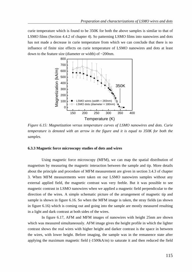
Preparation and characterizations of LSMO wires and dots
115
curie temperature which is found to be 350K for both the above samples is similar to that of LSMO films (Section 4.4.2 of chapter 4). So patterning LSMO films into nanowires and dots has not made a decrease in curie temperature from which we can conclude that there is no influence of finite size effects on curie temperature of LSMO nanowires and dots at least down to the feature size (diameter or width) of ~200nm.
Figure 6.15: Magnetization versus temperature curves of LSMO nanowires and dots. Curie temperature is denoted with an arrow in the figure and it is equal to 350K for both the samples. 6.3.3 Magnetic force microscopy studies of dots and wires
Using magnetic force microscopy (MFM), we can map the spatial distribution of
magnetism by measuring the magnetic interaction between the sample and tip. More details about the principle and procedure of MFM measurement are given in section 3.4.3 of chapter 3. When MFM measurements were taken on our LSMO nanowires samples without any external applied field, the magnetic contrast was very feeble. But it was possible to see magnetic contrast in LSMO nanowires when we applied a magnetic field perpendicular to the direction of the wires. A simple schematic picture of the arrangement of magnetic tip and sample is shown in figure 6.16. So when the MFM image is taken, the stray fields (as shown in figure 6.16) which is coming out and going into the sample are mostly measured resulting in a light and dark contrast at both sides of the wires.
In figure 6.17, AFM and MFM images of nanowires with height 25nm are shown which was measured simultaneously. AFM image gives the height profile in which the lighter contrast shows the real wires with higher height and darker contrast is the space in between the wires, with lower height. Before imaging, the sample was in the remanence state after applying the maximum magnetic field (-1500kA/m) to saturate it and then reduced the field
150 200 250 300 350 400
0
100
200
300
400
500
600
700
800
350K
LSMO wires (width = 283nm) LSMO dots (diameter = 180nm)M
agne
tizat
ion
(kA
/m)
Temperature (K)

Preparation and characterizations of LSMO wires and dots
116
to zero, in the in-plane direction perpendicular to the LSMO wire axis. The MFM imaging was done with in-plane magnetic field applied in a direction perpendicular to the wires. We have applied magnetic field in the order +100 Oe, 0 and -100 Oe respectively. There is three parts in the MFM image shown in figure 6.17(b), and they are, the top part where the magnetic field of 100 Oe is applied to the right (H = +100Oe), then the middle part where the magnetic field decreased to zero and finally the bottom part where the magnetic field of 100Oe is reversed towards left direction (H = -100Oe).
Figure 6.16: Schematic picture of the magnetic tip and cross section of the LSMO nanowire where the field lines are shown.
Magnetic field of 100 Oe (~ 8kA/m) was the maximum field which we could apply
in our set up and it was enough to saturate the LSMO nanowires in its hard direction, which is perpendicular to the wire direction. When this field is applied, the wires are in single domain state where all the spins lie in the direction of the applied field. Then we reduced the magnetic field to zero and the magnetic contrast becomes very feeble showing that the wires now returned to its remanence state. In this state also light and dark contrast still remains but it is not as strong as the saturated state (middle part of the MFM image in figure 6.17(b)). Here in the remanent state the magnetization orientation still remains in the previously applied field direction (from left to right in the figure), and the contrast is feeble because of the magnetization is reduced from its saturation value. When we reverse the field of 100 Oe in opposite direction, the wires get saturated in the opposite direction and all the spins align in the direction of the field. In this case, the light and dark contrast of the MFM image interchanges (bottom part of the MFM image in figure 6.17(b)). Because of the thermal drifting of the sample during scanning of the image, the wires look bended and not seemed to be straight.
Ni (50nm)
STO
LSMO
Tip
Strayfieldlines
Ni (50nm)
STO
LSMO
Tip
Strayfieldlines

Preparation and characterizations of LSMO wires and dots
117
Fig 6.17: Left figure shows the AFM image of patterned LSMO nanowires where the lighter contrast shows the real wires with higher height and darker contrast is the space in between the wires, with lower height. The corresponding MFM image of the wires is shown in the right figure which is divided into top, middle and bottom parts. As shown in figure, the magnetic field applied is varied in these three parts, as 100 Oe towards right direction in top part, 0 field in middle part and 100 Oe applied towards left direction in the bottom part respectively.
Figure 6.18: (a) MFM image of the patterned LSMO nanodots (diameter ~ 250nm, height = 35nm and periodicity = 600nm) on STO substrate. (b) MFM image taken only on one of the dots where the domain wall switching is shown by an arrow.
3µm 3µm
H = +100Oe
H = -100Oe
H = 0 Oe
AFM MFM
a) b)3µm 3µm
H = +100Oe
H = -100Oe
H = 0 Oe
AFM MFM
a) b)
1µm 500nm
Applied field direction
Domain wall switchinga) b)1µm 500nm1µm 500nm
Applied field direction
Domain wall switchinga) b)

Preparation and characterizations of LSMO wires and dots
118
In figure 6.18(a), MFM images of LSMO nanodots (diameter = 250nm, height = 35nm) on STO substrate are shown. Here also the sample was in the remanence state after applying the maximum magnetic field (+1500kA/m) to saturate it in the in-plane direction of the LSMO dots We can see the magnetic contrast on each dot where the outer parts of the dots are having more dark contrast. This means that the tip is being more attracted at the edges of the dots. The magnetic flux closure occurs at the outer edges of the dots resulting stronger out of plane component of magnetization of the sample at the edges. Domain walls also are visible inside the dots and when we closely look into one of the dot (figure 6.18(b)) the domain wall switching can be clearly seen (shown with an arrow). It might be due to the reason that the sample is magnetically softer than the tip so that the tip can switch the domains in LSMO nanodots.
6.4 Patterned La0.67Sr0.33MnO3 nanowires NdGaO3 substrates LSMO nanowires on NdGaO3 (NGO) substrates also were fabricated by LIL. LSMO thin films on NGO(010) and NGO(110)o substrates were patterned to nanowires by the same procedure which has been explained earlier in previous section where the nanowires on SrTiO3 substrate were made. After optimizing the LIL exposure time, the etching time, we could finally achieve clean LSMO nanowires of different dimensions on NGO substrates. Here also, the problem of photo resist hardening on top of the nanostrucures was present and the same procedure (as that of nanowires on STO) of mechanical cleaning was performed to remove the photo resist. 6.4.1 LSMO wires on NGO(110)o
LSMO nanowires were fabricated on NGO(110)o substrate by laser interference lithography. Magnetic anisotropy measurements were carried out on these samples using VSM at room temperature. The in-plane hysteresis loops along hard and easy directions of one of the representative nanowire sample (wire width = 300nm, height = 20nm and periodicity 600nm) are plotted in figure 6.19(a). AFM image of these wires also is shown (figure 6.19(b)).
In this measurement, the easy axis and hard axis are found to be lying along the crystal directions [001] and [1-10] respectively. There found to be no correlation between the wire direction and easy axis. The sample has uniaxial magnetic anisotropy which is determined by the magneto crystalline nature of LSMO and not by the shape anisotropy of the wires. Similar to the LSMO film on NGO(110)o substrate, the patterned wires also show quite strong magneto-crystalline anisotropy.

Preparation and characterizations of LSMO wires and dots
119
Figure 6.19: (a) Hysteresis loops along easy ([001]) and hard ([1-10]) directions of nanowires on NGO(110)o substrate at room temperature. Here these easy and hard in-plane crystal directions are 145º and 55º degree away from the substrate edge as shown in the AFM image (b). 6.4.2 LSMO wires on NGO(010)
The AFM images of the LSMO nanowires with decreasing dimensions (wire width of 664nm, 300nm, 175nm, and 146nm) on NGO(010)o substrates are shown in figure 6.20.
Fig 6.20: AFM images (all with size 5×5µm) of patterned LSMO nanowires of different dimensions on NGO substrates. Width of the wires is written below each image.
-10 -8 -6 -4 -2 0 2 4 6 8 10-0.10
-0.05
0.00
0.05
0.10
Easy, 1450 Hard, 550
Mag
netic
mom
ent (µA
m2 )
H(kA/m)
5µm
θ=55º
b)a)
θ=145º
[001][1-10]
-10 -8 -6 -4 -2 0 2 4 6 8 10-0.10
-0.05
0.00
0.05
0.10
Easy, 1450 Hard, 550
Mag
netic
mom
ent (µA
m2 )
H(kA/m)
5µm
θ=55º
b)a)
θ=145º
[001][1-10]
175nm 146nm
664nm 300nm
5µm
175nm 146nm
664nm 300nm
5µm
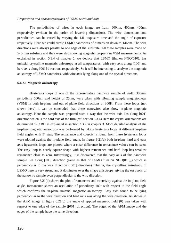
Preparation and characterizations of LSMO wires and dots
120
The periodicities of wires in each image are 1µm, 600nm, 400nm, 400nm respectively (written in the order of lowering dimension). The wire dimensions and periodicities can be varied by varying the LIL exposure time and the angle of exposure respetively. Here we could create LSMO nanowires of dimension down to 146nm. The wire directions were always parallel to one edge of the substrate. All these samples were made on 5×5 mm substrate and they were also showing magnetic property in VSM measurements. As explained in section 5.3.4 of chapter 5, we deduce that LSMO film on NGO(010)o has uniaxial crystalline magnetic anisotropy at all temperatures, with easy axis along [100] and hard axis along [001] directions respectively. So it will be interesting to analyze the magnetic anisotropy of LSMO nanowires, with wire axis lying along one of the crystal directions. 6.4.2.1 Magnetic anisotropy Hysteresis loops of one of the representative nanowire sample of width 300nm, periodicity 600nm and height of 25nm, were taken with vibrating sample magnetometer (VSM) in both in-plane and out of plane field directions at 300K. From these loops (not shown here) it can be concluded that these nanowires also show in-plane magnetic anisotropy. Here the sample was prepared such a way that the wire axis lies along [001] direction which is the hard axis of the film (ref. section 5.3.4) Here the crystal orientations are determined by XRD as explained in section 3.3.2 in chapter 3. More detailed analysis of the in-plane magnetic anisotropy was performed by taking hysteresis loops at different in-plane field angles with 5º step. The remanence and coercivity found from these hysteresis loops were plotted against the in-plane field angle. In figure 6.21(a) both in-plane hard and easy axis hysteresis loops are plotted where a clear difference in remanence values can be seen. The easy loop is nearly square shape with highest remanence and hard loop has smallest remanence close to zero. Interestingly, it is discovered that the easy axis of this nanowire sample lies along [100] direction (same as that of LSMO film on NGO(010)o) which is perpendicular to the wire direction ([001] direction). That is, the crystalline anisotropy of LSMO here is very strong and it dominates over the shape anisotropy, giving the easy axis of the nanowire sample even perpendicular to the wire direction.
Figure 6.21(b) shows the plot of remanence and coercivity against the in-plane field angle. Remanence shows an oscillation of periodicity 180º with respect to the field angle which confirms the in-plane uniaxial magnetic anisotropy. Easy axis found to be lying perpendicular to the wire direction and hard axis was along the wire direction. As shown in the AFM image in figure 6.21(c) the angle of applied magnetic field (θ) was taken with respect to one edge of the sample ([001] direction). The edges of the AFM image and the edges of the sample have the same direction.

Preparation and characterizations of LSMO wires and dots
121
Fig 6.21: (a) In-plane hysteresis loops of patterned LSMO nanowires on NGO(010)o substrate (wire width of 300nm, periodicity of 600nm and height of 25nm) at 300K with field applied along easy and hard directions. (b) Remanence and coercivity vs field angle (c) and AFM image of the same sample where field angle θ is shown.
It is clear that at room temperature, magneto-crystalline anisotropy of LSMO on
NGO(010)o dominates over the shape anisotropy of the wires. Similar to the LSMO film on NGO(010)o substrate (chapter 5), the patterned wires also show quite strong magneto-crystalline anisotropy which is comparable to the anisotropy result shown by the nanowires on NGO(110)o substrate. Also it can be noted here that these nanowires also have the same “M” shape coercivity curve as that of LSMO film. 6.4.3 Magnetic force microscopy
MFM images of LSMO nanowires (width = 665nm, height = 25nm and periodicity =
1µm) fabricated on NGO(010)o substrates were also taken using different magnetic tips. In figure 6.22, both AFM and MFM images of LSMO nanowires are shown which was
0 45 90 135 1800.00
0.02
0.04
0.06
0.08
0.10
0.12
Rem
anen
ce(µA
m2 )
Field angle (θ)
Remanence
0 45 90 135 180
0.0
0.2
0.4
0.6
Coercivity
Coe
rcivi
ty (k
A/m
)
5µm
θ
-10 -8 -6 -4 -2 0 2 4 6 8 10
-0.1
0.0
0.1 easy, 900
hard, 00
wire width = 300nmMag
netic
mom
ent (µ
Am
2 )
H (kA/m)
a)
b) c)
[100]
[001]
[100]
0 45 90 135 1800.00
0.02
0.04
0.06
0.08
0.10
0.12
Rem
anen
ce(µA
m2 )
Field angle (θ)
Remanence
0 45 90 135 180
0.0
0.2
0.4
0.6
Coercivity
Coe
rcivi
ty (k
A/m
)
5µm
θ
-10 -8 -6 -4 -2 0 2 4 6 8 10
-0.1
0.0
0.1 easy, 900
hard, 00
wire width = 300nmMag
netic
mom
ent (µ
Am
2 )
H (kA/m)
a)
b) c)
[100]
[001]0 45 90 135 180
0.00
0.02
0.04
0.06
0.08
0.10
0.12
Rem
anen
ce(µA
m2 )
Field angle (θ)
Remanence
0 45 90 135 180
0.0
0.2
0.4
0.6
Coercivity
Coe
rcivi
ty (k
A/m
)
5µm
θ
-10 -8 -6 -4 -2 0 2 4 6 8 10
-0.1
0.0
0.1 easy, 900
hard, 00
wire width = 300nmMag
netic
mom
ent (µ
Am
2 )
H (kA/m)
a)
b) c)
[100]
[001]
[100]

Preparation and characterizations of LSMO wires and dots
122
measured with a magnetic tip of CoNi layer (thickness = 35nm) as coating. This measurement was taken with out any applied magnetic field. In order to distinguish the wires from surrounding, some rectangles are drawn on top of the image as seen in figure.
Fig 6.22: Left figure shows the AFM image of patterned LSMO nanowires on NGO(010)o
substrate where the lighter contrast shows the wires with higher height and darker contrast is the space in between the wires, with lower height ( The wires are arrow marked in figure). The corresponding MFM image of the wires is shown in the right figure where the wires are denoted by rectangles. Here the tip was coated with CoNi layer of thickness 35nm.
Fig 6.23: Left figure shows the AFM image of patterned LSMO nanowires on NGO(010)o
substrate where the lighter contrast shows the wires with higher height and darker contrast is the space in between the wires, with lower height (One of the wire is arrow marked in the figure). The corresponding MFM image of the wires is shown in the right figure where the wire is denoted by a rectangle. Here the tip was coated with Ni layer of thickness 20nm.
AFM MFM
wire
5µm 5µm
wire
AFM MFM
wire
5µm 5µm
wire
AFM MFM
wires
5µm 5µm
wires
AFM MFM
wires
5µm 5µm
wires
Preparation and characterizations of LSMO wires and dots
123
In the MFM image, white contrast is seen in between the wires and inside the wires there is black contrast. This means that the tip is more attracted on the magnetic LSMO nanowires than on the spaces between the wires. But in this measurement the magnetic structure in the sample is being switched by the magnetic tip used, because the sample is magnetically much softer than the tip. This phenomenon, we can notice in the MFM image as a sharp black to white contrast appearing while the tip is scanning in the horizontal direction. So it can be concluded that with this kind of MFM tip, it is not possible to see the magnetic domain structures of the nanowire sample as the tip is largely influencing the sample.
Magnetically softer tips with a different magnetic layer coating were used to get better MFM images of the nanowires. For this, the tips coated with Nickel layer of smaller thickness (20nm) were specially prepared. In figure 6.23, both AFM and MFM images taken with this special magnetic tip is shown. Here also wires are denoted with filled rectangle and transparent rectangle both in AFM and MFM images respectively. It is seen that MFM images has darker black contrast on top of the wires and lighter contrast on between the wires. This means the tip get attracted when it scans on the wires as the wires are magnetic and the tip has no attraction in between the wires. As the magnetic contrast is very weak, we could not find any domain patterns inside the wires.
6.5 Conclusions Magnetic nanowires and dots of LSMO were fabricated from the thin films of LSMO grown on STO and NGO substrates. We have used Laser Interference Lithography technique to fabricate these nanowires and dots of different dimensions. Nanodots and wires on STO substrates were having diameter and width down to 80nm and 125nm respectively. Nanowires fabricated on NGO substrates were having width down to 146nm.
Magnetic measurements were performed on these nanowires and dots using vibrating sample magnetometry (VSM), magnetic force microscopy (MFM) and torque magnetometry (TM). The results from these measurements reveal that nanowires on STO substrate have uniaxial magneto-static anisotropy (shape anisotropy) with easy axis lying along the wire direction and hard axis perpendicular to the wire direction. As of LSMO films, biaxial magneto-crystalline anisotropy was also present in these wires which have been measured both by VSM and TM and this becomes prominent at lower temperatures. Compared to LSMO films on STO substrates which show a combination of two magnetic anisotropies, namely biaxial crystalline anisotropy and step induced uniaxial anisotropy, nanowires on STO substrate also shows combination of two anisotropies which are uniaxial shape anisotropy and biaxial crystalline anisotropy. The shape anisotropy constant calculated from the magnetization value and the demagnetization factors of a particular nanowire at

Preparation and characterizations of LSMO wires and dots
124
different temperatures is found to be comparable to (to within a factor of 2, probably because of interactions between the wires) the measured shape anisotropy constant of an array of nanowires from the torque data.
Double switching behavior is seen in hysteresis loops of LSMO nanowires with wire axis along one edge of the substrate ([100]) direction. When the wire axis is changed to [110] crystal direction of STO the double switching behavior disappears. That is, the origin of double switching behavior can be attributed to the competition between the magneto crystalline anisotropy and shape anisotropy of the nanowires. The curie temperature of LSMO nanodots and wires are found to be same as that of LSMO film, and there found no influence of finite size effects down to the dimension of 180nm. Magnetic flux closure occurs at the outer edges of the dots fabricated on STO substrate giving stronger out of plane component of magnetization of the sample at the edges. Domain walls also were visible inside the dots which are being switched by the tip because of the strong interaction between the sample and the magnetic tip. From the magnetic contrast of the wires in the MFM measurement it can be concluded that with the maximum applied in-plane magnetic field in the MFM set up, the wires can be saturated in a direction perpendicular to the wire axis.
Magnetic anisotropy measurements of LSMO nanowires on NGO(010)o and NGO(110)o substrates were performed using VSM and the results shows that the wires have uniaxial magneto crystalline anisotropy dominated over shape anisotropy at room temperature. Similar to the LSMO films on NGO(010)o and NGO(110)o substrates, the patterned LSMO nanowires on these respective substrates also show quite strong magneto-crystalline anisotropy. Here LSMO wires on NGO(110)o substrates have easy axis along [001] direction and hard axis along [1-10] directions which are 55º and 140º away from the wire directions. For LSMO wires on NGO(010)o substrates have easy axis along [100] direction which is even perpendicular to the wire direction. It is interesting to note that compared to nanowires on STO substrates, the nanowires on NGO(110)o and NGO(010)o substrates have easy axis not along the wire direction, but along 55º or even 90º (perpendicular) away from the wire direction respectively. MFM images of the wires show large influence of the tip on the sample when CoNi tip was used. Then, rather magnetically softer Ni tip was used for imaging this sample and the results shows magnetic contrast for the wires but the magnetic signal was found to be very weak.
With the results mentioned in this chapter, it can be concluded that down sizing the LSMO nanowires and dots up to the size of 100nm (width or diameter) has very little effect on its curie temperature compared to that of thin films, although the coercivity is enhanced. Also, it is clear that for the nanostructures on STO substrate, magnetic anisotropy is mostly governed by the shape of the magnetic entity, whereas the nanowires on NGO substrates have strong magneto crystalline anisotropy dominating over its shape anisotropy. In future, it will

Preparation and characterizations of LSMO wires and dots
125
be interesting to study in detail the magnetic configurations and mutual interactions of nanostructures of LSMO and their magnetoresistive response because many of the present efforts are now oriented towards lateral size reduction of continuous layers of novel magnetic materials to minimize the size of potential devices. 6.6 References 1. H. J. Elmers, J. Hauschild, H. Höche, U. Gradmann, H. Bethge, D. Heuer and U.
Köhler, Submonolayer Magnetism of Fe(110) on W(110): Finite Width Scaling of Stripes and Percolation between Islands. Physical Review Letters, 1994. 73(6): p. 898.
2. J. Shen, R. Skomski, M. Klaua, H. Jenniches, S. Sundar Manoharan and J. Kirschner, Magnetism in one dimension: Fe on Cu(111). Physical Review B, 1997. 56(5): p. 2340.
3. J. de la Figuera, M. A. Huerta-Garnica, J. E. Prieto, C. Ocal and R. Miranda, Fabrication of magnetic quantum wires by step-flow growth of cobalt on copper surfaces. Applied Physics Letters, 1995. 66(8): p. 1006-1008.
4. A. Dallmeyer P. Gambardella, K. Maiti, M. C. Malagoli, W. Eberhardt, K. Kern, C. Carbone, Ferromagnetism in one-dimensional monatomic metal chains. Nature, 2002. 416: p. 301-304.
5. M. Giovannini H. Brune, K. Bromann, and K. Kern, Self-organized growth of nanostructure arrays on strain-relief patterns. Nature, 1998. 394: p. 451-453.
6. S. I. Woods, J. R. Kirtley, Shouheng Sun and R. H. Koch, Direct Investigation of Superparamagnetism in Co Nanoparticle Films. Physical Review Letters, 2001. 87(13): p. 137205.
7. O. Fruchart, M. Klaua, J. Barthel and J. Kirschner, Self-Organized Growth of Nanosized Vertical Magnetic Co Pillars on Au(111). Physical Review Letters, 1999. 83(14): p. 2769.
8. M. Klaua O. Fruchart, J. Barthel and J. Kirschner, Growth of self-organized nanosized Co pillars in Au(111) using an alternating deposition process. Applied Surface Science, 2000. 162-163: p. 529-536.
9. Bridget Wildt, Prashant Mali and Peter C. Searson, Electrochemical Template Synthesis of Multisegment Nanowires: Fabrication and Protein Functionalization. Langmuir, 2006. 22: p. 10528-10534.
10. X. T. Zhang, Z. Liu, K. M. Ip, Y. P. Leung, Li Quan and S. K. Hark, Luminescence of ZnSe nanowires grown by metalorganic vapor phase deposition under different pressures. Journal of Applied Physics, 2004. 95(10): p. 5752-5755.
11. P. Yang Y. Xia, Y. Sun, Y. Wu, B. Mayers, B. Gates, Y. Yin, F. Kim, H. Yan, One-Dimensional Nanostructures: Synthesis, Characterization, and Applications. Advanced Materials, 2003. 15(5): p. 353-389.
12. W. D. Williams and N. Giordano, Experimental study of localization and electron-electron interaction effects in thin Au wires. Physical Review B, 1986. 33(12): p. 8146.
13. S. Ohki, T. Watanabe, Y. Takeda, T. Morosawa, K. Saito, T. Kunioka, J. Kato, A. Shimizu, T.Matsuda, S. Tsuboi, H. Aoyama, H. Watanabe, and and Y. Nakayama, Patterning performance of EB-X3 x-ray mask writer. J. Vac. Sci. Technol. B, 2000. 18(6): p. 3084-3088.

Preparation and characterizations of LSMO wires and dots
126
14. D. A. Michael, G. Haixiong, W. Wei, L. Mingtao, Y. Zhaoning, D. Wasserman, S. A. Lyon and Y. C. Stephen, Fabrication of 5 nm linewidth and 14 nm pitch features by nanoimprint lithography. Applied Physics Letters, 2004. 84(26): p. 5299-5301.
15. Z. Wei and Y. C. Stephen, Fabrication of 60-nm transistors on 4-in. wafer using nanoimprint at all lithography levels. Applied Physics Letters, 2003. 83(8): p. 1632-1634.
16. G. Lingjie, R. K. Peter and Y. C. Stephen, Nanoscale silicon field effect transistors fabricated using imprint lithography. Applied Physics Letters, 1997. 71(13): p. 1881-1883.
17. M. Zheng, M. Yu, Y. Liu, R. Skomski, S. H. Liou, D. J. Sellmyer, V. N. Petryakov, K. Verevkin Yu, N. I. Polushkin and N. N. Salashchenko, Magnetic nanodot arrays produced by direct laser interference lithography. Applied Physics Letters, 2001. 79(16): p. 2606-2608.
18. M. L. Schattenburg, R. J. Aucoin, R. C. Fleming, I. Plotnick, J. Porter and and H. I. Smith, Fabrication of high energy x-ray transmission gratings for AXAF. SPIE Proceedings, 1994. 2280: p. 181-190.
19. E. E. Scime, E. H. Anderson, D. J. McComas and and M. L. Schattenburg, Extreme-ultraviolet polarization and filtering with gold transmission gratings. Applied Optics, 1995. 34: p. 648-654.
20. C. O. Bozler, C. T. Harris, S. Rabe, D. R. Rathman, M. Hollis and and H. I. Smith, Arrays of gated field-emitter cones having 0.32 pm tip-to-tip spacing. Journal of Vacuum Science Technology. B, 1994. 12: p. 629-632.
21. C. S. Lim, M. H. Hong, Y. Lin, Q. Xie, B. S. Luk'yanchuk, A. Senthil Kumar and M. Rahman, Microlens array fabrication by laser interference lithography for super-resolution surface nanopatterning. Applied Physics Letters, 2006. 89(19): p. 191125.
22. D. D. Awschalom and D. P. DiVincenzo, Complex dynamics of mesoscopic magnets. Physics Today, 1995. 48(4): p. 43-48.
23. Y. Wu, Y. Matsushita and Y. Suzuki, Nanoscale magnetic-domain structure in colossal magnetoresistance islands. Physical Review B, 2001. 64(22): p. 220404.
24. Y. Takamura, R. V. Chopdekar, A. Scholl, A. Doran, J. A. Liddle, B. Harteneck and and Y. Suzuki, Tuning Magnetic Domain Structure in Nanoscale La0.7Sr0.3MnO3 Islands. Nano Letters, 2006. 6(6): p. 1287-1291.
25. F. Q. Zhu, Z. Shang, D. Monet and C. L. Chien, Large enhancement of coercivity of magnetic Co/Pt nanodots with perpendicular anisotropy. Journal of applied physics, 2007. 101: p. 09J101.
26. J F Bobo, L Gabillet and and M Bibes, Recent advances in nanomagnetism and spinelectronics. Journal of Physics: Condens. Matter, 2004. 16: p. S471-S496.
27. X. Batlle and and A. Labarta, Finite-size effects in fine particles: magnetic and transport properties. Journal of Physics. D: Appl. Phys., 2002. 35: p. R15-R42.
28. B. D. Cullity, Introduction to Magnetic Materials. 1972: Reading, MA : Addison-Wesley.
29. A. Aharoni, Demagnetizing factors for rectangular ferromagnetic prisms. Journal of Applied Physics, 1998. 83(6): p. 3432-3434.

Chapter 7
Conclusions
7.1 Introduction
Novel ferromagnetic materials such as half-metallic ferromagnets and ferromagnetic semiconductors are proposed and examined for several spintronic devices. Several efforts are continuously made to synthesize thin films of half-metallic ferromagnets having higher curie temperature with 100% spin polarization. Many of these studies used La0.67Sr0.33MnO3 (LSMO) because of its above properties[1-3]. Even though several studies on magnetic tunnel junctions made of LSMO has been seen in literature, very few of them were operating above room temperature[4]. It has been found that the magnetism at the interface and strain state of the film has significant role in determining the performance of the device made of LSMO[5]. As detailed analysis of direct measurement of strain state and magnetic anisotropy of LSMO thin films grown on different substrates are not yet being done, the effect of different strain state on structural and magnetic properties of epitaxial LSMO films are addressed in this thesis. To achieve this, we have grown LSMO films on different substrates namely, STO(001), NGO(100), NGO(010), NGO(110) and NGO(001).
Future spintronic devices ultimately have to be fabricated at nanoscale lateral dimensions, but little is known about the magnetic properties of LSMO when structured into nanoscale dots and wires. One of the main goals of this thesis was to fabricate high quality LSMO thin films on single crystalline substrates and to generate a better understanding of its magnetic and structural behaviors at different temperature. The second aim was to pattern these thin films to nanoscale dots and wires and analyze the main issues such as the effect of lateral size on the curie temperature, and magnetization reversal behavior (domain structure, coercivity). It was important to compare the magnetic properties of these nanostructures with
Conclusions
128
thin films and analyze its behavior at the lateral nanoscale to examine the consequence or applicability of them in miniature spintronic devices. In this thesis we have studied the magnetic properties of nanodots/wires down to dimension of 100nm. Fabrication technique used here was laser interference lithography which is suitable for fabricating large arrays of identical dots or wires.
7.2 La0.67Sr0.33MnO3 films on SrTiO3 substrates
Epitaxial LSMO films were grown on STO(001) substrates by pulsed laser deposition (PLD) and its magnetic anisotropy measurements at different temperatures were carried out by both Vibrating sample magnetometer (VSM) and Torque magnetometry. They show a combination of two types of in-plane magnetic anisotropies, both uniaxial anisotropy and biaxial anisotropy. Detailed analysis showed that uniaxial anisotropy is induced by the vicinal steps on the film surface with magnetic easy axis lying along the step direction. Also, biaxial anisotropy is found to be crystalline in nature with easy and hard axes lying along [110] and [100] crystal direction respectively. Anisotropy studies with variation of temperature shows that biaxial anisotropy dominates at lower temperature and uniaxial step induced anisotropy become prominent at room temperature. More quantitative measurements were carried out with torque magnetometry on films of different thicknesses. From these measurements both uniaxial and biaxial anisotropy constants are extracted. The dependence of biaxial anisotropy constant (K1) on temperature for different films show a decrease in K1with temperature and it has no dependence on the film thickness. As uniaxial anisotropy constant (Ku) does not scale with volume of the film, it can be concluded that the step induced uniaxial anisotropy is mainly originated from the surface or interface of the film. The torque signal gets very small close to the background signal as the temperature reaches room temperature, large error bar can be seen in the measurement of anisotropy constants at higher temperatures.
From the above studies, it is learned that the magnetic anisotropy axes of LSMO films can be tuned by selecting the vicinal steps in a desired direction on the STO substrate at room temperature.
7.3 La0.67Sr0.33MO3 films on NdGaO3 substrates LSMO films were grown on NdGaO3 (NGO) substrates of different orientations by PLD in order to analyze the dependence of strain state on magnetic anisotropy properties of the films. Structural analysis of these films showed that LSMO grows in two dimensional growth mode resulting in an epitaxial film replicating the step-terrace structure of the substrate up to the film surface. XRD measurements confirm that the films grow coherently

Conclusions
129
on NGO substrates of all orientations resulting in both LSMO and NGO having equal in-plane lattice parameters with known strain state. Magnetic anisotropy studies on LSMO films grown on NGO(100), (010), (110) and (001) oriented substrates reveal that all these films shows in-plane uniaxial crystalline anisotropy with easy and hard axes lying along the crystalline directions of the substrates, at all temperatures. The unequal in-plane compressive strain modifies the crystal lattice of the film, which thereby modifies the magnetic crystalline anisotropy so that the easy and hard axes lie along the in-plane crystal directions. For LSMO/NGO(100) films, the easy and hard axes lie along [010] and [001] directions of the substrate respectively. Similarly for LSMO/NGO(010) films the easy and hard axes lie along [100] and [001] directions respectively. For the case of LSMO/NGO(110) films, the easy and hard axes lie along [001] and [1-10] directions of the substrate and for LSMO/NGO(001) films, they lie along [100] and [010] directions of the substrate respectively. Compared to LSMO films on STO substrates, the surface steps have no influence on the magnetic anisotropy of the film on NGO substrates. From the hysteresis loops taken by vibrating sample magnetometer (VSM), it is seen that the remanence reaches almost zero value at the in-plane hard axis for the LSMO films on NGO. But for LSMO/STO shows decrease in remanence from easy to hard direction only up to 60-75% at room temperature and only 25% at 150K. That is, at hard direction the hysteresis loops shows a finite value of remanence. This means that the magneto-crystalline anisotropy in LSMO/NGO is much stronger than that of LSMO/STO films. Magnetization reversal mechanism of LSMO/NGO(100) were also studied using the angle dependent coercivity curves of these films. Both curling model and modified Kondorsky model were used to fit the experimental curves. It is realized that the magnetization reversal mechanism can be well explained by modified Kondorsky model for these LSMO films. Strain, presence of defects, roughness, oxygen stoichiometry, and doping amount (La to Sr ratio) can affect the properties of LSMO films. From the results shown here in this thesis, it can be concluded that LSMO films grown on both STO and NGO substrates has high quality structural and magnetic properties. In magnetic tunnel junctions, consisting of two ferromagnetic conducting electrodes (say LSMO) separated by an insulating thin layer, the performance strikingly depends on the last conducting atomic layers in contact with the insulator. The influence of the LSMO/STO interface structure on the performance of devices has already been discussed in several publications[5, 6]. The behavior of a tunnel junction is highly dependent on the detailed electron state distribution on both sides of the insulating barrier layer. In our study, it is discovered that LSMO films grown on NGO(100) substrates have quite different surface terminations compared to the films grown on NGO(001), NGO(110) and STO(001) substrates. So, magnetic tunnel junctions made of LSMO conducting electrodes fabricated on NGO(100) substrate can give completely different
Conclusions
130
interface magnetism which might be favorable to get large magneto resistance at room temperature. Analysis of this interface magnetism is also important for the development of devices with strongly electron correlated oxides. 7.4 La0.67Sr0.33MO3 nanodots and wires
Arrays of LSMO nanodots and wires were fabricated by Laser Interference Lithography (LIL) technique. The minimum dimension of nanodots and wires fabricated on STO substrates were 80nm (diameter) and 125nm (width) respectively. Nanowires fabricated on NGO(010) substrates were having width down to 146nm. Magnetic anisotropy measurements of the nanowires on STO substrates show the domination of magneto-static anisotropy with easy axis lying along the wire direction. A small contribution from the biaxial magneto-crystalline anisotropy of LSMO also was found to be present in these nanowires. Torque measurements of these nanowires at different temperature show that both magneto static and magneto crystalline anisotropy constants decreases with temperature and reaches zero at its curie temperature. Magnetic force microscopy (MFM) measurements of the nanodots on STO substrates shows magnetic contrast more at the outer edges indicating that the flux closure occurs at the outer edges of the dots. MFM measurements done on nanowires were with and without applied in-plane magnetic field in the direction perpendicular to the wire axis. The results show that, with the applied magnetic field, these LSMO nanowires can be saturated in its in-plane hard direction (perpendicular to the wire direction). Interestingly, LSMO nanowires on NGO(110) and NGO(010) substrates show domination of magneto-crystalline anisotropy over magneto-static anisotropy. The magnetic easy axis of LSMO/NGO(110) lies along [001] direction which is 55º away from the wire direction. For LSMO/NGO(010), the easy axis lies along [100] crystal direction which is even 90º away from the wire direction (perpendicular to the wire direction).
Conventional laser interference lithography technique has limitations to fabricate nanostructures of dimensions smaller than 100nm. For this purpose it needs modification of the current photoresist and lithography procedures. So, as an alternative, e-beam lithography can be also used because with this method, sub 100nm structures can be realized although it is time consuming. At present, the transport and magnetic properties are measured for LSMO based devices of large lateral dimensions and over a large range of temperatures[4, 5]. Magnetic studies on LSMO nanodots and wires on different substrates having different strain states at varied temperature would be useful for the development of next generation spintronic devices. In this thesis, we have studied the magnetic and structural properties of nanosized LSMO dots and wires. The properties such as curie temperature and magnetization values of these nanodots and wires are not found to be degraded with patterning and dry
Conclusions
131
etching. Interesting results concerning the magnetic anisotropy of these patterned nanowires are also discussed.
While a large number of research works exists on the patterning of metal films, only a few number of studies are found in complex oxide materials and they are with different other techniques such as e-beam lithography, optical lithography and AFM lithography[7-9]. To fabricate nanostructures of LSMO, the technique with laser interference lithography is highly desirable because of its simplicity, speed and ability to control the size, dimension and position of the nanostructures in large areas. Instead of dots and wires, it is possible to fabricate ellipses of different aspect ratios, with this technique and this way shape anisotropy (magneto-static anisotropy) can be incorporated in those nano-ellipses. It would be also useful to look for the magnetic interaction between the nanowires and dots when they are separated by very small distances. 7.5 References 1. K. P. Kämper, W. Schmitt, G. Güntherodt, R. J. Gambino and R. Ruf, CrO2 : New
Half-Metallic Ferromagnet? Physical Review Letters, 1987. 59(24): p. 2788. 2. A. M. Haghiri-Gosnet, J. Wolfman, B. Mercey, Simon Ch, P. Lecoeur, M.
Korzenski, M. Hervieu, R. Desfeux and G. Baldinozzi, Microstructure and magnetic properties of strained La0.7Sr0.3MnO3 thin films. Journal of Applied Physics, 2000. 88(7): p. 4257-4264.
3. J.-H. Park, E. Vescovo, H.-J. Kim, C. Kwon, R. Ramesh and T. Venkatesan, Direct evidence for a half-metallic ferromagnet. Nature, 1998. 392: p. 794-796.
4. M. Bowen, M. Bibes, A. Barthelemy, J. P. Contour, A. Anane, Y. Lemaitre and A. Fert, Nearly total spin polarization in La2/3Sr1/3MnO3 from tunneling experiments. Applied Physics Letters, 2003. 82(2): p. 233-235.
5. Y. Ishii, H. Yamada, H. Sato, H. Akoh, Y. Ogawa, M. Kawasaki and Y. Tokura, Improved tunneling magnetoresistance in interface engineered (La,Sr)MnO3 junctions. Applied Physics Letters, 2006. 89(4): p. 042509.
6. H. Yamada, Y. Ogawa, Y. Ishii, H. Sato, M. Kawasaki, H. Akoh and Y. Tokura, Engineered Interface of Magnetic Oxides. Science, 2004. 305: p. 646.
7. Y. Takamura, R. V. Chopdekar, A. Doran A. Scholl, J. A. Liddle, B. Harteneck and and Y. Suzuki, Tuning Magnetic Domain Structure in Nanoscale La0.7Sr0.3MnO3 Islands. Nano Letters, 2006. 6(6): p. 1287-1291.
8. Yan Wu, Y. Matsushita and Y. Suzuki, Nanoscale magnetic-domain structure in colossal magnetoresistance islands. Physical Review B, 2001. 64(22): p. 220404.
9. R.-W. Li, T. Kanki, H-A. Tohyama, M. Hirooka, H. Tanaka and and T. Kawai, Nanopatterning of perovskite manganite thin films by atomic force microscope lithography. Nanotechnology, 2005. 16: p. 28-31.

Conclusions
132

Summary
This thesis describes the structural and magnetic properties of epitaxial La0.67Sr0.33MnO3 (LSMO) thin films and nanostructures on single crystalline substrates. As LSMO is a half-metallic ferromagnet with almost 100% spin polarization and high curie temperature (TC = 360 K), a detailed analysis of different properties of LSMO thin films and nanostructures is essential in realizing magnetic devices based on this material. For the direct measurement of strain state and magnetic anisotropy of this material, it is necessary to grow LSMO thin films on different substrates which have different lattice mismatch with the film. As future spintronic devices ultimately have to be fabricated at nanoscale lateral dimensions, it is also important to study the magnetic properties of nanostructures of LSMO.
In the beginning of this thesis, the selection criteria for the model system of LSMO to prepare thin films and nanostructures are given. A brief survey of different fundamental properties of LSMO and pre-existing studies on magnetic behavior such as the magnetic anisotropy and domain structures of LSMO thin films grown on different substrates are given in chapter 2. Different experimental techniques and characterization methods which are used in this thesis for fabrication and investigation of these thin films and nanostructures are discussed in chapter 3.
In order to study the effect of different strain state on structural and magnetic properties of epitaxial LSMO films, we have grown these films on different substrates namely, SrTiO3 (STO) of (001) orientation and NdGaO3 (NGO) of different orientations (eg. (100), (010), (110) and (001)). First, in chapter 4, we discuss epitaxial LSMO films which were grown on STO(001) substrates by pulsed laser deposition (PLD). Structural analysis of these films showed that LSMO grows in two dimensional growth mode resulting in an epitaxial film replicating the step-terrace structure of the substrate up to the film surface. Here LSMO experiences an in-plane tensile strain on STO substrate. The magnetic anisotropy

Summary
134
measurements of these films of different thicknesses at different temperatures were carried out by both Vibrating sample magnetometer (VSM) and Torque magnetometry. A combination of uniaxial anisotropy and biaxial anisotropy is observed in these films. Detailed analysis showed that vicinal steps on the film surface induce a uniaxial anisotropy with magnetic easy axis lying along the step direction. The biaxial anisotropy which is found to be crystalline in nature have easy and hard axes lying along [110] and [100] crystal directions respectively. When the temperature is decreased, biaxial anisotropy dominates over uniaxial step induced anisotropy. At room temperature, uniaxial step induced anisotropy become prominent. More quantitative measurements carried out by torque magnetometry on films of different thicknesses shows that biaxial anisotropy constant (K1) decreases with temperature and it has no dependence on the film thickness. Also, uniaxial anisotropy constant (Ku) does not appear to scale with volume of the film, indicating that the step induced uniaxial anisotropy is mainly originated from the surface or interface of the film. It is known that LSMO film experiences an un equal in-plane compressive strain on NGO substrates. In chapter 5, LSMO films grown on NGO substrates of different orientations by PLD are analyzed for the dependence of strain state on its magnetic anisotropy properties. The films grow coherently on NGO substrates of all orientations and in each case LSMO and NGO having equal in-plane lattice parameters with known strain state. LSMO films grown on NGO(100), (010), (110) and (001) oriented substrates reveal that all these films shows in-plane uniaxial crystalline anisotropy with easy and hard axes lying along the crystalline directions of the substrates, at room temperature and low temperature (160K). The unequal in-plane compressive strain modifies the crystal lattice of the film, which thereby modifies the magnetic crystalline anisotropy so that the easy and hard axes lie along the in-plane crystal directions. Compared to LSMO films on STO substrates, the surface steps have no influence on the magnetic anisotropy of the film on NGO substrates. The magneto-crystalline anisotropy in LSMO/NGO is found to be much stronger than that of LSMO/STO films. Magnetization reversal mechanism of LSMO/NGO(100) were studied and compared to both curling model and modified Kondorsky model. It is realized that the magnetization reversal mechanism can be well explained by modified Kondorsky model for these LSMO films. Arrays of LSMO nanodots and wires were fabricated by Laser Interference Lithography (LIL) technique and they are discussed in chapter 6. The minimum dimension of nanodots and wires fabricated on STO substrates were 80nm (diameter) and 125nm (width) respectively. Nanowires fabricated on NGO(010) substrates were having width down to 146nm.
Magnetic anisotropy measurements of the nanowires on STO substrates show the domination of magneto-static (shape) anisotropy with easy axis lying along the wire direction. A small contribution from the biaxial magneto-crystalline anisotropy of LSMO also was

Summary
135
found to be present in these nanowires. Double switching behavior is seen in hysteresis loops of nanowires fabricated with wire direction lying along the crystal hard direction [100] of LSMO. This is found to be because of the competition between two magnetic anisotropies present in these wires which are namely shape anisotropy and magneto crystalline anisotropy. Torque measurements of these nanowires at different temperature show that both magneto static and magneto crystalline anisotropy constants decreases with temperature. The LSMO dots and nanowires were also studied with Magnetic force microscopy.
Interestingly, LSMO nanowires on NGO(010) and NGO(110) substrates show domination of magneto-crystalline anisotropy over magneto-static (shape) anisotropy. Compared to nanowires on STO substrates, the nanowires on NGO(110) and NGO(010) substrates have easy axis not along the wire direction, but along 55º or even 90º (perpendicular) away from the wire direction respectively as defined by the strong crystal anisotropy induced by the NGO substrates. The properties such as curie temperature and magnetization values of these nanodots and wires are not found to be degraded with patterning and dry etching. For LSMO nanowires, it is possible to tune the magnetic anisotropy axes determined either by shape anisotropy or crystal anisotropy by selecting the appropriate substrates (either STO or NGO) on which the wires are fabricated. This is useful in the fabrication of spintronic devices and nanostructures based on LSMO.
Summary
136

Samenvatting
Dit proefschrift beschrijft de structurele en magnetische eigenschappen van
La0.67Sr0.33MnO3 (LSMO) dunne films en nanostructuren op kristallijne substraten. LSMO is een halfmetallische ferromagneet met een bijna 100% spinpolarisatie en een hoge Curie temperatuur(Tc=360K). Voor het realiseren van magnetische componenten in dit materiaal, zoals voor spintronica en sensoren, is kennis over de relatie tussen de structurele en magnetische eigenschappen essentieel. De experimentele studie die in dit proefschrift wordt beschreven heeft tot doel deze kennis te verwerven. Deze studie is vooral gefocusseerd op de magnetische anisotropie van dunne films LSMO in relatie tot de stress in de films. Een systematische verandering van stress is gerealiseerd door LSMO dunne film op substraten te groeien met verschillende roosterconstanten zodat passing van de roosters met de film verschillend is. Omdat veel spintronische componenten worden gefabriceerd op de nanoschaal is het belangrijk om de magnetische anisotropie te bestuderen van LSMO nanostructuren. Een belangrijke vraag is dan: wordt de anisotropie door de afmetingen van de nanostructuur bepaald, of wordt deze in belangrijke mate door de eigenschappen van de dunne film bepaald?
In het begin van dit proefschrift zijn de selectiecriteria voor het model systeem van LSMO gegeven. Naast de fundamentele eigenschappen van LSMO worden literatuurstudies over magnetisch gedrag, zoals magnetisch anisotropie en domeinstructuren in LSMO films, beschreven in hoofdstuk 2. Verschillende experimentele technieken die gebruikt worden in dit proefschrift voor fabricage en analyse van de dunne films en nanostructuren worden beschreven in hoofdstuk 3.
Om het effect van stress op de structurele en magnetische eigenschappen te bestuderen zijn de films op substraten met verschillende kristallijne oriëntaties gegroeid met

Samenvatting
138
behulp van gepulste laser depositie (PLD). De substraten zijn: SrTiO3 (STO) met (001) oriëntatie en NdGaO3 (NGO) met verschillende oriëntaties, t.w. (100), (010), (110) en (001). In hoofdstuk 4 worden de eigenschappen van kristallijne LSMO films op STO(001) beschreven. Structurele analyse van deze films laat zien dat LSMO een twee dimensionale groeimode heeft dat resulteert in een epitaxiale film die de terrasstructuur van het STO substraat volgt. De LSMO film ondervindt een rekspanning op het STO oppervlak. De magnetische anisotropie-metingen van deze films met verschillende diktes bij verschillende temperaturen zijn uitgevoerd met behulp van een vibrerende sample magnetometer (VSM) en torque magnetometrie. Een combinatie van uniaxiale anisotropie en biaxiale anisotropie is in deze films waargenomen. Een detailleerde analyse bracht aan het licht dat de stappen op het oppervlak een uniaxiale anisotropie genereren met de voorkeursrichting parallel aan de staprichting. Biaxiale anisotropie wordt veroorzaakt door de kristalstructuur. De zachte en harde assen liggen respectievelijk langs het [110] en het [100] vlak. Als de temperatuur wordt verlaagd, domineert de biaxiale anisotropie over de uniaxiale stap-geïnduceerde anisotropie. Bij kamertemperatuur is de uniaxiale stap-anisotropie dominant. Gekwantificeerde metingen uitgevoerd met torque-magnetometrie aan films met verschillende diktes tonen aan dat de biaxiale anisotropie-constante (K1) afneemt met de temperatuur, onafhankelijk van de filmdikte. De uniaxiale anisotropie-constante (Ku) lijkt niet te schalen met de film dikte. Dit geeft aan dat de stap-geïnduceerde uniaxiale anisotropie-constante hoofdzakelijk door het oppervlak van de film of grensvlak met het substraat wordt gegenereerd.
LSMO films ondervinden een anisotrope compressieve stress op NGO substraten. In hoofdstuk 5 worden de eigenschappen van LSMO films beschreven op NGO substraten met verschillende kristallijne oriëntaties. Dit maakt het mogelijk om de afhankelijkheid van de stress op de magnetische anisotropie-eigenschappen te bestuderen. De films groeien epitaxiaal en coherent op NGO substraten met alle bestudeerde oriëntaties. LSMO films gegroeid op (100), (010), (110) en (001) georiënteerde NGO substraten hebben een uniaxiale anisotropie bij zowel kamertemperatuur als bij lage temperaturen gemeten tot 160 K. De ongelijke compressieve stress in het vlak beïnvloedt het kristalrooster van de film. Hierdoor wordt de magnetische kristallijne anisotropie veranderd, zodanig dat de harde en zachte magnetische assen langs de kristalassen liggen. Vergeleken met LSMO films gegroeid op STO substraten hebben de oppervlaktestappen geen invloed op de magnetische anisotropie. De magnetokristalijne anisotropie van LSMO/NGO is veel groter dan LSMO/STO films. Het magnetisatie schakelmechanisme van LSMO/NGO(100) is onderzocht en vergeleken met het Curling model en het aangepaste Kondorsky model. Het magnetisatie schakelgedrag van deze LSMO films kan goed worden voorspeld aan de hand van het aangepaste Kondorsky model.

Samenvatting
139
De eigenschappen van arrays van LSMO nanodots en nanodraden, gefabriceerd met laser interferentie lithografie, worden beschreven in hoofdstuk 6. De minimale afmetingen van de nanodots en nanodraden zijn respectievelijk 80 nm (diameter) en 125 nm (dwarsdoorsnede).
Magnetische anisotropiemetingen van de nanodraden op STO substraten laten zien dat de magnetostatische vorm-anisotropie domineert met de voorkeursas liggend in de richting van de draad. Een kleine biaxiale anisotropie-bijdrage is ook gevonden in deze draden. Dubbel schakelgedrag is aanwezig in de hystereselus (M versus H) van de nanodraden gefabriceerd met de draadrichting langs de harde kristalas [100] van LSMO. Dit wordt veroorzaakt door de competitie tussen de vorm-anisotropie en de magneto-kristalijne anisotropie. Torque metingen aan deze nanodraden bij verschillende temperaturen laten zien dat zowel de magneto-kristallijne als de vorm-anisotropie-constanten afnemen bij afnemende temperatuur. The LSMO dots en draden zijn ook met behulp van magnetische krachtmicroscopie bestudeerd. Bij LSMO nanodraden op NGO(010) en NGO(110) substraten domineert de magneto-kristalijne anisotropie over de vorm-anisotropie. In vergelijking met nanodraden op STO substraten ligt de voorkeursrichting niet langs de draden. Dit wordt veroorzaakt doordat de uniaxiale kristallijne anisotropie de vorm-anisotropie domineert. De eigenschappen zoals Curie temperatuur en de waardes van de magnetisatie veranderen niet tengevolge van het patroneren en het droogetsen. Bij LSMO draden is het dus mogelijk om de magnetische anisotropie aan te passen. De assen worden door vorm-anisotropie of door kristal-anisotropie gedefinieerd afhankelijk van het gebruikte substraat (STO of NGO). Deze eigenschap kan worden gebruikt bij het fabriceren van spintronische sensoren en nanostructuren gebaseerd op LSMO.
Samenvatting
140

Acknowledgements
During the last four years of my Ph.D, I have been going through different important stages of my life, where I was fortunate to get unforgettable support, love and encouragement from many people. This thesis could not be realized with out their help, knowledge, and friend ship. Here I would like to express my gratitude to all of them.
First, I wish to give my deep sense of gratitude to my promoters, Prof. J. Cock Lodder, and Prof. Dave. H.A. Blank for the opportunity they gave me to carry out research in their groups. The outstanding research environment they have provided me was beyond of comparison. I was fortunate to get their invaluable advices, constant encouragement and motivation in each and every stage of my Ph.D. I would like to express my sincere thanks to Dr. Ronnie Jansen and Dr. Guus Rijnders for their superb guidance, constructive discussions in the meetings, invaluable contributions and endless support. From them only I learned how to do real research.
It is my pleasure to acknowledge the Netherlands Nanotechnology network, NANOIMPULS and NANONED, for the financial support they have provided for this research. Special thanks to Dr. K. Steenbeck, Prof. Dr. J. Aarts, Prof. Dr. P. Kelly, Dr. L. Abelmann for being in my Ph.D committee and for their invaluable comments. Dear Klaus, I am having scarcity of words to express my gratitude to you. Your whole hearted support and fruitful discussions about the Torque results and the telephone conversations were always invaluable to me. The pleasant stay I had in Jena, I will never forget.
I have chosen Tamalika and Martin as my paranimfen because they were the people from whom I got the most endless support and care throughout my Ph.D career in the group. Dear Tamalika, your moral support and invaluable advices gave me so much mental strength in many matters. From the beginning of my Ph.D, your care and affection was always there for me. Dear Martin, you were always there for me whenever I got problems in various matters. It varied from one to other in different occasions. Sometimes it can be in AFM/MFM imaging or in other times it may be in translating the summary of my thesis or helping me with your car. I would like to extend my sincere thanks to Thijs for all his guidance and support in VSM measurements and computer software. The car journey with you to Jena, and to Eindhoven, I enjoyed it very much. I am thankful to Frank and Dick for their help in the PLD set up and CMA lab. My special thanks to Johnny for his help in clean room matters and the friendly smile he always has in his face.
Gerrit, the XRD measurements together with you not only gave important contribution to the main results of my Ph.D, but it was really enjoyable working with you. I learned a lot about XRD from you. Thanks a lot to Henk, and Henry for their support in Laser interference lithography. I am grateful to all the NE/SMI group colleagues, Byoung Chul,
Acknowledgements
142
Rogelio, Kikuchi, Ferry, Adrian, Long, Ehtsham, Rajesh, Huseyin, Ivan, Yunjae, Ram Shankar, Alexander, Mink, Wabe, Wouter and Michel for all their invaluable assistance and the friendly atmosphere they created around me. Many thanks to Karen, Marion, Thelma and Carolien, for their help in all administrative work. Thanks a lot to all the IMS group colleagues, Evert, Matthijn, Paul, Arjen J, Arjen M, Koray, Joska, Mark, Gerwin, Frank, Oktay, Peter, Jeroen, Minh, Michiel, Antony and Indu for the support they gave in different stages of my research. Evert, thank you very much for all your help in reversal modeling. Matthijn, thanks a lot for the help with XRD measurements and the corrections you gave in the experimental part of XRD in the thesis.
At this moment, I am gladly remembering my previous teachers Anantharaman sir and Ramesh sir who gave me so much of support and encouragement with out which I could not be at this stage. All my friends, both here in Netherlands and back in India, I would like to thank you all. Actually you are my strength. I am grateful to Denny, Babu-Indu, Vinay, Tony, Sandeep, Vipin, Rani, SelinaAunty-ArbindUncle, Shahina-Musthapha, Jincy, Reshmi-Biju, Sheela, Manesh, Sivaji, Abraham, Bijoy, Dileep, Antony, Pramod, Supriyo, and Kiran-Kavitha for the truly special and memorable time they gave me here in Netherlands. I am thankful to all my friends in India too with whom I always had very nice time. Dear Kamalamma Aunty and Berny Uncle, I can not say in words how much I owe to you. You both will be always there in my mind. A special privilege I got here in Netherlands and that is the love of a Dutch grandmother, Lily (ammachy). With her, we enjoyed all Saturdays and Sundays.
I am greatly indebted to Achayan and Amma, for their prayers and love rendered to me each and every time. Kunjayan, Rajichechy, Divya, Ronia, and Julia, with all of you I was experiencing all the affection and care from the family here in Europe away from India. I used to get lot of energy from you during the evening telephone conversations. Dear Pappa and Mumma, you both might be feeling proud and I can imagine your happiness now. I could come to a foreign country and do my studies only because of your incredible support and encouragement. You have sacrificed a lot in several ways and my achievements and endeavors will be unworthy if I were not blessed with your love and prayers. Minto and Smitha, your love and support always gave me more strength and courage. Shajichaya, it is with you I am standing now and I would like to really say from my heart that without your encouragement and sacrifice it might not be possible to finish my Ph.D here. Your support, love and sacrifice are always invaluable for me. Dearest Maria, you came to my life in the middle of my Ph.D career with a sweet smile and it is you keeping the same smile in my face too ….Above all, I lift my thankful heart to Almighty God for keeping me going in all happiness…
Mercy

Curriculum Vitae
Mercy Mathews was born on 13th March 1979 in Kerala, India. She got her Bachelor degree of Science (B.Sc) from Assumption College, Kerala, in 1999. In 2002, she finished her Master of Science (M.Sc) degree in physics from Cochin University Science and Technology (CUSAT), India. She did her Master’s thesis on the research project titled “Synthesis and studies of magnetic nanocomposites based on Maghemite”. After her Master’s, she was working as a researcher in the magnetics lab of CUSAT. From 2003, she performed research towards her PhD thesis in University of Twente, Netherlands. During this research, high quality LSMO thin films on different single crystalline substrates were made and these thin films were patterned into nanowires and dots using laser interference lithography technique. The structural and magnetic properties of these LSMO thin films and nanostructures were also studied in detail. From November 2007 she is working as a scientific researcher at Inorganic material science group, University of Twente.
Publications
• Mercy Mathews, F. M. Postma, J. C. Lodder, R. Jansen, G. Rijnders, D. H. A.
Blank, Appl. Phys. Lett. “Step induced Uniaxial Magnetic anisotropy of La0.67Sr0.33MnO3 thin films” 87, 242507(2005)
• Mercy Mathews, K. Steenbeck, J.C. Lodder, R. Jansen, G. Rijnders, D.H.A. Blank, “Magnetic properties of La0.67Sr0.33MnO3 films and nanowires on SrTiO3 substrate” Phy. Rev. B, to be submitted. (2007)
• Mercy Mathews, J.C. Lodder, R. Jansen, G. Rijnders, D.H.A. Blank, “Magnetic anisotropy and magnetization reversal mechanism in La0.67Sr0.33MnO3 films on NdGaO3 substrates of different orientations” Appl. Phys. Lett., to be submitted. (2007)
• Mercy Mathews, J.C. Lodder, R. Jansen, G. Rijnders, D.H.A. Blank, “Comparison of magnetic properties of La0.67Sr0.33MnO3 thin films and nanowires on NdGaO3 substrates” Nanoletters, to be submitted (2007)
Curriculum Vitae
144
• E. P. Houwman, M. Mathews, R. Jansen, G. Rijnders, D.H.A. Blank, Magnetization reversal mechanism in La0.67Sr0.33MnO3 thin films on SrTiO3 substrate. Appl. Phys. Lett., to be submitted. (2007)
• Swapna S. Nair, Mercy Mathews and M.R. Anantharaman, “Evidence for blueshift by weak exciton confinement and tuning of bandgap in superparamagnetic nanocomposites” Chemical Physics Letters, 406, 398-403 (2005)
• Swapna. S. Nair, Mercy Mathews, P.A. Joy, S.D. Kulkarni and M.R. Anantharaman, “Effect of cobalt doping on the magnetic properties of superparamagnetic γ-Fe2O3-polystyrene nanocomposites” Journal of Magnetism and Magnetic Materials, 283, 344-352 (2004)
Conference Presentations
• American Physical Society Meeting, Los Angeles, USA, March 21-25, 2005, Oral presentation.
• MESA+ Meeting, Enschede, The Netherlands, September 29, 2005, Oral presentation.
• 50th Annual Conference on Magnetism and Magnetic Materials, San Jose, California, USA, 30th October -3rd November, 2005, Oral presentation.
• The 12th International Workshop on Oxide Electronics (WOE12), CapeCod, USA, October 3-5, 2005, Poster presentation.
• FOM Meeting, Veldhoven, The Netherlands, December 14-15, Poster presentation.
• Summer school on Magnetism of nanostructured systems and Hybrid structures, Brasov, Romania, September 1-10, 2003, Poster presentation.
• International Symposium on Recent Advances in Inorganic Materials (RAIM 2002), Bombay, India, December 11-12, 2002, Poster presentation.