strong non-volatile voltage control of magnetism in magnetic/antiferroelectric magnetoelectric...
TRANSCRIPT

Strong non-volatile voltage control of magnetism in magnetic/antiferroelectricmagnetoelectric heterostructuresZ. Zhou, X. Y. Zhang, T. F. Xie, T. X. Nan, Y. Gao, X. Yang, X. J. Wang, X. Y. He, P. S. Qiu, N. X. Sun, and D. Z.
Sun Citation: Applied Physics Letters 104, 012905 (2014); doi: 10.1063/1.4861462 View online: http://dx.doi.org/10.1063/1.4861462 View Table of Contents: http://scitation.aip.org/content/aip/journal/apl/104/1?ver=pdfcov Published by the AIP Publishing
This article is copyrighted as indicated in the article. Reuse of AIP content is subject to the terms at: http://scitation.aip.org/termsconditions. Downloaded to IP:
173.56.209.236 On: Mon, 17 Mar 2014 22:41:17

Strong non-volatile voltage control of magnetism in magnetic/antiferroelectricmagnetoelectric heterostructures
Z. Zhou,1,a) X. Y. Zhang,2,a) T. F. Xie,2 T. X. Nan,1 Y. Gao,1 X. Yang,1 X. J. Wang,1
X. Y. He,3 P. S. Qiu,3 N. X. Sun,1,b) and D. Z. Sun1,2,b)
1Department of Electrical and Computer Engineering, Northeastern University, 360 Huntington Avenue,Boston, Massachusetts 02115, USA2Key Laboratory of Resource Chemistry of Education Ministry, Department of Chemistry,Shanghai Normal University, 100 Guilin Road, Shanghai 200234, China3Shanghai Institute of Ceramics, Chinese Academy of Sciences, 1295 Dingxi Road, Shanghai 200050, China
(Received 13 November 2013; accepted 21 December 2013; published online 8 January 2014)
Strong magnetoelectric coupling was demonstrated in magnetic/antiferroelectric heterostructures
of FeGaB/Pb(La,Sn,Zr,Ti)O3, which exhibited a voltage induced coercive field change of 7–10 Oe
and ferromagnetic resonance field shifts by �80 Oe. Nonvolatile voltage induced magnetization
switching and ferromagnetic resonance field shift in FeGaB were realized based on the
ferroelectric-antiferroelectric phase transition in Pb(La,Sn,Zr,Ti)O3. The nonvolatile strong voltage
control of magnetism in magnetic/antiferroelectric heterostructures has great implications in
compact and power efficient spintronics and RF/microwave components. VC 2014 AIP Publishing LLC.
[http://dx.doi.org/10.1063/1.4861462]
In past decade, attracted by the increasing demand of
compact, fast, and low power consumption RF/microwave
devices and spintronic devices, lots of researchers have
devoted their efforts to realizing electric field (E-field) or
voltage control of magnetism, instead of magnetic field
(H-field).1–25 For instance, state of the art RF/microwave
magnetic devices relies on bulky, noisy, slow, and energy
consuming electromagnets for the tuning, which severely
limits their applications in mobile systems, such as aircrafts,
satellites, radars, and mobile communication systems.
Recently, multiferroic composites with combined ferromag-
netic (FM) and ferroelectric (FE) phases have been widely
studied for achieving E-field or voltage control of magnetism
for spintronics and tunable RF/microwave applications,6–10
including voltage tunable resonators,6 magnetic field
sensors,7 tunable inductors,8 and tunable filters.9,10 The
strain mediated magnetoelectric (ME) coupling allows E-
field control of ferromagnetism.1–17 Most prior works are
focused on ME coupling in FM/FE heterostructures, such
as, NiCr/PZT,11 FeGaB/PZT (Lead zirconate titanate),12
FeGaB/PZNPT (lead zinc niobate-lead titanate),13 FeCoB/
PMNPT (lead magnesium niobate-lead titanate),14 Terfenol-D
(Tb-Dy-Fe)/PZNPT,16 etc. Giant ME coupling coefficient up
to �600 Oe cm/kV was obtained in single crystal FE substrate
based multiferroic heterostructures.16 Nevertheless, the appli-
cations of single crystal FE slabs are limited by their fragility
after hundreds of voltage cycles.
Compared to conventional ferroelectric ceramics, anti-
ferroelectric (AFE) ceramics26–31 have a large piezoelectric
strain up to �300 ppm,27 much higher than that of PZT with
a typical piezoelectric strain of �60 ppm (Refs. 11 and 12)
due to electric-field induced AFE-FE phase transition, where
the atom arrangements in FE phase are more dilute than that
in AFE phase.30,31 Strong magnetoelectric coupling can be
expected in FM/AFM (antiferromagnetic) heterostructures
due to the large achievable strain in AFM ceramics. Besides
magnetoelectric coupling strength, another property of fun-
damental importance in magnetoelectric multiferroic hetero-
structures is non-volatility of the magnetoelectric coupling.
Conventional voltage tunable RF/microwave devices were
demonstrated at constant applied voltage and have not pro-
ven to be non-volatile.6–10
Efforts have been made to achieve non-volatile magne-
toelectric coupling in FM/FE heterostructures.12–14,17 In
(011) oriented PMN-PT slab, for example, by applying
E-field close to the coercive fields back and forth, non-180�
ferroelastic polarization switches induced non-volatile strain
states were observed.14,17 Non-volatile voltage control of
magnetic properties was realized in FeCoB/PMN-PT,14
Ni/PMN-PT,17 and FeGaB/PZT ceramic heterostructure.12
Further, Liu et al. revealed non-volatile tuning in FeGaB/
PZN-PT heterostructure through E-field induced phase tran-
sition in PZN-PT single crystal substrate.13
In this work, we report on strong non-volatile magnetoelec-
tric coupling in a FeGaB/PSZT (La-modified Pb(Sn,Zr,Ti)O3)
FM/AFE heterostructures through voltage induced AFE to FE
phase transition in PSZT. Strong voltage induced ferromagnetic
resonance (FMR) field shift of �80 Oe induced was demon-
strated in FMR field measurements. By introducing E-field
induced anti-ferroelectric/ferroelectric phase transition in PSZT
ceramic into multiferroic system, a non-volatile magnetoelectric
coupling was demonstrated. The strong magnetoelectric cou-
pling with voltage impulse induced non-volatile magnetization
switching in FeGaB/PSZT magnetoelectric/antiferroelectric het-
erostructures constitutes an approach to achieve strong magneto-
electric coupling in FM/AFE heterostructures, which can have
great technological implications.
Magnetic/AFE FeGaB/PSZT heterostructures were pre-
pared by co-sputtering of Fe0.70Ga0.30 and B targets onto
a)Z. Zhou and X. Y. Zhang contributed equally to this work.b)Authors to whom correspondence should be addressed. Electronic
addresses: [email protected] and [email protected]. Tel.: þ1-(617)-
373 3351.
0003-6951/2014/104(1)/012905/4/$30.00 VC 2014 AIP Publishing LLC104, 012905-1
APPLIED PHYSICS LETTERS 104, 012905 (2014)
This article is copyrighted as indicated in the article. Reuse of AIP content is subject to the terms at: http://scitation.aip.org/termsconditions. Downloaded to IP:
173.56.209.236 On: Mon, 17 Mar 2014 22:41:17
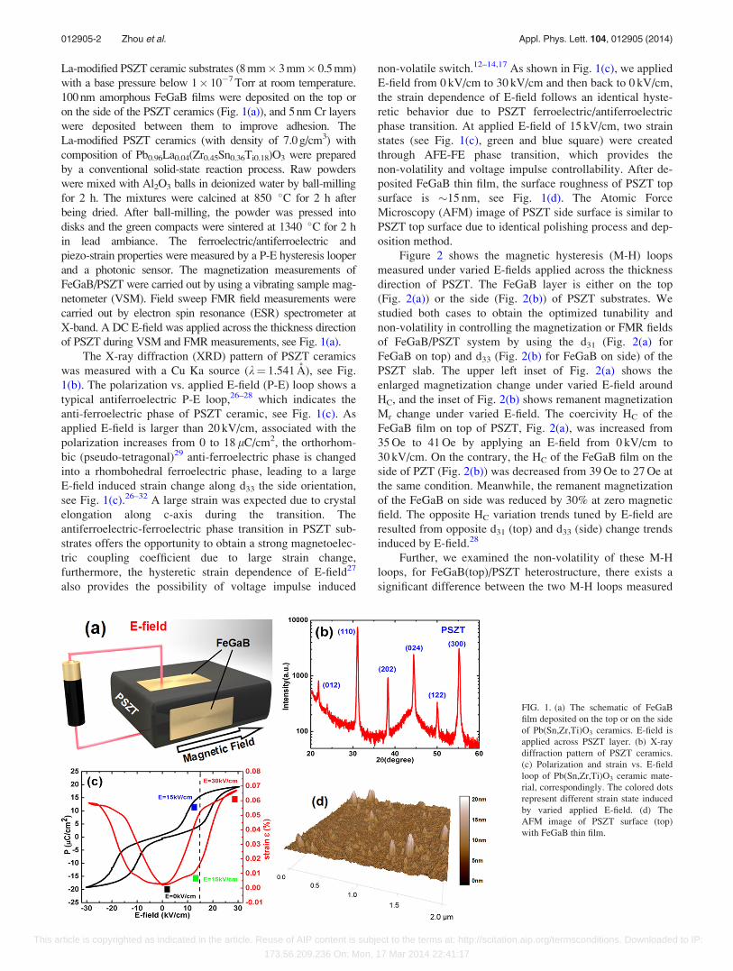
La-modified PSZT ceramic substrates (8 mm� 3 mm� 0.5 mm)
with a base pressure below 1� 10�7 Torr at room temperature.
100 nm amorphous FeGaB films were deposited on the top or
on the side of the PSZT ceramics (Fig. 1(a)), and 5 nm Cr layers
were deposited between them to improve adhesion. The
La-modified PSZT ceramics (with density of 7.0 g/cm3) with
composition of Pb0.96La0.04(Zr0.45Sn0.36Ti0.18)O3 were prepared
by a conventional solid-state reaction process. Raw powders
were mixed with Al2O3 balls in deionized water by ball-milling
for 2 h. The mixtures were calcined at 850 �C for 2 h after
being dried. After ball-milling, the powder was pressed into
disks and the green compacts were sintered at 1340 �C for 2 h
in lead ambiance. The ferroelectric/antiferroelectric and
piezo-strain properties were measured by a P-E hysteresis looper
and a photonic sensor. The magnetization measurements of
FeGaB/PSZT were carried out by using a vibrating sample mag-
netometer (VSM). Field sweep FMR field measurements were
carried out by electron spin resonance (ESR) spectrometer at
X-band. A DC E-field was applied across the thickness direction
of PSZT during VSM and FMR measurements, see Fig. 1(a).
The X-ray diffraction (XRD) pattern of PSZT ceramics
was measured with a Cu Ka source (k¼ 1.541 A), see Fig.
1(b). The polarization vs. applied E-field (P-E) loop shows a
typical antiferroelectric P-E loop,26–28 which indicates the
anti-ferroelectric phase of PSZT ceramic, see Fig. 1(c). As
applied E-field is larger than 20 kV/cm, associated with the
polarization increases from 0 to 18 lC/cm2, the orthorhom-
bic (pseudo-tetragonal)29 anti-ferroelectric phase is changed
into a rhombohedral ferroelectric phase, leading to a large
E-field induced strain change along d33 the side orientation,
see Fig. 1(c).26–32 A large strain was expected due to crystal
elongation along c-axis during the transition. The
antiferroelectric-ferroelectric phase transition in PSZT sub-
strates offers the opportunity to obtain a strong magnetoelec-
tric coupling coefficient due to large strain change,
furthermore, the hysteretic strain dependence of E-field27
also provides the possibility of voltage impulse induced
non-volatile switch.12–14,17 As shown in Fig. 1(c), we applied
E-field from 0 kV/cm to 30 kV/cm and then back to 0 kV/cm,
the strain dependence of E-field follows an identical hyste-
retic behavior due to PSZT ferroelectric/antiferroelectric
phase transition. At applied E-field of 15 kV/cm, two strain
states (see Fig. 1(c), green and blue square) were created
through AFE-FE phase transition, which provides the
non-volatility and voltage impulse controllability. After de-
posited FeGaB thin film, the surface roughness of PSZT top
surface is �15 nm, see Fig. 1(d). The Atomic Force
Microscopy (AFM) image of PSZT side surface is similar to
PSZT top surface due to identical polishing process and dep-
osition method.
Figure 2 shows the magnetic hysteresis (M-H) loops
measured under varied E-fields applied across the thickness
direction of PSZT. The FeGaB layer is either on the top
(Fig. 2(a)) or the side (Fig. 2(b)) of PSZT substrates. We
studied both cases to obtain the optimized tunability and
non-volatility in controlling the magnetization or FMR fields
of FeGaB/PSZT system by using the d31 (Fig. 2(a) for
FeGaB on top) and d33 (Fig. 2(b) for FeGaB on side) of the
PSZT slab. The upper left inset of Fig. 2(a) shows the
enlarged magnetization change under varied E-field around
HC, and the inset of Fig. 2(b) shows remanent magnetization
Mr change under varied E-field. The coercivity HC of the
FeGaB film on top of PSZT, Fig. 2(a), was increased from
35 Oe to 41 Oe by applying an E-field from 0 kV/cm to
30 kV/cm. On the contrary, the HC of the FeGaB film on the
side of PZT (Fig. 2(b)) was decreased from 39 Oe to 27 Oe at
the same condition. Meanwhile, the remanent magnetization
of the FeGaB on side was reduced by 30% at zero magnetic
field. The opposite HC variation trends tuned by E-field are
resulted from opposite d31 (top) and d33 (side) change trends
induced by E-field.28
Further, we examined the non-volatility of these M-H
loops, for FeGaB(top)/PSZT heterostructure, there exists a
significant difference between the two M-H loops measured
FIG. 1. (a) The schematic of FeGaB
film deposited on the top or on the side
of Pb(Sn,Zr,Ti)O3 ceramics. E-field is
applied across PSZT layer. (b) X-ray
diffraction pattern of PSZT ceramics.
(c) Polarization and strain vs. E-field
loop of Pb(Sn,Zr,Ti)O3 ceramic mate-
rial, correspondingly. The colored dots
represent different strain state induced
by varied applied E-field. (d) The
AFM image of PSZT surface (top)
with FeGaB thin film.
012905-2 Zhou et al. Appl. Phys. Lett. 104, 012905 (2014)
This article is copyrighted as indicated in the article. Reuse of AIP content is subject to the terms at: http://scitation.aip.org/termsconditions. Downloaded to IP:
173.56.209.236 On: Mon, 17 Mar 2014 22:41:17

at 15 kV/cm E-field, one(green) is increased from 0 kV/cm,
the other one (blue) is decreased from 30 kV/cm, see Figs.
2(a) and 2(b). This difference of M-H loops at same applied
E-field can be explained by the two strain states at 15 kV/cm
E-field resulting from AFE-FE phase transition, see Fig. 1(c).
With applied bias magnetic field of 40.5 Oe, we switched the
E-field, and the magnetization was changed from 500 G to
�500 G, where DM/M¼ 17%, with non-volatility, see the left
inset of Fig. 2(a). For FeGaB(side)/PSZT heterostructure, see
Fig. 2(b), non-volatile E-field induced M-H loops switching
was also obtained. The largest remanent magnetization switch
back and forth was achieved, corresponding to DM¼ 50 G.
Figs. 2(c) and 2(d) show FMR field spectra of
FeGaB/PSZT multiferroic heterostructure, top and side,
respectively, under varied E-field. The insets of both figures
represent the FMR field dependence of applied E-field.
External magnetic field was applied in plane of FeGaB thin
film (top and side). For FeGaB(top), the maximum FMR field
switch is 32 Oe, from E-field of 0 kV/cm to 30 kV/cm, corre-
sponding to ME coupling coefficient a¼DH/DE¼ 1.1 Oe
cm/kV. For FeGaB(side), the maximum FMR field switch is
81 Oe, leading to large ME coupling coefficient a¼DH/DE
¼ 2.7 Oe cm/kV. The E-field induced in-plane anisotropy field
change can be simulated by piezoelectric and inverse
magneto-elastic equations.11,12 The FMR field Hr dependence
of applied E-field is similar to the hysteric strain dependence
of E-field, see Figs. 1(c) and 1(d) and Figs. 2(c) and 2(d),
which implies non-volatile switch of FMR field. The in-plane
FMR frequency can be expressed by well-known Kittel
equations
f ¼ cffiffiffiffiffiffiffiffiffiffiffiffiffiffiffiffiffiffiffiffiffiffiffiffiffiffiffiffiffiffiffiffiffiffiffiffiffiffiffiffiffiffiffiffiffiffiffiffiffiffiffiffiffiffiffiffiffiffiffiffiffiffiffiffiffiffiffiffiffiffiffiffiffiffiffiffiffiffiffiffiffiffiffiffiffiðHr þ Hk þ Hef f ÞðHr þ Hk þ Hef f þ 4pMSÞ
q; (1)
where c is the gyromagnetic ratio (2.8 MHz/Oe), Hr is the FMR
field, Hk is the in-plane anisotropic field, and 4pMS is the mag-
netization of 1.3 T.13 Heff is compressive and tensile stress
corporately induced internal effective magnetic field. The FMR
field shift DHr can be derived directly from equation
DHr ¼ DHef f ¼3kSeY
MS: (2)
Here, Y is Young’s modulus of 55 GPa and ks is magne-
tostriction of 70 ppm The FMR field shift is directly propor-
tional to the E-field induced effective piezo-strain, where e33
is 0.07% for PSZT slab at applied E-field of 30 kV/cm, see
Figs. 1(c) and 1(d). From Eq. (2), we can calculate effective
magnetic field DHeff¼ 84 Oe for FeGaB(side), which is very
close to our experimental result of 81 Oe. For FeGaB(top), we
have e31� 0.5e33 (Ref. 28) in PSZT ceramics, DHeff¼ 42 Oe,
close to 31 Oe experimental result.
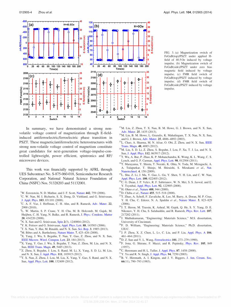
Based on the E-field induced non-volatile switches of
magnetization at bias applied magnetic field and FMR field
in FeGaB/PSZT multiferroic heterostructure, as shown in
Fig. 2, the mechanism of voltage impulse (100 ms) tunable
magnetization and FMR field can be designed. Figs. 3(a) and
3(b) show the voltage impulse tuned FeGaB magnetization
at certain bias magnetic field, by maintaining a constant E-
field of 15 kV/cm, the E-field impulse(<100 ms) with ampli-
tude of �15 kV/cm or 15 kV/cm was applied periodically. In
FeGaB(top)/PSZT heterostructure, see Fig. 3(a), the magnet-
izations were switched between 500 G and �500 G back and
forth at 40.5 Oe applied bias magnetic field. Fig. 3(b) shows
the remanent magnetizations switched back and forth in
FeGaB(side)/PSZT heterostructure induced by voltage
impulses, from 113 G to 50 G. The FMR fields switched by
voltage impulse were also measured. For FeGaB(top)/PSZT
heterostructure, the FMR fields were switched from
�1015 Oe to �995 Oe by voltage impulse, as shown in Fig.
3(c), and the FMR fields were switched from �2094 Oe to
�2043 Oe under the same condition in FeGaB(side)/PSZT
heterostructure, see Fig. 3(d).
FIG. 2. (a) M-H loops under varied E-
field of FeGaB(top)/PSZT multifer-
roics heterostructure. The inset repre-
sents the larged magnetization change
under varied E-field around HC, and
the inset of Fig. 2(b) shows remanent
magnetization Mr change under
varied E-field. (b) M-H loops of
FeGaB(side)/PSZT multiferroics heter-
ostructure. The inset represents rema-
nent magnetization Mr change under
varied E-field. (c) FMR spectra under
varying E-field of FeGaB(top)/PSZT
multiferroics heterostructure. The inset
shows FMR field dependence of E-field.
(d) FMR spectra of FeGaB(side)/PSZT
multiferroics heterostructure. The inset
shows FMR field dependence of E-field.
012905-3 Zhou et al. Appl. Phys. Lett. 104, 012905 (2014)
This article is copyrighted as indicated in the article. Reuse of AIP content is subject to the terms at: http://scitation.aip.org/termsconditions. Downloaded to IP:
173.56.209.236 On: Mon, 17 Mar 2014 22:41:17
In summary, we have demonstrated a strong non-
volatile voltage control of magnetization through E-field-
induced antiferroelectric/ferroelectric phase transition in
PSZT. These magnetic/antiferroelectric heterostructures with
strong non-volatile voltage control of magnetism constitute
great candidates for next-generation voltage-impulse-con-
trolled lightweight, power efficient, spintronics and RF/
microwave devices.
This work was financially supported by AFRL through
UES Subcontract No. S-875-060-018, Semiconductor Research
Corporation, and National Natural Science Foundation of
China (NSFC) Nos. 51328203 and 51132001.
1W. Eerenstein, N. D. Mathur, and J. F. Scott, Nature 442, 759 (2006).2C. W. Nan, M. I. Bichurin, S. X. Dong, D. Viehland, and G. Srinivasan,
J. Appl. Phys. 103, 031101 (2008).3C. A. F. Vaz, J. Hoffman, C. H. Ahn, and R. Ramesh, Adv. Mater. 22,
2900 (2010).4L. W. Martin, S. P. Crane, Y. H. Chu, M. B. Holcomb, M. Gajek, M.
Huijben, C. H. Yang, N. Balke, and R. Ramesh, J. Phys.: Condens. Matter
20, 434220 (2008).5N. X. Sun and G. Srinivasan, Spin 2(3), 1240004 (2012).6Y. K. Fetisov and G. Srinivasan, Appl. Phys. Lett. 88, 143503 (2006).7T. X. Nan, Y. Hui, M. Rinaldi, and N. X. Sun, Sci. Rep. 3, 1985 (2013).8M. Bibes and A. Barthelemy, Nature Mater. 7, 425–426 (2008).9X. Yang, J. Wu, S. Beguhn, T. Nan, Y. Gao, Z. Zhou, and N. X. Sun,
IEEE Microw. Wirel. Compon. Lett. 23, 184 (2013).10X. Yang, Y. Gao, J. Wu, S. Beguhn, T. Nan, Z. Zhou, M. Liu, and N. X.
Sun, IEEE Trans. Magn. 49, 5485 (2013).11Z. Zhou, S. Beguhn, J. Lou, S. Rand, M. Li, X. Yang, S. D. Li, M. Liu,
and N. X. Sun, J. Appl. Phys. 111, 103915 (2012).12T. X. Nan, Z. Zhou, J. Lou, M. Liu, X. Yang, Y. Gao, S. Rand, and N. X.
Sun, Appl. Phys. Lett. 100, 132409 (2012).
13M. Liu, Z. Zhou, T. X. Nan, B. M. Howe, G. J. Brown, and N. X. Sun,
Adv. Mater. 25, 1435 (2013).14M. Liu, B. M. Howe, L. Grazulis, K. Mahalingam, T. X. Nan, N. X. Sun,
and G. J. Brown, Adv. Mater. 25, 4886–4892 (2003).15L. Chao, A. Sharma, M. N. Afsar, O. Obi, Z. Zhou, and N. X. Sun, IEEE
Trans. Magn. 48, 4085 (2012).16M. Liu, S. D. Li, Z. Zhou, S. Beguhn, J. Lou, F. Xu, T. J. Lu, and N. X.
Sun, J. Appl. Phys. 112, 063917 (2012).17T. Wu, A. Bur, P. Zhao, K. P. Mohanchandra, K. Wong, K. L. Wang, C. S.
Lynch, and G. P. Carman, Appl. Phys. Lett. 98, 012504 (2011).18T. Maruyama, Y. Shiota, T. Nozaki, K. Ohta, N. Toda, M. Mizuguchi, A.
A. Tulapurkar, T. Shinjo, M. Shiraishi, S. Mizukami et al., Nat.
Nanotechnol. 4, 158 (2009).19L. Shu, Z. Li, J. Ma, Y. Gao, L. Gu, Y. Shen, Y. H. Lin, and C. W. Nan,
Appl. Phys. Lett. 100, 022405 (2012).20C. G. Duan, J. P. Velev, R. F. Sabirianov, W. N. Mei, S. S. Jaswal, and E.
Y. Tsymbal, Appl. Phys. Lett. 92, 122905 (2008).21H. Ohno et al., Nature 408, 944 (2000).22D. Chiba et al., Nature 455, 515–518 (2008).23T. Zhao, A. Scholl, F. Zavaliche, K. Lee, M. Barry, A. Doran, M. P. Cruz,
Y. H. Chu, C. Ederer, N. A. Spaldin et al., Nature Mater. 5, 823–829
(2006).24J. T. Heron, M. Trassin, K. Ashraf, M. Gajek, Q. He, S. Y. Yang, D. E.
Nikonov, Y. H. Chu, S. Salahuddin, and R. Ramesh, Phys. Rev. Lett. 107,
217202 (2011).25J. Muthukumaran, “Engineering: Materials Science,” M.S. dissertation,
University of Cincinnati.26F. D. William, “Engineering: Materials Science,” Ph.D. dissertation,
UIUC.27J. P. Zhou, X. Z. Chen, L. Lv, C. Liu, and P. Liu, Appl. Phys. A 104,
461–464 (2011).28D. Z. Sun and Y. L. Wang, Ferroelectrics 101, 273–279 (1990).29F. Jona, G. Shirane, F. Mazzi, and R. Pepinsky, Phys. Rev. 105, 849
(1957).30C. Heremans and H. L. Tuller, J. Appl. Phys. 87, 1458 (2000).31Y. Yu and R. N. Singh, J. Appl. Phys. 94, 7250 (2003).32B. V. Hiremath, A. I. Kingon, and J. V. Biggers, J. Am. Ceram. Soc.
66(11), 790–793 (1983).
FIG. 3. (a) Magnetization switch of
FeGaB(top)/PSZT under applied H-
field of 40.5 Oe induced by voltage
impulse. (b) Magnetization switch of
FeGaB(side)/PSZT under zero bias
magnetic field induced by voltage
impulse. (c) FMR field switch of
FeGaB(top)/PSZT induced by voltage
impulse. (d) FMR field switch of
FeGaB(side)/PSZT induced by voltage
impulse.
012905-4 Zhou et al. Appl. Phys. Lett. 104, 012905 (2014)
This article is copyrighted as indicated in the article. Reuse of AIP content is subject to the terms at: http://scitation.aip.org/termsconditions. Downloaded to IP:
173.56.209.236 On: Mon, 17 Mar 2014 22:41:17