strain-resilient electrical functionality in thin-film
TRANSCRIPT

Strain-resilient electrical functionality in thin-film metal electrodes using two-dimensional interlayers
In the format provided by the authors and unedited
Supplementary information
https://doi.org/10.1038/s41928-021-00538-4

1
Supplementary Information
Strain-resilient electrical functionality in thin-film metal electrodes
using two-dimensional interlayers
Chullhee Cho1,4, Pilgyu Kang1,2,4, Amir Taqieddin1, Yuhang Jing3, Keong Yong1, Jin
Myung Kim3, Md Farhadul Haque1, Narayana R. Aluru1,3, and SungWoo Nam1,3*
This PDF file contains:
Supplementary Figure 1‒23
Supplementary Table 1
Supplementary Video Captions 1‒3
Supplementary Notes
Additional References 45-59
2
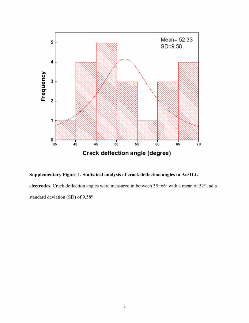
Supplementary Figure 1. Statistical analysis of crack deflection angles in Au/1LG
electrodes. Crack deflection angles were measured in between 35−66o with a mean of 52o and a
standard deviation (SD) of 9.58o.

3
Supplementary Figure 2. Control experiments without an adhesion layer of titanium (Ti) to
verify the role of 2D-interlayer of graphene modulating in-plane facture behaviours. a,
SEM image of 200 nm Au on PDMS substrate without the Ti layer. b, SEM image of 200 nm Cu
on PDMS without the Ti layer. c, SEM image of 200 nm Au on single-layer graphene on PDMS
without the Ti layer. White arrows indicate the bending directions. The distinct in-plane fracture
modes are only apparent with the presence of underlying graphene-interlayer in metal-2D
electrodes regardless of the presence of Ti adhesion layer. Straight cracking with debonding
fracture modes were prominent in electrodes without the graphene-interlayer (a and b), whereas
crack deflection and tortuous cracking were dominant facture modes with the presence of
graphene-interlayer (c).

4
Supplementary Figure 3. Statistical analysis of fracture domain size development with
strain on Au/1LG electrodes. Distribution of fracture domain sizes showed a saturated average
domain size of ~151.6 ± 63.6 𝜇𝑚 at 14% of bending strain.

5
Supplementary Figure 4. Different dominant fracture failure modes and formation of
effective conductive path via crack bridging. a, Straight/debonding fracture failure in bare Au
electrodes. b, Deflected/multiple cracking fractures and the formation of effective conductive
path via crack bridging on polygonal interconnected domains in Au/1LG electrodes. Red circles
indicate crack bridging areas, and a yellow line depicts an exemplary effective conductive path.
c, Magnified SEM images of crack bridging areas.

6
Supplementary Figure 5. High-resolution scanning electron microscopy (SEM) images for
the grain size measurement. a, 200 nm-Au without graphene (uniform grain size of 68.53 ±
1.2 𝑛𝑚). b, 200 nm-Au with graphene (uniform grain size of 49.16 ± 1 𝑛𝑚). c, Single layer
graphene only (the average grain size of graphene of 14.78 ± 1.8 𝜇𝑚).

7
Supplementary Figure 6. Buckle-network formed on as-prepared 200 nm-Au/1LG
electrodes before the onset of fracture. a, 3D view of an AFM topographic scan image of the
Au/1LG electrode. b, Cross-sectional SEM image via focused ion beam sectioning of flat areas
(a blue square in a). Scale bar, 1 m. c, Cross-sectional SEM image of a buckle area (an orange
square in a). Scale bar, 1 m. d, A magnified image of the buckle in c. Scale bar, 500 nm. e,
Topographic height scan and line profile of buckle-network along a-a’ line via AFM analysis. 𝜆
and ℎ are the width and height of the buckles, respectively.
8
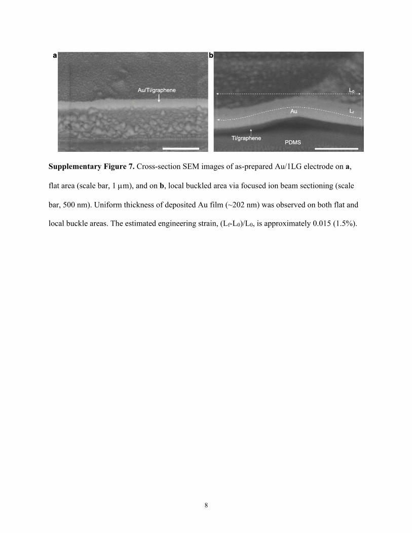
Supplementary Figure 7. Cross-section SEM images of as-prepared Au/1LG electrode on a,
flat area (scale bar, 1 m), and on b, local buckled area via focused ion beam sectioning (scale
bar, 500 nm). Uniform thickness of deposited Au film (~202 nm) was observed on both flat and
local buckle areas. The estimated engineering strain, (Lf-L0)/L0, is approximately 0.015 (1.5%).

9
Supplementary Figure 8. Theoretical study of Gold/Graphene/PDMS electrode under
bending deformation via MD simulation. a, A simulation model structure of
Gold/Graphene/PDMS. Two ends and bottom parts of the film are fixed (enclosed by blue lines).
Neutral plane is marked by a black dash line. b, Adhesion energy of Au/PDMS,
Au/Ti/Graphene/PDMS, and Au/Ti/PDMS. c, Stress-strain curve of multilayer graphene
integrated Au- and bare Au-electrodes, and a mixed 2D-interlayers of MoS2/graphene Au-
electrode. d, Toughness values determined from the stress-strain relationship.

10
Supplementary Figure 9. Molecular dynamics (MD) simulations of buckle-network
formation on a metal film with graphene and the resultant fracture modes under bending
strain. a, Polycrystalline gold with polycrystalline graphene (Au/1LG). b, Formation of buckle
network under bi-axial compressive strain, simulating the thermal residual isotropic compressive
stress occurring during the metal deposition process. c, Straight cracking mode observed on
Au/1LG without buckle-network (top view) under bending strain. d, Local zig-zag cracking
mode observed on Au/1LG with buckle-network (top view) under bending strain, verifying in-
plane crack deflection mechanism (i.e., buckle-guided fracture mechanism) resulting from
buckle-network induced by underlying 2D-interlayer.

11
Supplementary Figure 10. Detailed fracture surfaces on 200 nm-thick Au/1LG electrodes
during bending. a, Schematic illustration of buckle-guided fracture mechanism. b, Progressive
crack development with strain. c, Crack initiation and propagation along buckles. d, Encounter
and interaction between cracks. e, and f, show delaying and limiting complete disconnection via
continuous crack deflection and tortuous cracking.

12
Supplementary Figure 11. Molecular dynamics simulation results showing different
fracture stages/orders of constituent layers of Au with multilayer graphene electrodes
under bending. Au film fractured first during bending, where the intrinsic toughness of Au film
is the lowest and the top surface will experience the maximum tensile stress since the metal film
is located at the furthest from the mechanical neutral plane. Top graphene layer among the 3-
layers of graphene fractured next at a higher strain than the metal film and other underlying
graphene layers fractured subsequently. We note that this simulation did not include buckle-
guide fracture effect.

13
Supplementary Figure 12. Graphene fracture along the crack paths of metal films on
Au/1LG electrodes imaged via scanning electron microscopy. a, Significant charging effects
observed along the Au-film crack edges due to the exposure of the underlying dielectric PDMS
substrate, suggesting the fracture of graphene. b, Fracture surface of graphene after the removal
of the top Au/Ti layer via chemical etching. A relatively white contrast is from the bottom
PDMS substrate. Bending induced wrinkles on graphene were observed along the Au film crack
paths, which were formed due to the resultant compressive strain of Poisson effect, indicating the
fracture of graphene occurred during bending along the crack path of metal.

14
Supplementary Figure 13. Wrinkle vs. buckle-networks formed in 50 nm-thick Au
electrodes before fracture. Top view SEM images of Bare Au (a), and Au/1LG (b). Scale bars,
10 m. AFM topographic height scans and line profiles along a-a’ of conformal wrinkles in the
bare Au (c), and a buckle in the Au/1LG (d).

15
Supplementary Figure 14. Perturbation of crack development in 50 nm-thick bare Au and
Au/1LG electrodes. Detailed SEM images of crack propagation: a, No perturbation (deflection)
by conformal wrinkles formed in bare Au electrodes. b, Perturbation by buckle-network formed
in Au/1LG electrodes.
16
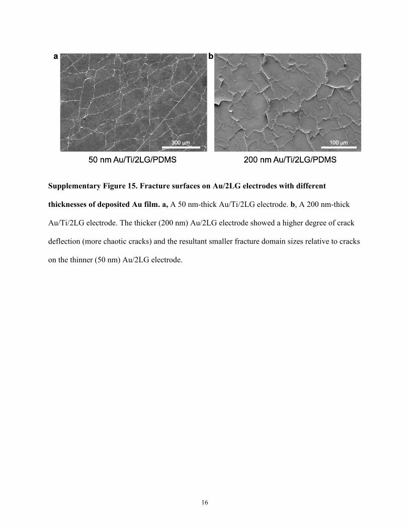
Supplementary Figure 15. Fracture surfaces on Au/2LG electrodes with different
thicknesses of deposited Au film. a, A 50 nm-thick Au/Ti/2LG electrode. b, A 200 nm-thick
Au/Ti/2LG electrode. The thicker (200 nm) Au/2LG electrode showed a higher degree of crack
deflection (more chaotic cracks) and the resultant smaller fracture domain sizes relative to cracks
on the thinner (50 nm) Au/2LG electrode.

17
Supplementary Figure 16. Strain-resilient electrical performance of metal-2D electrodes
integrated with alternative metal and 2D-interlayers. a, Electrically ductile behaviours of Cu-
graphene electrodes as a function of bending strain. b, Electrical failure strain dependent on the
number of graphene-interlayers. c, Electrically ductile behaviours of Au-MoS2 electrodes as a
function of bending strain. d, Electrical failure strain dependent on the number of MoS2-
interlayers. An inset image shows the perspective view of fracture surfaces (multiple cracks with
deflected crack edges without straight cracks on Au/MoS2 area, whereas debonding in Au only
area) during bending. e, Electrically ductile behaviours of Au-hBN electrodes as a function of
bending strain. An inset image shows the perspective view of fracture surfaces (multiple cracks
with deflected crack edges without straight cracks) during bending. f, Electrical failure strain
dependent on the number of hBN-interlayers.
18
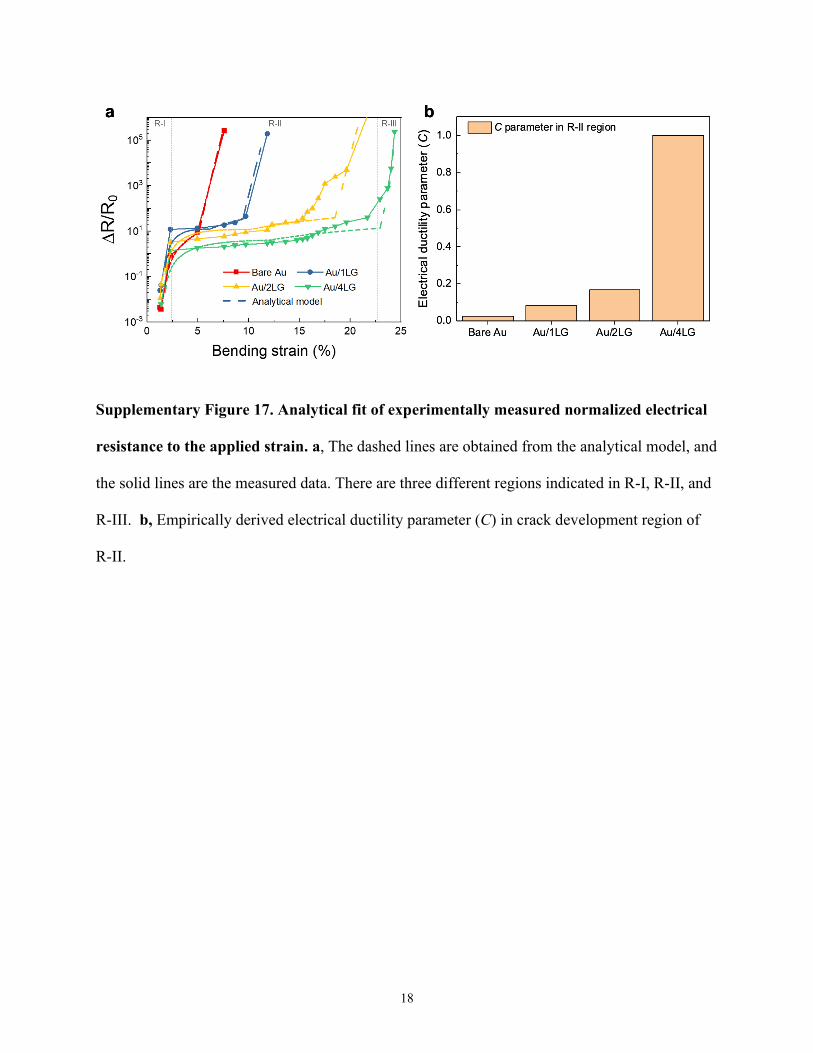
Supplementary Figure 17. Analytical fit of experimentally measured normalized electrical
resistance to the applied strain. a, The dashed lines are obtained from the analytical model, and
the solid lines are the measured data. There are three different regions indicated in R-I, R-II, and
R-III. b, Empirically derived electrical ductility parameter (C) in crack development region of
R-II.

19
Supplementary Figure 18. Experimental adhesion tape test (ASTM D3359-17 pulling test)
results of Au/2LG electrodes. a, An optical image of a separated film from the Au/2LG
electrode by the tape test. Scale bar, 5 mm. b, Raman spectroscopy results on both the separated
film and the substrate, showing the detection of a single layer graphene on both sides. The ratio
of graphene characteristic peaks of 2D-to-G peaks verifies the single layer graphene and,
furthermore, the emergence of D peak indicates defects/dislocations were generated due to the
mechanical peeling test. These results indicate that the delamination could preferably occur
between 2D materials in case of stacked multilayer devices.

20
Supplementary Figure 19. Analytical fit of experimentally measured electrical failure
strains of various metal-2D electrodes as a function of the number of 2D-interlayers.
Exponential decay model (𝜀𝑒𝑙𝑒𝑐𝑡𝑟𝑖𝑐𝑎𝑙 𝑓𝑎𝑖𝑙𝑢𝑟𝑒 = 𝜀𝑒𝑙𝑒𝑐𝑡𝑟𝑖𝑐𝑎𝑙 𝑓𝑎𝑖𝑙𝑢𝑟𝑒,𝑚𝑎𝑥 − 𝐴 ∙ 𝑒𝑥𝑝[−𝐾(𝑥 − 𝑥0)],
where 𝜀𝑒𝑙𝑒𝑐𝑡𝑟𝑖𝑐𝑎𝑙 𝑓𝑎𝑖𝑙𝑢𝑟𝑒,𝑚𝑎𝑥 is the maximum electrical failure strain, 𝑥 is the number of 2D-
interlayers, 𝐴 and 𝐾 are fitting parameters) was employed.
21
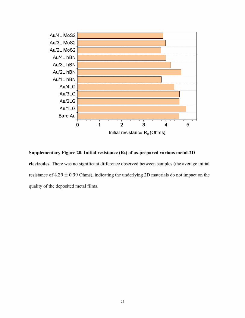
Supplementary Figure 20. Initial resistance (R0) of as-prepared various metal-2D
electrodes. There was no significant difference observed between samples (the average initial
resistance of 4.29 ± 0.39 Ohms), indicating the underlying 2D materials do not impact on the
quality of the deposited metal films.

22
Supplementary Figure 21. Schematic illustration of luminous power measurements.
Flexible light emitting devices include a conventional metal-based and a metal-2D based
interconnector.

23
Supplementary Figure 22. Luminous power measurement of a flexible light emitting device
integrated with an Au/2LG interconnector upon bending cyclic test. a, Luminous power
during 500 bending (i.e., strained, blue squares)-relaxed (red squares) cycles at a 3% bending
strain. We observed about 3.97% luminous power reduction after 500 cycles. An inset plot shows
the continuous change in luminous power upon bending application. b, Uniformity test by 3x3
point measurement (a pixel size of 9.5 mm). We observed a variance of ±1.2% with the average
luminous power of 31.7 W and standard deviation of 0.38 W.

24
Supplementary Figure 23. Optical characterization of the transferred multilayer graphene
on PDMS substrates. a, Optical transmittance of stacked multilayer of graphene via UV-Vis
spectroscopy. b, Raman spectra of graphene transferred on PDMS substrates with multiple
transfers of graphene layers and a bare PDMS substrate. c, The full-width at half-maximum of
2D peak and the intensity ratio of 2D-to-G peaks on transferred multilayer graphene on PDMS
substrates.

25
Supplementary Table 1. Results of adhesion test performed based on ASTM D3359-17
evaluation method.
Au only
Au/Ti
(Cu/Ti)
Au/Ti/1LG
(Cu/Ti/1LG)
Au/Ti/2LG
(Cu/Ti/2LG)
Gr only
ASTM D3359-17 0A 4A (3A) 0A (0A) 0A (0A) 0A
Scotch tape - + - * -
Evaluation criteria
5A No peeling or removal
4A Trace peeling or removal along incisions or at their intersection
3A Jagged removal along incisions up to 1.6 mm on either side.
2A Jagged removal along most of incisions up to 3.2 mm on either side
1A Removal from most of the area under the tape
0A Removal beyond the area of the X
+, deadhesion at the tape–metal interface
–, deadhesion at the metal (or graphene)–PDMS interface
*, deadhesion at the graphene-graphene interface

26
Supplementary Video Captions
Supplementary Video 1. Crack development in a bare Au electrode under bending deformation.
Supplementary Video 2. Crack development in an Au/1LG electrode under bending
deformation.
Supplementary Video 3. Practical functionality demonstration of flexible light emitting devices
integrated with a conventional thin metal film based interconnector and a metal-2D based
interconnector.
27
Supplementary Notes
Grain size and metal film quality characterization
To investigate grain size influence on fracture behaviours, we first characterized the grain sizes
of 200 nm gold (Au) film with and without graphene on PDMS. As shown in high-resolution
scanning electron microscope (SEM) images, the uniform grain size of 68.53 ± 1.2 𝑛𝑚 was seen
on 200 nm-thick Au without graphene (Supplementary Fig. 5a) and the uniform grain size of
49.16 ± 1 𝑛𝑚 was observed on 200 nm-thick Au with graphene (Supplementary Fig. 5b). It has
been also reported that less than 7.2% difference of Au grain size was observed from 25 nm-
thick Au films deposited on monolayer graphene (mean crystallite size of 22.3 nm) and 25 nm-
thick Au films without graphene (23.9 nm)45. Thus, the quality of Au thin film did not show
significant difference between bare Au and Au/graphene (Au/1LG) in terms of the grain size. We
next characterized the grain size of our CVD-grown graphene. As shown in Supplementary
Figure 5c, the average grain size of graphene was 14.78 ± 1.8 𝜇𝑚. These results show that there
is no strong/direct correlation between the grain size and fracture domain size where the
measured grain sizes of Au without graphene (68.53 ± 1.2 𝑛𝑚) and Au with graphene (49.16 ±
1 𝑛𝑚) are both at least three orders-of-magnitude smaller than the average fracture domain size
(~151.6 ± 63.6 𝜇𝑚, Fig. 2d) on the Au with graphene electrode (Au/1LG) and the grain size of
graphene (14.78 ± 1.8 𝜇𝑚) is at least an order-of-magnitude smaller than the average fracture
domain size. We also characterized deposited metal film quality on graphene in terms of
deposition uniformity. Both cases of metals on PDMS and metals on graphene follow a dominant
growth mode of the well-known Volmer-Weber model of thin films growth due to the
sufficiently small adsorption energy of both metal adatoms on graphene and metal adatoms on
PDMS45. The cross-section SEM images of Au/1LG sample via focused ion beam sectioning of

28
flat (Supplementary Fig. 7a) and along buckle-network regions (Supplementary Fig. 7b) verified
the uniformity of deposited Au film (~202 nm) on graphene. We note that the estimated
engineering strain (~(Lf-L0)/L0) is approximately 0.015 (1.5%), which is much less than the
applied bending strain in our experiment, indicating the deformation tolerance by buckling is not
substantial. Lastly, we examined the quality of deposited metal films in terms of electrical
characteristics by comparing initial electrical resistance of various as-prepared samples
(Supplementary Fig. 20). There was no significant difference between samples (the average
initial resistance of 4.29 ± 0.39 Ohms), indicating the underlying 2D-interlayers do not impact
on the subsequent deposited metal film quality. Any other factors that might influence the crack
generation besides applied strain may be 1) thickness of film, which is strongly related to the
intrinsic fracture toughness of the film, 2) strain rate where our tested strain rate is close to the
quasi-static loading and comparable with reported strain rate for wearable sensor tests46,47 and 3)
other environmental factor including humidity.
Modification of mechanical properties of the metal film via the insertion of graphene-
interlayers
MD simulation results (Supplementary Fig. 8) show that the insertion of graphene-interlayer led
to an increase in effective modulus and toughness, and a decrease in adhesion energy (~0.20847
J∙m-2) compared to the Au/Ti/PDMS case (~0.2399 J∙m-2). However, the adhesion of Au/Ti/1LG
is still much stronger than the Au/PDMS case (~0.09422 J∙m-2) where interfacial debonding
failures often occur. It has been studied that tuning the adhesion of metals on soft substrates can
significantly improve mechanical robustness of the system for flexible and wearable
electronics48,49. Our experimental and theoretical results suggest that our 2D-interlayer

29
engineering approach achieves the desired adhesion regime where we can enhance the
electromechanical robustness of the flexible electrodes and prevent a catastrophic fracture failure
mode of film debonding from the substrate under various deformations. In particular,
Au/Ti/PDMS case showed the earlier debonding fracture failure of the film at a smaller strain
compared to the Au/Ti/1LG/PDMS case as shown in Figure 2a and Supplementary Figure 4.
Early saturation of the fracture domain size on bare Au (~7% in Fig. 2d) suggests there is no
further strain energy dissipation by cracking and thus the excess strain energy will be dissipated
through interfacial fracture50 resulting in early film debonding failure, whereas continuous
decrease in the domain size of Au/1LG (until 14% in Fig. 2d) implies prolonged energy
dissipation by progressive cracking and thus significantly delaying the film debonding. The
modification of adhesion energy was also corroborated by experimental adhesion test based on
the ASTM Standard D3359-17 taping test. Five types of samples (Au only, Au/Ti, Au/Ti/1LG,
Au/Ti/2LG, Graphene only on PDMS substrates) were tested right after the completion of metal
deposition and the results are summarized in Supplementary Table 1. Interestingly, for the
Au/Ti/2LG case, de-adhesion occurred at the graphene/graphene interface, which was confirmed
by detection of single layer graphene on both substrate and the separated film via Raman
spectroscopy (Supplementary Fig. 18). The ratio of graphene characteristic peaks of 2D-to-G
peaks verifies the single layer graphene and, furthermore, the emergence of D peak indicates
defects/dislocations were generated due to the mechanical peeling test. This indicates that there
will be an additional energy dissipation from interlayer sliding in the case of multilayer 2D
interlayers, contributing to the dependence of electromechanical enhancement on the number of
2D-interlayers as discussed in Figure 3. All these modifications including increase in the
effective modulus and decrease in the adhesion (Supplementary Fig. 8 and Supplementary Table

30
1) led by 2D-interlayers are likely to induce spontaneous buckles under the inevitable isotropic
compressive strain produced by built-in strain due to thermal expansion mismatch
(Au=14×10−6∙K-1, PDMS=960×10−6∙K-1) after the metal deposition15. In addition, our MD
simulation results (Supplementary Fig. 9a,b) revealed that buckle-network of metal/graphene can
be formed favorably along the grain boundaries of polycrystalline graphene due to their relative
weakness to the basal plane under the emulated isotropic compressive strain. Our observation
that interfacial engineering with the 2D-interlayers enables formation of buckle-network agrees
well with previously reported simulation results51. When the interfacial toughness (i.e., adhesion)
is high (e.g., bare Au), the Au film evolves into homogenous herringbone or labyrinth surface
wrinkle patterns51 (Supplementary Fig. 13a), whereas with a lower interfacial toughness (e.g.,
Au/1LG) and a higher film/substrate modulus ratio, Au/1LG films develops into buckle-
delamination network (Supplementary Fig. 13b).
Crack growth perturbation by buckles vs. conformal wrinkles
To further investigate crack growth perturbation by 2D-interlayer induced buckle-network, we
prepared electrodes with much thinner (50 nm) Au electrodes. After metal deposition, buckle-
delamination and homogeneous conformal wrinkle-network were distinctly seen on the as-
prepared Au/1LG and bare Au electrodes, respectively (Supplementary Fig. 13). We observed
that cracks preferentially initiated at the crest of the buckles and propagated along the
heterogenous buckle-network (Supplementary Figs. 10 and 14). We determined the maximum
uniaxial tensile strain (𝜀) accumulated on crest of the buckles by 𝜀~𝜋2𝑡ℎ/(1 − 𝜎2)𝜆2 52, where t
is the thickness of the metal film, 𝜎 is Poisson’s ratio, and ℎ and 𝜆 are the height and width of the
buckles, respectively, which we extracted from the AFM topographic scan results

31
(Supplementary Figs. 6 and 13). The estimated maximum tensile strain 𝜀 accumulated on top of
the buckles ranges from 1.1% to 1.3%. This suggests that the crest of buckle is much more
susceptible for the crack initiation due to the built-in localized strains at the crest, compared to
the planar surface. Our MD simulation results (Supplementary Fig. 9d) also revealed crack
initiated at the crest of buckle under bending strain and showed crack propagated with local zig-
zag fluctuation. A previous experimental study53 where buckles were intentionally created with
prestrain on iron film/PDMS reported that the positions of all the cracks were coincident with the
location of buckles after applying tensile strain. This previous result agrees well with our
coincident buckle-crack location observation and implies a coupling between buckle and
fracture. We also observed that cracks were perturbed/deflected by the buckle-network domains
during the dynamic fracture process in Au/1LG electrodes, whereas single cracks grew
unperturbed by the densely packed wrinkle-network domains in bare Au electrodes
(Supplementary Fig. 14). Thus, in addition to the effect of localized strain at buckle crests, we
also attribute the crack perturbation of buckle-network to discreteness of buckle-network
compared to semi-continuous distribution of conformal wrinkle-network (Supplementary Figs.
13 and 14). More detailed parametric studies on the discreteness of buckles may provide
potential engineering design parameters for the improvement of electromechanical robustness of
thin metal film based electrodes. As a summary, we can explain the crack generation mechanism
in 4-steps which are applicable to thin film metals (relatively ductile) on a flexible elastomeric
substrate-based system:
1) Spontaneous buckle-network formation (Supplementary Figs. 6, 7, and 9a,b) on the as-
prepared electrode after the metal deposition51 owing to 1a) thermal residual compressive stress
by the different thermal expansion coefficients of the constituent materials15, and 1b) reduced

32
film adhesion and increased effective modulus modulated by the insertion of 2D-interlayers
(Supplementary Fig. 8, Supplementary Table 1, and Supplementary Note 2).
2) Upon bending, multiple cracks favorably initiate at the crest (top) of the formed buckles
because of the built-in localized strain at the crest (~1.1-1.3%, Supplementary Figs. 6 and 13)
leading to the susceptibility for the crack initiation compared to other (i.e., non-buckled) areas53.
3) Cracks propagate with local zig-zag fluctuations because of the tortuous geometry of the
buckle-network (Supplementary Figs. 9c,d and 14b), analogous to crack kinking under mixed-
mode loading23.
4) Interaction between cracks deflect/perturb crack extension, delaying the complete
disconnection across the entire film (Supplementary Fig. 10).
Overall, we can deduce that buckles can effectively provide low-energy routes as strain-relief
paths, guiding the crack propagation and further perturbation, resulting in limited crack
extensions. Thus, beyond the most common fracture modes of intragranular/intergranular crack
extension along grain boundaries of constituent materials54, extrinsic toughening mechanisms of
continuous crack perturbation with crack bridging led by 2D-interlayer is further effective in
resisting crack extension to a complete disconnection, allowing the enhanced electrical
robustness of flexible electrodes.
Analytical model of electrical ductility
The electrical resistance, 𝑅, under crack propagation can be expressed as a function of the
applied strain, 𝜀, as follows28:

33
𝑅(𝜀) = 𝑅𝑜 + ∑ 𝑅𝑖(𝜀)
𝑘
𝑖=1
(3)
where 𝑅o is the electrical resistance of the crack-free surface, 𝑅𝑖 is strain-dependent electrical
resistance of crack 𝑖, and 𝑘 is the number of cracks in the material at strain 𝜀. To establish an
analytical model describing the electrical ductility, we need to assume there exist effective
conducting paths throughout surface cracks, which is closely related to the experimental
observation of crack bridging discussed earlier. We employed the model developed by Leterrier
et al.28, which assumed the existence of a conducting path during fragmentation damage in
conductive coatings (e.g., indium tin oxide or carbon nanotube) on PDMS substrate under tensile
loading. The electrical resistance was expressed in terms of the generated cracks as28:
𝑅(𝑘) = 𝑅0 + 𝜌𝑐 ×𝜆0
𝑡𝑊
1
𝐴𝑙𝑛 {
(𝑁 − 1)!
(𝑁 − 𝑘)𝑘(𝑁 − 𝑘 − 1)!} (4)
where 𝜌𝑐 is the resistivity of the crack, 𝜆o is a scaling factor which relates the crack opening to
the applied strain, 𝑡 and 𝑊 are the crack thickness and length, respectively, 𝐴 is an adjustable
factor which relates the crack propagation rate to Weibull modulus28, and 𝑁 is the number of
cracks at the saturation of the cracking process, which contains a conceptual analogy to
percolation threshold accounting for the formation of conductive paths in metal nanowire
percolation network55. We note that our metal-2D electrodes showed lower sheet resistance
compared to the metal nanowire percolation network55, where we intended to maintain/utilize
intrinsically high conductivity of metals. Next, changes in the normalized electrical resistance,
Δ𝑅/𝑅o=[𝑅(𝑘) − 𝑅o]/𝑅o, can be derived from equation (4) as:
Δ𝑅
𝑅o=
1
𝐶(𝑘)×
λ0
𝑅𝑜𝑙𝑛 {
(N − 1)!
(N − k)k(N − k − 1)!}
(5)

34
where, in our case, 𝐶 is an electrical ductility parameter, which is an empirically derived variable
that relates the progressive increase in the number of cracks to the normalized change in the
electrical resistance. It is important to recognize that 𝐶(𝑘) = 𝑓(ρc, t, W, 𝐴, 𝑘) is a function of
several quantities. For example, the value of crack propagation rate, which relates to 𝐴
parameter, will vary with fracture state and result in change in the value of C during the
dynamic crack development. The number of cracks, 𝑘, can be expressed in terms of the applied
strain using statistical distribution as28:
𝑘(𝜀) = 𝑁 × (1 − exp[−𝐴(𝜀 − 𝜀crit)]) (6)
where 𝜀crit is a mechanical critical strain. We can see that as the parameter 𝐴 increases, the
number of cracks before failure increases at a given critical strain. Equation (5) can predict the
change of electrical resistance for a given 𝑘 that corresponds to an applied strain as given in
equation (6). Using equations (5) and (6), the experimental measurements can be fitted to relate
the change in the resistance to the applied strain due to the progressive cracking. In the fitting,
we set 𝜀crit equals to 2% which corresponds to the critical strain of the gold (assuming gold is the
first material to fail). Our experimental results of the change in electrical resistance for all
electrodes (Supplementary Fig. 17a solid lines) showed that there is a sudden jump in a small
strain (< 3%) with approximately the same slope in electrical resistance change due to the crack
initiation upon strain regardless of the insertion of graphene-interlayers. This suggests that we
can assume the gold is the first material to fracture (i.e., crack initiation). We note that the
increase in the intrinsic fracture toughness (Supplementary Fig. 8d) with the graphene-interlayers
is partly responsible for the increased capability of metals with indigenous cracks to resist crack
extension by absorbing energy, resulting in the delayed crack propagation compared to bare
metal, but not for the crack initiation. We also assume a saturated number of cracks per unit

35
length (i.e., crack density) of 𝑁= 148 mm−1 as this number has been experimentally measured
for the graphene-interlayers integrated gold electrodes. Supplementary Fig. 17a (dotted line)
shows the analytical resistance change as a function of strain obtained using equations (5) and
(6) with comparisons to the corresponding experimentally measured data. The fit shows that the
value of the empirical variable 𝐶 is characterized by three regions. In the first region (e.g., R-I
for Au/4LG in Supplementary Fig. 17a), where the cracks are initiated around a strain of 2%, we
see a jump in the electrical resistance associated with a fall in the value of 𝐶. The second region
(R-II) lies between the first jump in the electrical resistance and the third region (R-III) where a
complete failure of the material occurs results in a dramatic increase in the electrical resistance.
In the R-II region, the progressive cracking due to the presence of the graphene-interlayers
results in a gradual and stable crack development and therefore the change in the resistance is
within 10%56. This region can be viewed as a resistance locking region by the graphene-
interlayer in which the value of 𝐶 changes slowly with the strain. Fitting for the R-II region
shows that the electrical ductility parameter of 𝐶 increased by more than a factor of 3 for
Au/1LG, and by a factor of 40 for Au/4LG compared to that of bare Au, as shown in
Supplementary Fig. 17b. The increase in the value of 𝐶 can be associated largely with the
increase in the value of crack propagation rate related parameter (𝐴) in addition to the value of
crack geometry related parameters (ρc, t, W). The physics of the increase in 𝐶 is attributed to the
presence of delaminated buckle-network upon adding graphene. With the introduction of
graphene-interlayers, (i) increase in intrinsic fracture toughness (Supplementary Fig. 8d) and (ii)
in-plane fracture perturbation (e.g., crack deflection and perturbation) by buckle-network
(Supplementary Fig. 14) are two dominant mechanisms decreasing the crack propagation rate
(i.e., increase in parameter A and thus increase in parameter 𝐶) leading to more stable and

36
gradual crack development. We also note that there could be minor contributing factors including
an additional energy dissipation resulting from the interlayer-sliding between 2D-interlayers29
that can reduce the effective strain energy the top metal film would experience under a higher
strain. Overall, the increase in the value of 𝐶 results in a higher electrical ductility as the number
of graphene-interlayer increases due to the increase in the number of cracks that the materials
can withstand before failure.
Characterization of multilayer configuration
Prior to the metal deposition, we analysed the quality of the transferred graphene and the number
of stacked graphene layers on PDMS substrates by two non-destructive optical analysis
techniques: UV-Vis spectroscopy (Supplementary Fig. 23a) and Raman spectroscopy
(Supplementary Fig. 23b). This is to explore the integrity of multi 2D-interlayer configuration
prior to subsequent metal deposition to ensure there was no significant defects and chemical
residues that may induce undesired fracture behaviours. The transmittance value from each
sample was normalized by the transmittance of the underlying PDMS substrate measured on the
same sample. The number of transferred graphene layers was determined from the normalized
transmittance at a wavelength of 550 nm using equation (7)57.
𝑇(%) = (1 + 1.13𝜋𝛼𝑁 2⁄ )−2, 𝛼1/137 (fine-structure constant) (7)
Based on the weak optical absorptivity (~2.3%) of single-layer graphene58, the observation of
discrete transmittance increments (Supplementary Fig. 23a) clearly shows that we obtained a
deterministic number of graphene layers using our laminated stamping transfer method. The
Raman spectroscopy analysis shown in Supplementary Fig. 23b also verified the different
number of graphene layers. Changes in the intensity ratio between G (~1580 cm-1) and 2D

37
(~2650 cm-1) peaks provide evidence for a multilayer graphene configuration. The negligible
intensity of the D peak from the graphene layer at roughly 1350 cm-1 indicates that our transfer
method causes no significant damage/defect on graphene layers. Peaks at roughly 1250 cm-1 and
slightly above 1400 cm-1 are from the underlying PDMS substrates. In addition to the relative
intensity ratio of 2D-to-G peaks for multilayer configuration analysis, the most prominent
difference in the spectra of single layer and few-layers lies in the 2D peak59. Because of the band
splitting into subpeaks (𝜋 and 𝜋∗ bands splitting) in case of a good interlayer coupling (i.e., close
contact between graphene layers), the full-width-half-maximum (FWHM) of 2D peak increases
as the number of layers increases as shown in Supplementary Figure 23c.
Additional references
45. Yakubovsky, D. I. et al. Graphene-supported thin metal films for nanophotonics and
optoelectronics. Nanomaterials 8, 1058 (2018).
46. Pan, S. et al. A highly stretchable strain sensor based on CNT/graphene/fullerene-SEBS.
RSC Adv. 10, 11225–11232 (2020).
47. Tolvanen, J., Hannu, J. & Jantunen, H. Stretchable and Washable Strain Sensor Based on
Cracking Structure for Human Motion Monitoring. Sci. Rep. 8, 13241 (2018).
48. Guo, C. F. et al. Fatigue-free, superstretchable, transparent, and biocompatible metal
electrodes. Proc. Natl. Acad. Sci. 112, 12332–12337 (2015).
49. Sun, Y., Choi, W. M., Jiang, H., Huang, Y. Y. & Rogers, J. A. Controlled buckling of
semiconductor nanoribbons for stretchable electronics. Nat. Nanotechnol. 1, 201–207
(2006).
38
50. Li, T. et al. Delocalizing strain in a thin metal film on a polymer substrate. Mech. Mater.
37, 261–273 (2005).
51. Pan, K., Ni, Y., He, L. & Huang, R. Nonlinear analysis of compressed elastic thin films on
elastic substrates : From wrinkling to buckle-delamination. Int. J. Solids Struct. 51, 3715–
3726 (2014).
52. Castellanos-Gomez, A. et al. Local strain engineering in atomically thin MoS2. Nano Lett.
13, 5361–5366 (2013).
53. Gao, T., Sun, Y., Feng, Y. & Yu, S. Morphological evolutions of iron films on PDMS
substrates under uniaxial compression / tension. Philos. Mag. 96, 2943–2952 (2016).
54. Ritchie, R. O. The conflicts between strength and toughness. Nat. Mater. 10, 817–822
(2011).
55. Lee, P. et al. Highly stretchable and highly conductive metal electrode by very long metal
nanowire percolation network. Adv. Mater. 24, 3326–3332 (2012).
56. Leterrier, Y. et al. Mechanical integrity of thin inorganic coatings on polymer substrates
under quasi-static, thermal and fatigue loadings. Thin Solid Films 519, 1729–1737 (2010).
57. Zhu, S. E., Yuan, S. & Janssen, G. C. A. M. Optical transmittance of multilayer graphene.
EPL 106, 17007 (2014).
58. Nair, R. R. et al. Fine structure constant defines visual transparency of graphene. Science
320, 1308 (2008).
59. Graf, D. et al. Spatially resolved raman spectroscopy of single- and few-layer graphene.
Nano Lett. 7, 238–242 (2007).