step stencil technology - smt stencils, circuit board...
TRANSCRIPT

Step Stencil Technology
Greg Smith
Tony Lentz

Outline/Agenda
Introduction
Step Stencils Technologies
Step Stencil Design
Printing Experiment
Experimental Results
Future Work
Acknowledgements
Q & A

Introduction
1.1.7 Relief Etch Also
known as Etch Relief and
Under Etch. Adding an under
etch of the foil to create a
pocket for raised features,
labels, or a mulit-print
function.
1.1.22 Step Stencil A Stencil
with more than one foil
thickness level.
*IPC 7525B, “Stencil Design Guidelines”, 2011-October.
Introduction
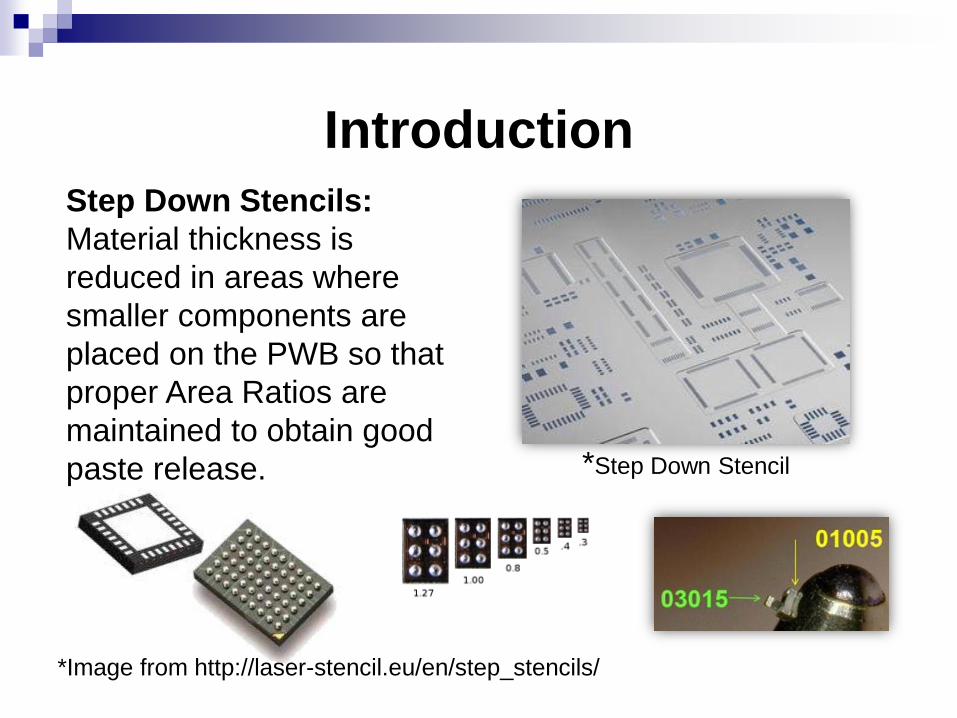
Step Down Stencils:
Material thickness is
reduced in areas where
smaller components are
placed on the PWB so that
proper Area Ratios are
maintained to obtain good
paste release.
*Image from http://laser-stencil.eu/en/step_stencils/
*Step Down Stencil

Introduction
Step UP Stencils:
Material thickness is
increased around specific
components such as edge
connectors, large BGA’s,
D-PAK’s and other devices
to increase the volume of
paste deposited.Step Up Stencil

Step Stencil Technologies
Currently there are three technologies
in the U.S. to manufacture step
stencils.
Welded Technology
Etched Technology
Micro-Machined Technology

Step Stencil Technologies
Photo-Chemical Etching
• Historically, the primary
method to manufacture step
stencils
• Photographic process
applies resist to areas that
will not be etched.
• Etchant is sprayed onto
surface and removes
material until the desired
thickness is achieved.
Etched Technology

Step Stencil Technologies
Laser Welded Technology
• The area of the step is cut
from the stencil.
• The required thickness of the
step area is cut from another
foil the exact same size.
• The new foil blank is placed
into the cut out area and the
foil is welded together.
• Apertures are then laser cut.
Laser Welded Technology

Step Stencil TechnologiesMicro-Machining Technology
• Material is attached to cooled
vacuum plate.
• CNC based milling machine
removes very small amounts
of material at a time until
desired thickness is
achieved.
• Stepped foil is mounted to
frame and apertures are
laser cut.
Laser Welded Technology

Step Stencil Design
• Base stencil thickness 4 mils
(101.6 microns)
• Step Pocket Depths
(Foil Thickness)
• 3.5 mils (88.9 microns)
• 3.0 mils (76.2 microns)
• 2.5 mils (63.5 microns)
• 2.0 mils (50.8 microns)
• Each step area was 1 inch
square (25.4 mm) and the step
design is shown here.
The 3.5 Mil Step Pocket (.5 mil step depth) was not used in this paper.

Printing Experiment
Apertures were created for
the following components:
• 03015 Metric
• 01005
• 0.3 mm BGA
• 0.4 mm BGA
• 0.5 mm pitch QFNs.
Apertures were cut at
varying distances from the
step edges:
10, 20, 30, 40, and 50 mils.

Printing Experiment
Data was collected after printing 10 boards with each stencil. The effects of the
FPN coating were compared to the uncoated part of the stencil on printing of
solder paste.
Fluoro-Polymer Nano (FPN) coating

Printing Experiment
A 10 print study was run on each step stencil using a popular no clean,
SAC305 Type 4 solder paste. The circuit boards used were bare copper clad
material 0.062” (1.57 mm) thick.
Step Stencil Contact Side with FPN Nano-Coating.

Equipment
Parameter Value
Squeegee Length 300 mm
Squeegee Pressure 0.18 kg/cm (5.4 kg)
Squeegee Speed 30 mm/sec
Squeegee Angle 60 degrees
Separation Speed 1.0 mm/sec
Cleaning Cycle W/V/D every print
Cleaning Solvent Isopropanol (IPA)
Solder Paste NC SAC305 T4

Stencil Thickness Measurements
Step
Thickness
(mils)
Step
Depth
(mils)
Etched –
Depth /
STDev
(mils)
Welded -
Depth /
STDev
(mils)
Machined -
Depth /
STDev
(mils)
2.0 2.0 2.36 / 0.11 2.08 / 0.19 2.01 / 0.17
2.5 1.5 1.69 / 0.16 1.60 / 0.18 1.25 / 0.15
3.0 1.0 1.15 / 0.19 0.97 / 0.18 1.08 / 0.17
• Chemical etching process created deeper step downs
than the nominal value
• Welding and Micro-Machining processes created steps
that are closer to the target depth.
• Overall, the standard deviations are very similar for each
technology.

Printing Results
Solder Paste Volumes for the 3.0 mil Etched Step.
Etched Step

Printing Results
Solder Paste Volumes for the 2.5 mil Etched Step.
Etched Step

Printing Results
Solder Paste Volumes for the 2.0 mil Etched Step.
Etched Step

Printing Results
Tukey-Kramer HSD Analysis for the FPN Coated, Etched 3.0 mil
Step (1 mil step down) and the 9.8 x 35.4 Aperture.
Etched Step

Printing Results
The printed solder paste volume is higher for the 10 and 20 mil
distances than the 50 mil distance.
Level Mean
10 A 839.52500
20 A 823.35000
40 A B 798.30000
30 A B 796.65000
50 B 776.22500
Tukey-Kramer HSD Analysis for the FPN
Coated, Etched 3.0 mil Step(1 mil step down)
and the 9.8 x 35.4 Aperture.
Etched Step

Printing Results
The printed solder paste volume is higher for the 10 and 20 mil
distances than the 50 mil distance for the 9.8 x 35.4 mil apertures but
smaller aperture volumes seem to be consistent from 10 – 50 mils
from the step edge.
Etched Step
8 x 9 mil AperturesPaste w/ blue U.V. dye added

Printing Results
Solder Paste Volumes for the 3.0 mil Welded Step.
Welded Step

Printing Results
Solder Paste Volumes for the 2.5 mil Welded Step.
Welded Step
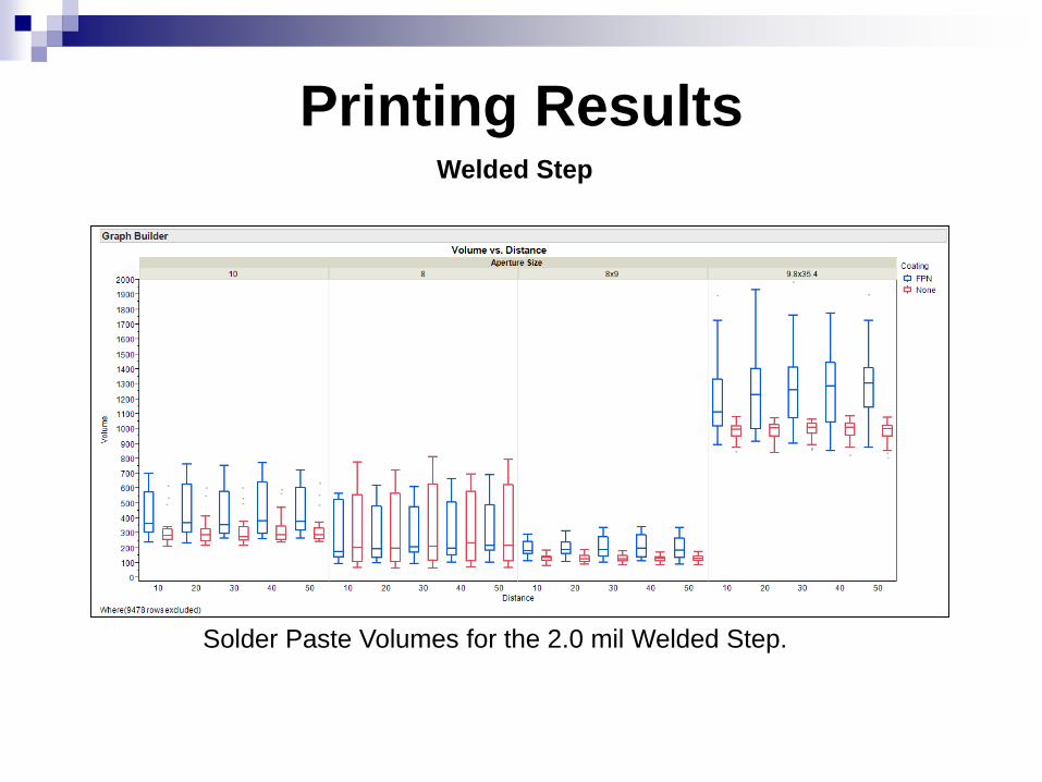
Printing Results
Solder Paste Volumes for the 2.0 mil Welded Step.
Welded Step

Printing Results
Tukey-Kramer HSD Analysis for the Uncoated, Welded 2.5 mil Step
and the 9.8 x 35.4 Aperture.
Welded Step

Printing Results
Paste volume at the 10 mil distance is significantly higher than the
40 and 50 mil distances. Paste volume is significantly higher at the
20 mil distance than then 50 mil distance.
Welded Step
Level Mean
10 A 1015.3250
20 A B 988.8000
30 A B C 954.1750
40 B C 916.4750
50 C 891.8500
Connecting Letters Report
Tukey-Kramer HSD Analysis for the Uncoated,
Welded 2.5 mil Step and the 9.8 x 35.4 Aperture.

Printing Results
The printed solder paste volume is higher for the 10 and 20 mil
distances than the 50 mil distance for the 9.8 x 35.4 mil apertures but
smaller aperture volumes seem to be consistent from 10 – 50 mils
from the step edge.
Welded Step
8 x 9 mil AperturesPaste w/ blue U.V. dye added

Printing Results
Solder Paste Volumes for the 3.0 mil Micro-Machined Step.
Micro-Machined Step

Printing Results
Solder Paste Volumes for the 2.5 mil Micro-Machined Step.
Micro-Machined Step

Printing Results
Solder Paste Volumes for the 2.0 mil Micro-Machined Step.
Micro-Machined Step

Printing Results
Tukey-Kramer HSD Analysis for the Uncoated, Machined 2.0 mil Step (2 mil
step down) and the 8 x 9 Aperture.
Micro-Machined Step

Printing Results
Printed solder paste volume is significantly higher at the 10 and 20
mil distances than the 30, 40, and 50 mil distances. This is also
true for the 9.8 x 35.4 mil aperture with 2.0 mil and 2.5 mil machined
step thicknesses.
Micro-Machined Step
Connecting Letters Report
Tukey-Kramer HSD Analysis for the Uncoated, Micro-Machined
2.0 mil Step (2 mil step down) and the 8 x 9 Aperture.
Level Mean
10 A 116.82500
20 A 113.92500
40 B 104.20000
30 B 103.72500
50 B 101.42500

Printing Results
The printed solder paste volume is higher for the 10 and 20 mil
distances than the 50 mil distance for the 9.8 x 35.4 mil apertures but
smaller aperture volumes seem to be consistent from 10 – 50 mils
from the step edge.
Machined Step
8 x 9 mil AperturesPaste w/ blue U.V. dye added

What Have We Learned About Step
Stencil Technology?
Chemical Etching, Laser Welding, and Micro-Machining
are each viable methods of producing step stencils.
The surface texture and appearance of each step
technology is different
Solder paste volumes tend to be higher 10-20 mils from
the step edge than 30-50 mils away for the QFN lead
designs (9.8 x 35.4 mil aperture).
In general, standard deviation is tighter and volume
greater for apertures coated with the FPN coating.
The smaller apertures (8, 8x9, 10 mil) tend to give
statistically similar results regardless of distance from the
step edge.

Future Work
Step Stencil Investigations are Ongoing
Printed paste volumes in the center of the step area will be
compared to volumes near the edge.
Non-Stepped Stencils will be made of the same thickness
as the step down areas and print studies run to compare
volumes.
Printed paste volumes from horizontal versus vertical
apertures with respect to the squeegee will be compared.
Squeegee pressure and speed will be varied and the
effects on printing down in step stencils studied.

Acknowledgements
Many thanks to Bill Kunkle and MET for
their support and providing Welded step
stencils for this experiment.
We also appreciate the support of Fine
Line Stencil for providing the Etched and
Machined step stencils and the nano-
coating for this experiment.
