step down converter - transient load helper, configurable
TRANSCRIPT
© Semiconductor Components Industries, LLC, 2016
August, 2019 − Rev. 01 Publication Order Number:
NCV6336BM/D
NCV6336
Step Down Converter -Transient Load Helper,Configurable
5.0 A
The NCV6336 is a synchronous buck converter optimized to supplythe different sub systems of portable applications powered by one cellLi−Ion or three cell Alkaline/NiCd/NiMH batteries. The device is ableto deliver up to 5.0 A, with programmable output voltage from 0.6 Vto 1.4 V. It can share the same output rail with another DC−to−DCconverter and works as a transient load helper. Operation at a2.74 MHz switching frequency allows the use of small components.Synchronous rectification and automatic PWM/PFM transitionsimprove overall solution efficiency. The NCV6336 is in a spacesaving, low profile 2.0 x 1.6 mm CSP−20 package.
Features• Input Voltage Range from 2.3 V to 5.5 V: Battery and 5 V Rail
Powered Applications• Programmable Output Voltage: 0.6 V to 1.4 V in 6.25 mV Steps
• 2.74 MHz Switching Frequency with On Chip Oscillator
• Uses 330 nH Inductor and 47 �F Capacitors for Optimized Footprintand Solution Thickness
• PFM/PWM Operation for Optimum Increased Efficiency
• Low 35 �A Quiescent Current
• I2C Control Interface with Interrupt and Dynamic Voltage ScalingSupport
• Enable Pins, Power Good / Fail Signaling
• Thermal Protections and Temperature Management
• Transient Load Helper: Share the Same Rail with Another Rail
• Small 2.0 x 1.6 mm / 0.4 mm Pitch CSP Package
• NCV Prefix for Automotive and Other Applications RequiringUnique Site and Control Change Requirements; AEC−Q100Qualified and PPAP Capable
• These Devices are Pb−Free, Halogen Free/BFR Free and are RoHSCompliant
Typical Applications• Smartphones
• Webtablets
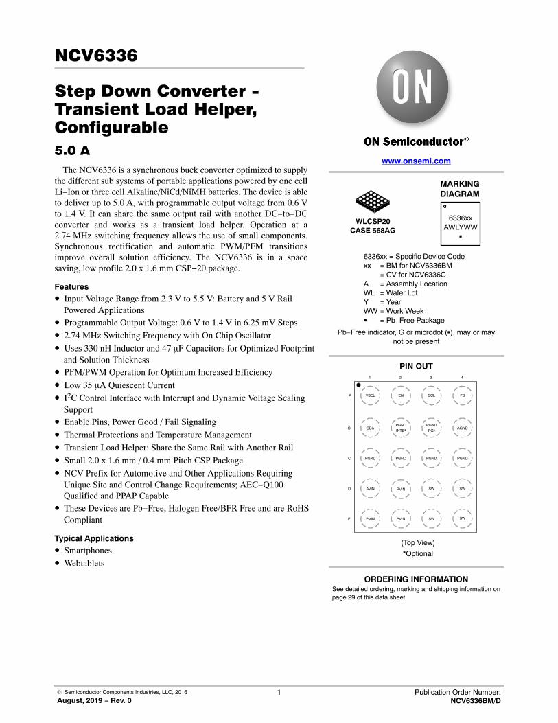
WLCSP20CASE 568AG
MARKINGDIAGRAM
www.onsemi.com
See detailed ordering, marking and shipping information onpage 29 of this data sheet.
ORDERING INFORMATION
6336xx = Specific Device Codexx = BM for NCV6336BM
= CV for NCV6336CA = Assembly LocationWL = Wafer LotY = YearWW = Work Week� = Pb−Free Package
Pb−Free indicator, G or microdot (�), may or maynot be present
4
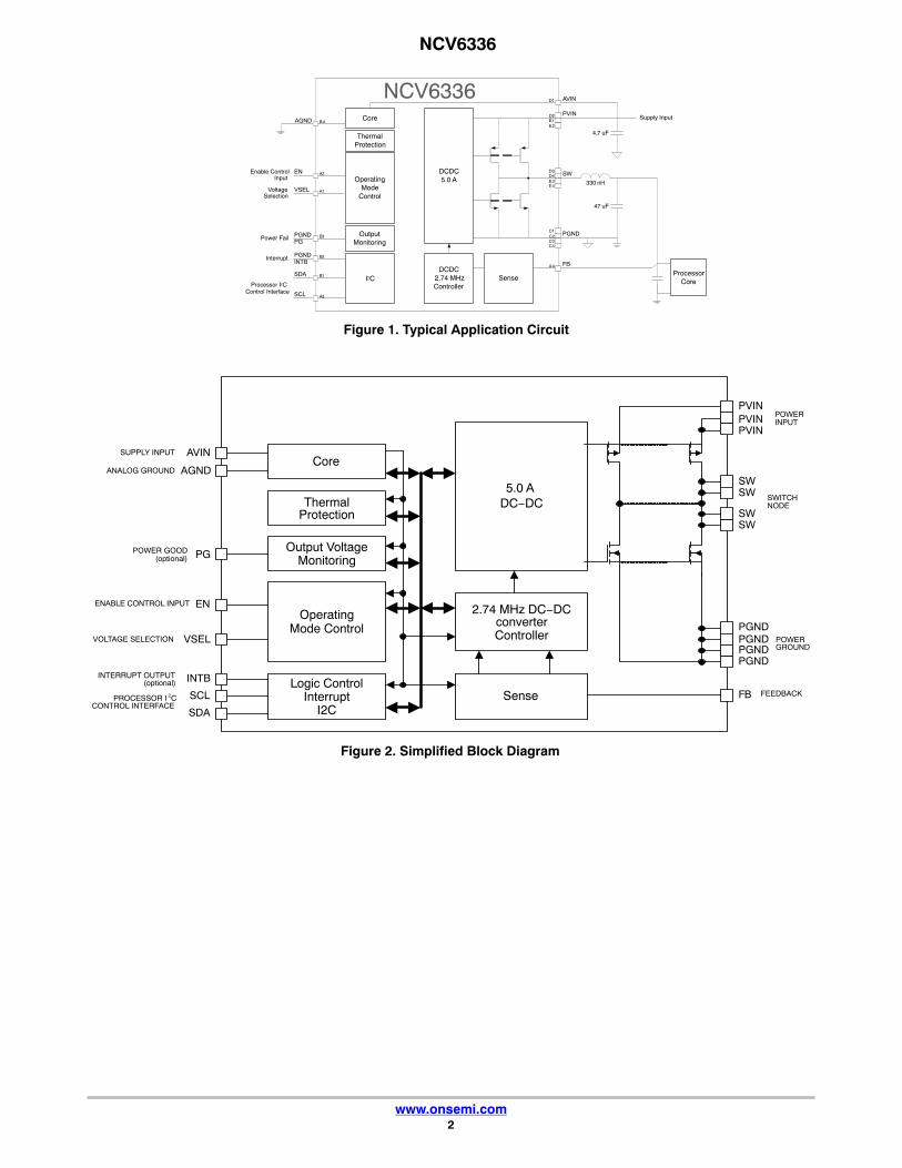
PVIN
AVIN
SW
SW
PVIN
PGND
PGND
INTB*
SCLEN
PVIN
PGNDPGND
SDAPGND
PG*
VSEL
SW
SW
PGND
FB
AGND
321
E
D
C
B
A
PIN OUT
(Top View)
*Optional
6336xxAWLYWW
�
NCV6336
www.onsemi.com2
330 nH
47 uF
ProcessorCore
NCV6336
I�C
ThermalProtection
Processor I�CControl Interface
OperatingMode
Control
OutputMonitoring
VoltageSelection
Interrupt
Power Fail
DCDC5.0 A
Supply Input
DCDC2.74 MHzController
Sense
Enable ControlInput
4.7 uF
SDA
SCL
AGND
PGNDINTB
PGNDPG
VSEL
EN
Core
SW
PVIN
PGND
FB
D2E1B4
A2
A1
B3
B2
B1
A3
D3D4E3E4
C1C2C3C4
A4
E2
D1 AVIN
Figure 1. Typical Application Circuit
Figure 2. Simplified Block Diagram
Core
ThermalProtection
Output VoltageMonitoring
OperatingMode Control
Logic ControlInterrupt
I2C
2.74 MHz DC−DCconverterController
Sense
EN
AGND
PG
VSEL
INTB
SCL
SDA
SWSW
SWSW
PGND
PGNDPGNDPGND
FB
PVINPVINPVIN
5.0 ADC−DC
ANALOG GROUND
ENABLE CONTROL INPUT
VOLTAGE SELECTION
INTERRUPT OUTPUT(optional)
PROCESSOR I 2CCONTROL INTERFACE
POWER GOOD(optional)
POWER
SWITCH
POWER
FEEDBACK
AVINSUPPLY INPUT
INPUT
NODE
GROUND
NCV6336
www.onsemi.com3
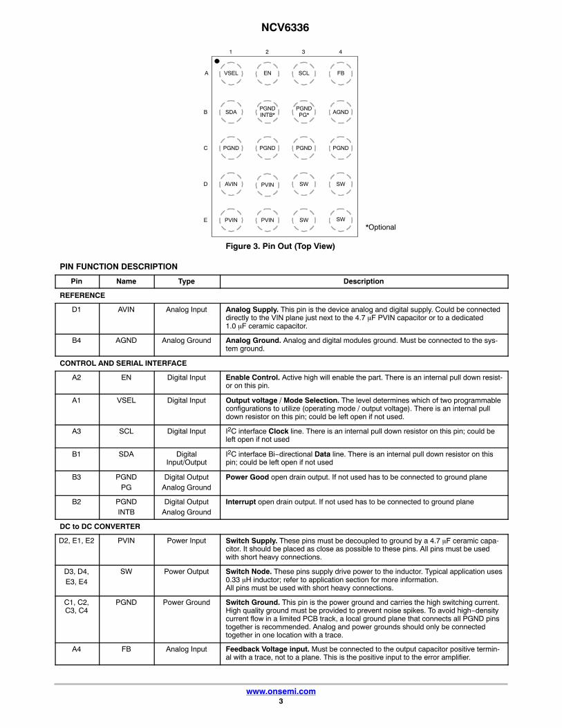
4
PVIN
AVIN
SW
SW
PVIN
PGND
PGNDINTB*
SCLEN
PVIN
PGNDPGND
SDAPGNDPG*
VSEL
SW
SW
PGND
FB
AGND
321
E
D
C
B
A
Figure 3. Pin Out (Top View)
*Optional
PIN FUNCTION DESCRIPTION
Pin Name Type Description
REFERENCE
D1 AVIN Analog Input Analog Supply. This pin is the device analog and digital supply. Could be connecteddirectly to the VIN plane just next to the 4.7 �F PVIN capacitor or to a dedicated1.0 �F ceramic capacitor.
B4 AGND Analog Ground Analog Ground. Analog and digital modules ground. Must be connected to the sys-tem ground.
CONTROL AND SERIAL INTERFACE
A2 EN Digital Input Enable Control. Active high will enable the part. There is an internal pull down resist-or on this pin.
A1 VSEL Digital Input Output voltage / Mode Selection. The level determines which of two programmableconfigurations to utilize (operating mode / output voltage). There is an internal pulldown resistor on this pin; could be left open if not used.
A3 SCL Digital Input I2C interface Clock line. There is an internal pull down resistor on this pin; could beleft open if not used
B1 SDA DigitalInput/Output
I2C interface Bi−directional Data line. There is an internal pull down resistor on thispin; could be left open if not used
B3 PGNDPG
Digital OutputAnalog Ground
Power Good open drain output. If not used has to be connected to ground plane
B2 PGNDINTB
Digital OutputAnalog Ground
Interrupt open drain output. If not used has to be connected to ground plane
DC to DC CONVERTER
D2, E1, E2 PVIN Power Input Switch Supply. These pins must be decoupled to ground by a 4.7 �F ceramic capa-citor. It should be placed as close as possible to these pins. All pins must be usedwith short heavy connections.
D3, D4,E3, E4
SW Power Output Switch Node. These pins supply drive power to the inductor. Typical application uses0.33 �H inductor; refer to application section for more information.All pins must be used with short heavy connections.
C1, C2,C3, C4
PGND Power Ground Switch Ground. This pin is the power ground and carries the high switching current.High quality ground must be provided to prevent noise spikes. To avoid high−densitycurrent flow in a limited PCB track, a local ground plane that connects all PGND pinstogether is recommended. Analog and power grounds should only be connectedtogether in one location with a trace.
A4 FB Analog Input Feedback Voltage input. Must be connected to the output capacitor positive termin-al with a trace, not to a plane. This is the positive input to the error amplifier.
NCV6336
www.onsemi.com4
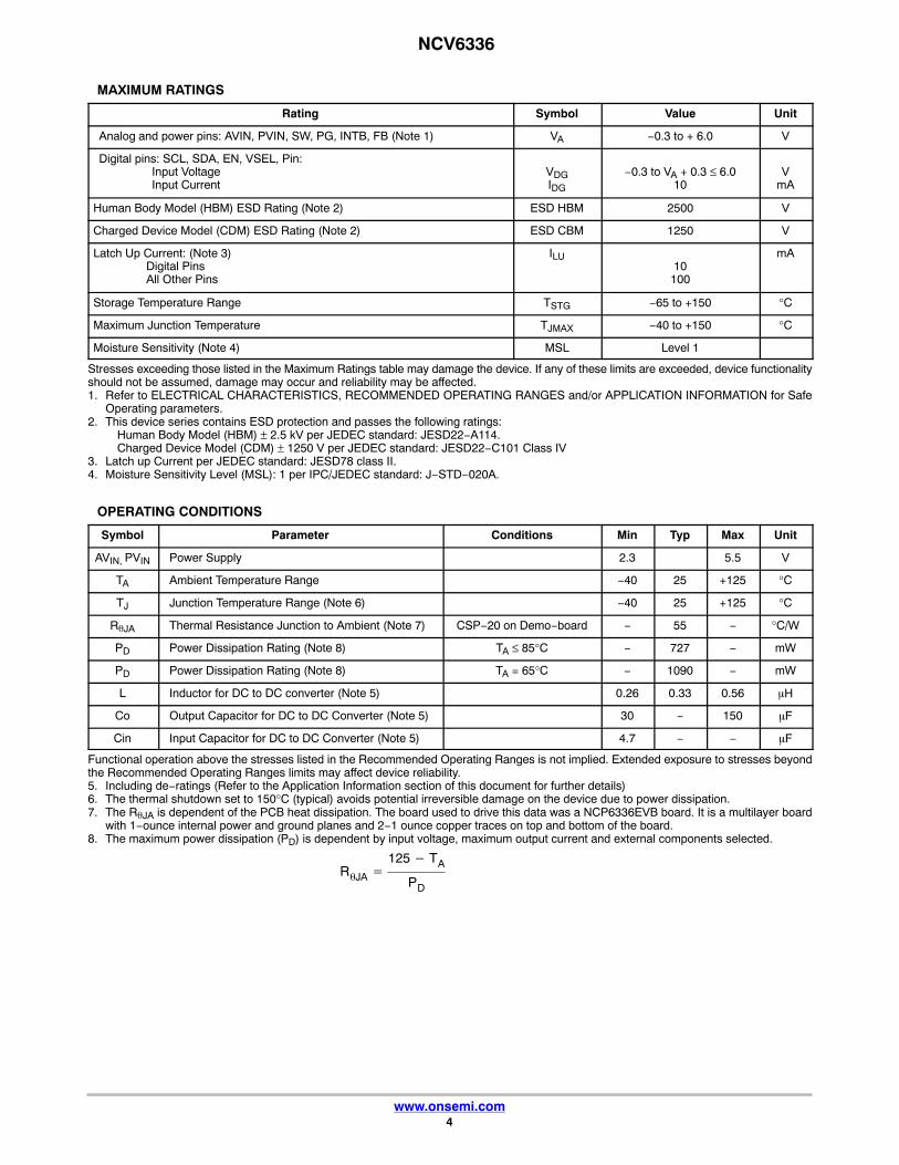
MAXIMUM RATINGS
Rating Symbol Value Unit
Analog and power pins: AVIN, PVIN, SW, PG, INTB, FB (Note 1) VA −0.3 to + 6.0 V
Digital pins: SCL, SDA, EN, VSEL, Pin:Input VoltageInput Current
VDGIDG
−0.3 to VA + 0.3 ≤ 6.010
VmA
Human Body Model (HBM) ESD Rating (Note 2) ESD HBM 2500 V
Charged Device Model (CDM) ESD Rating (Note 2) ESD CBM 1250 V
Latch Up Current: (Note 3)Digital PinsAll Other Pins
ILU10100
mA
Storage Temperature Range TSTG −65 to +150 °C
Maximum Junction Temperature TJMAX −40 to +150 °C
Moisture Sensitivity (Note 4) MSL Level 1
Stresses exceeding those listed in the Maximum Ratings table may damage the device. If any of these limits are exceeded, device functionalityshould not be assumed, damage may occur and reliability may be affected.1. Refer to ELECTRICAL CHARACTERISTICS, RECOMMENDED OPERATING RANGES and/or APPLICATION INFORMATION for Safe
Operating parameters.2. This device series contains ESD protection and passes the following ratings:
Human Body Model (HBM) ± 2.5 kV per JEDEC standard: JESD22−A114.Charged Device Model (CDM) ± 1250 V per JEDEC standard: JESD22−C101 Class IV
3. Latch up Current per JEDEC standard: JESD78 class II.4. Moisture Sensitivity Level (MSL): 1 per IPC/JEDEC standard: J−STD−020A.
OPERATING CONDITIONS
Symbol Parameter Conditions Min Typ Max Unit
AVIN, PVIN Power Supply 2.3 5.5 V
TA Ambient Temperature Range −40 25 +125 °C
TJ Junction Temperature Range (Note 6) −40 25 +125 °C
R�JA Thermal Resistance Junction to Ambient (Note 7) CSP−20 on Demo−board − 55 − °C/W
PD Power Dissipation Rating (Note 8) TA ≤ 85°C − 727 − mW
PD Power Dissipation Rating (Note 8) TA = 65°C − 1090 − mW
L Inductor for DC to DC converter (Note 5) 0.26 0.33 0.56 �H
Co Output Capacitor for DC to DC Converter (Note 5) 30 − 150 �F
Cin Input Capacitor for DC to DC Converter (Note 5) 4.7 − − �F
Functional operation above the stresses listed in the Recommended Operating Ranges is not implied. Extended exposure to stresses beyondthe Recommended Operating Ranges limits may affect device reliability.5. Including de−ratings (Refer to the Application Information section of this document for further details)6. The thermal shutdown set to 150°C (typical) avoids potential irreversible damage on the device due to power dissipation.7. The R�JA is dependent of the PCB heat dissipation. The board used to drive this data was a NCP6336EVB board. It is a multilayer board
with 1−ounce internal power and ground planes and 2−1 ounce copper traces on top and bottom of the board.8. The maximum power dissipation (PD) is dependent by input voltage, maximum output current and external components selected.
R�JA �125 � TA
PD
NCV6336
www.onsemi.com5
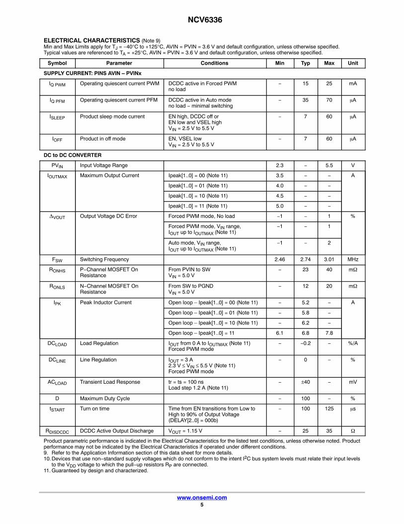
ELECTRICAL CHARACTERISTICS (Note 9)Min and Max Limits apply for TJ = −40°C to +125°C, AVIN = PVIN = 3.6 V and default configuration, unless otherwise specified.Typical values are referenced to TA = +25°C, AVIN = PVIN = 3.6 V and default configuration, unless otherwise specified.
Symbol Parameter Conditions Min Typ Max Unit
SUPPLY CURRENT: PINS AVIN – PVINx
IQ PWM Operating quiescent current PWM DCDC active in Forced PWMno load
− 15 25 mA
IQ PFM Operating quiescent current PFM DCDC active in Auto modeno load − minimal switching
− 35 70 �A
ISLEEP Product sleep mode current EN high, DCDC off orEN low and VSEL highVIN = 2.5 V to 5.5 V
− 7 60 �A
IOFF Product in off mode EN, VSEL lowVIN = 2.5 V to 5.5 V
− 7 60 �A
DC to DC CONVERTER
PVIN Input Voltage Range 2.3 − 5.5 V
IOUTMAX Maximum Output Current Ipeak[1..0] = 00 (Note 11) 3.5 − − A
Ipeak[1..0] = 01 (Note 11) 4.0 − −
Ipeak[1..0] = 10 (Note 11) 4.5 − −
Ipeak[1..0] = 11 (Note 11) 5.0 − −
�VOUT Output Voltage DC Error Forced PWM mode, No load −1 − 1 %
Forced PWM mode, VIN range,IOUT up to IOUTMAX (Note 11)
−1 − 1
Auto mode, VIN range,IOUT up to IOUTMAX (Note 11)
−1 − 2
FSW Switching Frequency 2.46 2.74 3.01 MHz
RONHS P−Channel MOSFET OnResistance
From PVIN to SWVIN = 5.0 V
− 23 40 m�
RONLS N−Channel MOSFET OnResistance
From SW to PGND VIN = 5.0 V
− 12 20 m�
IPK Peak Inductor Current Open loop – Ipeak[1..0] = 00 (Note 11) − 5.2 − A
Open loop – Ipeak[1..0] = 01 (Note 11) − 5.8 −
Open loop – Ipeak[1..0] = 10 (Note 11) − 6.2 −
Open loop – Ipeak[1..0] = 11 6.1 6.8 7.8
DCLOAD Load Regulation IOUT from 0 A to IOUTMAX (Note 11)Forced PWM mode
− −0.2 − %/A
DCLINE Line Regulation IOUT = 3 A2.3 V ≤ VIN ≤ 5.5 V (Note 11)Forced PWM mode
− 0 − %
ACLOAD Transient Load Response tr = ts = 100 nsLoad step 1.2 A (Note 11)
− ±40 − mV
D Maximum Duty Cycle − 100 − %
tSTART Turn on time Time from EN transitions from Low toHigh to 90% of Output Voltage(DELAY[2..0] = 000b)
− 100 125 �s
RDISDCDC DCDC Active Output Discharge VOUT = 1.15 V − 25 35 �
Product parametric performance is indicated in the Electrical Characteristics for the listed test conditions, unless otherwise noted. Productperformance may not be indicated by the Electrical Characteristics if operated under different conditions.9. Refer to the Application Information section of this data sheet for more details.10.Devices that use non−standard supply voltages which do not conform to the intent I2C bus system levels must relate their input levels
to the VDD voltage to which the pull−up resistors RP are connected.11. Guaranteed by design and characterized.
NCV6336
www.onsemi.com6
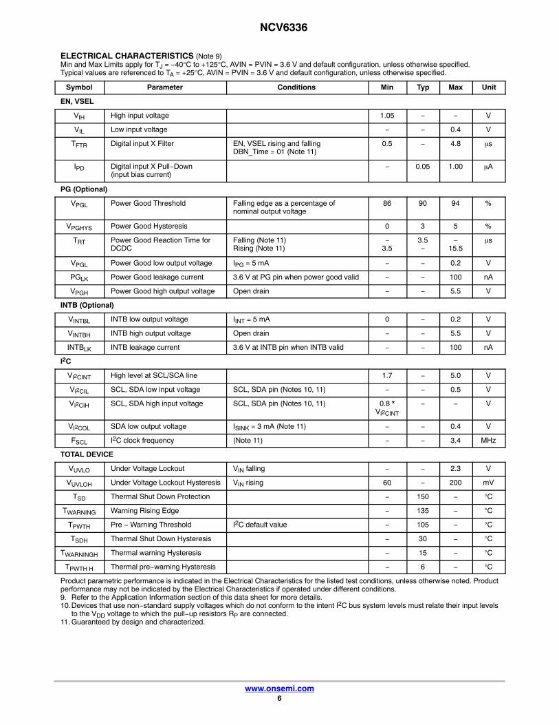
ELECTRICAL CHARACTERISTICS (Note 9)Min and Max Limits apply for TJ = −40°C to +125°C, AVIN = PVIN = 3.6 V and default configuration, unless otherwise specified.Typical values are referenced to TA = +25°C, AVIN = PVIN = 3.6 V and default configuration, unless otherwise specified.
Symbol UnitMaxTypMinConditionsParameter
EN, VSEL
VIH High input voltage 1.05 − − V
VIL Low input voltage − − 0.4 V
TFTR Digital input X Filter EN, VSEL rising and fallingDBN_Time = 01 (Note 11)
0.5 − 4.8 �s
IPD Digital input X Pull−Down(input bias current)
− 0.05 1.00 �A
PG (Optional)
VPGL Power Good Threshold Falling edge as a percentage ofnominal output voltage
86 90 94 %
VPGHYS Power Good Hysteresis 0 3 5 %
TRT Power Good Reaction Time forDCDC
Falling (Note 11)Rising (Note 11)
−3.5
3.5−
−15.5
�s
VPGL Power Good low output voltage IPG = 5 mA − − 0.2 V
PGLK Power Good leakage current 3.6 V at PG pin when power good valid − − 100 nA
VPGH Power Good high output voltage Open drain − − 5.5 V
INTB (Optional)
VINTBL INTB low output voltage IINT = 5 mA 0 − 0.2 V
VINTBH INTB high output voltage Open drain − − 5.5 V
INTBLK INTB leakage current 3.6 V at INTB pin when INTB valid − − 100 nA
I2C
VI2CINT High level at SCL/SCA line 1.7 − 5.0 V
VI2CIL SCL, SDA low input voltage SCL, SDA pin (Notes 10, 11) − − 0.5 V
VI2CIH SCL, SDA high input voltage SCL, SDA pin (Notes 10, 11) 0.8 *VI2CINT
− − V
VI2COL SDA low output voltage ISINK = 3 mA (Note 11) − − 0.4 V
FSCL I2C clock frequency (Note 11) − − 3.4 MHz
TOTAL DEVICE
VUVLO Under Voltage Lockout VIN falling − − 2.3 V
VUVLOH Under Voltage Lockout Hysteresis VIN rising 60 − 200 mV
TSD Thermal Shut Down Protection − 150 − °C
TWARNING Warning Rising Edge − 135 − °C
TPWTH Pre − Warning Threshold I2C default value − 105 − °C
TSDH Thermal Shut Down Hysteresis − 30 − °C
TWARNINGH Thermal warning Hysteresis − 15 − °C
TPWTH H Thermal pre−warning Hysteresis − 6 − °C
Product parametric performance is indicated in the Electrical Characteristics for the listed test conditions, unless otherwise noted. Productperformance may not be indicated by the Electrical Characteristics if operated under different conditions.9. Refer to the Application Information section of this data sheet for more details.10.Devices that use non−standard supply voltages which do not conform to the intent I2C bus system levels must relate their input levels
to the VDD voltage to which the pull−up resistors RP are connected.11. Guaranteed by design and characterized.
NCV6336
www.onsemi.com7
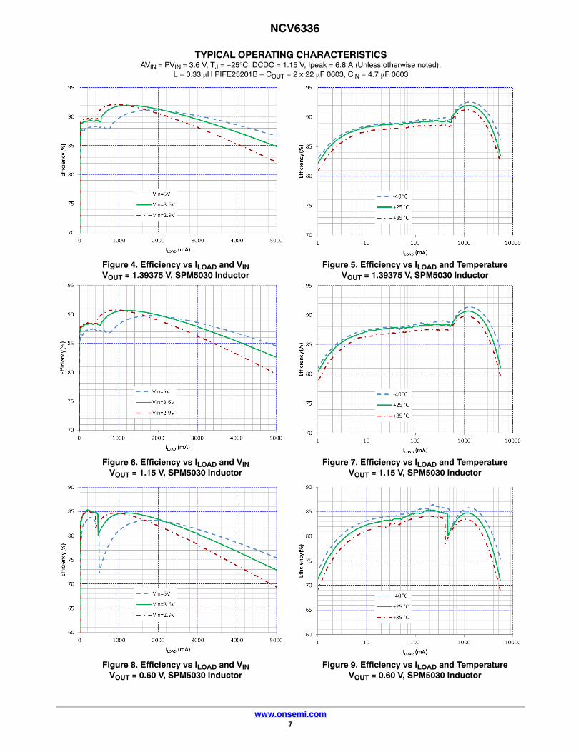
TYPICAL OPERATING CHARACTERISTICSAVIN = PVIN = 3.6 V, TJ = +25°C, DCDC = 1.15 V, Ipeak = 6.8 A (Unless otherwise noted).
L = 0.33 �H PIFE25201B – COUT = 2 x 22 �F 0603, CIN = 4.7 �F 0603
Figure 4. Efficiency vs ILOAD and VINVOUT = 1.39375 V, SPM5030 Inductor
Figure 5. Efficiency vs ILOAD and TemperatureVOUT = 1.39375 V, SPM5030 Inductor
Figure 6. Efficiency vs ILOAD and VINVOUT = 1.15 V, SPM5030 Inductor
Figure 7. Efficiency vs ILOAD and TemperatureVOUT = 1.15 V, SPM5030 Inductor
Figure 8. Efficiency vs ILOAD and VINVOUT = 0.60 V, SPM5030 Inductor
Figure 9. Efficiency vs ILOAD and TemperatureVOUT = 0.60 V, SPM5030 Inductor
NCV6336
www.onsemi.com8
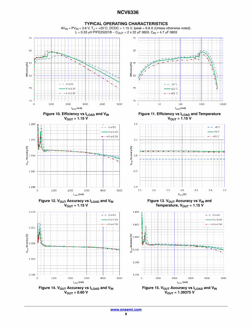
TYPICAL OPERATING CHARACTERISTICSAVIN = PVIN = 3.6 V, TJ = +25°C, DCDC = 1.15 V, Ipeak = 6.8 A (Unless otherwise noted).
L = 0.33 �H PIFE25201B – COUT = 2 x 22 �F 0603, CIN = 4.7 �F 0603
Figure 10. Efficiency vs ILOAD and VINVOUT = 1.15 V
Figure 11. Efficiency vs ILOAD and TemperatureVOUT = 1.15 V
Figure 12. VOUT Accuracy vs ILOAD and VINVOUT = 1.15 V
Figure 13. VOUT Accuracy vs VIN andTemperature, VOUT = 1.15 V
Figure 14. VOUT Accuracy vs ILOAD and VINVOUT = 0.60 V
Figure 15. VOUT Accuracy vs ILOAD and VINVOUT = 1.39375 V
NCV6336
www.onsemi.com9
TYPICAL OPERATING CHARACTERISTICSAVIN = PVIN = 3.6 V, TJ = +25°C, DCDC = 1.15 V, Ipeak = 6.8 A (Unless otherwise noted).
L = 0.33 �H PIFE25201B – COUT = 2 x 22 �F 0603, CIN = 4.7 �F 0603
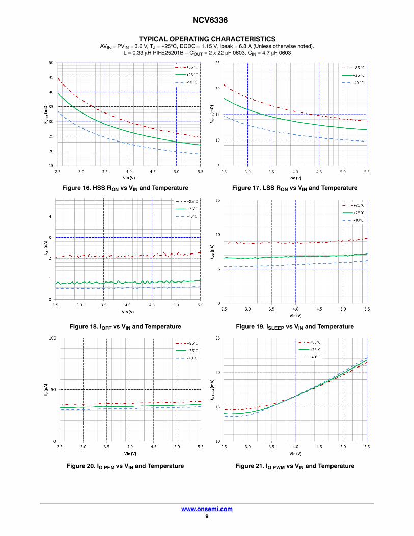
Figure 16. HSS RON vs VIN and Temperature Figure 17. LSS RON vs VIN and Temperature
Figure 18. IOFF vs VIN and Temperature Figure 19. ISLEEP vs VIN and Temperature
Figure 20. IQ PFM vs VIN and Temperature Figure 21. IQ PWM vs VIN and Temperature
NCV6336
www.onsemi.com10
TYPICAL OPERATING CHARACTERISTICSAVIN = PVIN = 3.6 V, TJ = +25°C, DCDC = 1.15 V, Ipeak = 6.8 A (Unless otherwise noted).
L = 0.33 �H PIFE25201B – COUT = 2 x 22 �F 0603, CIN = 4.7 �F 0603
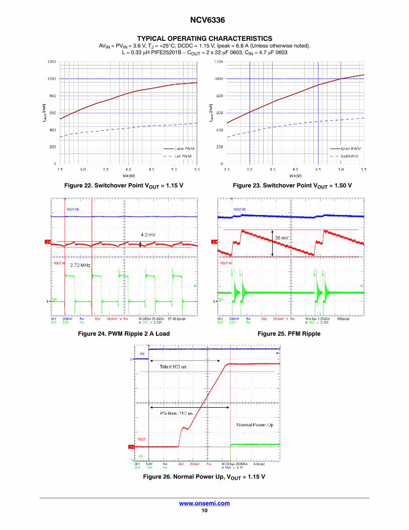
Figure 22. Switchover Point VOUT = 1.15 V Figure 23. Switchover Point VOUT = 1.50 V
Figure 24. PWM Ripple 2 A Load Figure 25. PFM Ripple
Figure 26. Normal Power Up, VOUT = 1.15 V
NCV6336
www.onsemi.com11
TYPICAL OPERATING CHARACTERISTICSAVIN = PVIN = 3.6 V, TJ = +25°C, DCDC = 1.15 V, Ipeak = 6.8 A (Unless otherwise noted).
L = 0.33 �H PIFE25201B – COUT = 2 x 22 �F 0603, CIN = 4.7 �F 0603
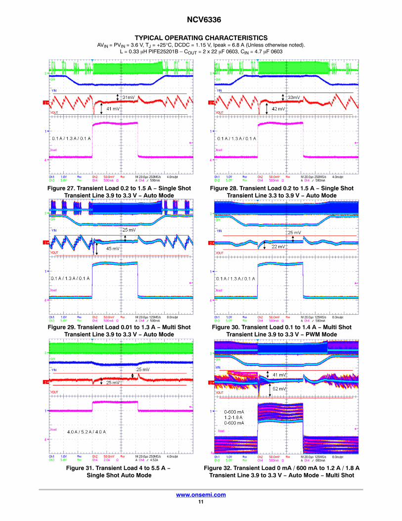
Figure 27. Transient Load 0.2 to 1.5 A − Single ShotTransient Line 3.9 to 3.3 V − Auto Mode
Figure 28. Transient Load 0.2 to 1.5 A − Single ShotTransient Line 3.3 to 3.9 V − Auto Mode
Figure 29. Transient Load 0.01 to 1.3 A − Multi ShotTransient Line 3.9 to 3.3 V − Auto Mode
Figure 30. Transient Load 0.1 to 1.4 A − Multi ShotTransient Line 3.9 to 3.3 V − PWM Mode
Figure 31. Transient Load 4 to 5.5 A − Single Shot Auto Mode
Figure 32. Transient Load 0 mA / 600 mA to 1.2 A / 1.8 ATransient Line 3.9 to 3.3 V − Auto Mode − Multi Shot
NCV6336
www.onsemi.com12
DETAILED OPERATING DESCRIPTION
Detailed DescriptionsThe NCV6336 is voltage mode stand−alone synchronous
DC to DC converter optimized to supply different subsystems of portable applications powered by one cell Li−Ionor three cells Alkaline/NiCd/NiMh. The IC can deliver up to5 A at an I2C selectable voltage ranging from 0.6 V to 1.5 V.It can share the same output rail with another DC to DCconverter and works as a transient load helper withoutsinking current on shared rail. A 2.74 MHz switchingfrequency allows the use of smaller output filtercomponents. Synchronous rectification and automaticPWM/PFM transitions improve overall solution efficiency.Forced PWM is also configurable. Operating modes,configuration, and output power can be easily selected eitherby using digital I/O pins or by programming a set of registersusing an I2C compatible interface capable of operation up to3.4 MHz. Default I2C settings are factory programmable.
DC to DC Converter OperationThe converter is a synchronous rectifier type with both
high side and low side integrated switches. Neither externaltransistor nor diodes are required for NCV6336 operation.Feedback and compensation network are also fullyintegrated. The converter can operate in two differentmodes: PWM and PFM. The transition between PWM/PFMmodes can occur automatically or the switcher can be placedin forced PWM mode by I2C programming (PWMVSEL0/ PWMVSEL1 bits of COMMAND register).
PWM (Pulse Width Modulation) Operating ModeIn medium and high load conditions, NCV6336 operates
in PWM mode from a fixed clock and adapts its duty cycleto regulate the desired output voltage. In this mode, theinductor current is in CCM (Continuous Current Mode) andthe voltage is regulated by PWM. The internal N−MOSFETswitch operates as synchronous rectifier and is drivencomplementary to the P−MOSFET switch. In CCM, thelower switch (N−MOSFET) in a synchronous converterprovides a lower voltage drop than the diode in anasynchronous converter, which provides less loss and higherefficiency.
PFM (Pulse Frequency Modulation) Operating ModeIn order to save power and improve efficiency at low loads
the NCV6336 operates in PFM mode as the inductor currentdrops into DCM (Discontinuous Current Mode). The upperFET on time is kept constant and the switching frequency isvariable. Output voltage is regulated by varying theswitching frequency which becomes proportional to loadingcurrent. As it does in PWM mode, the internal N−MOSFEToperates as synchronous rectifier after each P−MOSFETon−pulse. When load increases and current in inductorbecomes continuous again, the controller automaticallyturns back to PWM mode.
Forced PWMThe NCV6336 can be programmed to only use PWM and
disable the transition to PFM if so desired.
Output StageNCV6336 is a 3.5 A to 5.0 A output current capable
integrated DC to DC converter. To supply such a highcurrent, the internal MOSFETs need to be large.
Inductor Peak Current LimitationDuring normal operation, peak current limitation will
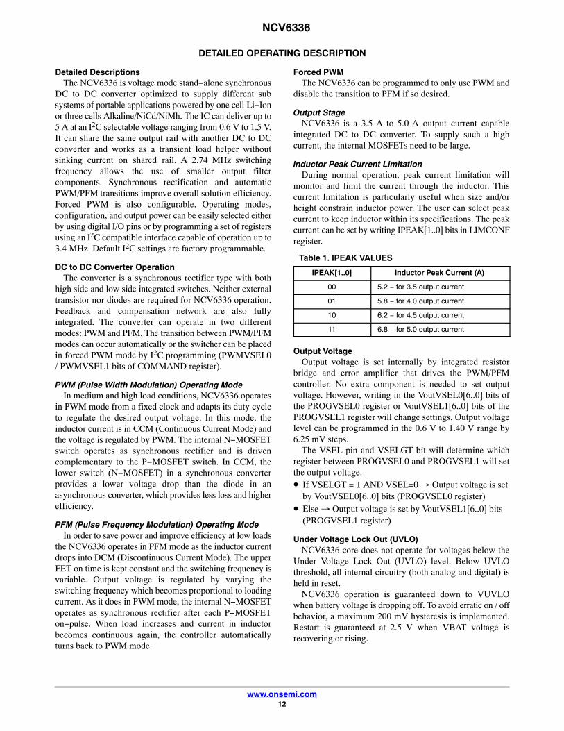
monitor and limit the current through the inductor. Thiscurrent limitation is particularly useful when size and/orheight constrain inductor power. The user can select peakcurrent to keep inductor within its specifications. The peakcurrent can be set by writing IPEAK[1..0] bits in LIMCONFregister.
Table 1. IPEAK VALUES
IPEAK[1..0] Inductor Peak Current (A)
00 5.2 − for 3.5 output current
01 5.8 − for 4.0 output current
10 6.2 − for 4.5 output current
11 6.8 − for 5.0 output current
Output VoltageOutput voltage is set internally by integrated resistor
bridge and error amplifier that drives the PWM/PFMcontroller. No extra component is needed to set outputvoltage. However, writing in the VoutVSEL0[6..0] bits ofthe PROGVSEL0 register or VoutVSEL1[6..0] bits of thePROGVSEL1 register will change settings. Output voltagelevel can be programmed in the 0.6 V to 1.40 V range by6.25 mV steps.
The VSEL pin and VSELGT bit will determine whichregister between PROGVSEL0 and PROGVSEL1 will setthe output voltage.• If VSELGT = 1 AND VSEL=0 � Output voltage is set
by VoutVSEL0[6..0] bits (PROGVSEL0 register)• Else � Output voltage is set by VoutVSEL1[6..0] bits
(PROGVSEL1 register)
Under Voltage Lock Out (UVLO)NCV6336 core does not operate for voltages below the
Under Voltage Lock Out (UVLO) level. Below UVLOthreshold, all internal circuitry (both analog and digital) isheld in reset.
NCV6336 operation is guaranteed down to VUVLOwhen battery voltage is dropping off. To avoid erratic on / offbehavior, a maximum 200 mV hysteresis is implemented.Restart is guaranteed at 2.5 V when VBAT voltage isrecovering or rising.
NCV6336
www.onsemi.com13
Thermal Management
Thermal Shut Down (TSD)The thermal capability of IC can be exceeded due to step
down converter output stage power level. A thermalprotection circuitry is therefore implemented to prevent theIC from damage. This protection circuitry is only activatedwhen the core is in active mode (output voltage is turned on).During thermal shut down, output voltage is turned off.
When NCV6336 returns from thermal shutdown, it canre−start in 2 different configurations depending on REARMbit in the LIMCONF register (see register descriptionsection):• If REARM = 0 then NCV6336 does not re−start after
TSD. To restart, an EN pin toggle is required.• If REARM = 1, NCV6336 re−starts with register values
set prior to thermal shutdown.A Thermal shut down interrupt is raised upon this event.Thermal shut down threshold is set at 150°C (typical)
when the die temperature increases and, in order to avoiderratic on / off behavior, a 30°C hysteresis is implemented.After a typical 150°C thermal shut down, NCV6336 willresume to normal operation when the die temperature coolsto 120°C.
Thermal WarningsIn addition to the TSD, the die temperature monitoring
will flag potential die over temperature. A thermal warningand thermal pre−warning sensor and interrupts areimplemented. These can inform the processor thatNCV6336 is closed to its thermal shutdown, so preventivemeasures to cool down die temperature can be taken bysoftware.
The Warning threshold is set by hardware to 135°C typicalwhen the die temperature increases. The Pre−Warningthreshold is set by default to 105°C, but can be changed byuser by setting the TPWTH[1..0] bits in the LIMCONFregister.
Active Output DischargeTo make sure that no residual voltage remains in the power
supply rail when disabled, an active discharge path canground the NCV6336 output voltage.
For maximum flexibility, this feature can be easilydisabled or enabled with DISCHG bit in PGOOD register.By default the discharge path is enabled.
However the discharged path is activated during the first100 �s after battery insertion.
EnablingThe EN pin controls NCV6336 start up. EN pin Low to
High transition starts the power up sequencer. If EN is madelow, the DC to DC converter is turned off and device enters:• In Sleep Mode if Sleep_Mode I2C bit is high or VSEL
is high,• In Off Mode if Sleep_Mode I2C bit and VSEL are low.
When EN pin is set to a high level, the DC to DC convertercan be enabled / disabled by writing the ENVSEL0 orENVSEL1 bit of the PROGVSEL0 and PROGVSEL1registers: If ENx I2C bit is high, DC to DC converter isactivated, If ENx I2C is low the DC to DC converter is turnedoff and device enters in Sleep Mode
A built in pull down resistor disables the device when thispin is left unconnected or not driven. EN pin activity doesnot generate any digital reset.
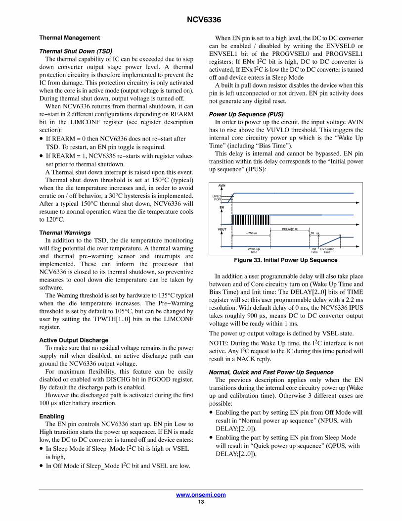
Power Up Sequence (PUS)In order to power up the circuit, the input voltage AVIN
has to rise above the VUVLO threshold. This triggers theinternal core circuitry power up which is the “Wake UpTime” (including “Bias Time”).
This delay is internal and cannot be bypassed. EN pintransition within this delay corresponds to the “Initial powerup sequence” (IPUS):
PORUVLO
AVIN
EN
Wake upTime
DELAY[2..0]~ 750 us 35 us
VOUT
DVS rampTime
InitTime
ÏÏÏÏÏÏÏÏÏÏ
Figure 33. Initial Power Up Sequence
In addition a user programmable delay will also take placebetween end of Core circuitry turn on (Wake Up Time andBias Time) and Init time: The DELAY[2..0] bits of TIMEregister will set this user programmable delay with a 2.2 msresolution. With default delay of 0 ms, the NCV6336 IPUStakes roughly 900 �s, means DC to DC converter outputvoltage will be ready within 1 ms.
The power up output voltage is defined by VSEL state.
NOTE: During the Wake Up time, the I2C interface is notactive. Any I2C request to the IC during this time period willresult in a NACK reply.
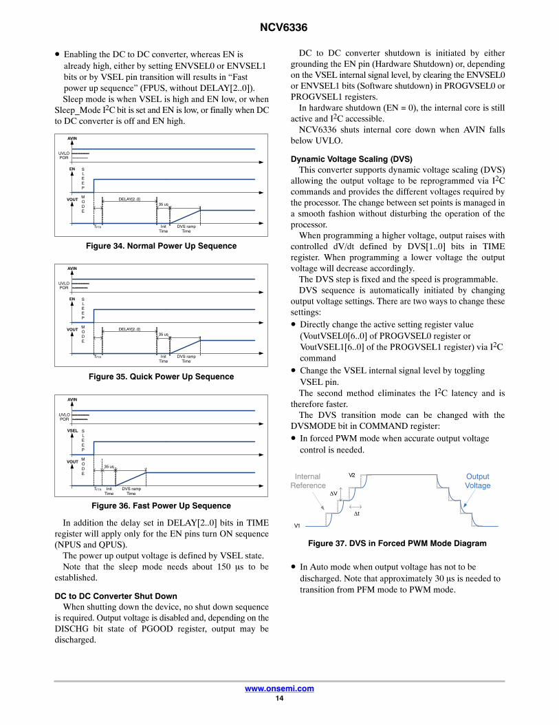
Normal, Quick and Fast Power Up SequenceThe previous description applies only when the EN
transitions during the internal core circuitry power up (Wakeup and calibration time). Otherwise 3 different cases arepossible:• Enabling the part by setting EN pin from Off Mode will
result in “Normal power up sequence” (NPUS, withDELAY;[2..0]).
• Enabling the part by setting EN pin from Sleep Modewill result in “Quick power up sequence” (QPUS, withDELAY;[2..0]).
NCV6336
www.onsemi.com14
• Enabling the DC to DC converter, whereas EN isalready high, either by setting ENVSEL0 or ENVSEL1bits or by VSEL pin transition will results in “Fastpower up sequence” (FPUS, without DELAY[2..0]).Sleep mode is when VSEL is high and EN low, or when
Sleep_Mode I2C bit is set and EN is low, or finally when DCto DC converter is off and EN high.
Figure 34. Normal Power Up Sequence
SLEEP
MODE
PORUVLO
AVIN
EN
DELAY[2..0]35 us
VOUT
DVS rampTime
InitTime
TFTR
SLEEP
MODE
PORUVLO
AVIN
EN
DELAY[2..0]35 us
VOUT
DVS rampTime
InitTime
TFTR
Figure 35. Quick Power Up Sequence
SLEEP
MODE
PORUVLO
AVIN
VSEL
35 usVOUT
DVS rampTime
InitTime
TFTR
Figure 36. Fast Power Up Sequence
In addition the delay set in DELAY[2..0] bits in TIMEregister will apply only for the EN pins turn ON sequence(NPUS and QPUS).
The power up output voltage is defined by VSEL state.Note that the sleep mode needs about 150 �s to be
established.
DC to DC Converter Shut DownWhen shutting down the device, no shut down sequence
is required. Output voltage is disabled and, depending on theDISCHG bit state of PGOOD register, output may bedischarged.
DC to DC converter shutdown is initiated by eithergrounding the EN pin (Hardware Shutdown) or, dependingon the VSEL internal signal level, by clearing the ENVSEL0or ENVSEL1 bits (Software shutdown) in PROGVSEL0 orPROGVSEL1 registers.
In hardware shutdown (EN = 0), the internal core is stillactive and I2C accessible.
NCV6336 shuts internal core down when AVIN fallsbelow UVLO.
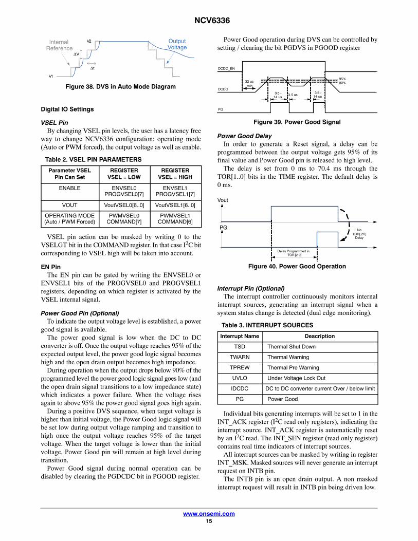
Dynamic Voltage Scaling (DVS)This converter supports dynamic voltage scaling (DVS)
allowing the output voltage to be reprogrammed via I2Ccommands and provides the different voltages required bythe processor. The change between set points is managed ina smooth fashion without disturbing the operation of theprocessor.
When programming a higher voltage, output raises withcontrolled dV/dt defined by DVS[1..0] bits in TIMEregister. When programming a lower voltage the outputvoltage will decrease accordingly.
The DVS step is fixed and the speed is programmable.DVS sequence is automatically initiated by changing
output voltage settings. There are two ways to change thesesettings:• Directly change the active setting register value
(VoutVSEL0[6..0] of PROGVSEL0 register orVoutVSEL1[6..0] of the PROGVSEL1 register) via I2Ccommand
• Change the VSEL internal signal level by togglingVSEL pin.The second method eliminates the I2C latency and is
therefore faster.The DVS transition mode can be changed with the
DVSMODE bit in COMMAND register:• In forced PWM mode when accurate output voltage
control is needed.
V2
V1
InternalReference
OutputVoltage
�t
�V
Figure 37. DVS in Forced PWM Mode Diagram
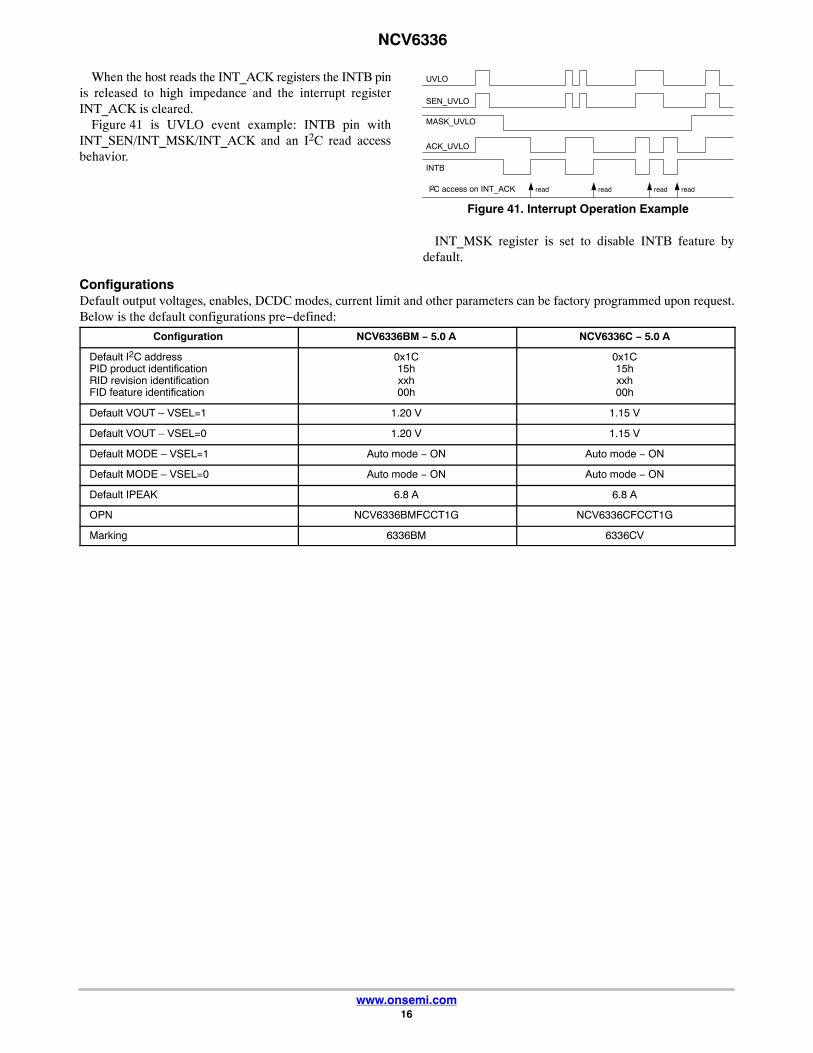
• In Auto mode when output voltage has not to bedischarged. Note that approximately 30 �s is needed totransition from PFM mode to PWM mode.
NCV6336
www.onsemi.com15
V2
V1
InternalReference
OutputVoltage
�t
�V
Figure 38. DVS in Auto Mode Diagram
Digital IO Settings
VSEL PinBy changing VSEL pin levels, the user has a latency free
way to change NCV6336 configuration: operating mode(Auto or PWM forced), the output voltage as well as enable.
Table 2. VSEL PIN PARAMETERS
Parameter VSELPin Can Set
REGISTERVSEL = LOW
REGISTERVSEL = HIGH
ENABLE ENVSEL0PROGVSEL0[7]
ENVSEL1PROGVSEL1[7]
VOUT VoutVSEL0[6..0] VoutVSEL1[6..0]
OPERATING MODE(Auto / PWM Forced)
PWMVSEL0COMMAND[7]
PWMVSEL1COMMAND[6]
VSEL pin action can be masked by writing 0 to theVSELGT bit in the COMMAND register. In that case I2C bitcorresponding to VSEL high will be taken into account.
EN PinThe EN pin can be gated by writing the ENVSEL0 or
ENVSEL1 bits of the PROGVSEL0 and PROGVSEL1registers, depending on which register is activated by theVSEL internal signal.
Power Good Pin (Optional)To indicate the output voltage level is established, a power
good signal is available.The power good signal is low when the DC to DC
converter is off. Once the output voltage reaches 95% of theexpected output level, the power good logic signal becomeshigh and the open drain output becomes high impedance.
During operation when the output drops below 90% of theprogrammed level the power good logic signal goes low (andthe open drain signal transitions to a low impedance state)which indicates a power failure. When the voltage risesagain to above 95% the power good signal goes high again.
During a positive DVS sequence, when target voltage ishigher than initial voltage, the Power Good logic signal willbe set low during output voltage ramping and transition tohigh once the output voltage reaches 95% of the targetvoltage. When the target voltage is lower than the initialvoltage, Power Good pin will remain at high level duringtransition.
Power Good signal during normal operation can bedisabled by clearing the PGDCDC bit in PGOOD register.
Power Good operation during DVS can be controlled bysetting / clearing the bit PGDVS in PGOOD register
DCDC_EN
32 usmin
DCDC
95%90%
3.5−14 us
3.5−14 us3.5 us
PG
Figure 39. Power Good Signal
Power Good DelayIn order to generate a Reset signal, a delay can be
programmed between the output voltage gets 95% of itsfinal value and Power Good pin is released to high level.
The delay is set from 0 ms to 70.4 ms through theTOR[1..0] bits in the TIME register. The default delay is0 ms.
Vout
PG
Delay Programmed inTOR [2:0]
NoTOR[2:0]
Delay
Figure 40. Power Good Operation
Interrupt Pin (Optional)The interrupt controller continuously monitors internal
interrupt sources, generating an interrupt signal when asystem status change is detected (dual edge monitoring).
Table 3. INTERRUPT SOURCES
Interrupt Name Description
TSD Thermal Shut Down
TWARN Thermal Warning
TPREW Thermal Pre Warning
UVLO Under Voltage Lock Out
IDCDC DC to DC converter current Over / below limit
PG Power Good
Individual bits generating interrupts will be set to 1 in theINT_ACK register (I2C read only registers), indicating theinterrupt source. INT_ACK register is automatically resetby an I2C read. The INT_SEN register (read only register)contains real time indicators of interrupt sources.
All interrupt sources can be masked by writing in registerINT_MSK. Masked sources will never generate an interruptrequest on INTB pin.
The INTB pin is an open drain output. A non maskedinterrupt request will result in INTB pin being driven low.
NCV6336
www.onsemi.com16
When the host reads the INT_ACK registers the INTB pinis released to high impedance and the interrupt registerINT_ACK is cleared.
Figure 41 is UVLO event example: INTB pin withINT_SEN/INT_MSK/INT_ACK and an I2C read accessbehavior.
readI2C access on INT_ACK read read read
INTB
ACK_UVLO
MASK_UVLO
SEN_UVLO
UVLO
Figure 41. Interrupt Operation Example
INT_MSK register is set to disable INTB feature bydefault.
ConfigurationsDefault output voltages, enables, DCDC modes, current limit and other parameters can be factory programmed upon request.Below is the default configurations pre−defined:
Configuration NCV6336BM − 5.0 A NCV6336C − 5.0 A
Default I2C addressPID product identificationRID revision identificationFID feature identification
0x1C15hxxh00h
0x1C15hxxh00h
Default VOUT – VSEL=1 1.20 V 1.15 V
Default VOUT – VSEL=0 1.20 V 1.15 V
Default MODE – VSEL=1 Auto mode − ON Auto mode − ON
Default MODE – VSEL=0 Auto mode − ON Auto mode − ON
Default IPEAK 6.8 A 6.8 A
OPN NCV6336BMFCCT1G NCV6336CFCCT1G
Marking 6336BM 6336CV
NCV6336
www.onsemi.com17
I2C Compatible InterfaceNCV6336 can support a subset of I2C protocol Detailed below.
I2C Communication Description
START IC ADDRESS 1
1� READ
ACK DATA 1 ACK DATA n /ACK STOP
START ACKIC ADDRESS 0
0�WRITE
DATA 1 ACK DATA nACK
/ACKSTOP
FROM MCU to NCPxxxx
FROM NCPxxxx to MCU
READ OUT FROM PART
WRITE INSIDE PART
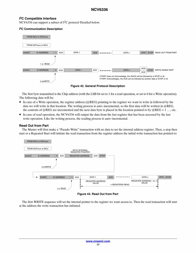
Figure 42. General Protocol Description
If PART does not Acknowledge, the /NACK will be followed by a STOP or Sr.If PART Acknowledges, the ACK can be followed by another data or STOP or Sr
The first byte transmitted is the Chip address (with the LSB bit set to 1 for a read operation, or set to 0 for a Write operation).The following data will be:• In case of a Write operation, the register address (@REG) pointing to the register we want to write in followed by the
data we will write in that location. The writing process is auto−incremental, so the first data will be written in @REG,the contents of @REG are incremented and the next data byte is placed in the location pointed to by @REG + 1 …, etc.
• In case of read operation, the NCV6336 will output the data from the last register that has been accessed by the lastwrite operation. Like the writing process, the reading process is auto−incremental.
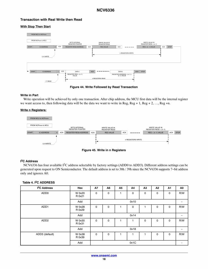
Read Out from PartThe Master will first make a “Pseudo Write” transaction with no data to set the internal address register. Then, a stop then
start or a Repeated Start will initiate the read transaction from the register address the initial write transaction has pointed to:
STOP
IC ADDRESS 1
1� READ
ACKSTART IC ADDRESS 0
0� WRITE
REGISTER ADDRESS ACK
START ACK DATA 1 DATA nACK /ACK STOP
SETS INTERNALREGISTER POINTER
REGISTER ADDRESSVALUE
REGISTER ADDRESS + (n−1)
n REGISTERS READ
FROM MCU to NCPxxxx
FROM NCPxxxx to MCU
Figure 43. Read Out from Part
VALUE
The first WRITE sequence will set the internal pointer to the register we want access to. Then the read transaction will startat the address the write transaction has initiated.
NCV6336
www.onsemi.com18
Transaction with Real Write then Read
With Stop Then Start
REG + (n– 1) VALUE ACK STOP
FROM MCU to NCPxxxx
FROM NCPxxxx to MCU
IC ADDRESS 0
0 � WRITE
ACK REGISTER REG0 ADDRESS ACK REG VALUE ACK
SETS INTERNALREGISTER POINTER
WRITE VALUE INREGISTER REG0
WRITE VALUE INREGISTER REG0 + (n−1)
n REGISTERS WRITE
IC ADDRESS 1
1 � READ
START ACK DATA 1 DATA kACK /ACK STOP
REGISTER REG + (n−1)VALUE
REGISTER ADDRESS + (n−1) +
k REGISTERS READ
START
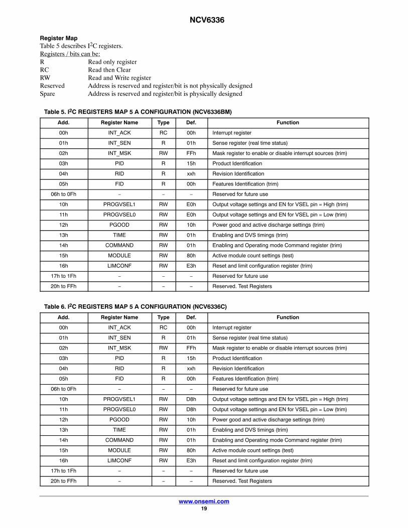
Figure 44. Write Followed by Read Transaction
(k−1) VALUE
Write in PartWrite operation will be achieved by only one transaction. After chip address, the MCU first data will be the internal register
we want access to, then following data will be the data we want to write in Reg, Reg + 1, Reg + 2, …, Reg +n.
Write n Registers:
REG + (n−1) VALUE ACK STOP
FROM MCU to NCPxxxx
FROM NCPxxxx to MCU
START IC ADDRESS 0
0� WRITE
ACK REGISTER REG0 ADDRESS ACK REG VALUE ACK
SETS INTERNALREGISTER POINTER
WRITE VALUE INREGISTER REG0
WRITE VALUE INREGISTER REG0 + (n−1)
n REGISTERS WRITE
Figure 45. Write in n Registers
I2C AddressNCV6336 has four available I2C address selectable by factory settings (ADD0 to ADD3). Different address settings can be
generated upon request to ON Semiconductor. The default address is set to 38h / 39h since the NCV6336 supports 7−bit addressonly and ignores A0.
Table 4. I2C ADDRESS
I2C Address Hex A7 A6 A5 A4 A3 A2 A1 A0
ADD0 W 0x20R 0x21
0 0 1 0 0 0 0 R/W
Add 0x10 −
ADD1 W 0x28R 0x29
0 0 1 0 1 0 0 R/W
Add 0x14 −
ADD2 W 0x30R 0x31
0 0 1 1 0 0 0 R/W
Add 0x18 −
ADD3 (default) W 0x38R 0x39
0 0 1 1 1 0 0 R/W
Add 0x1C −
NCV6336
www.onsemi.com19
Register MapTable 5 describes I2C registers.Registers / bits can be:R Read only registerRC Read then ClearRW Read and Write registerReserved Address is reserved and register/bit is not physically designedSpare Address is reserved and register/bit is physically designed
Table 5. I2C REGISTERS MAP 5 A CONFIGURATION (NCV6336BM)
Add. Register Name Type Def. Function
00h INT_ACK RC 00h Interrupt register
01h INT_SEN R 01h Sense register (real time status)
02h INT_MSK RW FFh Mask register to enable or disable interrupt sources (trim)
03h PID R 15h Product Identification
04h RID R xxh Revision Identification
05h FID R 00h Features Identification (trim)
06h to 0Fh − − − Reserved for future use
10h PROGVSEL1 RW E0h Output voltage settings and EN for VSEL pin = High (trim)
11h PROGVSEL0 RW E0h Output voltage settings and EN for VSEL pin = Low (trim)
12h PGOOD RW 10h Power good and active discharge settings (trim)
13h TIME RW 01h Enabling and DVS timings (trim)
14h COMMAND RW 01h Enabling and Operating mode Command register (trim)
15h MODULE RW 80h Active module count settings (test)
16h LIMCONF RW E3h Reset and limit configuration register (trim)
17h to 1Fh − − − Reserved for future use
20h to FFh − − − Reserved. Test Registers
Table 6. I2C REGISTERS MAP 5 A CONFIGURATION (NCV6336C)
Add. Register Name Type Def. Function
00h INT_ACK RC 00h Interrupt register
01h INT_SEN R 01h Sense register (real time status)
02h INT_MSK RW FFh Mask register to enable or disable interrupt sources (trim)
03h PID R 15h Product Identification
04h RID R xxh Revision Identification
05h FID R 00h Features Identification (trim)
06h to 0Fh − − − Reserved for future use
10h PROGVSEL1 RW D8h Output voltage settings and EN for VSEL pin = High (trim)
11h PROGVSEL0 RW D8h Output voltage settings and EN for VSEL pin = Low (trim)
12h PGOOD RW 10h Power good and active discharge settings (trim)
13h TIME RW 01h Enabling and DVS timings (trim)
14h COMMAND RW 01h Enabling and Operating mode Command register (trim)
15h MODULE RW 80h Active module count settings (test)
16h LIMCONF RW E3h Reset and limit configuration register (trim)
17h to 1Fh − − − Reserved for future use
20h to FFh − − − Reserved. Test Registers
NCV6336
www.onsemi.com20
Registers Description
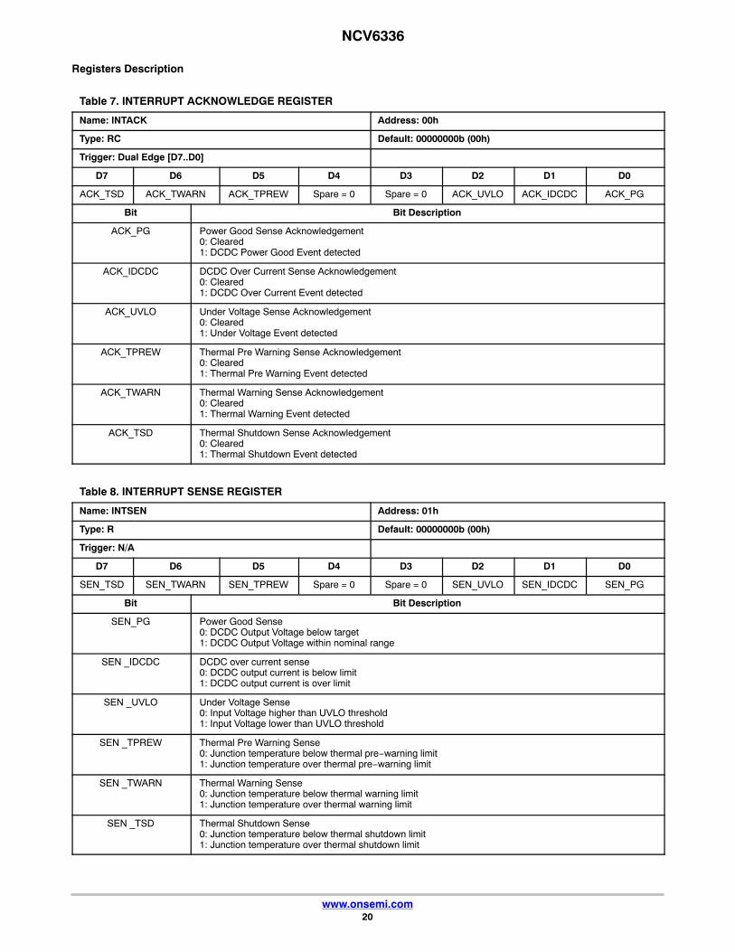
Table 7. INTERRUPT ACKNOWLEDGE REGISTER
Name: INTACK Address: 00h
Type: RC Default: 00000000b (00h)
Trigger: Dual Edge [D7..D0]
D7 D6 D5 D4 D3 D2 D1 D0
ACK_TSD ACK_TWARN ACK_TPREW Spare = 0 Spare = 0 ACK_UVLO ACK_IDCDC ACK_PG
Bit Bit Description
ACK_PG Power Good Sense Acknowledgement0: Cleared1: DCDC Power Good Event detected
ACK_IDCDC DCDC Over Current Sense Acknowledgement0: Cleared1: DCDC Over Current Event detected
ACK_UVLO Under Voltage Sense Acknowledgement0: Cleared1: Under Voltage Event detected
ACK_TPREW Thermal Pre Warning Sense Acknowledgement0: Cleared1: Thermal Pre Warning Event detected
ACK_TWARN Thermal Warning Sense Acknowledgement 0: Cleared1: Thermal Warning Event detected
ACK_TSD Thermal Shutdown Sense Acknowledgement 0: Cleared1: Thermal Shutdown Event detected
Table 8. INTERRUPT SENSE REGISTER
Name: INTSEN Address: 01h
Type: R Default: 00000000b (00h)
Trigger: N/A
D7 D6 D5 D4 D3 D2 D1 D0
SEN_TSD SEN_TWARN SEN_TPREW Spare = 0 Spare = 0 SEN_UVLO SEN_IDCDC SEN_PG
Bit Bit Description
SEN_PG Power Good Sense0: DCDC Output Voltage below target1: DCDC Output Voltage within nominal range
SEN _IDCDC DCDC over current sense0: DCDC output current is below limit1: DCDC output current is over limit
SEN _UVLO Under Voltage Sense0: Input Voltage higher than UVLO threshold1: Input Voltage lower than UVLO threshold
SEN _TPREW Thermal Pre Warning Sense0: Junction temperature below thermal pre−warning limit1: Junction temperature over thermal pre−warning limit
SEN _TWARN Thermal Warning Sense0: Junction temperature below thermal warning limit1: Junction temperature over thermal warning limit
SEN _TSD Thermal Shutdown Sense 0: Junction temperature below thermal shutdown limit1: Junction temperature over thermal shutdown limit
NCV6336
www.onsemi.com21
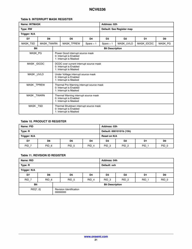
Table 9. INTERRUPT MASK REGISTER
Name: INTMASK Address: 02h
Type: RW Default: See Register map
Trigger: N/A
D7 D6 D5 D4 D3 D2 D1 D0
MASK_TSD MASK_TWARN MASK_TPREW Spare = 1 Spare = 1 MASK_UVLO MASK_IDCDC MASK_PG
Bit Bit Description
MASK_PG Power Good interrupt source mask0: Interrupt is Enabled1: Interrupt is Masked
MASK _IDCDC DCDC over current interrupt source mask0: Interrupt is Enabled1: Interrupt is Masked
MASK _UVLO Under Voltage interrupt source mask0: Interrupt is Enabled1: Interrupt is Masked
MASK _TPREW Thermal Pre Warning interrupt source mask0: Interrupt is Enabled1: Interrupt is Masked
MASK _TWARN Thermal Warning interrupt source mask0: Interrupt is Enabled1: Interrupt is Masked
MASK _TSD Thermal Shutdown interrupt source mask0: Interrupt is Enabled1: Interrupt is Masked
Table 10. PRODUCT ID REGISTER
Name: PID Address: 03h
Type: R Default: 00010101b (15h)
Trigger: N/A Reset on N/A
D7 D6 D5 D4 D3 D2 D1 D0
PID_7 PID_6 PID_5 PID_4 PID_3 PID_2 PID_1 PID_0
Table 11. REVISION ID REGISTER
Name: RID Address: 04h
Type: R Default: xxh
Trigger: N/A
D7 D6 D5 D4 D3 D2 D1 D0
RID_7 RID_6 RID_5 RID_4 RID_3 RID_2 RID_1 RID_0
Bit Bit Description
RID[7..0] Revision Identification00000000
NCV6336
www.onsemi.com22
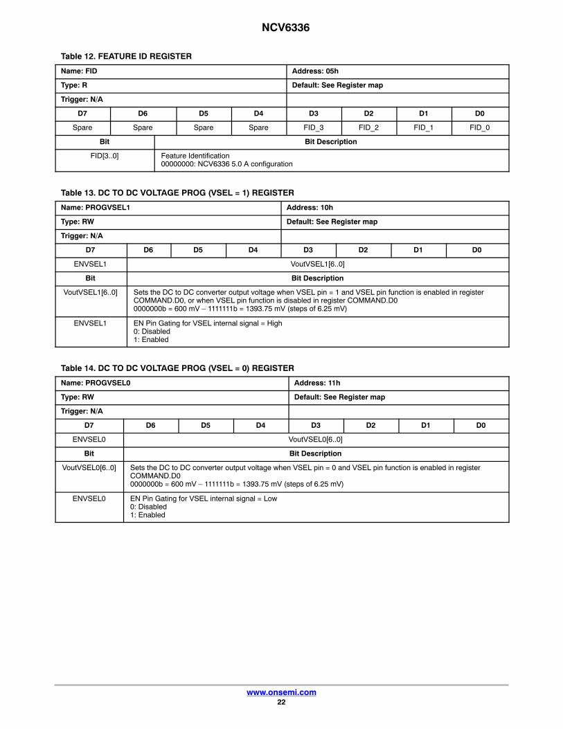
Table 12. FEATURE ID REGISTER
Name: FID Address: 05h
Type: R Default: See Register map
Trigger: N/A
D7 D6 D5 D4 D3 D2 D1 D0
Spare Spare Spare Spare FID_3 FID_2 FID_1 FID_0
Bit Bit Description
FID[3..0] Feature Identification00000000: NCV6336 5.0 A configuration
Table 13. DC TO DC VOLTAGE PROG (VSEL = 1) REGISTER
Name: PROGVSEL1 Address: 10h
Type: RW Default: See Register map
Trigger: N/A
D7 D6 D5 D4 D3 D2 D1 D0
ENVSEL1 VoutVSEL1[6..0]
Bit Bit Description
VoutVSEL1[6..0] Sets the DC to DC converter output voltage when VSEL pin = 1 and VSEL pin function is enabled in registerCOMMAND.D0, or when VSEL pin function is disabled in register COMMAND.D00000000b = 600 mV – 1111111b = 1393.75 mV (steps of 6.25 mV)
ENVSEL1 EN Pin Gating for VSEL internal signal = High0: Disabled1: Enabled
Table 14. DC TO DC VOLTAGE PROG (VSEL = 0) REGISTER
Name: PROGVSEL0 Address: 11h
Type: RW Default: See Register map
Trigger: N/A
D7 D6 D5 D4 D3 D2 D1 D0
ENVSEL0 VoutVSEL0[6..0]
Bit Bit Description
VoutVSEL0[6..0] Sets the DC to DC converter output voltage when VSEL pin = 0 and VSEL pin function is enabled in registerCOMMAND.D00000000b = 600 mV – 1111111b = 1393.75 mV (steps of 6.25 mV)
ENVSEL0 EN Pin Gating for VSEL internal signal = Low0: Disabled1: Enabled
NCV6336
www.onsemi.com23
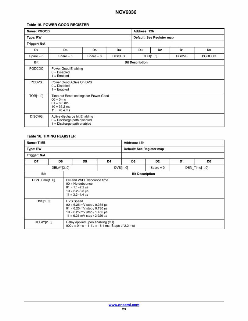
Table 15. POWER GOOD REGISTER
Name: PGOOD Address: 12h
Type: RW Default: See Register map
Trigger: N/A
D7 D6 D5 D4 D3 D2 D1 D0
Spare = 0 Spare = 0 Spare = 0 DISCHG TOR[1..0] PGDVS PGDCDC
Bit Bit Description
PGDCDC Power Good Enabling0 = Disabled1 = Enabled
PGDVS Power Good Active On DVS0 = Disabled1 = Enabled
TOR[1..0] Time out Reset settings for Power Good00 = 0 ms 01 = 8.8 ms 10 = 35.2 ms 11 = 70.4 ms
DISCHG Active discharge bit Enabling0 = Discharge path disabled1 = Discharge path enabled
Table 16. TIMING REGISTER
Name: TIME Address: 13h
Type: RW Default: See Register map
Trigger: N/A
D7 D6 D5 D4 D3 D2 D1 D0
DELAY[2..0] DVS[1..0] Spare = 0 DBN_Time[1..0]
Bit Bit Description
DBN_Time[1..0] EN and VSEL debounce time00 = No debounce01 = 1.1−2.2 �s10 = 2.2−3.3 �s11 = 3.3−4.4 �s
DVS[1..0] DVS Speed00 = 6.25 mV step / 0.365 �s01 = 6.25 mV step / 0.730 �s10 = 6.25 mV step / 1.460 �s11 = 6.25 mV step / 2.920 �s
DELAY[2..0] Delay applied upon enabling (ms)000b = 0 ms − 111b = 15.4 ms (Steps of 2.2 ms)
NCV6336
www.onsemi.com24
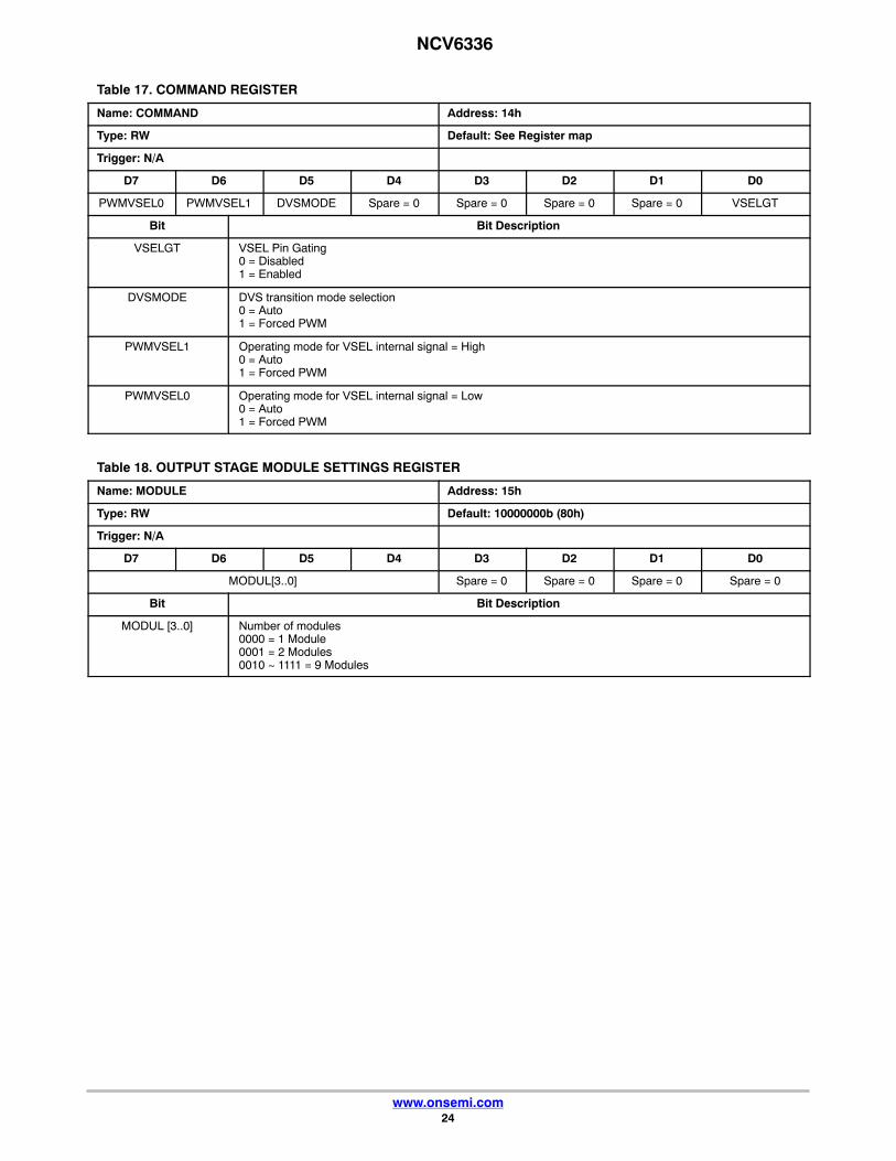
Table 17. COMMAND REGISTER
Name: COMMAND Address: 14h
Type: RW Default: See Register map
Trigger: N/A
D7 D6 D5 D4 D3 D2 D1 D0
PWMVSEL0 PWMVSEL1 DVSMODE Spare = 0 Spare = 0 Spare = 0 Spare = 0 VSELGT
Bit Bit Description
VSELGT VSEL Pin Gating0 = Disabled1 = Enabled
DVSMODE DVS transition mode selection0 = Auto1 = Forced PWM
PWMVSEL1 Operating mode for VSEL internal signal = High0 = Auto1 = Forced PWM
PWMVSEL0 Operating mode for VSEL internal signal = Low0 = Auto1 = Forced PWM
Table 18. OUTPUT STAGE MODULE SETTINGS REGISTER
Name: MODULE Address: 15h
Type: RW Default: 10000000b (80h)
Trigger: N/A
D7 D6 D5 D4 D3 D2 D1 D0
MODUL[3..0] Spare = 0 Spare = 0 Spare = 0 Spare = 0
Bit Bit Description
MODUL [3..0] Number of modules0000 = 1 Module0001 = 2 Modules0010 ~ 1111 = 9 Modules
NCV6336
www.onsemi.com25
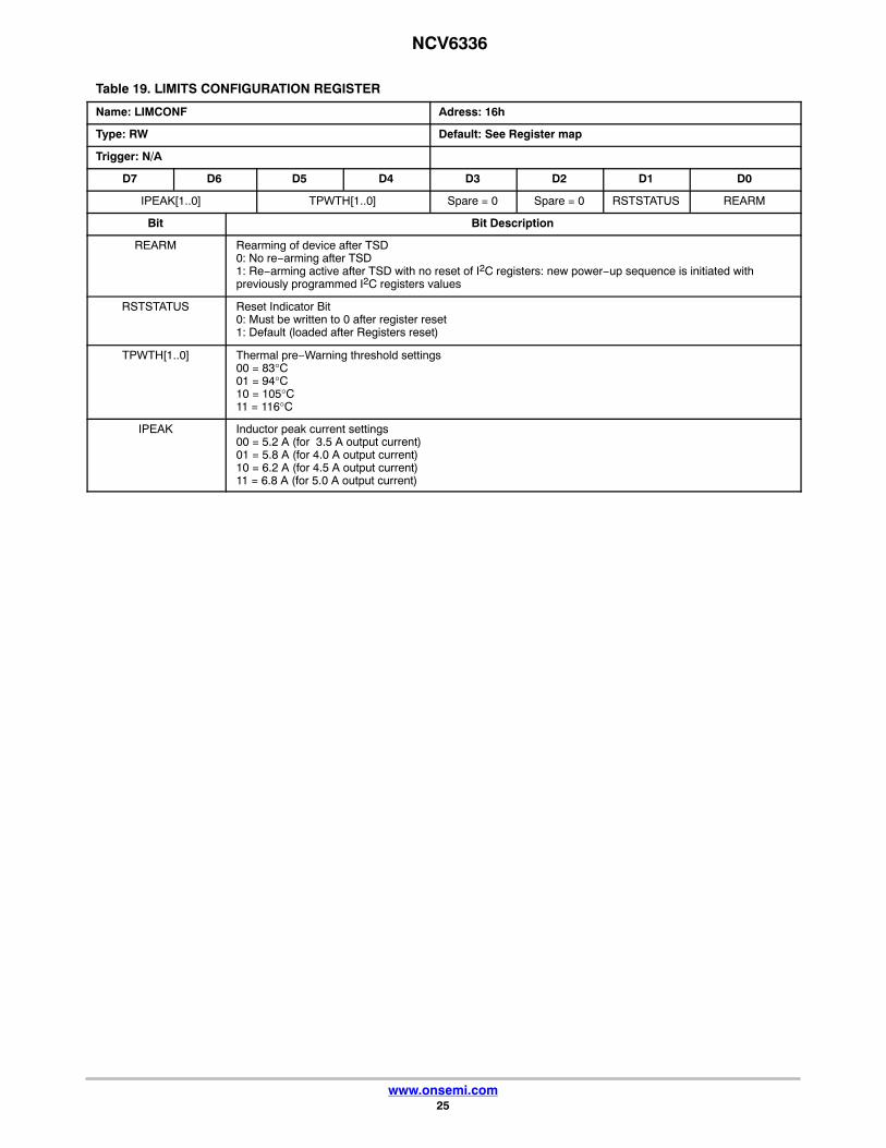
Table 19. LIMITS CONFIGURATION REGISTER
Name: LIMCONF Adress: 16h
Type: RW Default: See Register map
Trigger: N/A
D7 D6 D5 D4 D3 D2 D1 D0
IPEAK[1..0] TPWTH[1..0] Spare = 0 Spare = 0 RSTSTATUS REARM
Bit Bit Description
REARM Rearming of device after TSD0: No re−arming after TSD1: Re−arming active after TSD with no reset of I2C registers: new power−up sequence is initiated withpreviously programmed I2C registers values
RSTSTATUS Reset Indicator Bit 0: Must be written to 0 after register reset1: Default (loaded after Registers reset)
TPWTH[1..0] Thermal pre−Warning threshold settings00 = 83°C01 = 94°C10 = 105°C11 = 116°C
IPEAK Inductor peak current settings00 = 5.2 A (for 3.5 A output current)01 = 5.8 A (for 4.0 A output current)10 = 6.2 A (for 4.5 A output current)11 = 6.8 A (for 5.0 A output current)
NCV6336
www.onsemi.com26
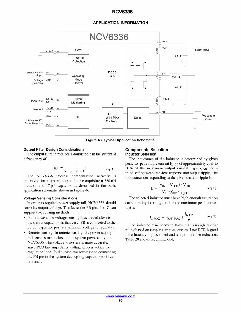
APPLICATION INFORMATION
Figure 46. Typical Application Schematic
330 nH
47 uF
ProcessorCore
NCV6336
I2C
ThermalProtection
Processor I2CControl Interface
OperatingMode
Control
OutputMonitoring
VoltageSelection
Interrupt
Power Fail
DCDC5 A
Supply Input
DCDC2.74 MHzController
Sense
Enable ControlInput
4.7 uF
SDA
SCL
AGND
PGNDINTB
PGNDPG
VSEL
EN
Core
SW
PVIN
PGND
FB
D2E1B4
A2
A1
B3
B2
B1
A3
D3D4E3E4
C1C2C3C4
A4
E2
D1 AVIN
Output Filter Design ConsiderationsThe output filter introduces a double pole in the system at
a frequency of:
fLC �1
2 � � � L � C� (eq. 1)
The NCV6336 internal compensation network isoptimized for a typical output filter comprising a 330 nHinductor and 47 �F capacitor as described in the basicapplication schematic shown in Figure 46.
Voltage Sensing ConsiderationsIn order to regulate power supply rail, NCV6336 should
sense its output voltage. Thanks to the FB pin, the IC cansupport two sensing methods:• Normal case: the voltage sensing is achieved close to
the output capacitor. In that case, FB is connected to theoutput capacitor positive terminal (voltage to regulate).
• Remote sensing: In remote sensing, the power supplyrail sense is made close to the system powered by theNCV6336. The voltage to system is more accurate,since PCB line impedance voltage drop is within theregulation loop. In that case, we recommend connectingthe FB pin to the system decoupling capacitor positiveterminal.
Components SelectionInductor Selection
The inductance of the inductor is determined by givenpeak−to−peak ripple current IL_PP of approximately 20% to50% of the maximum output current IOUT_MAX for atrade−off between transient response and output ripple. Theinductance corresponding to the given current ripple is:
L ��VIN � VOUT
� � VOUT
VIN � fSW � IL_PP
(eq. 2)
The selected inductor must have high enough saturationcurrent rating to be higher than the maximum peak currentthat is
IL_MAX � IOUT_MAX IL_PP
2(eq. 3)
The inductor also needs to have high enough currentrating based on temperature rise concern. Low DCR is goodfor efficiency improvement and temperature rise reduction.Table 20 shows recommended.
NCV6336
www.onsemi.com27
Table 20. INDUCTOR SELECTION
Supplier Part #Value(�H)
Size (mm)(L x l x T) (mm)
SaturationCurrent Max (A)
DCR Max at 25�C(m�)
Cyntec PIFE20161B−R33MS−11 0.33 2.0 x 1.6 x 1.2 4.0 33
Cyntec PIFE25201B−R33MS−11 0.33 2.5 x 2.0 x 1.2 5.2 17
Cyntec PIFE32251B−R33MS−11 0.33 3.2 x 2.5 x 1.2 6.5 14
TOKO DFE201612P−H−R30M 0.30 2.0 x 1.6 x 1.2 4.8 29
TOKO DFE252012P−H−R33M 0.33 2.5 x 2.0 x 1.2 5.2 24
TOKO FDSD0412−H−R33M 0.33 4.2 x 4.2 x 1.2 7.5 19
TDK VLS252012HBX−R33M 0.33 2.5 x 2.0 x 1.2 5.3 25
TDK SPM5030T−R35M 0.35 7.1 x 6.5 x 3.0 14.9 4
Output Capacitor SelectionThe output capacitor selection is determined by output
voltage ripple and load transient response requirement. Forhigh transient load performance high output capacitor valuemust be used. For a given peak−to−peak ripple current IL_PPin the inductor of the output filter, the output voltage rippleacross the output capacitor is the sum of three componentsas below.
VOUT_PP VOUT_PP(C) VOUT_PP(ESR) VOUT_PP(ESL),
(eq. 4)
Where VOUT_PP(C) is a ripple component by an equivalenttotal capacitance of the output capacitors, VOUT_PP(ESR) isa ripple component by an equivalent ESR of the outputcapacitors, and VOUT_PP(ESL) is a ripple component by anequivalent ESL of the output capacitors. In PWM operationmode, the three ripple components can be obtained by
VOUT_PP(C) �IL_PP
8 � C � fSW
, (eq. 5)
and
VOUT_PP(ESR) � IL_PP � ESR (eq. 6)
VOUT_PP(ESL) �ESL
ESL L� VIN (eq. 7)
and the peak−to−peak ripple current is
IL_PP ��VIN � VOUT
� � VOUT
VIN � fSW � L(eq. 8)
In applications with all ceramic output capacitors, themain ripple component of the output ripple is VOUT_PP(C).So that the minimum output capacitance can be calculatedregarding to a given output ripple requirement VOUT_PP inPWM operation mode.
CMIN �IL_PP
8 � VOUT_PP � fSW
(eq. 9)
Input Capacitor SelectionOne of the input capacitor selection guides is the input
voltage ripple requirement. To minimize the input voltageripple and get better decoupling in the input power supplyrail, ceramic capacitor is recommended due to low ESR andESL. The minimum input capacitance regarding to the inputripple voltage VIN_PP is
CIN_MIN �IOUT_MAX � �D � D2�
VIN_PP � fSW
(eq. 10)
where
D �VOUT
VIN
(eq. 11)
In addition, the input capacitor needs to be able to absorbthe input current, which has a RMS value of
IIN_RMS � IOUT_MAX � D � D2� (eq. 12)
The input capacitor also needs to be sufficient to protectthe device from over voltage spike, and normally at least4.7 �F capacitor is required. The input capacitor should belocated as close as possible to the IC. All PGNDs areconnected together to the ground terminal of the input capwhich then connects to the ground plane. All PVIN areconnected together to the Vbat terminal of the input capwhich then connects to the Vbat plane.
Electrical Layout ConsiderationsGood electrical layout is a key to ensuring proper
operation, high efficiency, and noise reduction. Electricallayout guidelines are:• Use wide and short traces for power paths (such as
PVIN, VOUT, SW, and PGND) to reduce parasiticinductance and high−frequency loop area. It is alsogood for efficiency improvement.
• The device should be well decoupled by input capacitorand input loop area should be as small as possible toreduce parasitic inductance, input voltage spike, andnoise emission.
• SW node should be a large copper, but compactbecause it is also a noise source.
NCV6336
www.onsemi.com28
• It would be good to have separated ground planes forPGND and AGND and connect the two planes at onepoint. Try best to avoid overlap of input ground loopand output ground loop to prevent noise impact onoutput regulation.
• Arrange a “quiet” path for output voltage sense, andmake it surrounded by a ground plane.
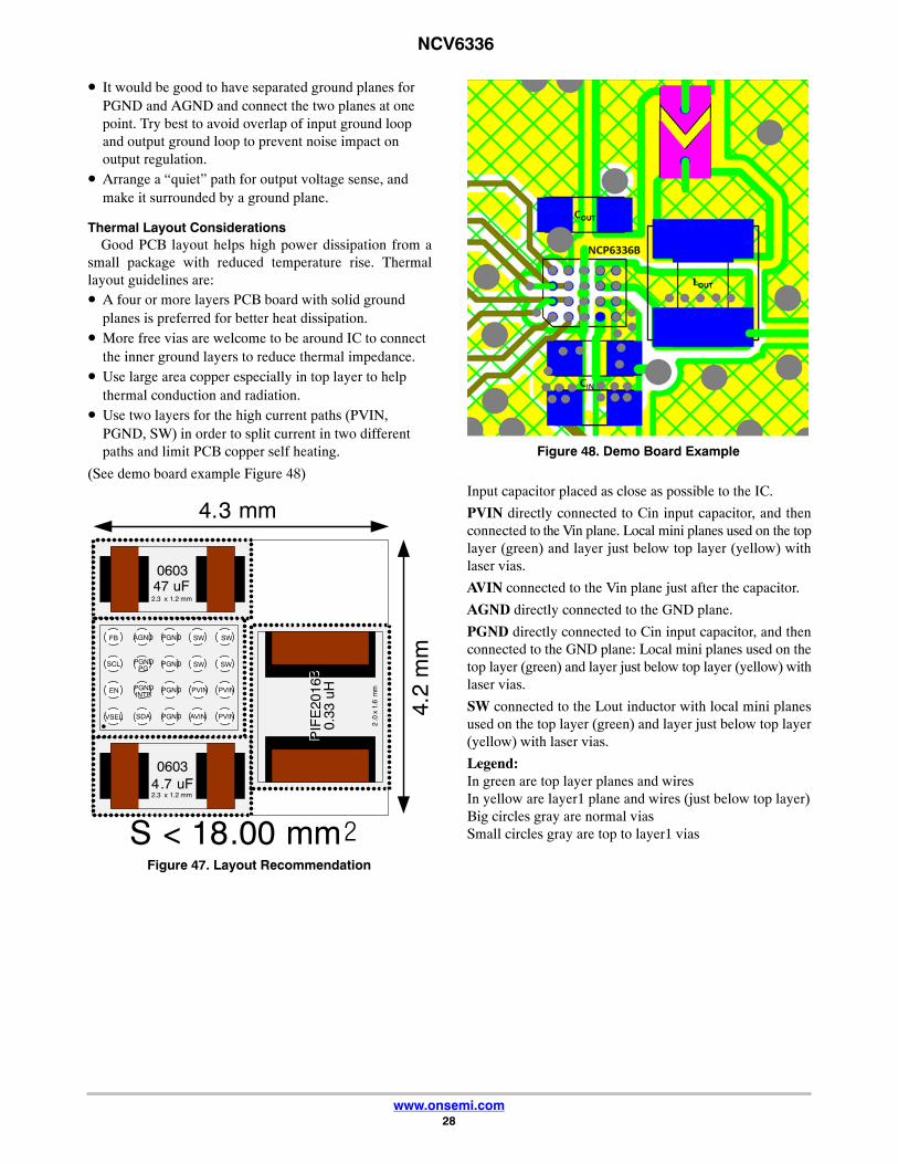
Thermal Layout ConsiderationsGood PCB layout helps high power dissipation from a
small package with reduced temperature rise. Thermallayout guidelines are:• A four or more layers PCB board with solid ground
planes is preferred for better heat dissipation.• More free vias are welcome to be around IC to connect
the inner ground layers to reduce thermal impedance.• Use large area copper especially in top layer to help
thermal conduction and radiation.• Use two layers for the high current paths (PVIN,
PGND, SW) in order to split current in two differentpaths and limit PCB copper self heating.
(See demo board example Figure 48)
Figure 47. Layout Recommendation
4.2
mm
S < 18.00 mm�
06034.7 uF2.3 x 1.2 mm
060347 uF2.3 x 1.2 mm
0.33
uH
2.0
x1.
6m
m
PVINAVIN
SWSW
PVIN
PGND
PGNDINTB
SCL
EN PVINPGND
PGNDSDA
PGNDPG
VSEL
SWSWPGNDFB AGND
4.3 mm
PIF
E20
16B
PIF
E20
16B
Figure 48. Demo Board Example
Input capacitor placed as close as possible to the IC.
PVIN directly connected to Cin input capacitor, and thenconnected to the Vin plane. Local mini planes used on the toplayer (green) and layer just below top layer (yellow) withlaser vias.
AVIN connected to the Vin plane just after the capacitor.
AGND directly connected to the GND plane.
PGND directly connected to Cin input capacitor, and thenconnected to the GND plane: Local mini planes used on thetop layer (green) and layer just below top layer (yellow) withlaser vias.
SW connected to the Lout inductor with local mini planesused on the top layer (green) and layer just below top layer(yellow) with laser vias.
Legend:In green are top layer planes and wiresIn yellow are layer1 plane and wires (just below top layer)Big circles gray are normal viasSmall circles gray are top to layer1 vias
NCV6336
www.onsemi.com29
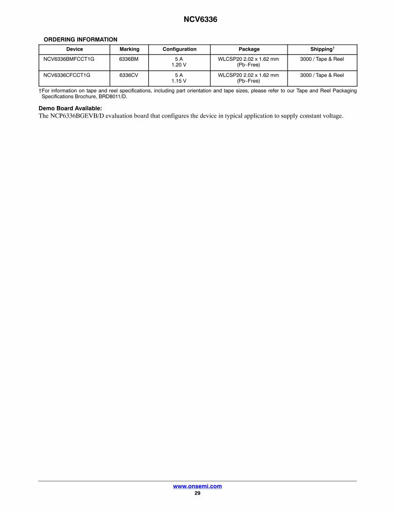
ORDERING INFORMATION
Device Marking Configuration Package Shipping†
NCV6336BMFCCT1G 6336BM 5 A1.20 V
WLCSP20 2.02 x 1.62 mm(Pb–Free)
3000 / Tape & Reel
NCV6336CFCCT1G 6336CV 5 A1.15 V
WLCSP20 2.02 x 1.62 mm(Pb–Free)
3000 / Tape & Reel
†For information on tape and reel specifications, including part orientation and tape sizes, please refer to our Tape and Reel PackagingSpecifications Brochure, BRD8011/D.
Demo Board Available:The NCP6336BGEVB/D evaluation board that configures the device in typical application to supply constant voltage.
WLCSP20, 1.62x2.02CASE 568AG
ISSUE DDATE 13 AUG 2013
SEATINGPLANE
0.10 C
NOTES:1. DIMENSIONING AND TOLERANCING PER
ASME Y14.5M, 1994.2. CONTROLLING DIMENSION: MILLIMETERS.3. COPLANARITY APPLIES TO THE SPHERICAL
CROWNS OF THE SOLDER BALLS.
2X
DIMA
MIN MAX−−−
MILLIMETERS
A1
D 1.62 BSCE
b 0.24 0.28
e 0.40 BSC
0.60
ÈÈÈÈ
D
E
A BPIN A1
REFERENCE
eA0.05 BC
0.03 C
0.05 C
20X b
4
C
B
A
0.10 C
A
A1
A2
C
0.17 0.23
2.02 BSC
SCALE 4:1
0.2520X
DIMENSIONS: MILLIMETERS
*For additional information on our Pb−Free strategy and solderingdetails, please download the ON Semiconductor Soldering andMounting Techniques Reference Manual, SOLDERRM/D.
SOLDERING FOOTPRINT*
0.40
0.40
0.10 C2X TOP VIEW
SIDE VIEW
BOTTOM VIEW
NOTE 3
e
RECOMMENDED
PACKAGEOUTLINE
1 2 3
PITCH
D
E
PITCH
A1
A2 0.33 0.39
e/2A = Assembly LocationWL = Wafer LotY = YearWW = Work Week� = Pb−Free Package
*This information is generic. Please refer todevice data sheet for actual part marking.Pb−Free indicator, “G” or microdot “ �”,may or may not be present.
GENERICMARKING DIAGRAM*
XXXXXXAWLYWW
�
DIE COAT(OPTIONAL)
DETAIL A
A2A3
DETAIL A
A3 0.02 0.04
MECHANICAL CASE OUTLINE
PACKAGE DIMENSIONS
ON Semiconductor and are trademarks of Semiconductor Components Industries, LLC dba ON Semiconductor or its subsidiaries in the United States and/or other countries.ON Semiconductor reserves the right to make changes without further notice to any products herein. ON Semiconductor makes no warranty, representation or guarantee regardingthe suitability of its products for any particular purpose, nor does ON Semiconductor assume any liability arising out of the application or use of any product or circuit, and specificallydisclaims any and all liability, including without limitation special, consequential or incidental damages. ON Semiconductor does not convey any license under its patent rights nor therights of others.
98AON82918EDOCUMENT NUMBER:
DESCRIPTION:
Electronic versions are uncontrolled except when accessed directly from the Document Repository.Printed versions are uncontrolled except when stamped “CONTROLLED COPY” in red.
PAGE 1 OF 1WLCSP20, 1.62X2.02
© Semiconductor Components Industries, LLC, 2019 www.onsemi.com
onsemi, , and other names, marks, and brands are registered and/or common law trademarks of Semiconductor Components Industries, LLC dba “onsemi” or its affiliatesand/or subsidiaries in the United States and/or other countries. onsemi owns the rights to a number of patents, trademarks, copyrights, trade secrets, and other intellectual property.A listing of onsemi’s product/patent coverage may be accessed at www.onsemi.com/site/pdf/Patent−Marking.pdf. onsemi reserves the right to make changes at any time to anyproducts or information herein, without notice. The information herein is provided “as−is” and onsemi makes no warranty, representation or guarantee regarding the accuracy of theinformation, product features, availability, functionality, or suitability of its products for any particular purpose, nor does onsemi assume any liability arising out of the application or useof any product or circuit, and specifically disclaims any and all liability, including without limitation special, consequential or incidental damages. Buyer is responsible for its productsand applications using onsemi products, including compliance with all laws, regulations and safety requirements or standards, regardless of any support or applications informationprovided by onsemi. “Typical” parameters which may be provided in onsemi data sheets and/or specifications can and do vary in different applications and actual performance mayvary over time. All operating parameters, including “Typicals” must be validated for each customer application by customer’s technical experts. onsemi does not convey any licenseunder any of its intellectual property rights nor the rights of others. onsemi products are not designed, intended, or authorized for use as a critical component in life support systemsor any FDA Class 3 medical devices or medical devices with a same or similar classification in a foreign jurisdiction or any devices intended for implantation in the human body. ShouldBuyer purchase or use onsemi products for any such unintended or unauthorized application, Buyer shall indemnify and hold onsemi and its officers, employees, subsidiaries, affiliates,and distributors harmless against all claims, costs, damages, and expenses, and reasonable attorney fees arising out of, directly or indirectly, any claim of personal injury or deathassociated with such unintended or unauthorized use, even if such claim alleges that onsemi was negligent regarding the design or manufacture of the part. onsemi is an EqualOpportunity/Affirmative Action Employer. This literature is subject to all applicable copyright laws and is not for resale in any manner.
PUBLICATION ORDERING INFORMATIONTECHNICAL SUPPORTNorth American Technical Support:Voice Mail: 1 800−282−9855 Toll Free USA/CanadaPhone: 011 421 33 790 2910
LITERATURE FULFILLMENT:Email Requests to: [email protected]
onsemi Website: www.onsemi.com
Europe, Middle East and Africa Technical Support:Phone: 00421 33 790 2910For additional information, please contact your local Sales Representative
◊