status of the cbm tof tdc development
DESCRIPTION
Status of the CBM ToF TDC Development. Detector Requirements TDC Core & Testchip Performance Architecture & Readout Concept Status and Submission Plans. Detector Requirements. Time Resolution< 25 ps Double Hit Resolution< 10 ns (better < 5 ns) Time over ThresholdYes - PowerPoint PPT PresentationTRANSCRIPT

EE- ASIC
Status of the CBM ToF TDC Development
Detector Requirements TDC Core & Testchip Performance Architecture & Readout Concept Status and Submission Plans

EE- ASIC
Detector Requirements
• Time Resolution < 25 ps• Double Hit Resolution < 10 ns (better < 5 ns)• Time over Threshold Yes• Power Consumption < 60 mW / Ch• Integration Level min. 4 Ch / Chip

EE- ASIC
Status of the CBM ToF TDC Development
Detector Requirements TDC Core & Testchip Performance Architecture & Readout Concept Status and Submission Plans
EE- ASIC
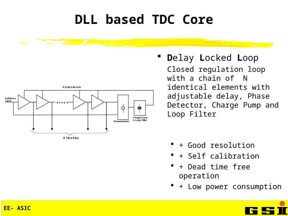
Delay Locked LoopClosed regulation loop with a chain of N identical elements with adjustable delay, Phase Detector, Charge Pump and Loop Filter
+ Good resolution + Self calibration + Dead time free operation + Low power consumption
Reference Clock
N Delay Elements
Phasedetector
Charge Pump & Loop Filter
N Time Bins
DLL based TDC Core

EE- ASIC
DLL structure with 64 DE 160MHz clock input Intrinsic bin size: ~ 50ps Additional components:
Hit-Reg, RO-Logic 1 Bit serial output
Size: 1525µm x 1525µm
Testchip DANTE DLL
870µm 210µm
Delay Chain
Loop Filter
Ref Clk
Phase Detector Charge PumpChip submitted in Feb 2007

EE- ASIC
DANTE DoubleBin DLL
20 40 60 80 100 1200
500000
1000000
1500000
2000000
2500000 Modell: GaussGleichung: y=y0 + (A/(w*sqrt(PI/2)))*exp(-2*((x-xc)/w)^2)
w 1.17816 ±0.0087corr. 28.76 ps ± 0.21ps
uncorr. 20.34 ps ± 0.15ps
Co
un
ts
# TimeBin
Power consumption DLL (Sim.) I = 3 mA @1.8V => 5.4 mW
Power consumption DANTE (Mea.) I = 18 mA @1.8V => 32.4 mW
Resolution σuc = 20.34 ps ± 0.15ps
DNL: (+ 0.34 / - 0.38) LSB INL: (+ 0.51 / - 0.49) LSB
DNL PLOT DANTE-DLL Vcore=1.8V, f=160MHz
-1,00
-0,80
-0,60
-0,40
-0,20
0,00
0,20
0,40
0,60
0,80
1,00
1 17 33 49 65 81 97 113
TIME BIN #
LS
B
+0.49 LSB -0.39 LSB
DNL =

EE- ASIC
Status of the CBM ToF TDC Development
Detector Requirements TDC Core & Testchip Performance Architecture & Readout Concept Status and Submission Plans

EE- ASIC
Architecture & Readout Concept
• 4 Channels with LVDS Input
• 2 Events / Clock Cycle → Double Hit Resolution: ≤ 3.1 ns
• Time over Threshold Measurement
• Serial Data Communication

EE- ASIC
Timing and Synchronisation
• CBM System Clock : 250 MHz ( TSys = 4 ns )
• DLL Clock: 156.25 MHz ( = 5/8 * 250 MHz )• Intrinsic Time Binning : 50 ps• 12 Bit Timestamp Counter
• TEpoche = 26.2144 µs
• For Synchronisation: 2048 * TSys = 5 * TEpoche
• Synchronisation Intervall : TSync = 131.072 µs
EE- ASIC
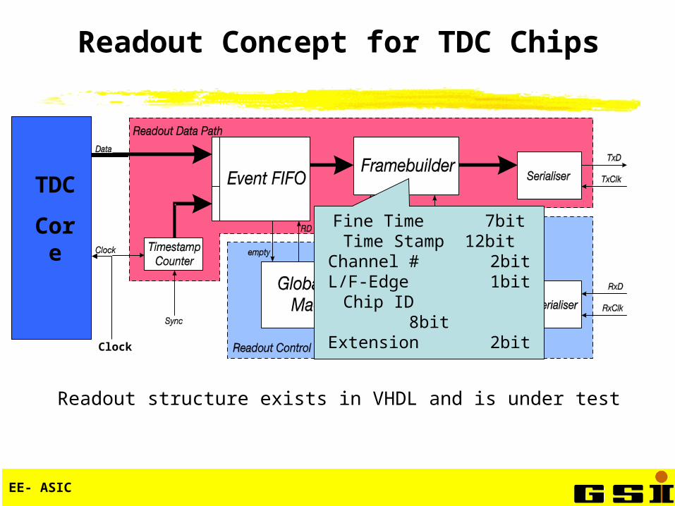
Readout Concept for TDC Chips
Readout structure exists in VHDL and is under test
TDC
Core
Clock
Fine Time 7bitTime Stamp 12bitChannel # 2bitL/F-Edge 1bitChip ID 8bitExtension 2bit

EE- ASIC
Status of the CBM ToF TDC Development
Detector Requirements TDC Core & Testchip Performance Architecture & Readout Concept Status and Submission Plans

EE- ASIC
Status and Submission Plans
• Schematic and Layout for Time Core• Parasitic Simulation still missing• Design of Readout Logic• Submission planed for summer 2008

EE- ASIC
Thank you for your attention