stackup planning pt1 pcbd-june2015 - icd | · pdf file · 2015-10-14board stackup....
TRANSCRIPT


46
by Barry Olney
BEYOND DESIGN
Signal Integrity, Part 3
column
In last month’s column, I looked at the ef-fects of crosstalk, timing and skew on signal quality. This month, I will continue to discuss signal integrity, in particular where most de-signers go wrong and how to avoid the com-mon pitfalls.
Digital designs become less forgiving as edge rates and frequencies increase. What used to work in the past may not work now, and a different approach to layout may be necessary. Also, there may be many issues that aren’t at first apparent, but affect the reliable performance of the product. Signal and power integrity issues, for instance, often manifest themselves as inter-mittent operation, which can be very difficult to nail. So it is best to find these issues during the design process and eliminate them at the source, rather than apply a Band-Aid solution after production.
I have analyzed many high-speed boards over the past 15 years and have established a process that I follow in order to achieve effec-
-quire expensive analysis tools, but rather com-mon sense. I find that a large percentage of is-sues can be detected just by eye-balling the de-sign—simulators don’t pick up everything.
The first thing to look at, of course, is the board stackup. The substrate is the most impor-tant component of the assembly and needs to be planned correctly in order to maintain con-sistent impedance across layers, avoid uninten-tional signal coupling and reduce electromag-netic emissions. In Part 1 of this series, I set out the basic rules for stackup planning that should be adhered to. The most important being: All signal layers should be adjacent to, and closely coupled to, an uninterrupted reference plane,
48
creating a clear return path and eliminating broadside crosstalk. Figure 1 illustrates a good stackup in this regard.
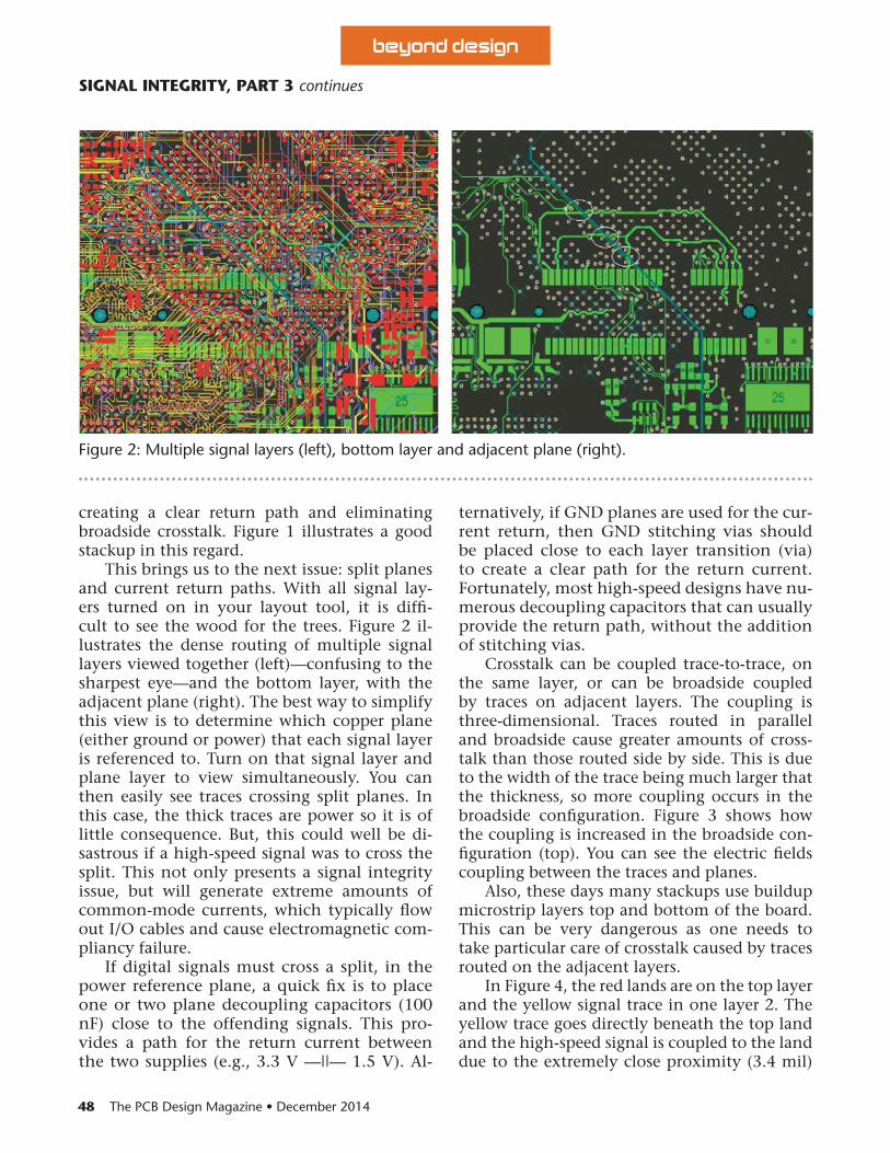
This brings us to the next issue: split planes and current return paths. With all signal lay-ers turned on in your layout tool, it is diffi-cult to see the wood for the trees. Figure 2 il-lustrates the dense routing of multiple signal layers viewed together (left)—confusing to the sharpest eye—and the bottom layer, with the adjacent plane (right). The best way to simplify this view is to determine which copper plane (either ground or power) that each signal layer is referenced to. Turn on that signal layer and plane layer to view simultaneously. You can then easily see traces crossing split planes. In this case, the thick traces are power so it is of little consequence. But, this could well be di-sastrous if a high-speed signal was to cross the split. This not only presents a signal integrity issue, but will generate extreme amounts of common-mode currents, which typically flow out I/O cables and cause electromagnetic com-pliancy failure.
If digital signals must cross a split, in the power reference plane, a quick fix is to place one or two plane decoupling capacitors (100 nF) close to the offending signals. This pro-vides a path for the return current between
-
-
be placed close to each layer transition (via) to create a clear path for the return current. Fortunately, most high-speed designs have nu-merous decoupling capacitors that can usually provide the return path, without the addition of stitching vias.
Crosstalk can be coupled trace-to-trace, on the same layer, or can be broadside coupled by traces on adjacent layers. The coupling is three-dimensional. Traces routed in parallel and broadside cause greater amounts of cross-talk than those routed side by side. This is due to the width of the trace being much larger that the thickness, so more coupling occurs in the broadside configuration. Figure 3 shows how the coupling is increased in the broadside con-figuration (top). You can see the electric fields coupling between the traces and planes.
Also, these days many stackups use buildup microstrip layers top and bottom of the board. This can be very dangerous as one needs to take particular care of crosstalk caused by traces routed on the adjacent layers.
In Figure 4, the red lands are on the top layer and the yellow signal trace in one layer 2. The yellow trace goes directly beneath the top land and the high-speed signal is coupled to the land due to the extremely close proximity (3.4 mil)
beyond design
SIGNAL INTEGRITY, PART 3 continues

49
beyond design
SIGNAL INTEGRITY, PART 3 continues
of signal layers. Figure 5 shows part of the stack-up cross-section in the ICD Stackup Planner. In this case, both signal layers are referenced to the
Recently, I analyzed a design where the
lands on the top layer connected to a WiFi module and the signal on layer 2 injected a ran-dom pulse into the module via this close cou-pling. The symptom was that the product ran for about an hour then all of a sudden missed a beat and had to be rebooted. Once this issue was fixed, the product then ran reliably for days without failure. Simple fix, but hard to find!
Crosstalk is also typically picked up on long parallel trace segments. These can be on the same layer or may also be broadside coupled from the adjacent layer. Fortunately, source synchronous busses have a unique immunity to crosstalk, provided that the ringing has settled by the time the bus is sampled by the clock. So there are two issues here:
1. Keep parallel trace segments as short as possible to reduce coupling (crosstalk) unless you are using a synchronous bus. Space the groups of signals (e.g., address and data) by three times the trace width.2. Always route the clock (or strobe) to the longest delay of the group of signals. This allows the data to settle before it is read by the clock.
In a previous column, Matched Length Does , I discussed
matched length routing and how matched length does not necessarily mean matched de-lay. Flight time (propagation delay) varies de-pending on the dielectric material that the sig-nal propagates in.
Where c is the speed of light and “Er eff” is the effective dielectric constant.
In a microstrip configuration, the effective dielectric constant is dependent on the FR-4
50
material, the solder mask and the air above. In a stripline configuration, it is dependent on the FR-4 material above and below the trace. So, microstrip signals tend to travel faster than stripline as the effective Er is smaller. Also, an accordion or serpentine pattern will be faster than the equivalent straight trace, due to for-ward crosstalk. So this is not a simple calcula-tion and requires a simulator to compare delays on different layers of the substrate.
Rather than matched length, one needs to compare the actual delay as the signals prop-agate through different materials in the sub-strate. This is done in order to determine the skew between clocks (or strobes) and the groups of signals they control. If you must assess using matched length, tighten the tolerance as this will still reduce the skew.
Routing critical signals between the planes can reduce emissions by 10 dB or more. There are four constraints to keep in mind:
1. Keep the mark-to-space ratio of the waveform equal as this eliminates all the even harmonics. 2. Route high-speed signals out from the centre of the board where possible, as any radiation will be in the opposite direction and will tend to cancel.
3. Route high-speed signals between the planes, fanout close to the driver (200 mils) dropping to an inner plane and route back up to the load again with a short fanout. 4. Use the same reference plane for the return signals, as this reduces the loop area and hence radiation.
Embedding signals between the planes also reduces susceptibility to radiation, as well as providing ESD protection. So, not only does this prevent noise from being radiated, but it also reduces the possibility of being affected by an external noise source.
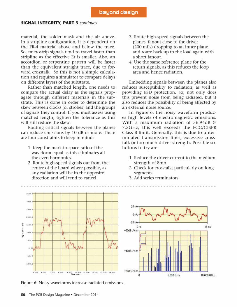
In Figure 6, the noisy waveform produc-es high levels of electromagnetic emissions. With a maximum radiation of 56.94dB @ 7.5GHz, this well exceeds the FCC/CISPR Class B limit. Generally, this is due to unter-minated transmission lines, excessive cross-talk or too much driver strength. Possible so-lutions to try are:
1. Reduce the driver current to the medium 2. Check for crosstalk, particularly on long segments.3. Add series terminators.
SIGNAL INTEGRITY, PART 3 continues
beyond design

51
Placing series terminators from the begin-ning will not hurt, as they can always be re-placed by zero ohm resistors if not needed—not a great expense, but this can alleviate ringing problems. Terminators do however slow down the signal rise time.
If this noise is not constrained, at the source, then it will be coupled into nearby victim trac-es (crosstalk) and radiate to create more EMI. Apart from the issues of EMI, signal integrity and crosstalk, this noise can cause intermittent operation of the product due to timing glitch-es and interference, dramatically reducing the products reliability.
Points to Remember: edge rates and frequencies increase.
-stance, often manifest themselves as inter-mittent operation.
-up. All signal layers should be adjacent to and closely coupled to an uninterrupted reference plane, creating a clear return path and eliminating broadside crosstalk. Figure 1 illustrates a good stackup in this regard.
is to determine which copper plane (either ground or power) each signal layer is ref-erenced to. Then turn on that signal layer and plane layer to view alongside.
power reference plane, decoupling capaci-tors can be placed close to the offending signals to provide a path for the return cur-rent between the two supplies.
-
placed close to each layer transition.
the same layer, or can be broadside cou-pled by traces on adjacent layers.
cause greater amounts of crosstalk than those routed side by side.
-
gerous, as one must take particular care of crosstalk caused by traces routed on the adjacent layers.
possible to reduce coupling crosstalk.
-lay of the group of signals. This allows the data to settle before it is read by the clock.
-tric material that the signal propagates in.
the tolerance as this will still reduce the skew.
can reduce emissions by 10dB or more.
also reduces susceptibility to radiation, as well as providing ESD protection.
the driver strength to the medium cur-rent, check for crosstalk, particularly on long segments, or add series terminators.PCBDESIGN
References1. Barry Olney: Beyond Design: Practical Sig-
nal Integrity; Beyond Design: Pre-Layout Sim-ulation; Intro to Board-Level Simulation and the PCB Design Process; Beyond Design: Im-pedance Matching: Terminations; Beyond De-
Matched Delay
2. Howard Johnson: High-Speed Signal Propagation
distributed globally by www.altium.com
.
SIGNAL INTEGRITY, PART 3 continues
beyond design