stability of operational amplifiersextras.springer.com/2006/978-0-387-25746-4/chapter_05.pdf ·...
TRANSCRIPT

Willy Sansen 10-05 051
Stability ofOperational amplifiers
Willy Sansen
KULeuven, ESAT-MICASLeuven, Belgium
Willy Sansen 10-05 052
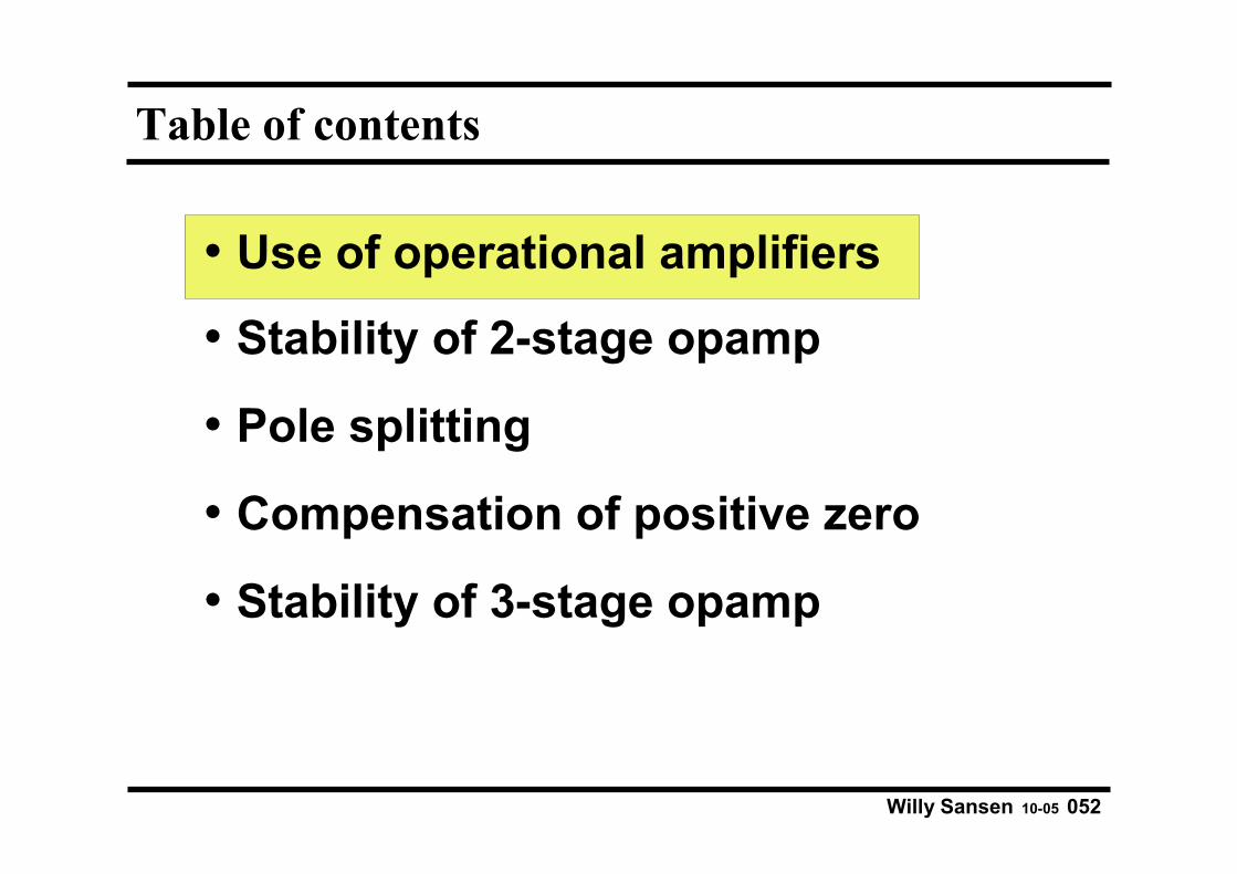
Table of contents
• Use of operational amplifiers
• Stability of 2-stage opamp
• Pole splitting
• Compensation of positive zero
• Stability of 3-stage opamp

Willy Sansen 10-05 053
Operational amplifiers do operations
+- vOUT
RF
R1
R2
R3
v1
v2
v3
RF
vOUT- = +R1
v1
R2
v2
R3
v3+
Requires High gainHigh speedLow noiseLow power
Opamp specs : Voltage gain is largeDifferential input voltage ≈ 0Input current = 0Bandwidth is highGainbandwidth GBW is very, very high
Willy Sansen 10-05 054
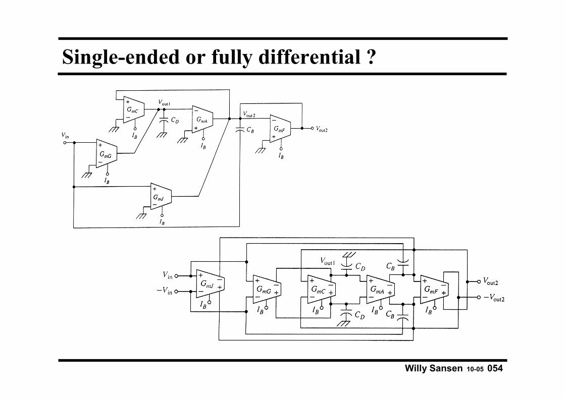
Single-ended or fully differential ?
Willy Sansen 10-05 055
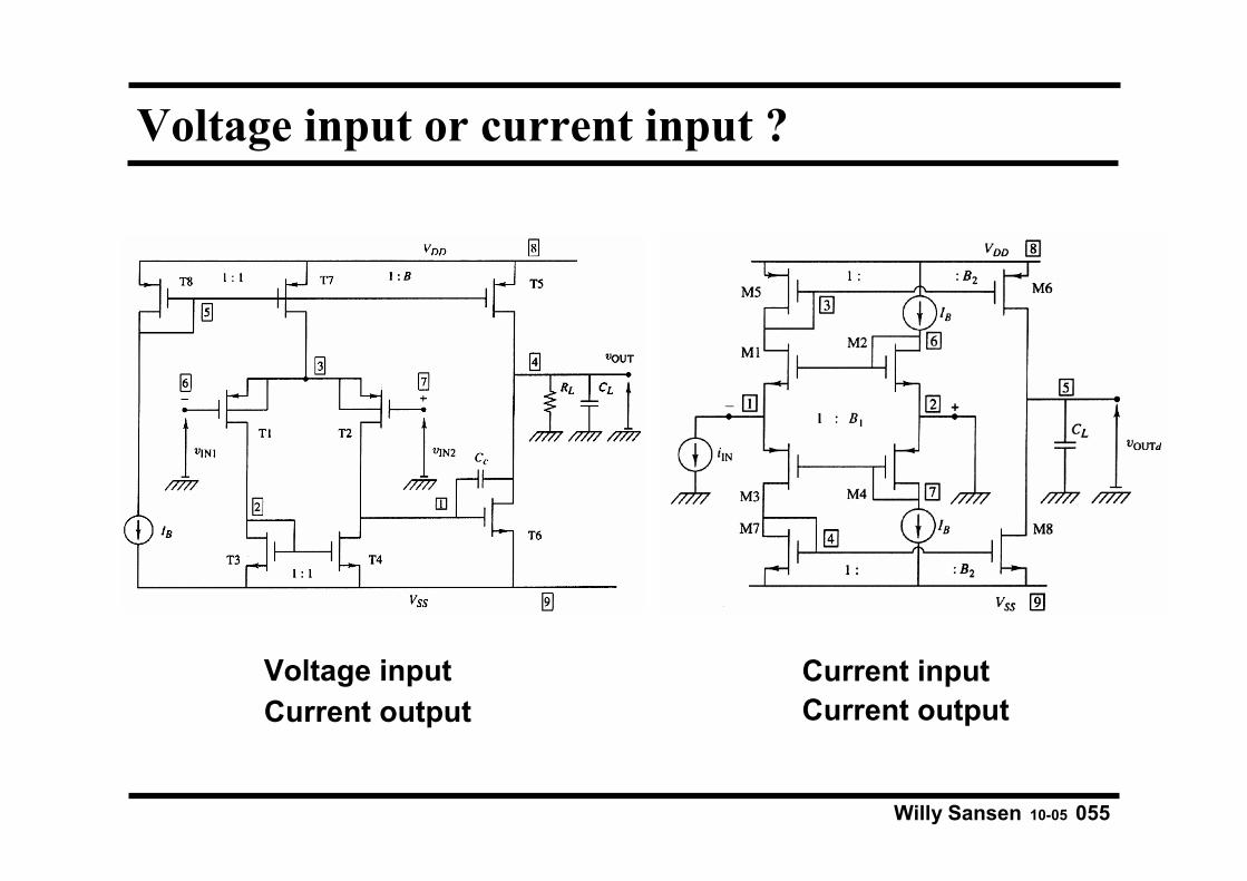
Voltage input or current input ?
Voltage inputCurrent output
Current input Current output

Willy Sansen 10-05 056
Classification
Operational amplifier
Opamp OTA OCA CM ampOperational
Transconduct.amplifier
OperationalCurrent amplifier
CurrentMode
amplifier
+-
+-
+-
+-
Av =vOUTvIN
Ag =iOUTvIN
Ai =iOUTiIN
Ar =vOUTiIN
Av = = Ag RL = Ai = ArRLRS
1RS
GBW
Willy Sansen 10-05 057
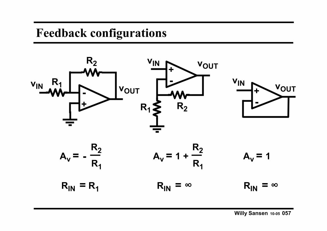
Feedback configurations
+- vOUT
R2
R1vIN
Av = -R1
R2
+-
vOUT
R2R1
vIN+-
vOUT
vIN
Av = 1 +R1
R2
RIN = R1 RIN = ∞ RIN = ∞
Av = 1
Willy Sansen 10-05 058
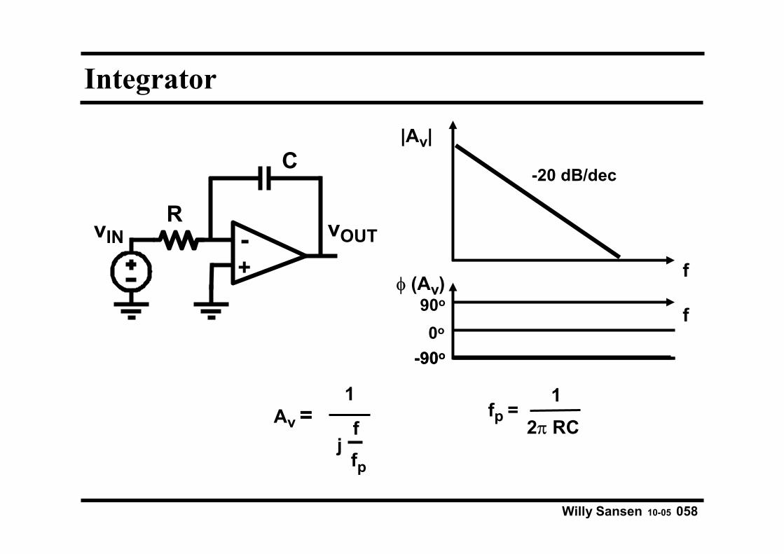
Integrator
|Av|
f
f
-20 dB/dec
φ (Av)
-90o
0o
90o
+- vOUT
RvIN
C
-90o
Av = fp = 1
2π RC
fp
fj
1

Willy Sansen 10-05 059
Low-pass filter
|Av|
fp f
f
-20 dB/dec
φ (Av)
-90o
0o
90o
+- vOUT
R2
R1vIN
C
R1
R2
-90o
Av = fp = 1
2π R2C
fp
f
Av0
(1 + j )
Av0Av0 = -

Willy Sansen 10-05 0510
High-pass filter
+- vOUT
R2
R1vIN
L
R1
R2 Av = Av0
fp
f(1 + j )
Av0 = -
|Av|
fp f
f
20 dB/dec
φ (Av)
-90o
0o
90o
-90o
fp = R2
2π L
fp
fj
Av0

Willy Sansen 10-05 0511
High-pass filter
+-
vOUT
R2R1
vIN
Av0 = 1 +R1
R2
C
|Av|
φ (Av) fz f
f
-90o
0o
20 dB/dec
90o
Av = AV0 (1 + j ) fz = 1
2π RCfz
f R = R1//R2 = R1+R2
R1R2
Av0
Willy Sansen 10-05 0512
Low-pass filter with finite attenuation
+-
vOUT
R2R1
vIN
Av0 = 1 +R1
R2
|Av|
φ (Av) fz f
f
-90o
0o
-20 dB/dec
90o
fz = 1
2π RCR = R1+R2
Av0C
Av = Av0
fz
fj
fz
f(1 + j )
Willy Sansen 10-05 0513
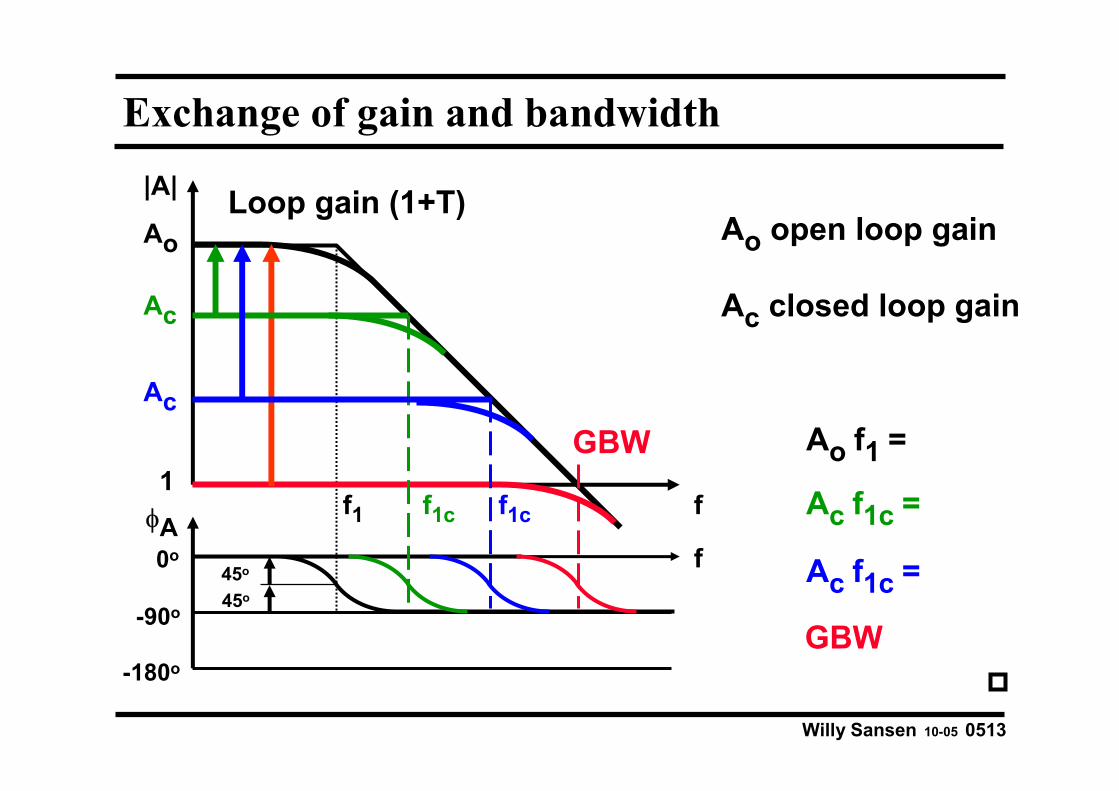
Exchange of gain and bandwidth
-180o
-90o
0o
Ao
1
|A|
f1 f
Loop gain (1+T)Ao open loop gain
Ac closed loop gain
GBW Ao f1 =
Ac
f1c Ac f1c =
Ac
f1c
Ac f1c =
GBW
45o
45o
fφA
Willy Sansen 10-05 0514
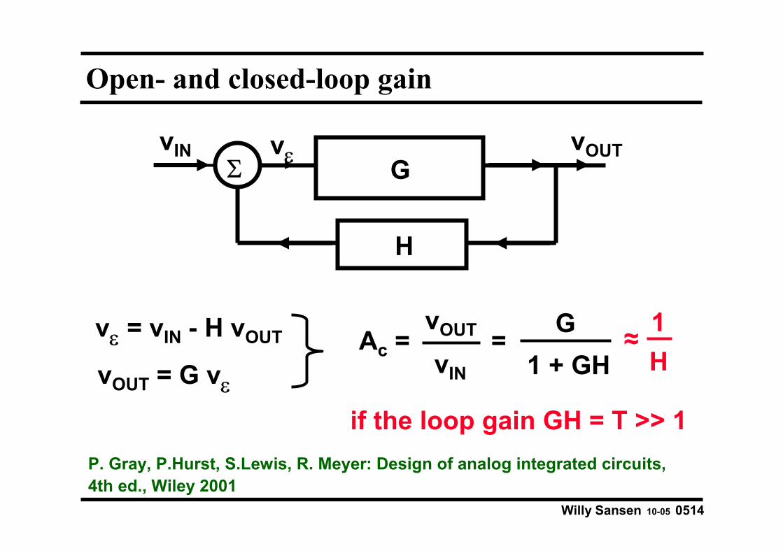
Open- and closed-loop gain
G
H
Σ
if the loop gain GH = T >> 1
vε = vIN - H vOUT
1 + GH≈ 1
H
vIN vOUTvε
vOUT = G vε
vOUT
vIN= G
P. Gray, P.Hurst, S.Lewis, R. Meyer: Design of analog integrated circuits,4th ed., Wiley 2001
Ac =

Willy Sansen 10-05 0515
What makes an opamp an opamp ?
Operational amplifier :Single-pole amplifierHigh impedance = high gainExchange Gain-BandwidthStable for all gain values
Wideband amplifier :Multiple-pole amplifierLow impedances at nodesWide BandwidthStable for one gain only
+vout
vin
CL
vin
vout

Willy Sansen 10-05 0516
Single-pole system
-180o
-90o
0o
Ao
Ac=1
|A|
f1f
Ao open loop gain
Closed loop gain Ac = 1
φA
f
-20 dB/dec
open loop closed loop
GBW
PM phase marginPM
loop gain

Willy Sansen 10-05 0517
Two-pole system
-180o
-90o
0o
Ao
Ac=1
|A|
f1 f2 fφA
Ao open loop gain
Closed loop gain Ac = 1-20 dB/dec
-40 dB/dec
open closed loop
vIN+-
vOUTloop gain
PM phase marginPM
GBW
Willy Sansen 10-05 0518
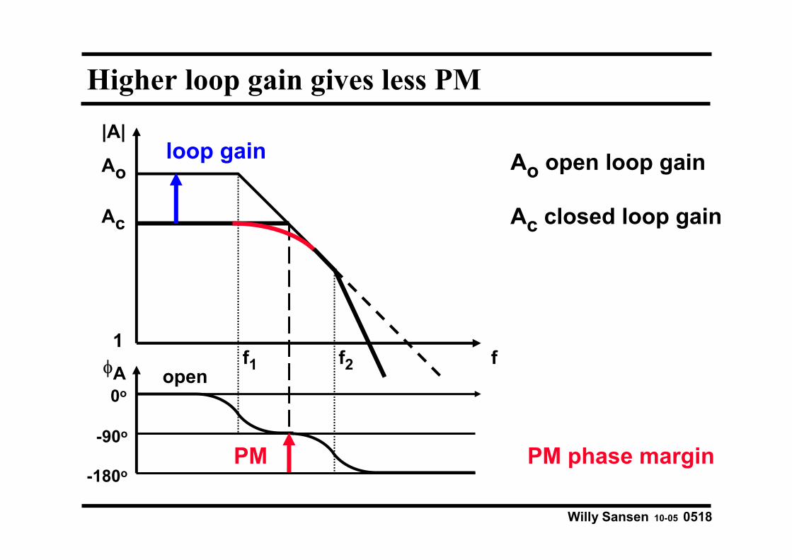
Higher loop gain gives less PM
-180o
-90o
0o
Ao
Ac
1
|A|
f1 f2 f
loop gain Ao open loop gain
Ac closed loop gain
PM phase marginPM
φA open

Willy Sansen 10-05 0519
Higher loop gain gives less PM
-180o
-90o
0o
Ao
Ac
1
|A|
f1 f2 f
loop gain Ao open loop gain
Ac closed loop gain
PM phase marginPM
φA open
Willy Sansen 10-05 0520
Higher loop gain gives less PM
-180o
-90o
0o
Ao
Ac
1
|A|
f1 f2 f
loop gain Ao open loop gain
Ac closed loop gain
PM phase marginPM
φA open

Willy Sansen 10-05 0521
Higher loop gain gives less PM
-180o
-90o
0o
Ao
Ac=1
|A|
f1 f2 f
loop gain Ao open loop gain
Ac closed loop gain
PM phase marginPM
Worst case for Ac = 1
φA open

Willy Sansen 10-05 0522
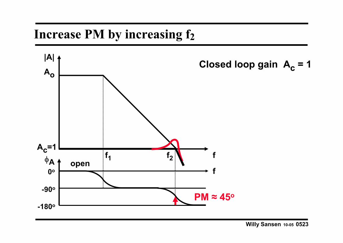
Increase PM by increasing f2 : low f2
-180o
-90o
0o
Ao
Ac=1
|A|
f1 f2 f
PM ≈ 0o
φA
Closed loop gain Ac = 1
fopen
Willy Sansen 10-05 0523
Increase PM by increasing f2
-180o
-90o
0o
Ao
Ac=1
|A|
f1 f2 f
PM ≈ 45o
φA
Closed loop gain Ac = 1
fopen

Willy Sansen 10-05 0524
Set PM by setting f2 ≈ 3 GBW
-180o
-90o
0o
Ao
Ac=1
|A|
f1 f2 f
PM ≈ 70o
φA
Closed loop gain Ac = 1
f
GBW f2 ≈ 3 GBW
open

Willy Sansen 10-05 0525
Calculate PM for f2 ≈ 3 GBW
Open loop gain A =
Closed loop gain Ac = ≈
Ao
(1 + j )(1 + j )ff1
ff2
A1+A
1
1 + j + j2 f2GBW f2
fGBW
1
1 + j 2ζ + j2 f2
fr2
ffr
≈
ζ is the damping (=1/2Q)fr is the resonant frequency
vIN+-
vOUT
Ac = 1
AH = 1

Willy Sansen 10-05 0526
Relation PM, damping and f2/GBW
fr = GBW f2
f2GBW
PM (o) = 90o - arctan = arctanf2
GBWf2GBW
f2GBW
ζ =
0.5 27 0.35 3.6 2.3
12PM (o)
1 45 0.5 1.25 1.31.5 56 0.61 0.28 0.732 63 0.71 0 0.373 72 0.87 0 0.04
Pf (dB) Pt (dB)

Willy Sansen 10-05 0527
Amplitude response vs frequency
ζ = Q = 0.7
Pf = 1
2 ζ 1 - ζ2
Pf
Willy Sansen 10-05 0528
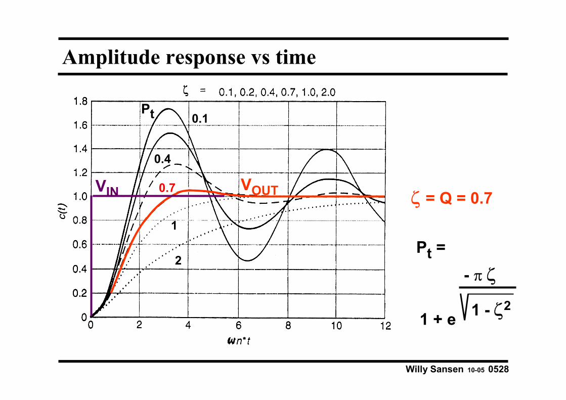
Amplitude response vs time
0.1
1
2
0.7
0.4
ζ = Q = 0.7VIN VOUT
Pt = - π ζ
1 - ζ21 + e
Pt

Willy Sansen 10-05 0529
Table of contents
• Use of operational amplifiers
• Stability of 2-stage opamp
• Pole splitting
• Compensation of positive zero
• Stability of 3-stage opamp
Willy Sansen 10-05 0530
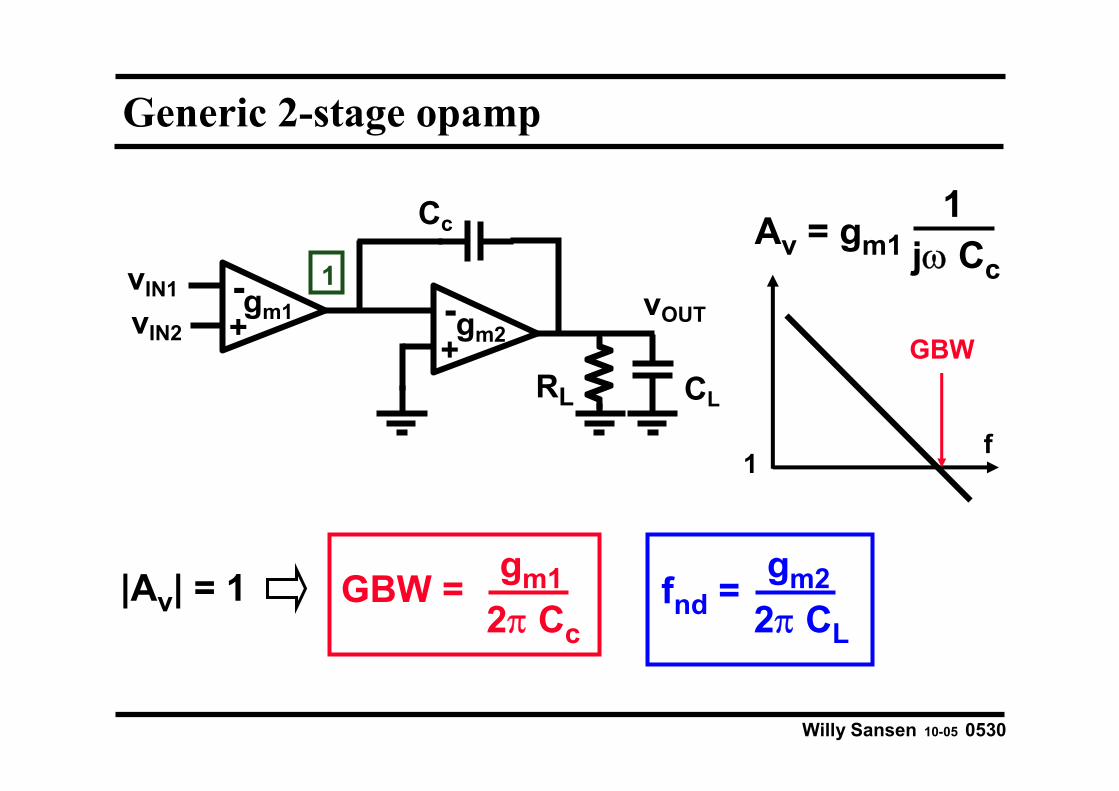
Generic 2-stage opamp
+- vOUT
RL
vIN1
vIN2
Cc
+- 1gm1 gm2
CL
Av = gm11
jω Cc
|Av| = 1 fnd =gm2
2π CLGBW = gm1
2π Cc
f1
GBW

Willy Sansen 10-05 0531
Generic 2-stage opamp
+- vOUT
RL
vIN1
vIN2
Cc
+-
Cn1
1gm1 gm2
CL
Av = gm11
jω Cc
|Av| = 1 fnd =gm2
2π CLGBW = gm1
2π Cc
1
1 +Cc
Cn1
f1
GBW

Willy Sansen 10-05 0532
Elementary design of 2-stage opamp
GBW = gm12π Cc
fnd = 3 GBW =gm2
2π CL
1
1 +Cc
Cn1
≈ 0.3
GBW = 100 MHz for CL = 2 pF
Solution: choose Cc = 1 pF
gm2gm1
≈ 4Cc
CL
Larger current in 2nd stage !

Willy Sansen 10-05 0533
Table of contents
• Use of operational amplifiers
• Stability of 2-stage opamp
• Pole splitting
• Compensation of positive zero
• Stability of 3-stage opamp

Willy Sansen 10-05 0534
Generic 2-stage opamp : Miller OTA
+- vOUT
RL
vIN1
vIN2
Cc
+-
Cn1
1gm1 gm2
CL
gm1(vIN2-vIN1)
-
+
-
+1 vOUTCc
Rn1
vn1
Cn1 gm2vn1RL CL
Av0 = - Av1Av2
Av1 = gm1Rn1
Av2 = - gm2RL

Willy Sansen 10-05 0535
Generic two-stage opamp
+- vOUT
RL
vIN1
vIN2
Cc
+-
Cn1
1gm1 gm2
CL
Av0 = - Av1Av2
Av1 = gm1Rn1
Av2 = gm2RL
Av = Av0
1 - sCcgm2
1 + (Rn1Cn1+Av2Rn1Cc+RLCL)s + Rn1RLCCs2
Rn1
CC = Cn1Cc + Cn1CL + CcCL

Willy Sansen 10-05 0536
Approximate poles and zeros
A = A0 1 - cs
1 + a s + b s2
Zero s = 1c
Pole s1 = - 1a
s2 = - if s2 >> s1ab

Willy Sansen 10-05 0537
Miller OTA : pole splitting with Cc
1k 1M Hz
1k 1M
1pF
0.1pF
Cc
|Av|10fF
1
10
100
1000
f
f
fd
fnd
fz
Av0
BW
GBW
Pole splitting
0.1
fd = 2π Av2Rn1Cc
1
fz = 2π Cc
gm2
Hz
Pole splitting for high Cc :
is a positive zero !
1pF
10fF

Willy Sansen 10-05 0538
Effect of positive zero
Av = Av0
-180o
-90o
0o
f1 f2 f
180o
φAf
1 + j f / f2
1 + j f / f1Av = Av0
1 - j f / f21 + j f / f1
-180o
-90o
0o
f1 f2 fφAf
|Av ||Av |
For phase, a positive
zerois like a negative
pole !!!
Negative zero Positive zero

Willy Sansen 10-05 0539
Miller OTA : pole splitting with gm2
1k Hz
1k 1M
10µS
gm2
|Av|0.1µS
1
10
100
1000
f
f
fd fnd fz
BW
Pole splitting
0.1
fd = 2π Av2Rn1Cc
1
fz = 2π Cc
gm2
Hz
Pole splitting for high gm2 :
is a positive zero !0.1µS
250 µS10 µS
1µS 1 µS
0.1 µS
250 µS10 µS
1µS
1M
GBW
Willy Sansen 10-05 0540
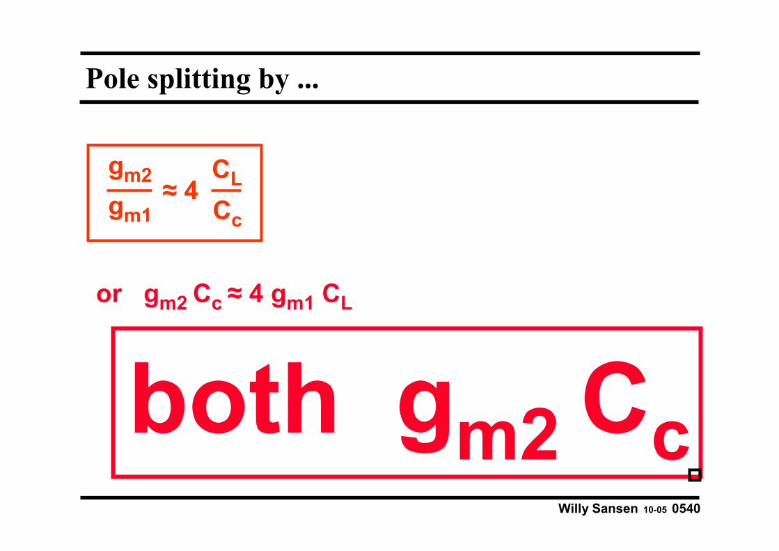
Pole splitting by ...
gm2gm1
≈ 4Cc
CL
or gm2 Cc ≈ 4 gm1 CL
both gm2 Cc
Willy Sansen 10-05 0541
Table of contents
• Use of operational amplifiers
• Stability of 2-stage opamp
• Pole splitting
• Compensation of positive zero
• Stability of 3-stage opamp

Willy Sansen 10-05 0542
Positive zero because feedforward
+-
vOUT
RL
vIN1
vIN2
Cc
+-
Cn1
gm1 gm2
CL
vOUT
RL
vIN1
vIN2
Cc
+-
Cn1
gm1
CL
Miller effectIs feedback
Feedforward
Cut !
Willy Sansen 10-05 0543
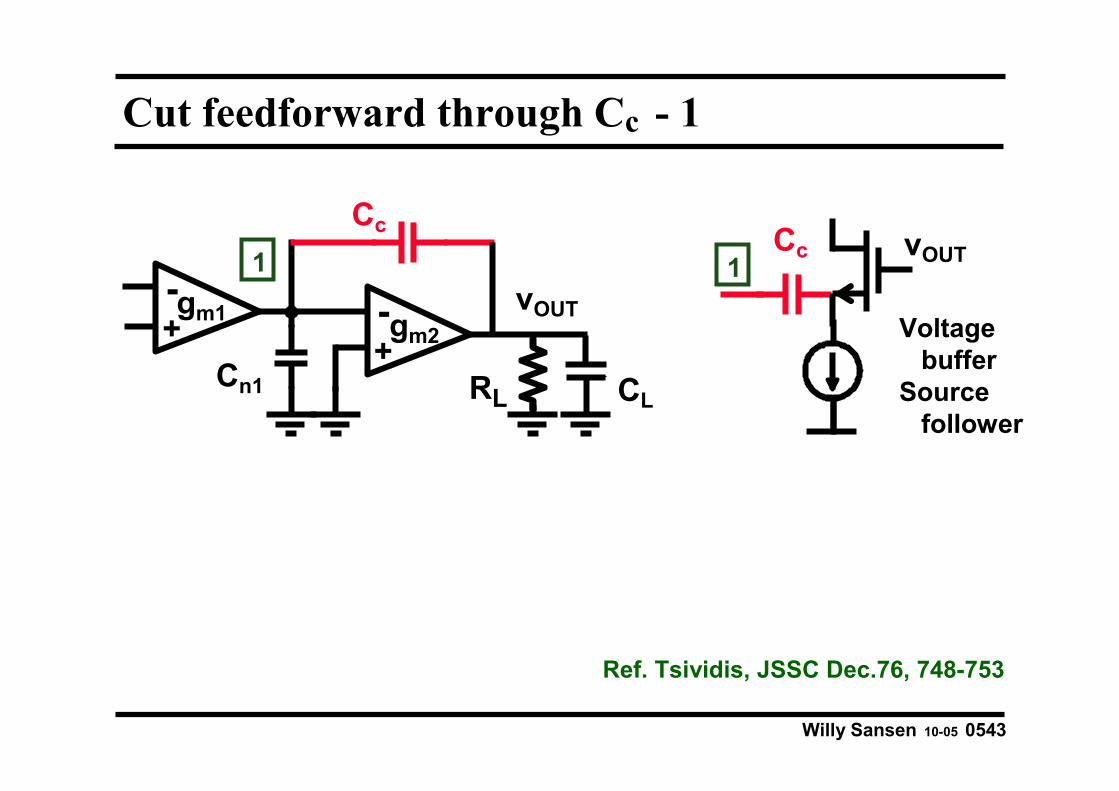
Cut feedforward through Cc - 1
+- vOUT
RL
Cc
+-
Cn1
gm1 gm2
CL
1 1vOUTCc
Voltagebuffer
Sourcefollower
Ref. Tsividis, JSSC Dec.76, 748-753
Willy Sansen 10-05 0544
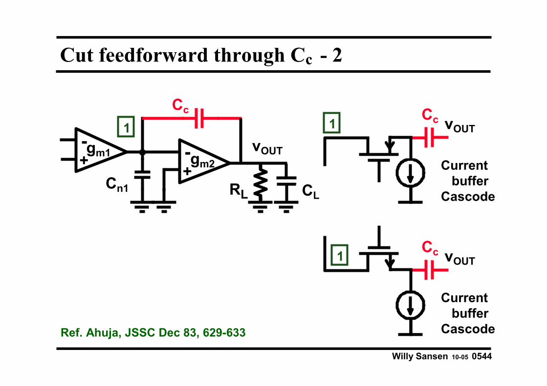
Cut feedforward through Cc - 2
+- vOUT
RL
Cc
+-
Cn1
gm1 gm2
CL
1
vOUTCc1
Currentbuffer
CascodeRef. Ahuja, JSSC Dec 83, 629-633
vOUTCc1
Currentbuffer
Cascode
Willy Sansen 10-05 0545
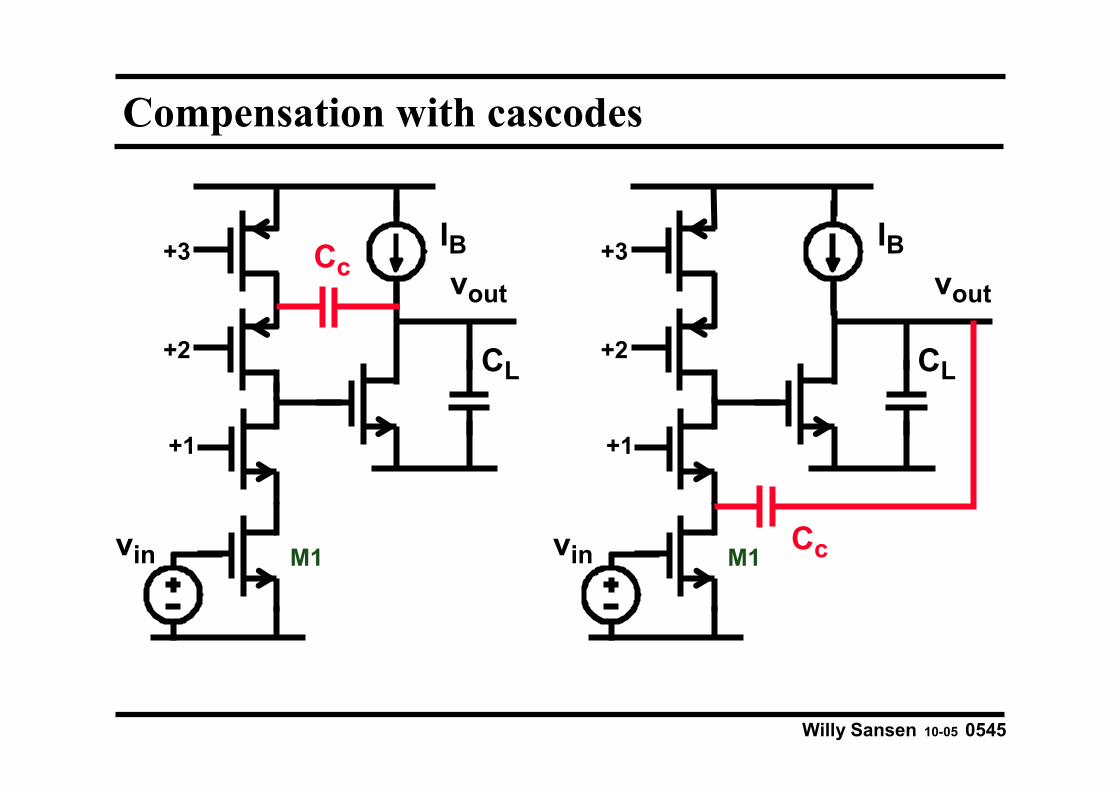
Compensation with cascodes
IB
+1
vin M1
CL+2
+3vout
CcIB
+1
vin M1
+2
+3vout
Cc
CL

Willy Sansen 10-05 0546
Cut feedforward through Cc - 3
+- vOUT
RL
Cc
+-
Cn1
gm1 gm2
CL
11 vOUT
CcRc
vOUTCc
Rc1
fz = 2π Cc (1/gm2 - Rc)
1Rc = 1/gm2 No zeroRc > 1/gm2 Negative zero
3
Ref. Senderovics, JSSC Dec 78, 760-766

Willy Sansen 10-05 0547
Negative zero compensation
fz = -2π Cc Rc
1
Rc >> 1/gm2
fz = 3 GBW Rc = 3 gm1
1
Final choice :
< Rc <1
gm2
13gm1

Willy Sansen 10-05 0548
Exercise of 2-stage opamp
GBW = 50 MHz for CL = 2 pFFind IDS1; IDS2 ; Cc and Rc !
Choose Cc = 1 pF > gm1 = 2π CcGBW = 315 µSIDS1 = 31.5 µA & 1/gm1 ≈ 3.2 kΩ
fnd = 150 MHz > gm2 = 2π CL4GBW = 8gm1 = 2520 µSIDS2 = 252 µA & 1/gm2 ≈ 400 Ω
400 Ω < Rc < 1 kΩ : Rc = 1/√2.5 ≈ 400√2.5 ≈ 640 Ω ± 60%
Willy Sansen 10-05 0549
Table of contents
• Use of operational amplifiers
• Stability of 2-stage opamp
• Pole splitting
• Compensation of positive zero
• Stability of 3-stage opamp
Willy Sansen 10-05 0550
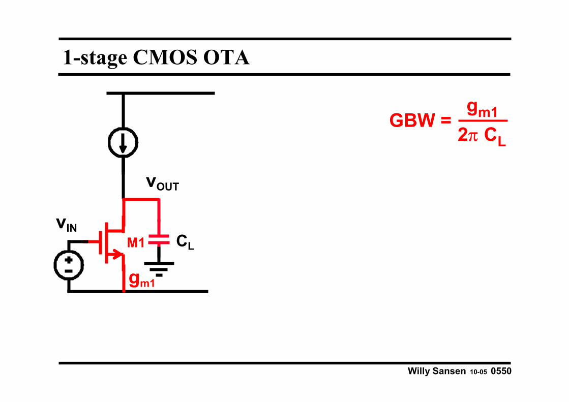
1-stage CMOS OTA
vOUT
CLM1
gm1
vIN
GBW =gm1
2π CL
Willy Sansen 10-05 0551
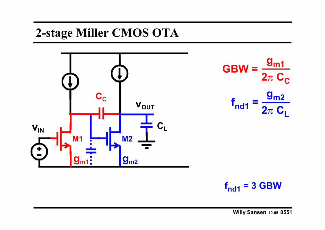
2-stage Miller CMOS OTA
vOUT
CLM2
CC
M1
gm1 gm2
vIN
GBW =gm1
2π CC
fnd1 =gm2
2π CL
fnd1 = 3 GBW
Willy Sansen 10-05 0552
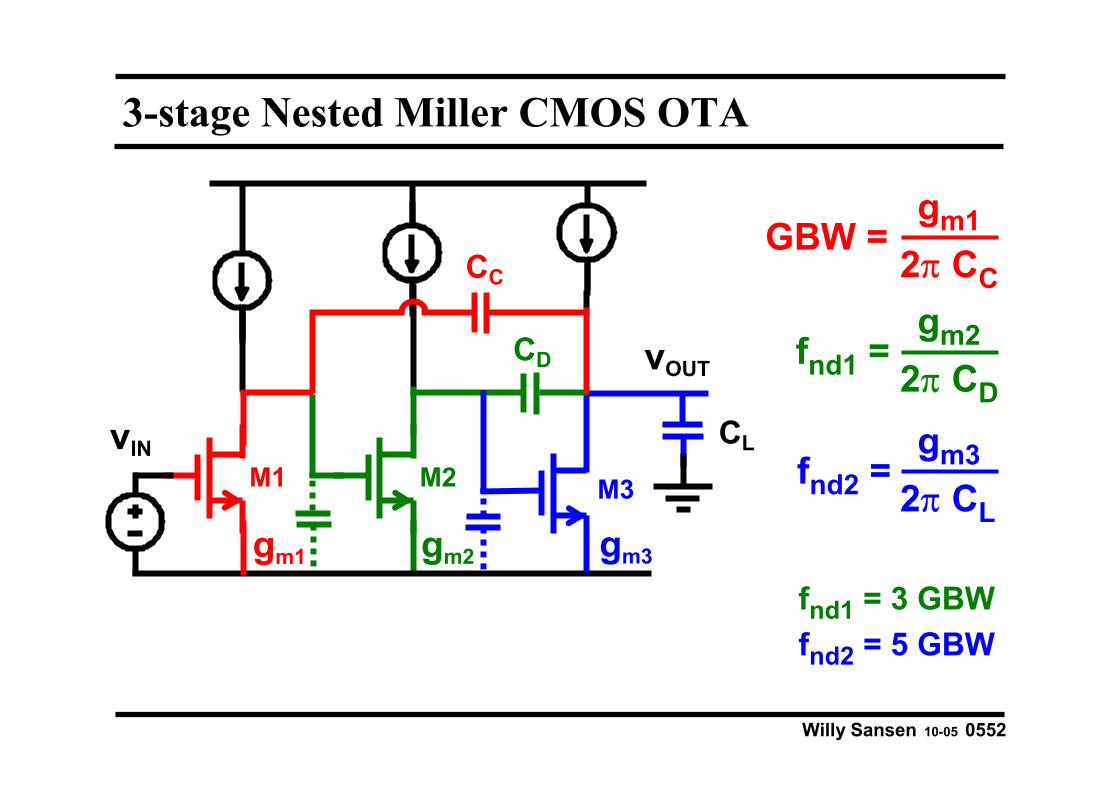
3-stage Nested Miller CMOS OTA
vOUT
CLM2 M3
CD
CC
M1
gm1 gm2 gm3
vIN
GBW =gm1
2π CC
fnd1 =gm2
2π CD
fnd2 =gm3
2π CL
fnd1 = 3 GBW fnd2 = 5 GBW

Willy Sansen 10-05 0553
Nested Miller with differential pair
Huijsing, JSSC Dec.85, pp.1144-1150
CDCC
gm1
gm2 gm3

Willy Sansen 10-05 0554
Relation between the fnd’s
10987654322
3
4
5
6
7
8
9
10
PM60
PM65
PM70
PM with two fnd's
PM = 90o
- arctan( )
- arctan( )GBWfnd2
GBWfnd1
GBWfnd1
GBWfnd2
Willy Sansen 10-05 0555
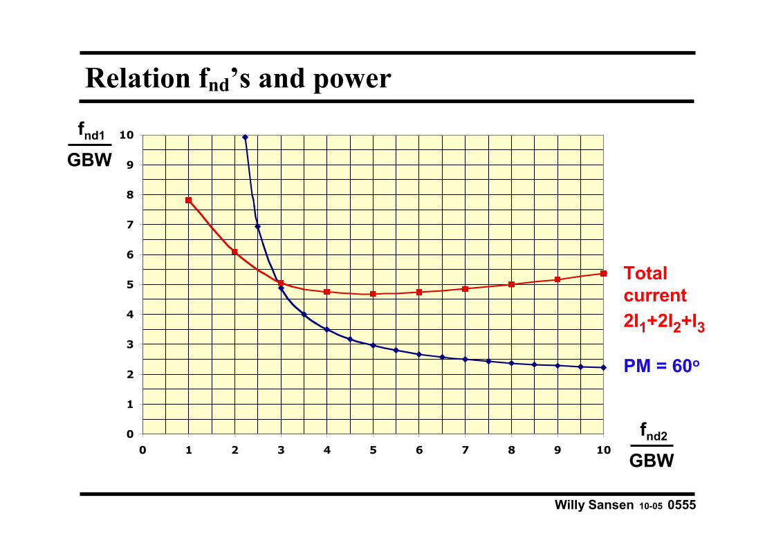
Relation fnd’s and power
0
1
2
3
4
5
6
7
8
9
10
0 1 2 3 4 5 6 7 8 9 10
GBWfnd1
GBWfnd2
PM = 60o
Totalcurrent2I1+2I2+I3

Willy Sansen 10-05 0556
Elementary design of 3-stage opamp
GBW = gm12π CC
fnd1 = 3 GBW =gm2
2π CD
gm3gm1
≈ 5CC
CL
Even larger current in output stage !
fnd2 = 5 GBW =gm3
2π CL
gm2gm1
≈ 3
Choose CD ≈ CC !

Willy Sansen 10-05 0557
Exercise of 3-stage opamp
GBW = 50 MHz for CL = 2 pFFind IDS1; IDS2 ; IDS3 ; CC and CD !
Choose CC = CD = 1 pF > gm1 = 2π CCGBW = 315 µSIDS1 = 31 µA
fnd1 = 150 MHz > gm2 = 2π CD3GBW = 3gm1 = 945 µSIDS2 = 95 µA
fnd2 = 250 MHz > gm3 = 2π CL5GBW = 10gm1 = 3150 µSIDS3 = 315 µA
Willy Sansen 10-05 0558
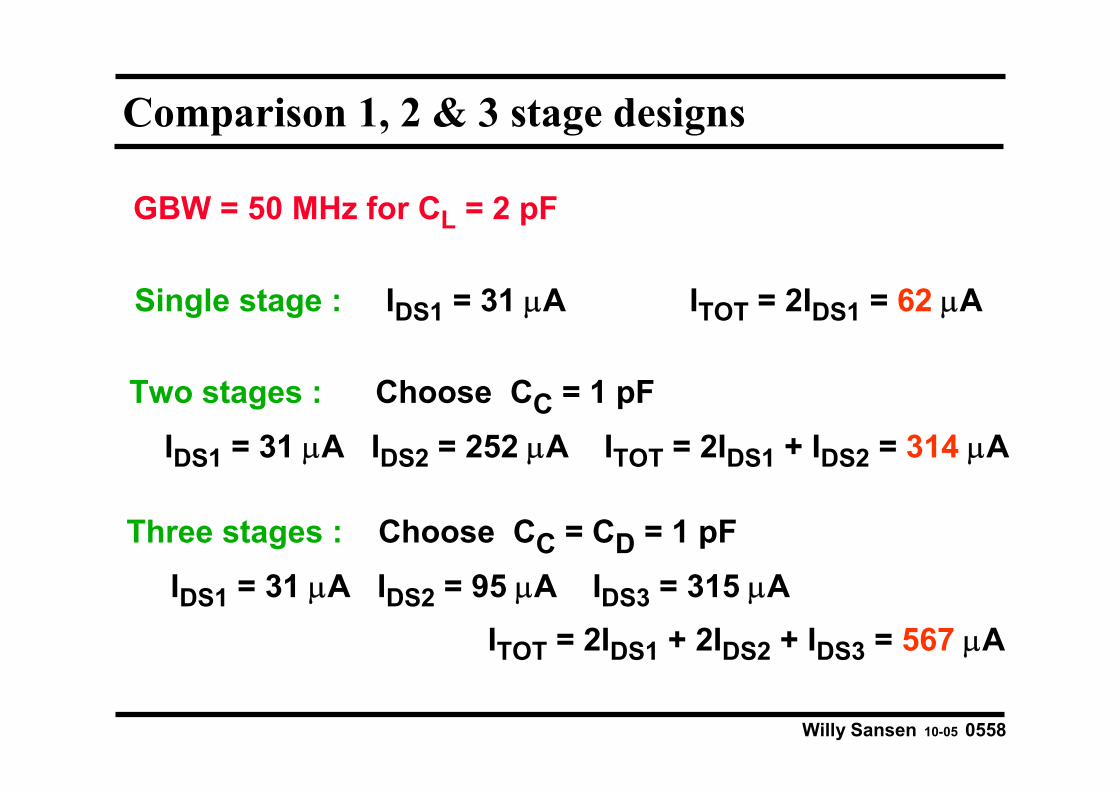
Comparison 1, 2 & 3 stage designs
GBW = 50 MHz for CL = 2 pF
Three stages : Choose CC = CD = 1 pFIDS1 = 31 µA IDS2 = 95 µA IDS3 = 315 µA
ITOT = 2IDS1 + 2IDS2 + IDS3 = 567 µA
Two stages : Choose CC = 1 pFIDS1 = 31 µA IDS2 = 252 µA ITOT = 2IDS1 + IDS2 = 314 µA
Single stage : IDS1 = 31 µA ITOT = 2IDS1 = 62 µA

Willy Sansen 10-05 0559
Table of contents
• Use of operational amplifiers
• Stability of 2-stage opamp
• Pole splitting
• Compensation of positive zero
• Stability of 3-stage opamp