st st10f269 data sheet - keil · st10f269 june 2002 high performance 40mhz cpu with dsp function ±...
TRANSCRIPT

1/160
ST10F269
June 2002
■ HIGH PERFORMANCE 40MHz CPU WITH DSPFUNCTION± 16-BIT CPU WITH 4-STAGE PIPELINE± 50ns INSTRUCTION CYCLE TIME AT 40MHz MAX
CPU CLOCK
± MULTIPLY/ACCUMULATE UNIT (MAC) 16 x 16-BITMULTIPLICATION, 40-BIT ACCUMULATOR
± REPEAT UNIT± ENHANCED BOOLEAN BIT MANIPULATION FA-
CILITIES
± ADDITIONAL INSTRUCTIONS TO SUPPORT HLLAND OPERATING SYSTEMS
± SINGLE-CYCLE CONTEXT SWITCHING SUP-PORT
■ MEMORY ORGANIZATION
± 256K BYTE ON-CHIP FLASH MEMORY SINGLEVOLTAGEWITH ERASE/PROGRAMCONTROLLER.
± 100K ERASING/PROGRAMMING CYCLES.± UP TO 16M BYTE LINEAR ADDRESS SPACE FOR
CODE AND DATA (5M BYTES WITH CAN)± 2K BYTE ON-CHIP INTERNAL RAM (IRAM)± 10K BYTE ON-CHIP EXTENSION RAM (XRAM)
■ FAST AND FLEXIBLE BUS± PROGRAMMABLE EXTERNAL BUS CHARACTE-
RISTICS FOR DIFFERENT ADDRESS RANGES± 8-BIT OR 16-BIT EXTERNAL DATA BUS
± MULTIPLEXED OR DEMULTIPLEXED EXTERNALADDRESS/DATA BUSES
± FIVE PROGRAMMABLE CHIP-SELECT SIGNALS± HOLD-ACKNOWLEDGE BUS ARBITRATION SUP-
PORT■ INTERRUPT
± 8-CHANNEL PERIPHERAL EVENT CONTROLLERFOR SINGLE CYCLE INTERRUPT DRIVEN DATATRANSFER
± 16-PRIORITY-LEVEL INTERRUPT SYSTEM WITH56 SOURCES, SAMPLING RATE DOWN TO 25ns
■ TIMERS± TWO MULTI-FUNCTIONAL GENERAL PURPOSE
TIMER UNITS WITH 5 TIMERS■ TWO 16-CHANNEL CAPTURE / COMPARE UNITS■ A/D CONVERTER
± 16-CHANNEL 10-BIT
± 4.85m s CONVERSIONTIME AT 40MHz CPU CLOCK■ 4-CHANNEL PWM UNIT■ SERIAL CHANNELS
± SYNCHRONOUS / ASYNCHRONOUS SERIALCHANNEL
± HIGH-SPEED SYNCHRONOUS CHANNEL
■ TWO CAN 2.0B INTERFACES OPERATING ON ONEOR TWO CAN BUSSES (30 OR 2x15 MESSAGEOBJECTS)
■ FAIL-SAFE PROTECTION
± PROGRAMMABLE WATCHDOG TIMER
± OSCILLATOR WATCHDOG
■ ON-CHIP BOOTSTRAP LOADER
■ CLOCK GENERATION
± ON-CHIP PLL
± DIRECT OR PRESCALEDCLOCK INPUT
■ REAL TIME CLOCK
■ UP TO 111 GENERAL PURPOSE I/O LINES
± INDIVIDUALLY PROGRAMMABLE AS INPUT,OUTPUT OR SPECIAL FUNCTION
± PROGRAMMABLE THRESHOLD (HYSTERESIS)
■ IDLE AND POWER DOWN MODES
■ SINGLE VOLTAGE SUPPLY: 5V +10% (EMBEDDEDREGULATOR FOR 3.3 V CORE SUPPLY).
■ TEMPERATURE RANGE: -40 +1255C
■ 144-PIN PQFP PACKAGE
PQFP144 (28 x 28 mm)(Plastic Quad Flat Pack)
ORDER CODE: ST10F269-Q3
CAN2_TXD
CAN1_TXDCAN1_RXD
CAN2_RXD
Port
0Po
rt1
Port
4
Port6 Port 5 Port 3
Port
2
GP
T1
ASC
usar
t
BRG
CPU-Core andMACUnit InternalRAM
Watchdog
InterruptController
8
32 16
PEC
16
16
CAN1
Port7 Port 8
Exte
rnal
Bus
10-B
itA
DC
BRG
SSC
PW
M
CAP
CO
M2
CAP
COM
116
Oscillator
Con
trolle
r
16
16
256KByte
andPLL
FlashMemory
XTAL1 XTAL2
2KByte
16 15 8 8
8
16
3.3V VoltageRegulator
10KByteXRAM
CAN2
GP
T2
16-BIT MCU WITH MAC UNIT, 256K BYTE FLASH MEMORY AND 12K BYTE RAM
PRELIMINARY DATA
This is advance information on a new product now in development or undergoing evaluation. Details are subject to change without notice.

ST10F269
2/160
TABLE OF CONTENTS PAGE
1 - INTRODUCTION .......... .......... ....... ......... ......... ........ ....... ......... .......... ..... ........... ........ . 6
2 - PIN DATA ........... ........ ....... ......... .......... ..... ......... .......... ....... ......... ......... ........ ....... ...... 7
3 - FUNCTIONAL DESCRIPTION .......... ........ ....... ........... ........ ....... ......... ......... ........ ...... 13
4 - MEMORY ORGANIZATION.......... ....... ......... ......... ...... ......... ......... ........ ....... ........... .. 14
5 - INTERNAL FLASH MEMORY .......... ........ ....... ........... ........ ....... ......... ......... ........ ...... 17
5.1 - OVERVIEW ........... ......... ........ ....... ........... ........ ....... ......... ......... ........ ....... ......... ........ . 17
5.2 - OPERATIONAL OVERVIEW ...... ......... ...... ......... .......... ....... ....... ........... ........ ....... ...... 17
5.3 - ARCHITECTURAL DESCRIPTION .......... ........ ....... ........... ........ ....... ......... ......... ...... . 19
5.3.1 - Read Mode ..... ........... ...... ......... ......... ........ ....... ......... .......... ....... ......... ......... ........ ...... 195.3.2 - Command Mode ........... ......... ........ ....... ........... ........ ..... ........... ......... ...... ......... ......... .. 195.3.3 - Ready/Busy Signal .......... ....... ......... ......... ........ ....... ......... .......... ....... ......... ......... ...... . 195.3.4 - Flash Status Register .......... .......... ....... ......... ......... ...... ......... ......... ........ ....... ........... .. 195.3.5 - Flash Protection Register ....... ......... ......... ........ ....... ........... ........ ....... ......... ......... ...... . 215.3.6 - Instructions Description .......... ....... ......... ......... ........ ....... ......... .......... ..... ........... ........ . 215.3.7 - Reset Processing and Initial State..... ........ ....... ........... ........ ....... ......... ......... ........ ...... 25
5.4 - FLASH MEMORY CONFIGURATION...... ........ ....... ......... .......... ....... ....... ........... ...... . 25
5.5 - APPLICATION EXAMPLES .......... ....... ......... ......... ...... ......... ......... ........ ....... ........... .. 25
5.5.1 - Handling of Flash Addresses ...... ......... ...... ......... .......... ....... ....... ........... ........ ....... ...... 255.5.2 - Basic Flash Access Control ...... ......... ........ ....... ........... ........ ....... ......... ......... ........ ...... 265.5.3 - Programming Examples ...... ......... ........ ....... ........... ...... ....... ........... ........ ....... ......... .... 27
5.6 - BOOTSTRAP LOADER ..... .......... ....... ......... ......... ...... ......... ......... ........ ....... ........... .. 30
5.6.1 - Entering the Bootstrap Loader ....... ......... ......... ........ ....... ........... ........ ..... ........... ........ . 305.6.2 - Memory Configuration After Reset ....... ......... ......... ...... ......... ........... ...... ....... ........... .. 315.6.3 - Loading the Startup Code ....... ......... ......... ........ ....... ........... ........ ....... ......... ......... ...... . 325.6.4 - Exiting Bootstrap Loader Mode ..... ....... ......... ......... ...... ......... ......... ........ ....... ........... .. 325.6.5 - Choosing the Baud Rate for the BSL ........ ....... ........... ........ ....... ......... ......... ........ ...... 33
6 - CENTRAL PROCESSING UNIT (CPU) .......... ........ ....... ........... ........ ....... ......... ........ . 34
6.1 - MULTIPLIER-ACCUMULATOR UNIT (MAC).......... ........... ........ ....... ......... ......... ...... . 35
6.1.1 - Features ....... ......... ......... ........ ....... ........... ........ ....... ......... ......... ........ ....... ......... ........ . 366.1.1.1 - Enhanced Addressing Capabilities..... ........ ....... ........... ........ ....... ......... ......... ........ ...... 366.1.1.2 - Multiply-Accumulate Unit...... ......... ........ ....... ........... ...... ....... ........... ........ ....... ......... .... 366.1.1.3 - Program Control ..... .......... ....... ......... ......... ........ ....... ......... .......... ....... ......... ......... ...... . 36
6.2 - INSTRUCTION SET SUMMARY.......... ..... ........... ........ ....... ......... ......... ........ ....... ...... 37
6.3 - MAC COPROCESSOR SPECIFIC INSTRUCTIONS..... ........... ........ ....... ......... ........ . 38
7 - EXTERNAL BUS CONTROLLER..... ........ ....... ........... ........ ....... ......... ......... ........ ...... 42
7.1 - PROGRAMMABLE CHIP SELECT TIMING CONTROL........... ........ ....... ......... ........ . 42
7.2 - READY PROGRAMMABLE POLARITY.......... ........ ....... ........... ........ ....... ......... ........ . 42

ST10F269
3/160
TABLE OF CONTENTS PAGE
8 - INTERRUPT SYSTEM ...... ......... .......... ..... ........... ........ ....... ......... ......... ........ ....... ...... 44
8.1 - EXTERNAL INTERRUPTS ..... ....... ......... ......... ........ ....... ......... .......... ..... ........... ........ . 44
8.2 - INTERRUPT REGISTERS AND VECTORS LOCATION LIST ........... ......... ........ ...... 45
8.3 - INTERRUPT CONTROL REGISTERS..... ........ ....... ........... ........ ....... ......... ......... ...... . 46
8.4 - EXCEPTION AND ERROR TRAPS LIST......... ....... ......... .......... ....... ......... ......... ...... . 47
9 - CAPTURE/COMPARE (CAPCOM) UNITS..... ........ ....... ........... ........ ....... ......... ........ . 48
10 - GENERAL PURPOSE TIMER UNIT...... ......... ........ ....... ........... ........ ..... ........... ........ . 51
10.1 - GPT1 ........... ........ ....... ......... .......... ....... ....... ........... ...... ......... ......... ........ ....... ......... .... 51
10.2 - GPT2 ........... ........ ....... ......... .......... ....... ....... ........... ...... ......... ......... ........ ....... ......... .... 52
11 - PWM MODULE ..... .......... ....... ......... ......... ........ ....... ......... .......... ....... ......... ......... ...... . 54
12 - PARALLEL PORTS ..... .......... ....... ......... ......... ........ ....... ......... .......... ..... ........... ........ . 55
12.1 - INTRODUCTION .......... .......... ....... ......... ......... ........ ....... ......... .......... ..... ........... ........ . 55
12.2 - I/O'S SPECIAL FEATURES .......... ....... ......... ......... ...... ......... ......... ........ ....... ........... .. 57
12.2.1 - Open Drain Mode ...... ...... ......... ......... ........ ....... ......... .......... ....... ......... ......... ........ ...... 5712.2.2 - Input Threshold Control ..... .......... ....... ......... ......... ...... ......... ......... ........ ....... ........... .. 5712.2.3 - Output Driver Control ..... ....... ......... ......... ........ ....... ......... .......... ....... ......... ......... ...... . 5812.2.4 - Alternate Port Functions ...... ......... ........ ....... ........... ...... ....... ........... ........ ....... ......... .... 60
12.3 - PORT0 ..... ........... ........ ....... ......... .......... ..... ......... .......... ....... ......... ......... ........ ....... ...... 61
12.3.1 - Alternate Functions of PORT0....... ......... ......... ........ ....... ........... ........ ..... ........... ........ . 62
12.4 - PORT1 ..... ........... ........ ....... ......... .......... ..... ......... .......... ....... ......... ......... ........ ....... ...... 64
12.4.1 - Alternate Functions of PORT1....... ......... ......... ........ ....... ........... ........ ..... ........... ........ . 64
12.5 - PORT 2 ......... ....... ......... .......... ....... ......... ......... ........ ....... ......... .......... ..... ......... .......... . 66
12.5.1 - Alternate Functions of Port 2 ...... ......... ...... ......... .......... ....... ....... ........... ........ ....... ...... 66
12.6 - PORT 3 ......... ....... ......... .......... ....... ......... ......... ........ ....... ......... .......... ..... ......... .......... . 69
12.6.1 - Alternate Functions of Port 3 ...... ......... ...... ......... .......... ....... ....... ........... ........ ....... ...... 70
12.7 - PORT 4 ......... ....... ......... .......... ....... ......... ......... ........ ....... ......... .......... ..... ......... .......... . 73
12.7.1 - Alternate Functions of Port 4 ...... ......... ...... ......... .......... ....... ....... ........... ........ ....... ...... 74
12.8 - PORT 5 ......... ....... ......... .......... ....... ......... ......... ........ ....... ......... .......... ..... ......... .......... . 77
12.8.1 - Alternate Functions of Port 5 ...... ......... ...... ......... .......... ....... ....... ........... ........ ....... ...... 7812.8.2 - Port 5 Schmitt Trigger Analog Inputs...... ......... ........ ....... ........... ........ ..... ........... ........ . 79
12.9 - PORT 6 ......... ....... ......... .......... ....... ......... ......... ........ ....... ......... .......... ..... ......... .......... . 79
12.9.1 - Alternate Functions of Port 6 ...... ......... ...... ......... .......... ....... ....... ........... ........ ....... ...... 80
12.10 - PORT 7 ......... ....... ......... .......... ....... ......... ......... ........ ....... ......... .......... ..... ......... .......... . 83
12.10.1 - Alternate Functions of Port 7 ...... ......... ...... ......... .......... ....... ....... ........... ........ ....... ...... 84
12.11 - PORT 8 ......... ....... ......... .......... ....... ......... ......... ........ ....... ......... .......... ..... ......... .......... . 87
12.11.1 - Alternate Functions of Port 8 ...... ......... ...... ......... .......... ....... ....... ........... ........ ....... ...... 88

ST10F269
4/160
TABLE OF CONTENTS PAGE
13 - A/D CONVERTER ...... ......... .......... ....... ......... ......... ...... ......... ......... ........ ....... ........... .. 90
14 - SERIAL CHANNELS .......... .......... ....... ......... ......... ...... ......... ......... ........ ....... ........... .. 91
14.1 - ASYNCHRONOUS / SYNCHRONOUS SERIAL INTERFACE (ASCO)....... ......... .... 91
14.1.1 - ASCO in Asynchronous Mode ....... ......... ......... ........ ....... ........... ........ ..... ........... ........ . 9114.1.2 - ASCO in Synchronous Mode ...... ......... ...... ......... .......... ....... ....... ........... ........ ....... ...... 93
14.2 - HIGH SPEED SYNCHRONOUS SERIAL CHANNEL (SSC) ........... ...... ......... ......... .. 95
15 - CAN MODULES ........... ......... ........ ....... ........... ........ ..... ........... ......... ...... ......... ......... .. 97
15.1 - CAN MODULES MEMORY MAPPING ..... ........... ........ ....... ......... .......... ....... ....... ...... 97
15.1.1 - CAN1 ........... ........ ....... ......... .......... ....... ....... ........... ...... ......... ......... ........ ....... ......... .... 9715.1.2 - CAN2 ........... ........ ....... ......... .......... ....... ....... ........... ...... ......... ......... ........ ....... ......... .... 97
15.2 - CAN BUS CONFIGURATIONS ..... ....... ......... ......... ...... ......... ......... ........ ....... ........... .. 97
16 - REAL TIME CLOCK ........... ......... ........ ....... ........... ...... ....... ........... ........ ....... ......... .... 99
16.1 - RTC REGISTERS ...... ......... .......... ....... ......... ......... ...... ......... ......... ........ ....... ........... .. 100
16.1.1 - RTCCON: RTC Control Register .......... ..... ........... ........ ....... ......... ......... ........ ....... ...... 10016.1.2 - RTCPH & RTCPL: RTC PRESCALER Registers......... ....... ......... .......... ....... ......... .... 10116.1.3 - RTCDH & RTCDL: RTC DIVIDER Counters .......... ...... ......... ........... ...... ......... ......... .. 10116.1.4 - RTCH & RTCL: RTC Programmable COUNTER Registers...... ........ ....... ......... ........ . 10216.1.5 - RTCAH & RTCAL: RTC ALARM Registers ..... ........ ....... ........... ........ ....... ......... ........ . 103
16.2 - PROGRAMMING THE RTC .......... ....... ......... ......... ...... ......... ......... ........ ....... ........... .. 103
17 - WATCHDOG TIMER ........... ......... ........ ....... ........... ...... ....... ........... ........ ....... ......... .... 105
18 - SYSTEM RESET .......... .......... ....... ......... ......... ........ ....... ......... .......... ..... ........... ........ . 107
18.1 - LONG HARDWARE RESET ...... ......... ...... ......... .......... ....... ....... ........... ........ ....... ...... 107
18.1.1 - Asynchronous Reset ........... ......... ........ ....... ........... ...... ....... ........... ........ ....... ......... .... 10718.1.2 - Synchronous Reset (RSTIN pulse > 1040TCL and RPD pin at high level).......... ..... . 10818.1.3 - Exit of Long Hardware Reset ...... ......... ...... ......... .......... ....... ....... ........... ........ ....... ...... 109
18.2 - SHORT HARDWARE RESET ....... ......... ......... ........ ....... ........... ........ ..... ........... ........ . 109
18.3 - SOFTWARE RESET ........... ......... ........ ....... ........... ...... ....... ........... ........ ....... ......... .... 110
18.4 - WATCHDOG TIMER RESET ..... .......... ..... ........... ........ ....... ......... ......... ........ ....... ...... 110
18.5 - RSTOUT, RSTIN, BIDIRECTIONAL RESET ......... ....... ......... .......... ..... ........... ........ . 111
18.5.1 - RSTOUT Pin .......... .......... ....... ......... ......... ........ ....... ......... .......... ....... ......... ......... ...... . 11118.5.2 - Bidirectional Reset ...... ......... .......... ....... ......... ......... ...... ......... ......... ........ ....... ........... .. 11118.5.3 - RSTIN pin ........... ........ ....... ......... .......... ..... ......... .......... ....... ......... ......... ........ ....... ...... 111
18.6 - RESET CIRCUITRY ..... .......... ....... ......... ......... ........ ....... ......... .......... ..... ........... ........ . 111
19 - POWER REDUCTION MODES ...... ......... ........ ....... ........... ........ ....... ......... ......... ...... . 114
19.1 - IDLE MODE ........... ......... ........ ....... ........... ........ ....... ......... ......... ........ ....... ......... ........ . 114
19.2 - POWER DOWN MODE .......... ....... ......... ......... ........ ....... ......... .......... ..... ........... ........ . 114
19.2.1 - Protected Power Down Mode ..... .......... ..... ........... ........ ....... ......... ......... ........ ....... ...... 11419.2.2 - Interruptable Power Down Mode .......... ..... ........... ........ ....... ......... ......... ........ ....... ...... 114

ST10F269
5/160
TABLE OF CONTENTS PAGE
20 - SPECIAL FUNCTION REGISTER OVERVIEW..... ...... ......... ........... ...... ......... ......... .. 117
20.1 - IDENTIFICATION REGISTERS ...... ......... ........ ....... ........... ........ ....... ......... ......... ...... . 123
20.2 - SYSTEM CONFIGURATION REGISTERS..... ........ ....... ........... ........ ....... ......... ........ . 124
21 - ELECTRICAL CHARACTERISTICS ........ ....... ........... ........ ....... ......... ......... ........ ...... 131
21.1 - ABSOLUTE MAXIMUM RATINGS ....... ......... ......... ...... ......... ........... ...... ....... ........... .. 131
21.2 - PARAMETER INTERPRETATION ....... ......... ......... ...... ......... ........... ...... ....... ........... .. 131
21.3 - DC CHARACTERISTICS ....... ......... ......... ........ ....... ........... ........ ....... ......... ......... ...... . 131
21.3.1 - A/D Converter Characteristics ....... ......... ......... ........ ....... ........... ........ ..... ........... ........ . 13421.3.2 - Conversion Timing Control .......... ....... ......... ......... ...... ......... ......... ........ ....... ........... .. 135
21.4 - AC CHARACTERISTICS ..... .......... ....... ......... ......... ...... ......... ......... ........ ....... ........... .. 136
21.4.1 - Test Waveforms ...... ...... ......... ......... ........ ....... ......... .......... ....... ......... ......... ........ ...... 13621.4.2 - Definition of Internal Timing ...... ......... ........ ....... ........... ........ ....... ......... ......... ........ ...... 13621.4.3 - Clock Generation Modes ..... .......... ....... ......... ......... ...... ......... ......... ........ ....... ........... .. 13721.4.4 - Prescaler Operation ........... ......... .......... ..... ........... ........ ....... ......... ......... ........ ....... ...... 13821.4.5 - Direct Drive ..... ........... ...... ......... ......... ........ ....... ......... .......... ....... ......... ......... ........ ...... 13821.4.6 - Oscillator Watchdog (OWD) .......... ....... ......... ......... ...... ......... ......... ........ ....... ........... .. 13821.4.7 - Phase Locked Loop ........... ......... .......... ..... ........... ........ ....... ......... ......... ........ ....... ...... 13821.4.8 - External Clock Drive XTAL1 .......... ....... ......... ......... ...... ......... ......... ........ ....... ........... .. 13921.4.9 - Memory Cycle Variables ...... ......... ........ ....... ........... ...... ....... ........... ........ ....... ......... .... 14021.4.10 - Multiplexed Bus ..... .......... ....... ......... ......... ........ ....... ......... .......... ....... ......... ......... ...... . 14121.4.11 - Demultiplexed Bus ...... ......... .......... ....... ......... ......... ...... ......... ......... ........ ....... ........... .. 14721.4.12 - CLKOUT and READY .......... .......... ....... ......... ......... ...... ......... ......... ........ ....... ........... .. 15321.4.13 - External Bus Arbitration .......... ....... ......... ......... ........ ....... ......... .......... ..... ........... ........ . 15521.4.14 - High-Speed Synchronous Serial Interface (SSC) Timing........... ......... .......... ....... ...... 15721.4.14.1 Master Mode........... ......... ........ ....... ........... ........ ....... ......... ......... ........ ....... ......... ........ . 15721.4.14.2 Slave mode........... ......... .......... ....... ......... ......... ........ ....... ......... .......... ..... ......... .......... . 158
22 - PACKAGE MECHANICAL DATA ..... ..... ........... ........ ....... ......... ......... ........ ....... ...... 159
23 - ORDERING INFORMATION ...... ......... ...... ......... .......... ....... ....... ........... ........ ....... ...... 159

ST10F269
6/160
1 - INTRODUCTION
The ST10F269 is a derivative of theSTMicroelectronics ST10 family of 16-bitsingle-chip CMOS microcontrollers. It combineshigh CPU performance (up to 20 millioninstructions per second) with high peripheralfunctionality and enhanced I/O-capabilities. It alsoprovides on-chip high-speed single voltage Flashmemory, on-chip high-speed RAM, and clockgeneration via PLL.
ST10F269 is processed in 0.35m m CMOStechnology. The MCU core and the logic issupplied with a 5V to 3.3V on chip voltageregulator. The part is supplied with a single 5Vsupply and I/Os work at 5V.
The device is upward compatible with theST10F168 device, with the following set ofdifferences:
± The Multiply/Accumulate unit is available asstandard. This MAC unit adds powerful DSPfunctions to the ST10 architecture, but maintainsfull compatibility for existing code.
± Flash control interface is now based onSTMicroelectronics third generation ofstand-alone Flash memories, with an embeddedErase/Program Controller. This completely
frees up the CPU during programming orerasing the Flash.
± Two dedicated pins (DC1 and DC2) on thePQFP-144 package are used for decoupling theinternally generated 3.3V core logic supply.Donot connect these two pins to 5.0V externalsupply. Instead, these pins should beconnected to a decoupling capacitor (ceramictype, value . 330 nF).
± The A/D Converter characteristics are differentfrom previous ST10 derivatives ones. Refer toSection 21.3.1 - A/D Converter Characteristics.
± The AC and DC parameters are adapted to the40MHz maximum CPU frequency. Thecharacterization is performed with CL = 50pFmax on output pins. Refer to Section 21.3 DCCharacteristics.
± In order to reduce EMC, the rise/fall time and thesink/source capability of the drivers of the I/Opads are programmable. Refer toSection 12.2 I/O's Special Features.
± The Real Time Clock functionnality is added.± The external interrupt sources can be selected
with the EXISEL register.± The reset source is identified by a dedicated
status bit in the WDTCON register.
Figure 1 : Logic Symbol
XTAL1
RSTIN
XTAL2
RSTOUT
NMI
EA
READY
ALE
RD
WR/WRL
Port 516-bit
Port 68-bit
Port 48-bit
Port 315-bit
Port 216-bit
Port 116-bit
Port 016-bit
VDD VSS
Port 78-bit
Port 88-bit
VAREF
VAGND
RPD
DC1 DC2
ST10F269

ST10F269
7/160
2 - PIN DATA
Figure 2 : Pin Configuration (top view)
P6.0/CS0P6.1/CS1P6.2/CS2P6.3/CS3P6.4/CS4
P6.5/HOLDP6.6/HLDAP6.7/BREQ
P8.0/CC16IOP8.1/CC17IOP8.2/CC18IOP8.3/CC19IOP8.4/CC20IO
P8.6/CC22IOP8.7/CC23IO
DC2VSS
P7.0/POUT0P7.1/POUT1P7.2/POUT2P7.3/POUT3
P8.5/CC21IO
RPD
P7.4/CC28I0P7.5/CC29I0P7.6/CC30I0P7.7/CC31I0
P5.0/AN0P5.1/AN1P5.2/AN2P5.3/AN3P5.4/AN4P5.5/AN5P5.6/AN6P5.7/AN7P5.8/AN8P5.9/AN9
P0H.0/AD8P0L.7/AD7P0L.6/AD6P0L.5/AD5P0L.4/AD4P0L.3/AD3P0L.2AD2P0L.A/AD1P0L.0/AD0EAALEREADYWR/WRLRDVSSVDDP4.7A23/CAN2_TxDP4.6A22/CAN1_TxDP4.5A21/CAN1_RxDP4.4A20/CAN2_RxDP4.3/A19P4.2/A18P4.1/A17P4.0/A16
VSSVDDP3.15/CLKOUTP3.13/SCLKP3.12/BHE/WRHP3.11/RXD0P3.10/TXD0P3.9/MTSRP3.8/MRSTP3.7/T2INP3.6/T3IN
VA
RE
FV
AG
ND
P5.
10/
AN
10/
T6E
UD
P5.
11/
AN
11/
T5E
UD
P5
.12
/AN
12/T
6IN
P5
.13
/AN
13/T
5IN
P5.
14/
AN
14/
T4E
UD
P5.
15/
AN
15/
T2E
UD
VS
SV
DD
P2.
0/C
C0I
OP
2.1
/CC
1IO
P2.
2/C
C2
IOP
2.3
/CC
3IO
P2.
4/C
C4
IOP
2.5
/CC
5IO
P2.
6/C
C6
IOP
2.7
/CC
7IO
VS
SD
C1
P2.
8/C
C8I
O/E
X0I
NP
2.9
/CC
9IO
/EX
1IN
P2.
10/C
C10
IOE
X2I
NP
2.11
/CC
11IO
EX
3IN
P2.
12/C
C12
IO/E
X4I
NP
2.13
/CC
13IO
/EX
5IN
P2.
14/C
C14
IO/E
X6I
NP
2.15
/CC
15IO
/EX
7IN
/T7I
NP
3.0
/T0I
NP
3.1/
T6O
UT
P3.
2/C
AP
INP
3.3/
T3O
UT
P3.
4/T3
EU
DP
3.5
/T4I
NV
SS
VD
D
VS
SN
MI
VD
D
RS
TO
UT
RS
TIN
VS
SX
TAL1
XTA
L2V
DD
P1H
.7/A
15/C
C27
IOP
1H.6
/A14
/CC
26IO
P1H
.5/A
13/C
C25
IOP
1H.4
/A12
/CC
24IO
P1H
.3/A
11P
1H.2
/A10
P1H
.1/A
9P
1H.0
/A8
VS
SV
DD
P1L
.7/A
7P
1L.6
/A6
P1L
.5/A
5P
1L.4
/A4
P1L
.3/A
3P
1L.2
/A2
P1L
.1/A
1P
1L.0
/A0
P0H
.7/A
D1
5P
0H.6
/AD
14P
0H.5
/AD
13
P0H
.4/A
D1
2P
0H.3
/AD
11P
0H.2
/AD
10
P0H
.1/A
D9
VS
SV
DD
123456789101112131415161718192021222324252627282930313233343536
37 38 39 40 41 42 43 44 45 46 47 48 49 50 51 52 53 54 55 56 57 58 59 60 61 62 63 64 65 66 67 68 69 70 71 72
108107106105104103102101100999897969594939291908988878685848382818079787776757473
144
143
142
141
140
139
138
137
136
135
134
133
132
131
130
129
128
127
126
125
124
123
122
121
120
119
118
117
116
115
114
113
112
111
110
109
ST10F269-Q3

ST10F269
8/160
Table 1 : Pin Description
Symbol Pin Type Function
P6.0 - P6.7 1 - 8 I/O 8-bit bidirectional I/O port, bit-wise programmable for input or output via directionbit. Programming an I/O pin as input forces the corresponding output driver to highimpedance state. Port 6 outputs can be configured as push-pull or open draindrivers. The following Port 6 pins have alternate functions:
1 O P6.0 CS0 Chip Select 0 Output
... ... ... ... ...
5 O P6.4 CS4 Chip Select 4 Output
6 I P6.5 HOLD External Master Hold Request Input
7 O P6.6 HLDA Hold Acknowledge Output
8 O P6.7 BREQ Bus Request Output
P8.0 - P8.7 9-16 I/O 8-bit bidirectional I/O port, bit-wise programmable for input or output via directionbit. Programming an I/O pin as input forces the corresponding output driver to highimpedance state. Port 8 outputs can be configured as push-pull or open draindrivers. The input threshold of Port 8 is selectable (TTL or special).The following Port 8 pins have alternate functions:
9 I/O P8.0 CC16IO CAPCOM2: CC16 Capture Input / Compare Output
... ... ... ... ...
16 I/O P8.7 CC23IO CAPCOM2: CC23 Capture Input / Compare Output
P7.0 - P7.7 19-26 I/O 8-bit bidirectional I/O port, bit-wise programmable for input or output via directionbit. Programming an I/O pin as input forces the corresponding output driver to highimpedance state. Port 7 outputs can be configured as push-pull or open draindrivers. The input threshold of Port 7 is selectable (TTL or special).The following Port 7 pins have alternate functions:
19 O P7.0 POUT0 PWM Channel 0 Output
... ... ... ... ...
22 O P7.3 POUT3 PWM Channel 3 Output
23 I/O P7.4 CC28IO CAPCOM2: CC28 Capture Input / Compare Output
... ... ... ... ...
26 I/O P7.7 CC31IO CAPCOM2: CC31 Capture Input / Compare Output
P5.0 - P5.9P5.10 - P5.15
27-3639-44
II
16-bit input-only port with Schmitt-Trigger characteristics. The pins of Port 5 can bethe analog input channels (up to 16) for the A/D converter, where P5.x equals ANx(Analog input channel x), or they are timer inputs:
39 I P5.10 T6EUD GPT2 Timer T6 External Up / Down Control Input
40 I P5.11 T5EUD GPT2 Timer T5 External Up / Down Control Input
41 I P5.12 T6IN GPT2 Timer T6 Count Input
42 I P5.13 T5IN GPT2 Timer T5 Count Input
43 I P5.14 T4EUD GPT1 Timer T4 External Up / Down Control Input
44 I P5.15 T2EUD GPT1 Timer T2 External Up / Down Control Input

ST10F269
9/160
P2.0 - P2.7P2.8 - P2.15
47-5457-64
I/O 16-bit bidirectional I/O port, bit-wise programmable for input or output via directionbit. Programming an I/O pin as input forces the corresponding output driver to highimpedance state. Port 2 outputs can be configured as push-pull or open draindrivers. The input threshold of Port 2 is selectable (TTL or special).The following Port 2 pins have alternate functions:
47 I/O P2.0 CC0IO CAPCOM: CC0 Capture Input / Compare Output
... ... ... ... ...
54 I/O P2.7 CC7IO CAPCOM: CC7 Capture Input / Compare Output
57 I/O P2.8 CC8IO CAPCOM: CC8 Capture Input / Compare Output
I EX0IN Fast External Interrupt 0 Input
... ... ... ... ...
64 I/O P2.15 CC15IO CAPCOM: CC15 Capture Input / Compare Output
I EX7IN Fast External Interrupt 7 Input
I T7IN CAPCOM2 Timer T7 Count Input
P3.0 - P3.5P3.6 - P3.13,
P3.15
65-70,73-80,
81
I/OI/OI/O
15-bit (P3.14 is missing) bidirectional I/O port, bit-wise programmable for input oroutput via direction bit. Programming an I/O pin as input forces the correspondingoutput driver to high impedance state. Port 3 outputs can be configured as push-pullor open drain drivers. The input threshold of Port 3 is selectable (TTL or special).The following Port 3 pins have alternate functions:
65 I P3.0 T0IN CAPCOM Timer T0 Count Input
66 O P3.1 T6OUT GPT2 Timer T6 Toggle Latch Output
67 I P3.2 CAPIN GPT2 Register CAPREL Capture Input
68 O P3.3 T3OUT GPT1 Timer T3 Toggle Latch Output
69 I P3.4 T3EUD GPT1 Timer T3 External Up / Down Control Input
70 I P3.5 T4IN GPT1 Timer T4 Input for Count / Gate / Reload / Capture
73 I P3.6 T3IN GPT1 Timer T3 Count / Gate Input
74 I P3.7 T2IN GPT1 Timer T2 Input for Count / Gate / Reload / Capture
75 I/O P3.8 MRST SSC Master-Receiver / Slave-Transmitter I/O
76 I/O P3.9 MTSR SSC Master-Transmitter / Slave-Receiver O/I
77 O P3.10 TxD0 ASC0 Clock / Data Output (Asynchronous /Synchronous)
78 I/O P3.11 RxD0 ASC0 Data Input (Asynchronous) or I/O (Synchronous)
79 O P3.12 BHE External Memory High Byte Enable Signal
WRH External Memory High Byte Write Strobe
80 I/O P3.13 SCLK SSC Master Clock Output / Slave Clock Input
81 O P3.15 CLKOUT System Clock Output (=CPU Clock)
Symbol Pin Type Function

ST10F269
10/160
P4.0 ±P4.7 85-92 I/O Port 4 is an 8-bit bidirectional I/O port. It is bit-wise programmable for input or outputvia direction bit. Programming an I/O pin as input forces the corresponding outputdriver to high impedance state. The input threshold is selectable (TTL or special).Port 4.6 & 4.7 outputs can be configured as push-pull or open drain drivers.In case of an external bus configuration, Port 4 can be used to output the segmentaddress lines:
85 O P4.0 A16 Segment Address Line
86 O P4.1 A17 Segment Address Line
87 O P4.2 A18 Segment Address Line
88 O P4.3 A19 Segment Address Line
89 O P4.4 A20 Segment Address Line
I CAN2_RxD CAN2 Receive Data Input
90 O P4.5 A21 Segment Address Line
I CAN1_RxD CAN1 Receive Data Input
91 O P4.6 A22 Segment Address Line
O CAN1_TxD CAN1 Transmit Data Output
92 O P4.7 A23 Most Significant Segment Address Line
O CAN2_TxD CAN2 Transmit Data Output
RD 95 O External Memory Read Strobe. RD is activated for every external instruction or dataread access.
WR/WRL 96 O External Memory Write Strobe. In WR-mode this pin is activated for every externaldata write access. In WRL mode this pin is activated for low Byte data writeaccesses on a 16-bit bus, and for every data write access on an 8-bit bus. SeeWRCFG in the SYSCON register for mode selection.
READY/READY
97 I Ready Input. The active level is programmable. When the Ready function isenabled, the selected inactive level at this pin, during an external memory access,will force the insertion of waitstate cycles until the pin returns to the selected activelevel.
ALE 98 O Address Latch Enable Output. In case of use of external addressing or of multi-plexed mode, this signal is the latch command of the address lines.
EA 99 I External Access Enable pin. A low level applied to this pin during and after Resetforces the ST10F269 to start the program from the external memory space. A highlevel forces the MCU to start in the internal memory space.
Symbol Pin Type Function

ST10F269
11/160
P0L.0 - P0L.7,P0H.0
P0H.1 - P0H.7
100-107,108,
111-117
I/O Two 8-bit bidirectional I/O ports P0L and P0H, bit-wise programmable for input oroutput via direction bit. Programming an I/O pin as input forces the correspondingoutput driver to high impedance state.In case of an external bus configuration, PORT0 serves as the address (A) and asthe address / data (AD) bus in multiplexed bus modes and as the data (D) bus indemultiplexed bus modes.
Demultiplexed bus modes
Data Path Width: 8-bit 16-bitP0L.0 ± P0L.7: D0 ± D7 D0 - D7P0H.0 ± P0H.7 I/O D8 - D15
Multiplexed bus modes
Data Path Width: 8-bit 16-bitP0L.0 ± P0L.7: AD0 ± AD7 AD0 - AD7P0H.0 ± P0H.7 A8 ± A15 AD8 - AD15
P1L.0 - P1L.7P1H.0 - P1H.7
118-125128-135
I/O Two 8-bit bidirectional I/O ports P1L and P1H, bit-wise programmable for input oroutput via direction bit. Programming an I/O pin as input forces the correspondingoutput driver to high impedance state. PORT1 is used as the 16-bit address bus (A)in demultiplexed bus modes and also after switching from a demultiplexed bus modeto a multiplexed bus mode.The following PORT1 pins have alternate functions:
132 I P1H.4 CC24IO CAPCOM2: CC24 Capture Input
133 I P1H.5 CC25IO CAPCOM2: CC25 Capture Input
134 I P1H.6 CC26IO CAPCOM2: CC26 Capture Input
135 I P1H.7 CC27IO CAPCOM2: CC27 Capture Input
XTAL1 138 I XTAL1 Oscillator amplifier and/or external clock input.
XTAL2 137 O XTAL2 Oscillator amplifier circuit output.
To clock the device from an external source, drive XTAL1 while leaving XTAL2unconnected. Minimum and maximum high / low and rise / fall times specified in theAC Characteristics must be observed.
RSTIN 140 I Reset Input with Schmitt-Trigger characteristics. A low level at this pin for a specifiedduration while the oscillator is running resets the ST10F269. An internal pull-upresistor permits power-on reset using only a capacitor connected to VSS. In bidirec-tional reset mode (enabled by setting bit BDRSTEN in SYSCON register), theRSTIN line is pulled low for the duration of the internal reset sequence.
RSTOUT 141 O Internal Reset Indication Output. This pin is driven to a low level during hardware,software or watchdog timer reset. RSTOUT remains low until the EINIT (end of ini-tialization) instruction is executed.
NMI 142 I Non-Maskable Interrupt Input. A high to low transition at this pin causes the CPU tovector to the NMI trap routine. If bit PWDCFG = `0' in SYSCON register, when thePWRDN (power down) instruction is executed, the NMI pin must be low in order toforce the ST10F269 to go into power down mode. If NMI is high and PWDCFG ='0',when PWRDN is executed, the part will continue to run in normal mode.If not used, pin NMI should be pulled high externally.
VAREF 37 - A/D converter reference voltage.
VAGND 38 - A/D converter reference ground.
RPD 84 - Timing pin for the return from interruptible powerdown mode and synchronous /asynchronous reset selection.
Symbol Pin Type Function

ST10F269
12/160
VDD 46, 72,82,93,109,126,
136, 144
- Digital Supply Voltage:= + 5V during normal operation and idle mode.
VSS 18,45,55,71,83,94,110,127,
139, 143
- Digital Ground.
DC1DC2
5617
--
3.3V Decoupling pin: a decoupling capacitor of . 330 nF must be connectedbetween this pin and nearest VSS pin.
Symbol Pin Type Function

ST10F269
13/160
3 - FUNCTIONAL DESCRIPTION
The architecture of the ST10F269 combinesadvantages of both RISC and CISC processorsand an advanced peripheral subsystem. The
block diagram gives an overview of the differenton-chip components and the high bandwidthinternal bus structure of the ST10F269.
Figure 3 : Block Diagram
P4.7 CAN2_TXD
P4.6 CAN1_TXDP4.5 CAN1_RXD
P4.4 CAN2_RXD
Por
t0
Por
t1
Po
rt4
Port 6 Port 5 Port 3
Por
t2
GP
T1
GP
T2
AS
Cus
art
BRG
CPU-Core and MAC UnitInternalRAM
Watchdog
Interrupt Controller
8
32 16
PEC
16
16
CAN1
Port 7 Port 8
Ext
erna
lBus
10-
Bit
AD
C
BRG
SS
C
PW
M
CA
PC
OM
2
CA
PC
OM
116
Oscillator
Con
trol
ler
16
16
256K Byte
and PLL
Flash Memory
XTAL1 XTAL2
2K Byte
16 15 8 8
8
16
3.3V VoltageRegulator
10K ByteXRAM
CAN2

ST10F269
14/160
4 - MEMORY ORGANIZATION
The memory space of the ST10F269 is configuredin a unified memory architecture. Code memory,data memory, registers and I/O ports areorganized within the same linear address space of16M Bytes. The entire memory space can beaccessed Byte wise or Word wise. Particularportions of the on-chip memory have additionallybeen made directly bit addressable.
Flash: 256K Bytes of on-chip Flash memory.
IRAM: 2K Bytes of on-chip internal RAM(dual-port) is provided as a storage for data,system stack, general purpose register banks andcode. A register bank is 16 Wordwide (R0 to R15)and / or Bytewide (RL0, RH0, 0 , RL7, RH7)general purpose registers.
XRAM: 10K Bytes of on-chip extension RAM(single port XRAM) is provided as a storage fordata, user stack and code.
The XRAM is divided into 2 areas, the first 2KBytes named XRAM1 and the second 8K Bytesnamed XRAM2, connected to the internal XBUSand are accessed like an external memory in16-bit demultiplexed bus-mode without wait stateor read/write delay (50ns access at 40MHz CPUclock). Byte and Word accesses are allowed.
The XRAM1 address range is 00'E000h- 00'E7FFh if XPEN (bit 2 of SYSCON register),and XRAM1EN (bit 2 of XPERCON register) areset. If XRAM1EN or XPEN is cleared, then anyaccess in the address range 00'E000h - 00'E7FFhwill be directed to external memory interface,using the BUSCONx register corresponding toaddress matching ADDRSELx register
The XRAM2 address range is 00'C000h- 00'DFFFh if XPEN (bit 2 of SYSCON register),and XRAM2 (bit 3 of XPERCON register are set).If bit XRAM2EN or XPEN is cleared, then anyaccess in the address range 00'C000h- 00'DFFFh will be directed to external memoryinterface, using the BUSCONx registercorresponding to address matching ADDRSELxregister.As the XRAM appears like external memory, itcannot be used as system stack or as registerbanks. The XRAM is not provided for single bitstorage and therefore is not bit addressable.
SFR/ESFR: 1024 Bytes (2 x 512 Bytes) ofaddress space is reserved for the special functionregister areas. SFRs are Wordwide registerswhich are used to control and to monitor thefunction of the different on-chip units.
CAN1: Address range 00'EF00h - 00'EFFFh isreserved for the CAN1 Module access. The CAN1is enabled by setting XPEN bit 2 of the SYSCONregister and by setting CAN1EN bit 0 of the newXPERCON register. Accesses to the CAN Moduleuse demultiplexed addresses and a 16-bit databus (Byte accesses are possible). Two wait statesgive an access time of 100ns at 40MHz CPUclock. No tri-state wait states are used.
CAN2: Address range 00'EE00h - 00'EEFFh isreserved for the CAN2 Module access. The CAN2is enabled by setting XPEN bit 2 of the SYSCONregister and by setting CAN2EN bit 1 of the newXPERCON register. Accesses to the CAN Moduleuse demultiplexed addresses and a 16-bit databus (Byte accesses are possible). Two wait statesgive an access time of 100ns at 40MHz CPUclock. No tri-state wait states are used.
In order to meet the needs of designs where morememory is required than is provided on chip, up to16M Bytes of external RAM and/or ROM can beconnected to the microcontroller.
Note If one or the two CAN modules are used,Port 4 cannot be programmed to output all8 segment address lines. Thus, only 4segment address lines can be used,reducing the external memory space to 5MBytes (1M Byte per CS line).
Visibility of XBUS Peripherals
In order to keep the ST10F269 compatible withthe ST10C167 and with the ST10F167, the XBUSperipherals can be selected to be visible and / oraccessible on the external address / data bus.CAN1EN and CAN2EN bits of XPERCON registermust be set. If these bits are cleared before theglobal enabling with XPEN-bit in SYSCONregister, the corresponding address space, portpins and interrupts are not occupied by theperipheral, thus the peripheral is not visible andnot available. Refer to Chapter 20 - SpecialFunction Register Overview.

ST10F269
15/160
Figure 4 : ST10F269 On-chip Memory Mapping
14
07
06
05
04
00'4000
01
00
00'0000
02
00'C000
00'FFFF
SFR : 512 Bytes
00'FE00
00'FDFF
IRAM : 2K Bytes
00'F600
* Bank 0L may be remapped from segment 0 to segment 1 (Bank 1L) by setting SYSCON-ROMS1 (before EINIT)
RAM, SFR and X-pheripherals aremapped into the address space.
Seg
men
t4S
egm
ent
3S
egm
ent2
Seg
men
t1S
egm
ent0
DataPageNumber
AbsoluteMemoryAddress
00'6000
00'F1FF
ESFR : 512 Bytes
00'F000
00'EFFF
CAN1 : 256 Bytes
00'EF00
00'EEFF
CAN2 : 256 Bytes
00'EE00
00'E7FF
XRAM1 : 2K Bytes
00'E000
00'DFFF
XRAM2 : 8K Bytes
00'C000
03
00'EC14
Real Time Clock
00'EC00Block2 = 8K Bytes
InternalFlashMemory
Block1 = 8K Bytes
Block0 = 16K Bytes
Bank OL
01'0000
01'8000
02'0000
03'00000C
04'000010
05'0000
Block6 = 64K Bytes
Block5 = 64K Bytes
Block4 = 64K Bytes
Block3 = 32K Bytes
Block2*Block1*Block0*
Bank 1L
Bank 1H
Data Page Number and Absolute Memory Address are hexadecimal values.
08
ST10F269
16/160
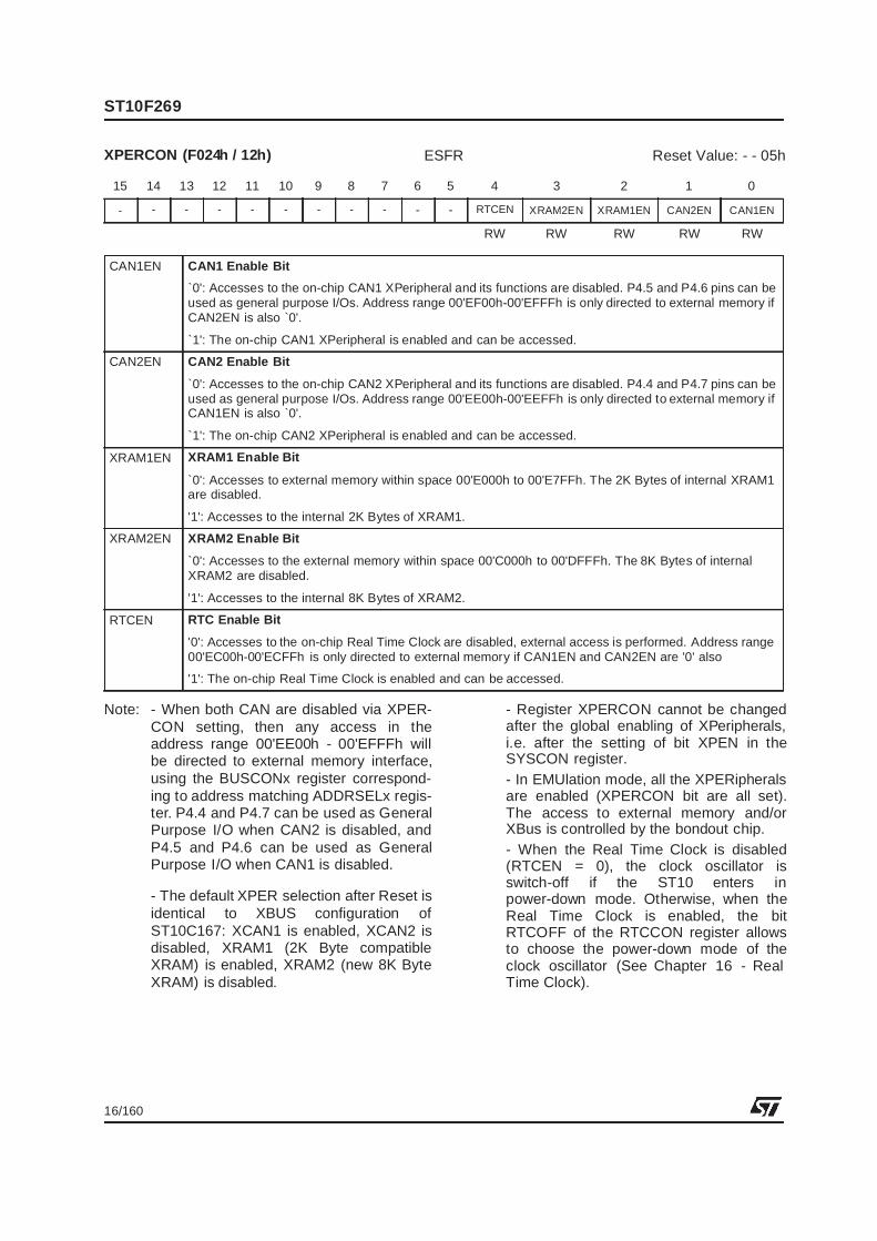
XPERCON (F024h / 12h) ESFR Reset Value: - - 05h
Note: - When both CAN are disabled via XPER-CON setting, then any access in theaddress range 00'EE00h - 00'EFFFh willbe directed to external memory interface,using the BUSCONx register correspond-ing to address matching ADDRSELx regis-ter. P4.4 and P4.7 can be used as GeneralPurpose I/O when CAN2 is disabled, andP4.5 and P4.6 can be used as GeneralPurpose I/O when CAN1 is disabled.
- The default XPER selection after Reset isidentical to XBUS configuration ofST10C167: XCAN1 is enabled, XCAN2 isdisabled, XRAM1 (2K Byte compatibleXRAM) is enabled, XRAM2 (new 8K ByteXRAM) is disabled.
- Register XPERCON cannot be changedafter the global enabling of XPeripherals,i.e. after the setting of bit XPEN in theSYSCON register.- In EMUlation mode, all the XPERipheralsare enabled (XPERCON bit are all set).The access to external memory and/orXBus is controlled by the bondout chip.- When the Real Time Clock is disabled(RTCEN = 0), the clock oscillator isswitch-off if the ST10 enters inpower-down mode. Otherwise, when theReal Time Clock is enabled, the bitRTCOFF of the RTCCON register allowsto choose the power-down mode of theclock oscillator (See Chapter 16 - RealTime Clock).
15 14 13 12 11 10 9 8 7 6 5 4 3 2 1 0
- - - - - - - - - - - RTCEN XRAM2EN XRAM1EN CAN2EN CAN1EN
RW RW RW RW RW
CAN1EN CAN1 Enable Bit
`0': Accesses to the on-chip CAN1 XPeripheral and its functions are disabled. P4.5 and P4.6 pins can beused as general purpose I/Os. Address range 00'EF00h-00'EFFFh is only directed to external memory ifCAN2EN is also `0'.
`1': The on-chip CAN1 XPeripheral is enabled and can be accessed.
CAN2EN CAN2 Enable Bit
`0': Accesses to the on-chip CAN2 XPeripheral and its functions are disabled. P4.4 and P4.7 pins can beused as general purpose I/Os. Address range 00'EE00h-00'EEFFh is only directed to external memory ifCAN1EN is also `0'.
`1': The on-chip CAN2 XPeripheral is enabled and can be accessed.
XRAM1EN XRAM1 Enable Bit
`0': Accesses to external memory within space 00'E000h to 00'E7FFh. The 2K Bytes of internal XRAM1are disabled.
'1': Accesses to the internal 2K Bytes of XRAM1.
XRAM2EN XRAM2 Enable Bit
`0': Accesses to the external memory within space 00'C000h to 00'DFFFh. The 8K Bytes of internalXRAM2 are disabled.
'1': Accesses to the internal 8K Bytes of XRAM2.
RTCEN RTC Enable Bit
'0': Accesses to the on-chip Real Time Clock are disabled, external access is performed. Address range00'EC00h-00'ECFFh is only directed to external memory if CAN1EN and CAN2EN are '0' also
'1': The on-chip Real Time Clock is enabled and can be accessed.

ST10F269
17/160
5 - INTERNAL FLASH MEMORY
5.1 - Overview
± 256K Byte on-chip Flash memory
± Two possibilities of Flash mapping into the CPUaddress space
± Flash memory can be used for code and datastorage
± 32-bit, zero waitstate read access (50ns cycletime at fCPU = 40MHz)
± Erase-Program Controller (EPC) similar toM29F400B STM's stand-alone Flash memory
ωWord-by-Word Programmable (16m s typical)
ωData polling and Toggle Protocol for EPCStatus
ωReady/Busy signal connected on XP2INTinterrupt line
ωInternal Power-On detection circuit
± Memory Erase in blocks
ωOne 16K Byte, two 8K Byte, one 32K Byte,three 64K Byte blocks
ωEach block can be erased separately(1.5 second typical)
ωChip erase (8.5 second typical)
ωEach block can be separately protectedagainst programming and erasing
ωEach protected block can be temporary unpro-tected
ωWhen enabled, the read protection preventsaccess to data in Flash memory using a pro-gram running out of the Flash memory space.
Access to data of internal Flash can only be per-formed with an inner protected program
± Erase Suspend and Resume Modes
ωRead and Program another Block during erasesuspend
± Single Voltage operation , no need of dedicatedsupply pin
± Low Power Consumption:
ω45mA max. Read current
ω60mA max. Program or Erase current
ωAutomatic Stand-by-mode (50m A maximum)
± 100,000 Erase-Program Cycles per block,20 years of data retention time
± Operating temperature: -40 to +125oC
5.2 - Operational Overview
Read Mode
In standard mode (the normal operating mode)the Flash appears like an on-chip ROM with thesame timing and functionality. The Flash moduleoffers a fast access time, allowing zero waitstateaccess with CPU frequency up to 40MHz.Instruction fetches and data operand reads areperformed with all addressing modes of theST10F269 instruction set.
In order to optimize the programming time of theinternal Flash, blocks of 8K Bytes, 16K Bytes,32K Bytes, 64K Bytes can be used. But the size ofthe blocks does not apply to the whole memoryspace, see details in Table 2.
Table 2 : 256K Byte Flash Memory Block Organisation
Block Addresses (Segment 0) Addresses (Segment 1) Size (byte)
0
1
2
3
4
5
6
00'0000h to 00'3FFFh
00'4000h to 00'5FFFh
00'6000h to 00'7FFFh
01'8000h to 01'FFFFh
02'0000h to 02'FFFFh
03'0000h to 03'FFFFh
04'0000h to 04'FFFFh
01'0000h to 01'3FFFh
01'4000h to 01'5FFFh
01'6000h to 01'7FFFh
01'8000h to 01'FFFFh
02'0000h to 02'FFFFh
03'0000h to 03'FFFFh
04'0000h to 04'FFFFh
16K
8K
8K
32K
64K
64K
64K

ST10F269
18/160
Instructions and CommandsAll operations besides normal read operations areinitiated and controlled by command sequenceswritten to the Flash Command Interface (CI). TheCommand Interface (CI) interprets words writtento the Flash memory and enables one of thefollowing operations:± Read memory array± Program Word± Block Erase± Chip Erase± Erase Suspend± Erase Resume± Block Protection± Block Temporary Unprotection± Code ProtectionCommands are composed of several write cyclesat specific addresses of the Flash memory. Thedifferent write cycles of such commandsequences offer a fail-safe feature to protectagainst an inadvertent write.A command only starts when the CommandInterface has decoded the last write cycle of anoperation. Until that last write is performed, Flashmemory remains in Read ModeNotes: 1. As it is not possible to perform write
operations in the Flash while fetching codefrom Flash, the Flash commands must bewritten by instructions executed frominternal RAM or external memory.
2. Command write cycles do not need tobe consecutively received, pauses areallowed, save for Block Erase command.During this operation all Erase Confirmcommands must be sent to complete anyblock erase operation before time-outperiod expires (typically 96m s). Commandsequencing must be followed exactly. Anyinvalid combination of commands will resetthe Command Interface to Read Mode.
Status RegisterThis register is used to flag the status of thememory and the result of an operation. Thisregister can be accessed by read cycles duringthe Erase-Program Controller (EPC) operation.
Erase OperationThis Flash memory features a block erasearchitecture with a chip erase capability too. Eraseis accomplished by executing the six cycle erasecommand sequence. Additional command writecycles can then be performed to erase more than
one block in parallel. When a time-out periodelaps (96m s) after the last cycle, theErase-Program Controller (EPC) automaticallystarts and times the erase pulse and executes theerase operation. There is no need to program theblock to be erased with `0000h' before an eraseoperation. Termination of operation is indicated inthe Flash status register. After erase operation,the Flash memory locations are read as 'FFFFh'value.
Erase Suspend
A block erase operation is typically executedwithin 1.5 second for a 64K Byte block. Erasure ofa memory block may be suspended, in order toread data from another block or to program data inanother block, and then resumed.
In-System Programming
In-system programming is fully supported. Nospecial programming voltage is required. Becauseof the automatic execution of erase andprogramming algorithms, write operations arereduced to transferring commands and data to theFlash and reading the status. Any code thatprograms or erases Flash memory locations (thatwrites data to the Flash) must be executed frommemory outside the on-chip Flash memory itself(on-chip RAM or external memory).
A boot mechanism is provided to supportin-system programming. It works using serial linkvia USART interface and a PC compatible or otherprogramming host.
Read/Write Protection
The Flash module supports read and writeprotection in a very comfortable and advancedprotection functionality. If Read Protection isinstalled, the whole Flash memory is protectedagainst any ºexternalº read access; readaccesses are only possible with instructionsfetched directly from program Flash memory. Forupdate of the Flash memory a temporary disableof Flash Read Protection is supported.
The device also features a block write protection.Software locking of selectable memory blocks isprovided to protect code and data. This featurewill disable both program and erase operations inthe selected block(s) of the memory. BlockProtection is accomplished by block specificlock-bit which are programmed by executing afour cycle command sequence. The locked stateof blocks is indicated by specific flags in theaccording block status registers. A block may onlybe temporarily unlocked for update (write)operations.

ST10F269
19/160
With the two possibilities for write protection -whole memory or block specific - a flexibleinstallation of write protection is supported toprotect the Flash memory or parts of it fromunauthorized programming or erase accessesand to provide virus-proof protection for all systemcode blocks. All write protection also is enabledduring boot operation.
Power Supply, ResetThe Flash module uses a single power supply forboth read and write functions. Internally generatedand regulated voltages are provided for theprogram and erase operations from 5V supply.Once a program or erase cycle has beencompleted, the device resets to the standard readmode. At power-on, the Flash memory has a setupphase of some microseconds (dependent on thepower supply ramp-up). During this phase, Flashcan not be read. Thus, ifEA pin is high (executionwill start from Flash memory), the CPU will remainsin reset state until the Flash can be accessed.
5.3 - Architectural DescriptionThe Flash module distinguishes two basicoperating modes, the standard read mode and thecommand mode. The initial state after power-onand after reset is the standard read mode.
5.3.1 - Read ModeThe Flash module enters the standard operatingmode, the read mode:± After Reset command± After every completed erase operation± After every completed programming operation± After every other completed command
execution± Few microseconds after a CPU-reset has
started± After incorrect address and data values of
command sequences or writing them in animproper sequence
± After incorrect write access to a read protectedFlash memory
The read mode remains active until the lastcommand of a command sequence is decodedwhich starts directly a Flash array operation, suchas:± erase one or several blocks± program a word into Flash array± protect / temporary unprotect a block.In the standard read mode read accesses aredirectly controlled by the Flash memory array,delivering a 32-bit double Word from the
addressed position. Read accesses are alwaysaligned to double Word boundaries. Thus, bothlow order address bit A1 and A0 are not used inthe Flash array for read accesses. The high orderaddress bit A17/A16 define the physical 64K Bytesegment being accessed within the Flash array.
5.3.2 - Command Mode
Every operation besides standard read operationsis initiated by commands written to the Flashcommand register. The addresses used forcommand cycles define in conjunction with theactual state the specific step within commandsequences. With the last command of a commandsequence, the Erase-Program Controller (EPC)starts the execution of the command. The EPCstatus is indicated during command execution by:
± The Status Register,
± The Ready/Busy signal.
5.3.3 - Ready/Busy Signal
The Ready/Busy (R/B) signal is connected to theXPER2 interrupt node (XP2IC). WhenR/B is high,the Flash is busy with a Program or Eraseoperation and will not accept any additionalprogram or erase instruction. When R/B is Low,the Flash is ready for any Read/Write or Eraseoperation. The R/B will also be low when thememory is put in Erase Suspend mode.
This signal can be polled by reading XP2ICregister, or can be used to trigger an interruptwhen the Flash goes from Busy to Ready.
5.3.4 - Flash Status Register
The Flash Status register is used to flag the statusof the Flash memory and the result of anoperation. This register can be accessed by Readcycles during the program-Erase Controlleroperations. The program or erase operation canbe controlled by data polling on bit FSB.7 ofStatus Register, detection of Toggle on FSB.6 andFSB.2, or Error on FSB.5 and Erase Timeout onFSB.3 bit. Any read attempt in Flash during EPCoperation will automatically output these five bits.The EPC sets bit FSB.2, FSB.3, FSB.5, FSB.6and FSB.7. Other bits are reserved for future useand should be masked.

ST10F269
20/160
Flash Status (see note for address)
Note: The Address of Flash Status Register is the address of the word being programmed whenProgramming operation is in progress, or an address within block being erased when Erasingoperation is in progress.
15 14 13 12 11 10 9 8 7 6 5 4 3 2 1 0
- - - - - - - - FSB.7 FSB.6 FSB.5 - FSB.3 FSB.2 - -
R R R R R
FSB.7 Flash Status bit 7: Data Polling BitProgramming Operation: this bit outputs the complement of the bit 7 of the word beingprogrammed, and after completion, will output the bit 7 of the word programmed.Erasing Operation: outputs a `0' during erasing, and `1' after erasing completion.If the block selected for erasure is (are) protected, FSB.7 will be set to `0' for about 100 m s, andthen return to the previous addressed memory data value.FSB.7 will also flag the Erase Suspend Mode by switching from `0' to `1' at the start of theErase Suspend.During Program operation in Erase Suspend Mode, FSB.7 will have the same behaviour as innormal Program execution outside the Suspend mode.
FSB.6 Flash Status bit 6: Toggle BitProgramming or Erasing Operations: successive read operations of Flash Status register willdeliver complementary values. FSB.6 will toggle each time the Flash Status register is read.The Program operation is completed when two successive reads yield the same value. Thenext read will output the bit last programmed, or a `1' after Erase operationFSB.6 will be set to`1' if a read operation is attempted on an Erase Suspended block. Inaddition, an Erase Suspend/Resume command will cause FSB.6 to toggle.
FSB.5 Flash Status bit 5: Error BitThis bit is set to `1' when there is a failure of Program, block or chip erase operations.This bitwill also be set if a user tries to program a bit to `1' to a Flash location that is currentlyprogrammed with `0'.The error bit resets after Read/Reset instruction.In case of success, the Error bit will be set to `0' during Program or Erase and then will outputthe bit last programmed or a `1' after erasing
FSB.3 Flash Status bit 3: Erase Time-out BitThis bit is cleared by the EPC when the last Block Erase command has been entered to theCommand Interface and it is awaiting the Erase start. When the time-out period is finished,after 96 m s, FSB.3 returns back to `1'.
FSB.2 Flash Status bit 2: Toggle BitThis toggle bit, together with FSB.6, can be used to determine the chip status during the EraseMode or Erase Suspend Mode. It can be used also to identify the block being ErasedSuspended. A Read operation will cause FSB.2 to Toggle during the Erase Mode. If the Flashis in Erase Suspend Mode, a Read operation from the Erase suspended block or a Programoperation into the Erase suspended block will cause FSB.2 to toggle.When the Flash is in Program Mode during Erase Suspend, FSB.2 will be read as `1' if addressused is the address of the word being programmed.After Erase completion with an Error status, FSB.2 will toggle when reading the faulty sector.

ST10F269
21/160
5.3.5 - Flash Protection Register
The Flash Protection register is a non-volatile register that contains the protection status. This registercan be read by using the Read Protection Status (RP) command, and programmed by using the dedi-cated Set Protection command.
Flash Protection Register (PR)
5.3.6 - Instructions DescriptionTwelve instructions dedicated to Flash memoryaccesses are defined as follow:Read/Reset (RD). The Read/Reset instructionconsist of one write cycle with data XXF0h . it canbe optionally preceded by two CI enable codedcycles (data xxA8h at address 1554h + dataxx54h at address 2AA8h). Any successive readcycle following a Read/Reset instruction will readthe memory array. A Wait cycle of 10m s isnecessary after a Read/Reset command if thememory was in program or Erase mode.Program Word (PW). This instruction uses fourwrite cycles. After the two Cl enable coded cycles,the Program Word command xxA0h is written ataddress 1554h. The following write cycle will latchthe address and data of the word to beprogrammed. Memory programming can be doneonly by writing 0's instead of 1's, otherwise anerror occurs. During programming, the FlashStatus is checked by reading the Flash Status bitFSB.2, FSB.5, FSB.6 and FSB.7 which show thestatus of the EPC. FSB.2, FSB.6 and FSB.7determine if programming is on going or has
completed, and FSB.5 allows a check to be madefor any possible error.
Block Erase (BE). This instruction uses aminimum of six command cycles. The eraseenable command xx80h is written at address1554h after the two-cycle CI enable sequence.
The erase confirm code xx30h must be written atan address related to the block to be erasedpreceded by the execution of a second CI enablesequence. Additional erase confirm codes mustbe given to erase more than one block in parallel.Additional erase confirm commands must bewritten within a defined time-out period. The inputof a new Block Erase command will restart thetime-out period.
When this time-out period has elapsed, the erasestarts. The status of the internal timer can bemonitored through the level of FSB.3, if FSB.3 is`0', the Block Erase command has been given andthe timeout is running; if FSB.3 is `1', the timeouthas expired and the EPC is erasing the block(s).
15 14 13 12 11 10 9 8 7 6 5 4 3 2 1 0
CP - - - - - - - - BP6 BP5 BP4 BP3 BP2 BP1 BP0
BPx Block x Protection Bit (x = 0...6)
`0': the Block Protection is enabled for block x. Programming or erasing the block is notpossible, unless a Block Temporary Unprotection command is issued.
1': the Block Protection is disabled for block x.
Bit is `1' by default, and can be programmed permanently to `0' using the Set Protectioncommand but then cannot be set to `1' again. It is therefore possible to temporally disable theBlock Protection using the Block Temporary Unprotection instruction.
CP Code Protection Bit
`0': the Flash Code Protection is enabled. Read accesses to the Flash for execution notperformed in the Flash itself are not allowed, the returned value will be 009Bh, whatever thecontent of the Flash is.
1': the Flash Code Protection is disabled: read accesses to the Flash from external or internalRAM are allowed
Bit is `1' by default, and can be programmed permanently to `0' using the Set Protectioncommand but then cannot be set to `1' again. It is therefore possible to temporally disable theCode Protection using the Code Temporary Unprotection instruction.

ST10F269
22/160
If the second command given is not an eraseconfirm or if the coded cycles are wrong, theinstruction aborts, and the device is reset to ReadMode. It is not necessary to program the block with0000h as the EPC will do this automatically beforethe erasing to FFFFh. Read operations after theEPC has started, output the Flash Status Register.
During the execution of the erase by the EPC, thedevice accepts only the Erase Suspend andRead/Reset instructions. Data Polling bit FSB.7returns `0' while the erasure is in progress, and `1'when it has completed. The Toggle bit FSB.2 andFSB.6 toggle during the erase operation. Theystop when erase is completed. After completion,the Error bit FSB.5 returns `1' if there has been anerase failure because erasure has not completedeven after the maximum number of erase cycleshave been executed by the EPC, in this case, itwill be necessary to input a Read/Reset to theCommand Interface in order to reset the EPC.
Chip Erase (CE) . This instruction uses six writecycles. The Erase Enable command xx80h, mustbe written at address 1554h after CI-Enablecycles. The Chip Erase command xx10h must begiven on the sixth cycle after a second CI-Enablesequence. An error in command sequence willreset the CI to Read mode. It is NOT necessary toprogram the block with 0000h as the EPC will dothis automatically before the erasing to FFFFh.Read operations after the EPC has started outputthe Flash Status Register. During the execution ofthe erase by the EPC, Data Polling bit FSB.7returns `0' while the erasure is in progress, and `1'when it has completed. The FSB.2 and FSB.6 bittoggle during the erase operation. They stop whenerase is finished. The FSB.5 error bit returns º1º incase of failure of the erase operation. The errorflag is set after the maximum number of erasecycles have been executed by the EPC. In thiscase, it will be necessary to input a Read/Reset tothe Command Interface in order to reset the EPC.
Erase Suspend (ES). This instruction can beused to suspend a Block Erase operation bygiving the command xxB0h without any specificaddress. No CI-Enable cycles is required. EraseSuspend operation allows reading of data fromanother block and/or the programming in anotherblock while erase is in progress. If this commandis given during the time-out period, it will terminatethe time-out period in addition to erase Suspend.The Toggle bit FSB.6, when monitored at anaddress that belongs to the block being erased,stops toggling when Erase Suspend Command iseffective, It happens between 0.1m s and 15m safter the Erase Suspend Command has been
written. The Flash will then go in normal ReadMode, and read from blocks not being erased isvalid, while read from block being erased willoutput FSB.2 toggling. During a Suspend phasethe only instructions valid are Erase Resume andProgram Word. A Read / Reset instruction duringErase suspend will definitely abort the Erase andresult in invalid data in the block being erased.
Erase Resume (ER). This instruction can begiven when the memory is in Erase SuspendState. Erase can be resumed by writing thecommand xx30h at any address without anyCl-enable sequence.
Program during Erase Suspend. The ProgramWord instruction during Erase Suspend is allowedonly on blocks that are not Erase-suspended. Thisinstruction is the same than the Program Wordinstruction.
Set Protection (SP). This instruction can be usedto enable both Block Protection (to protect eachblock independently from accidental Erasing-Pro-gramming Operation) and Code Protection (toavoid code dump). The Set Protection Commandmust be given after a special CI-Protection Enablecycles (see instruction table). The following Writecycle, will program the Protection Register. To pro-tect the block x (x = 0 to 6), the data bit x must beat `0'. To protect the code, bit 15 of the data mustbe `0'. Enabling Block or Code Protection isper-manent and can be cleared only by STM. BlockTemporary Unprotection and Code TemporaryUnprotection instructions are available to allow thecustomer to update the code.
Notes: 1. The new value programmed in protectionregister will only become active after a reset.
2. Bit that are already at '0' in protectionregister must be confirmed at '0' also indata latched during the 4th cycle of setprotection command, otherwise an errormay occur.
Read Protection Status (RP). This instruction isused to read the Block Protection status and theCode Protection status. To read the protectionregister (see Table 3), the CI-Protection Enablecycles must be executed followed by thecommand xx90h at address x2A54h. Thefollowing Read Cycles at any odd word addresswill output the Block Protection Status. The Read/Reset command xxF0h must be written to resetthe protection interface.
Note: After a modification of protection register(using Set Protection command), the ReadProtection Status will return the new PRvalue only after a reset.

ST10F269
23/160
Block Temporary Unprotection (BTU). This Instruction can be used to temporary unprotect all theblocks from Program / Erase protection. The Unprotection is disabled after a Reset cycle. The BlockTemporary Unprotection command xxC1h must be given to enable Block Temporary Unprotection. TheCommand must be preceded by the CI-Protection Enable cycles and followed by the Read/Resetcommand xxF0h.
Set Code Protection (SCP). This kind of protection allows the customer to protect the proprietary codewritten in Flash. If installed and active, Flash Code Protection prevents data operand accesses andprogram branches into the on-chip Flash area from any location outside the Flash memory itself. Dataoperand accesses and branches to Flash locations are only and exclusively allowed for instructionsexecuted from the Flash memory itself. Every read or jump to Flash performed from another memory (likeinternal RAM, external memory) while Code Protection is enabled, will give the opcode 009Bh related toTRAP #00 illegal instruction. The CI-Protection Enable cycles must be sent to set the Code Protection. Bywriting data 7FFFh at any odd word address, the Code Protected status is stored in the Flash ProtectionRegister (PR). Protection is permanent and cannot be cleared by the user. It is possible to temporarilydisable the Code Protection using Code Temporary Unprotection instruction.
Note: Bits that are already at '0' in protection register must be confirmed at '0' also in data latched duringthe 4th cycle of set protection command, otherwise an error may occur.
Code Temporary Unprotection (CTU). This instruction must be used to temporary disable CodeProtection. This instruction is effective only if executed from Flash memory space. To restore theprotection status, without using a reset, it is necessary to use a Code Temporary Protection instruction.System reset will reset also the Code Temporary Unprotected status. The Code Temporary Unprotectioncommand consists of the following write cycle:
MOV MEM, Rn ; This instruction MUST be executed from Flashmemory space
Where MEM is an absolute address inside memory space, Rn is a register loaded with data 0FFFFh.Code Temporary Protection (CTP). This instruction allows to restore Code Protection. This operation iseffective only if executed from Flash memory and is necessary to restore the protection status after theuse of a Code Temporary Unprotection instruction.The Code Temporary Protection command consists of the following write cycle:
MOV MEM, Rn ; This instruction MUST be executed from Flashmemory space
Where MEM is an absolute address inside memory space, Rn is a register loaded with data 0FFFBh.Note that Code Temporary Unprotection instruction must be used when it is necessary to modify theFlash with protected code (SCP), since the write/erase routines must be executed from a memoryexternal to Flash space. Usually, the write/erase routines, executed in RAM, ends with a return to Flashspace where a CTP instruction restore the protection.

ST10F269
24/160
Table 3 : Instructions
Notes 1. Address bit A14, A15 and above are don't care for coded address inputs.
2. X = Don't Care.
3. WA = Write Address: address of memory location to be programmed.
4. WD = Write Data: 16-bit data to be programmed
5. Optional, additional blocks addresses must be entered within a time-out delay (96 m s) after last write entry, timeout status can beverified through FSB.3 value. When full command is entered, read Data Polling or Toggle bit until Erase is completed or suspende d.
6. Read Data Polling or Toggle bit until Erase completes.
7. WPR = Write protection register. To protect code, bit 15 of WPR must be `0'. To protect block N (N=0,1,...) , bit N of WPR must be`0'. Bit that are already at `0' in protection register must also be `0' in WPR, else a writ ing error will occurs (it is not possible to write a`1' in a bit already programmed at `0').
8. MEM = any address inside the Flash memory space. Absolute addressing mode must be used (MOV MEM, Rn), and instructionmust be executed from Flash memory space.
9. Odd word address = 4n-2 where n = 0, 1, 2, 3..., ex. 0002h, 0006h...
Instruction Mne Cycle 1st
Cycle2nd
Cycle3rd
Cycle 4th Cycle 5th
Cycle6th
Cycle7th
Cycle
Read/Reset RD 1+Addr.1 X 2
Read Memory Array until a new write cycle is initiatedData xxF0h
Read/Reset RD 3+Addr.1 x1554h x2AA8h xxxxxh Read Memory Array until a new write
cycle is initiatedData xxA8h xx54h xxF0h
Program Word PW 4Addr.1 x1554h x2AA8h x1554h WA 3 Read Data Polling or Tog-
gle bit until Program com-pletes.Data xxA8h xx54h xxA0h WD 4
Block Erase BE 6Addr.1 x1554h x2AA8h x1554h x1554h x2AA8h BA BA' 5
Data xxA8h xx54h xx80h xxA8h xx54h xx30h xx30h
Chip Erase CE 6Addr.1 x1554h x2AA8h x1554h x1554h x2AA8h x1554h
Note 6
Data xxA8h xx54h xx80h xxA8h xx54h xx10h
Erase Suspend ES 1Addr.1 X2
Read until Toggle stops, then read or program all data neededfrom block(s) not being erased then Resume Erase.Data xxB0h
Erase Resume ER 1Addr.1 X2 Read Data Polling or Toggle bit until Erase completes or Erase is
supended another time.Data xx30h
Set Block/CodeProtection
SP 4
Addr.1 x2A54h x15A8h x2A54h Any oddword
address 9
Data xxA8h xx54h xxC0h WPR 7
ReadProtectionStatus RP 4
Addr.1 x2A54h x15A8h x2A54h Any oddword
address 9Read Protection Registeruntil a new write cycle isinitiated.
Data xxA8h xx54h xx90h Read PR
BlockTemporaryUnprotection
BTU 4Addr.1 x2A54h x15A8h x2A54h X2
Data xxA8h xx54h xxC1h xxF0h
CodeTemporaryUnprotection
CTU 1Addr.1 MEM 8
Write cycles must be executed from Flash.Data FFFFh
CodeTemporaryProtection
CTP 1Addr.1 MEM 8
Write cycles must be executed from Flash.Data FFFBh

ST10F269
25/160
± Generally, command sequences cannot bewritten to Flash by instructions fetched from theFlash itself. Thus, the Flash commands must bewritten by instructions, executed from internalRAM or external memory.
± Command cycles on the CPU interface need notto be consecutively received (pauses allowed).The CPU interface delivers dummy read data fornot used cycles within command sequences.
± All addresses of command cycles shall bedefined only with Register-indirect addressingmode in the according move instructions. Directaddressing is not allowed for commandsequences. Address segment or data pagepointer are taken into account for the commandaddress value.
5.3.7 - Reset Processing and Initial StateThe Flash module distinguishes two kinds of CPUreset types
The lengthening of CPU reset:± Is not reported to external devices by
bidirectional pin
± Is not enabled in case of external start of CPUafter reset.
5.4 - Flash Memory ConfigurationThe default memory configuration of theST10F269 Memory is determined by the state ofthe EA pin at reset. This value is stored in theInternal ROM Enable bit (named ROMEN) of theSYSCON register.
When ROMEN = 0, the internal Flash is disabledand external ROM is used for startup control.Flash memory can later be enabled by setting theROMEN bit of SYSCON to 1. The codeperforming this setting must not run from asegment of the external ROM to be replaced by asegment of the Flash memory, otherwiseunexpected behaviour may occur.For example, if external ROM code is located inthe first 32K Bytes of segment 0, the first32K Bytes of the Flash must then be enabled insegment 1. This is done by setting the ROMS1 bitof SYSCON to 0 before or simultaneously withsetting of ROMEN bit. This must be done in theexternally supplied program before the executionof the EINIT instruction.
If program execution starts from external memory,but access to the Flash memory mapped insegment 0 is later required, then the code thatperforms the setting of ROMEN bit must beexecuted either in the segment 0 but aboveaddress 00'8000h, or from the internal RAM.
Bit ROMS1 only affects the mapping of the first32K Bytes of the Flash memory. All other parts ofthe Flash memory (addresses 01'8000h -04'FFFFh) remain unaffected.
The SGTDIS Segmentation Disable / Enable mustalso be set to 0 to allow the use of the full256K Bytes of on-chip memory in addition to theexternal boot memory. The correct procedure onchanging the segmentation registers must also beobserved to prevent an unwanted trap condition:
± Instructions that configure the internal memorymust only be executed from external memory orfrom the internal RAM.
± An Absolute Inter-Segment Jump (JMPS)instruction must be executed after Flashenabling, to the next instruction, even if this nextinstruction is located in the consecutive address.
± Whenever the internal Memory is disabled,enabled or remapped, the DPPs must beexplicitly (re)loaded to enable correct dataaccesses to the internal memory and/or externalmemory.
5.5 - Application Examples
5.5.1 - Handling of Flash Addresses
All command, Block, Data and register addressesto the Flash have to be located within the activeFlash memory space. The active space is thataddress range to which the physical Flashaddresses are mapped as defined by the user.When using data page pointer (DPP) for blockaddresses make sure that address bit A15 andA14 of the block address are reflected in bothLSBs of the selected DPPS.
Note: - For Command Instructions, address bitA14, A15, A16 and A17 are don't care.This simplify a lot the application software,because it minimize the use of DPP regis-ters when using Command in the Com-mand Interface.
- Direct addressing is not allowed forCommand sequence operations to theFlash. Only Register-indirect addressingcan be used for command, block orwrite-data accesses.

ST10F269
26/160
5.5.2 - Basic Flash Access Control
When accessing the Flash all command write addresses have to be located within the active Flashmemory space. The active Flash memory space is that logical address range which is covered by theFlash after mapping. When using data page pointer (DPP) for addressing the Flash, make sure thataddress bit A15 and A14 of the command addresses are reflected in both LSBs of the selected data pagepointer (A15 - DPPx.1 and A14 - DPPx.0).
In case of the command write addresses, address bit A14, A15 and above are don't care. Thus, commandwrites can be performed by only using one DPP register. This allow to have a more simple and compactapplication software.
Another - advantageous - possibility is to use the extended segment instruction for addressing.
Note: The direct addressing mode is not allowed for write access to the Flash address/commandregister. Be aware that the C compiler may use this kind of addressing. For write accesses toFlash module always the indirect addressing mode has to be selected.
The following basic instruction sequences show examples for different addressing possibilities.
Principle example of address generation for Flash commands and registers:
When using data page pointer (DPP0 is this example)
MOV DPP0,#08h ;adjust data page pointers according to the;addresses: DPP0 is used in this example, thus;ADDRESS must have A14 and A15 bit set to ‘0’.
MOV Rwm,#ADDRESS ;ADDRESS could be a dedicated command sequence;address 2AA8h, 1554h ... ) or the Flash write;address
MOV Rwn,#DATA ;DATA could be a dedicated command sequence data
;(xxA0h,xx80h ... ) or data to be programmed
MOV [Rwm],Rw n ; indirect addressing
When using the extended segment instruction:
MOV Rwm,#ADDRESS ;ADDRESS could be a dedicated command sequence;address (2AA8h, 1554h ... ) or the Flash write;address
MOV Rwo,#DATA ;DATA could be a dedicated command sequence data;(xxA0h,xx80h ... ) or data to be programmed
MOV Rwn,#SEGMENT ;the value of SEGMENT represents the segment
;number and could be 0, 1, 2, 3 or 4 (depending;on sector mapping) for 256KByte Flash.
EXTS Rwn,#LENGTH ;the value of Rwn determines the 8-bit segment;valid for the corresponding data access for any;long or indirect address in the following(s);instruction(s). LENGTH defines the number of;the effected instruction(s) and has to be a value;between 1...4
MOV [Rwm],Rw o ; indirect addressing with segment number from;EXTS

ST10F269
27/160
5.5.3 - Programming ExamplesMost of the microcontroller programs are written in the C language where the data page pointers areautomatically set by the compiler. But because the C compiler may use the not allowed direct addressingmode for Flash write addresses, it is necessary to program the organisational Flash accesses (commandsequences) with assembler in-line routines which use indirect addressing.Example 1 Performing the command Read/ResetWe assume that in the initialization phase the lowest 32K Bytes of Flash memory (sector 0) have beenmapped to segment 1.According to the usual way of ST10 data addressing with data page pointers, address bit A15 and A14 ofa 16-bit command write address select the data page pointer (DPP) which contains the upper 10-bit forbuilding the 24-bit physical data address. Address bit A13...A0 represent the address offset. As the bitA14...A17 are ºdon't careº when written a Flash command in the Command Interface (CI), we can choosethe most conveniant DPPx register for address handling.
The following examples are making usage of DPP0. We just have to make sure, that DPP0 points toactive Flash memory space.To be independent of mapping of sector 0 we choose for allDPPs which are used for Flash addresshandling, to point to segment 2.For this reason we load DPP0 with value 08h (00 0000 l000b).MOV R5, #01554h ;load auxilary register R5 with command address
;(used in command cycle 1)MOV R6, #02AA8h ;load auxilary register R6 with command address
;(used in command cycle 2)SCXT DPPO, #08h ;push data page pointer 0 and load it to point to
;segment 2MOV R7, #0A8h ;load register R7 with 1st CI enable commandMOV [R5], R7 ;command cycle 1MOV R7, #054h ;load register R7 with 2cd CI enable commandMOV [R6], R7 ;command cycle 2MOV R7, #0F0h ;load register R7 with Read/Reset commandMOV [R5], R7 ;command cycle 3. Address is don’t carePOP DPP0 ;restore DPP0 value
In the example above the 16-bit registers R5 and R6 are used as auxilary registers for indirectaddressing.Example 2 Performing a Program Word commandWe assume that in the initialization phase the lowest 32K Bytes of Flash memory (sector 0) have beenmapped to segment 1.The data to be written is loaded in register R13, the address to be programmed isloaded in register R11/R12 (segment number in R11, segment offset in R12).MOV R5, #01554h ;load auxilary register R5 with command address
;(used in command cycle 1)MOV R6, #02AA8h ;load auxilary register R6 with command address
;(used in command cycle 2)SXCT DPPO, #08h ;push data page pointer 0 and load it to point to
;segment 2MOV R7, #0A8h ;load register R7 with 1st CI enable commandMOV [R5], R7 ;command cycle 1MOV R7, #054h ;load register R7 with 2cd CI enable commandMOV [R6], R7 ;command cycle 2MOV R7, #0A0h ;load register R7 with Program Word commandMOV [R5], R7 ;command cycle 3

ST10F269
28/160
POP DPP0 ;restore DPP0: following addressing to the Flash;will use EXTended instructions
;R11 contains the segment to be programmed
;R12 contains the segment offset address to be;programmed
;R13 contains the data to be programmed
EXTS R11, #1 ;use EXTended addressing for next MOV instruction
MOV [R12], R13 ;command cycle 4: the EPC starts execution of;Programming Command
Data_Polling:
EXTS R11, #1 ;use EXTended addressing for next MOV instruction
MOV R7, [R12] ;read Flash Status register (FSB) in R7
MOV R6, R7 ;save it in R6 register
;Check if FSB.7 = Data.7 (i.e. R7.7 = R13.7)
XOR R7, R13
JNB R7.7, Prog_OK
;Check if FSB.5 = 1 (Programming Error)
JNB R6.5, Data_Polling
;Programming Error: verify is Flash programmed;data is OK
EXTS R11, #1 ;use EXTended addressing for next MOV instruction
MOV R7, [R12] ;read Flash Status register (FSB) in R7
;Check if FSB.7 = Data.7
XOR R7, R13
JNB R7.7, Prog_OK
;Programming failed: Flash remains in Write;Operation.
;To go back to normal Read operations, a Read/Reset;command
;must be performed
Prog_Error:
MOV R7, #0F0h ;load register R7 with Read/Reset command
EXTS R11, #1 ;use EXTended addressing for next MOV instruction
MOV [R12], R7 ;address is don’t care for Read/Reset command
... ;here place specific Error handling code
...
...
;When programming operation finished succesfully,;Flash is set back automatically to normal Read Mode
Prog_OK:
....
....

ST10F269
29/160
Example 3 Performing the Block Erase commandWe assume that in the initialization phase the lowest 32K Bytes of Flash memory (sector 0) have beenmapped to segment 1.The registers R11/R12 contain an address related to the block to be erased(segment number in R11, segment offset in R12, for example R11 = 01h, R12= 4000h will erase the block1 - first 8K byte block).MOV R5, #01554h ;load auxilary register R5 with command address
;(used in command cycle 1)MOV R6, #02AA8h ;load auxilary register R6 with command address
;(used in command cycle 2)SXCT DPPO, #08h ;push data page pointer 0 and load it to point ;to
;segment 2MOV R7, #0A8h ;load register R7 with 1st CI enable commandMOV [R5], R7 ;command cycle 1MOV R7, #054h ;load register R7 with 2cd CI enable commandMOV [R6], R7 ;command cycle 2MOV R7, #080h ;load register R7 with Block Erase commandMOV [R5], R7 ;command cycle 3MOV R7, #0A8h ;load register R7 with 1st CI enable commandMOV [R5], R7 ;command cycle 4MOV R7, #054h ;load register R7 with 2cd CI enable commandMOV [R6], R7 ;command cycle 5POP DPP0 ;restore DPP0: following addressing to the Flash
;will use EXTended instructions;R11 contains the segment of the block to be erased;R12 contains the segment offset address of the;block to be erased
MOV R7, #030h ;load register R7 with erase confirm codeEXTS R11, #1 ;use EXTended addressing for next MOV instructionMOV [R12], R7 ;command cycle 6: the EPC starts execution of
;Erasing CommandErase_Polling:EXTS R11, #1 ;use EXTended addressing for next MOV instructionMOV R7, [R12] ;read Flash Status register (FSB) in R7
;Check if FSB.7 = ‘1’ (i.e. R7.7 = ‘1’)JB R7.7, Erase_OK
;Check if FSB.5 = 1 (Erasing Error)JNB R7.5, Erase_Poll ing
;Programming failed: Flash remains in Write;Operation.;To go back to normal Read operations, a Read/Reset;command;must be performed
Erase_Error:MOV R7, #0F0h ;load register R7 with Read/Reset commandEXTS R11, #1 ;use EXTended addressing for next MOV instructionMOV [R12], R7 ;address is don’t care for Read/Reset command... ;here place specific Error handling code......
;When erasing operation finished succesfully,;Flash is set back automatically to normal Read Mode
Erase_OK:........

ST10F269
30/160
5.6 - Bootstrap Loader
The built-in bootstrap loader (BSL) of theST10F269 provides a mechanism to load thestartup program through the serial interface afterreset. In this case, no external memory or internalFlash memory is required for the initializationcode starting at location 00'0000h (see Figure 5).
The bootstrap loader moves code/data into theinternal RAM, but can also transfer data via theserial interface into an external RAM using asecond level loader routine. Flash Memory(internal or external) is not necessary, but it maybe used to provide lookup tables or ªcore-codeºlike a set of general purpose subroutines for I/Ooperations, number crunching, systeminitialization, etc.
The bootstrap loader can be used to load thecomplete application software into ROMlesssystems, to load temporary software intocomplete systems for testing or calibration, or toload a programming routine for Flash devices.
The BSL mechanism can be used for standardsystem startup as well as for special occasionslike system maintenance (firmer update) orend-of-line programming or testing.
5.6.1 - Entering the Bootstrap Loader
The ST10F269 enters BSL mode when pin P0L.4is sampled low at the end of a hardware reset. Inthis case the built-in bootstrap loader is activatedindependent of the selected bus mode.
The bootstrap loader code is stored in a specialBoot-ROM. No part of the standard mask Memoryor Flash Memory area is required for this.
After entering BSL mode and the respectiveinitialization theST10F269 scans the RXD0 line toreceive a zero Byte, one start bit, eight `0' data bitsand one stop bit.
From the duration of this zero Byte it calculatesthe corresponding Baud rate factor with respect tothe current CPU clock, initializes the serialinterface ASC0 accordingly and switches pinTxD0 to output.
Using this Baud rate, an identification Byte isreturned to the host that provides the loaded data.
This identification Byte identifies the device tobe booted. The identification byte is D5h forST10F269.
Figure 5 : Bootstrap Loader Sequence
RSTIN
TxD0
Internal Boot Memory (BSL) routine 32 Byte user software
2)
3)
RxD0
CSP:IP
4)
6)
P0L.4
1) BSL initialization time
2) Zero Byte (1 start bit, eight `0' data bits, 1 stop bit), sent by host.
3) Identification Byte (D5h), sent by ST10F269.
4) 32 Bytes of code / data, sent by host.
5) Caution: TxD0 is only driven a certain time after reception of the zero Byte.
6) Internal Boot ROM.
1)
5)

ST10F269
31/160
When the ST10F269 has entered BSL mode, the following configuration is automatically set (values thatdeviate from the normal reset values, aremarked ):
In this case, the watchdog timer is disabled, so thebootstrap loading sequence is not time limited.
Pin TXD0 is configured as output, so theST10F269 can return the identification Byte.
Even if the internal Flash is enabled, no code canbe executed out of it.
The hardware that activates the BSL during resetmay be a simple pull-down resistor on P0L.4 forsystems that use this feature upon everyhardware reset.
A switchable solution (via jumper or an externalsignal) can be used for systems thatonly temporarily use the bootstrap loader (seeFigure 6).
After sending the identification Byte theASC0 receiver is enabled and is ready toreceive the initial 32 Bytes from the host. A halfduplex connection is therefore sufficient to feedthe BSL.
5.6.2 - Memory Configuration After Reset
The configuration (and the accessibility) of theST10F269's memory areas after reset inBootstrap-Loader mode differs from the standardcase. Pin EA is not evaluated when BSL mode isselected, and accesses to the internal Flash areaare partly redirected, while the ST10F269 is inBSL mode (see Figure 7). All code fetches aremade from the special Boot-ROM, while dataaccesses read from the internal user Flash. Dataaccesses will return undefined values onROMless devices.
The code in the Boot-ROM is not an invariantfeature of the ST10F269. User software shouldnot try to execute code from the internal Flasharea while the BSL mode is still active, as thesefetches will be redirected to the Boot-ROM. TheBoot-ROM will also ªmoveº to segment 1, whenthe internal Flash area is mapped to segment 1(see Figure 7).
Watchdog Timer: Disabled Register SYSCON: 0E00h
Context Pointer CP: FA00h Register STKUN: FA40h
Stack Pointer SP: FA40h Register STKOV: FA0Ch 0<->C
Register S0CON: 8011h Register BUSCON0: acc. to startup configuration
Register S0BG: Acc. to `00' ByteP3.10 / TXD0: `1'
DP3.10: `1'
Figure 6 : Hardware Provisions to Activate the BSL
RPOL.48k W
Circuit 1
POL.4 POL.4 Normal Boot
BSL
ExternalSignal
RPOL.48kW
Circuit 2

ST10F269
32/160
Figure 7 : Memory Configuration after Reset
5.6.3 - Loading the Startup CodeAfter sending the identification Byte the BSLenters a loop to receive 32 Bytes via ASC0. TheseByte are stored sequentially into locations00'FA40h through 00'FA5Fh of the internal RAM.So up to 16 instructions may be placed into theRAM area. To execute the loaded code the BSLthen jumps to location 00'FA40h, which is the firstloaded instruction.The bootstrap loading sequence is nowterminated, theST10F269 remains in BSL mode,however. Most probably the initially loaded routinewill load additional code or data, as an averageapplication is likely to require substantially morethan 16 instructions. This second receive loopmay directly use the pre-initialized interface ASC0to receive data and store it to arbitraryuser-defined locations.This second level of loaded code may be the finalapplication code. It may also be another, moresophisticated, loader routine that adds atransmission protocol to enhance the integrity ofthe loaded code or data. It may also contain acode sequence to change the systemconfiguration and enable the bus interface to storethe received data into external memory.
This process may go through several iterations ormay directly execute the final application. In allcases the ST10F269 will still run in BSL mode,that means with the watchdog timer disabled andlimited access to the internal Flash area.
All code fetches from the internal Flash area(00'0000h...00'7FFFh or 01'0000h...01'7FFFh, ifmapped to segment 1) are redirected to thespecial Boot-ROM. Data fetches access willaccess the internal Boot-ROM of the ST10F269, ifany is available, but will return undefined data onROMless devices.
5.6.4 - Exiting Bootstrap Loader Mode
In order to execute a program in normal mode, theBSL mode must be terminated first. TheST10F269 exits BSL mode upon a software reset(ignores the level on P0L.4) or a hardware reset(P0L.4 must be high). After a reset the ST10F269will start executing from location 00'0000h of theinternal Flash or the external memory, asprogrammed via pinEA.
16M Bytes 16M Bytes 16M Bytes
BSL mode active Yes (P0L.4='0') Yes (P0L.4='0') No (P0L.4='1')
EA pin High Low Access to application
Code fetch from internalFlash area
Test-Flash access Test-Flash access User Flash access
Data fetch from internalFlash area
User Flash access User Flash access User Flash access
IRAM
1
0
User
Flash
Test
Flash
Segment
2
255
Access to:
externalbus
disabled
internal
enabledFlash
1
0
User
Flash
Test
Flash
Segment
2
255
Access to:
externalbus
enabled
internal
enabledFlash
IRAM
1
0User
Flash
Segment
2
255
Access:
depends onreset config
EA, Port0
depends onreset config
EA, Port0
IRAM

ST10F269
33/160
5.6.5 - Choosing the Baud Rate for the BSLThe calculation of the serial Baud rate for ASC0from the length of the first zero Byte that isreceived, allows the operation of the bootstraploader of theST10F269 with a wide range of Baudrates. However, the upper and lower limits have tobe kept, in order to insure proper data transfer.
The ST10F269 uses timer T6 to measure thelength of the initial zero Byte. The quantizationuncertainty of this measurement implies the firstdeviation from the real Baud rate, the nextdeviation is implied by the computation of theS0BRL reload value from the timer contents. Theformula below shows the association:
For a correct data transfer from the host to theST10F269 the maximum deviation between theinternal initialized Baud rate for ASC0 and the realBaud rate of the host should be below 2.5%. Thedeviation (FB, in percent) between host Baud rateand ST10F269 Baud rate can be calculated viathe formula below:
Note: Function (FB) does not consider thetolerances of oscillators and other devicessupporting the serial communication.
This Baud rate deviation is a nonlinear functiondepending on the CPU clock and the Baud rate ofthe host. The maxima of the function (FB)increase with the host Baud rate due to thesmaller Baud rate pre-scaler factors and theimplied higher quantization error (see Figure 8).
The minimum Baud rate (BLow in the Figure 8) isdetermined by the maximum count capacity oftimer T6, when measuring the zero Byte, and itdepends on the CPU clock. Using the maximumT6 count 216 in the formula the minimum Baudrate can be calculated. The lowest standard Baudrate in this case would be 1200 Baud. Baud ratesbelow BLow would cause T6 to overflow. In thiscase ASC0 cannot be initialized properly.
The maximum Baud rate (BHigh in the Figure 8)is the highest Baud rate where the deviation stilldoes not exceed the limit, so all Baud ratesbetween BLow and BHigh are below the deviationlimit. The maximum standard Baud rate that fulfillsthis requirement is 19200 Baud.
Higher Baud rates , however, may be used aslong as the actual deviation does not exceed thelimit. A certain Baud rate (marked 'I' in Figure 8)may violate the deviation limit, while an evenhigher Baud rate (marked 'II' in Figure 8) staysvery well below it. This depends on the hostinterface.
fCPU32 S0BRL 1+( )ψ----------------------------------------------- -BST10F269 =
S0BRL T6 36±72
--------------------= T6 94---
fCPUBHost-----------------ψ=,
FBBContr BHost±
BContr-------------------------------------------- 100ψ= % ,
FB 2.53 %
Figure 8 : Baud Rate Deviation Between Host and ST10F269
BLow
2.5%
FB
BHigh
I
II
BHOST

ST10F269
34/160
6 - CENTRAL PROCESSING UNIT (CPU)
The CPU includes a 4-stage instruction pipeline, a16-bit arithmetic and logic unit (ALU) and dedi-cated SFRs. Additional hardware has been addedfor a separate multiply and divide unit, a bit-maskgenerator and a barrel shifter.
Most of the ST10F269's instructions can be exe-cuted in one instruction cycle which requires 50nsat 40MHz CPU clock. For example, shift androtate instructions are processed in one instruc-tion cycle independent of the number of bits to beshifted.
Multiple-cycle instructions have been optimized:branches are carried out in 2 cycles, 16 x 16-bitmultiplication in 5 cycles and a 32/16-bit divisionin 10 cycles.
The jump cache reduces the execution time ofrepeatedly performed jumps in a loop, from2 cycles to 1 cycle.
The CPU uses a bank of 16 word registers to runthe current context. This bank of General PurposeRegisters (GPR) is physically stored within theon-chip Internal RAM (IRAM) area. A ContextPointer (CP) register determines the baseaddress of the active register bank to be accessedby the CPU.The number of register banks is only restricted bythe available Internal RAM space. For easyparameter passing, a register bank may overlapothers.A system stack of up to 1024 bytes is provided asa storage for temporary data. The system stack isallocated in the on-chip RAM area, and it isaccessed by the CPU via the stack pointer (SP)register.Two separate SFRs, STKOV and STKUN, areimplicitly compared against the stack pointervalue upon each stack access for the detection ofa stack overflow or underflow.
Figure 9 : CPU Block Diagram (MAC Unit not included)
32
InternalRAM
2K Byte
GeneralPurposeRegisters
R0
R15MDHMDL
Barrel-Shift
Mul./Div.-HWBit-Mask Gen.
ALU
16-Bit
CP
SPSTKOVSTKUN
Exec. UnitInstr. Ptr
4-StagePipeline
PSWSYSCON
BUSCON 0BUSCON 1BUSCON 2BUSCON 3BUSCON 4
ADDRSEL 1ADDRSEL 2ADDRSEL 3ADDRSEL 4
Data Pg. Ptrs Code Seg. Ptr.
CPU
256K Byte
Flash
memory
16
16
Bankn
Banki
Bank0

ST10F269
35/160
The System Configuration Register SYSCONThis bit-addressable register provides general system configuration and control functions. The resetvalue for register SYSCON depends on the state of the PORT0 pins during reset.
SYSCON (FF12h / 89h) SFR Reset Value: 0xx0h
Notes: 1. These bits are set directly or indirectly according to PORT0 and EA pin configuration during reset sequence.2. Register SYSCON cannot be changed after execution of the EINIT instruction.
6.1 - Multiplier-accumulator Unit (MAC)The MAC co-processor is a specialized co-pro-cessor added to the ST10 CPU Core in order toimprove the performances of the ST10 Family insignal processing algorithms.Signal processing needs at least three specializedunits operating in parallel to achieve maximumperformance :± A Multiply-Accumulate Unit,± An Address Generation Unit, able to feed the
MAC Unit with 2 operands per cycle,± A Repeat Unit, to execute series of multiply-ac-
cumulate instructions.
The existing ST10 CPU has been modified toinclude new addressing capabilities which enablethe CPU to supply the new co-processor with upto 2 operands per instruction cycle.
This new co-processor (so-called MAC) containsa fast multiply-accumulate unit and a repeat unit.
The co-processor instructions extend the ST10CPU instruction set with multiply, multiply-accu-mulate, 32-bit signed arithmetic operations.
A new transfer instruction CoMOV has also beenadded to take benefit of the new addressing capa-bilities.
15 14 13 12 11 10 9 8 7 6 5 4 3 2 1 0
STKSZ ROMS1
SGTDIS
ROMEN
BYTDIS
CLKEN
WRCFG
CSCFG
PWDCFG
OWDDIS
BDRSTEN
XPEN VISIBLE
XPER-SHARE
RW RW RW RW1 RW1 RW RW1 RW RW RW RW RW RW RW
Bit Function
XPEN
0
1
XBUS Peripheral Enable Bit
Accesses to the on-chip X-Peripherals and their functions are disabled
The on-chip X-Peripherals are enabled and can be accessed.
BDRSTEN
0
1
Bidirectional Reset Enable
RSTIN pin is an input pin only. SW Reset or WDT Reset have no effect on this pin
RSTIN pin is a bidirectional pin. This pin is pulled low during 1024 TCL during reset sequence.
OWDDIS
0
1
Oscillator Watchdog Disable Control
Oscillator Watchdog (OWD) is enabled. If PLL is bypassed, the OWD monitors XTAL1 activity. Ifthere is no activity on XTAL1 for at least 1 m s, the CPU clock is switched automatically to PLL'sbase frequency (2 to 10MHz).
OWD is disabled. If the PLL is bypassed, the CPU clock is always driven by XTAL1 signal. ThePLL is turned off to reduce power supply current..
PWDCFG
0
1
Power Down Mode Configuration Control
Power Down Mode can only be entered during PWRDN instruction execution if NMI pin is low, oth-erwise the instruction has no effect. To exit Power Down Mode, an external reset must occurs byasserting the RSTIN pin.
Power Down Mode can only be entered during PWRDN instruction execution if all enabled fastexternal interrupt EXxIN pins are in their inactive level. Exiting this mode can be done by assertingone enabled EXxIN pin.
CSCFG
0
1
Chip Select Configuration Control
Latched Chip Select lines: CSx change 1 TCL after rising edge of ALE
Unlatched Chip Slect lines : CSx change with rising edge of ALE

ST10F269
36/160
6.1.1 - Features
6.1.1.1 - Enhanced Addressing Capabilities
± New addressing modes including a double indi-rect addressing mode with pointer post-modifi-cation.
± Parallel Data Move : this mechanism allows oneoperand move during Multiply-Accumulate in-structions without penalty.
± New tranfer instructions CoSTORE (for fast ac-cess to the MAC SFRs) and CoMOV (for fastmemory to memory table transfer).
6.1.1.2 - Multiply-Accumulate Unit
± One-cycle execution for all MAC operations.
± 16 x 16-bit signed/unsigned parallel multiplier.± 40-bit signed arithmetic unit with automatic sat-
uration mode.± 40-bit accumulator.± 8-bit left/right shifter.± Full instruction set with multiply and multiply-ac-
cumulate, 32-bit signed arithmetic and compareinstructions.
6.1.1.3 - Program Control± Repeat Unit : allows some MAC co-processor in-
structions to be repeated up to 8192 times. Re-peated instructions may be interrupted.
± MAC interrupt (Class B Trap) on MAC conditionflags.
Figure 10 : MAC Unit Architecture
Note: * Shared with standard ALU.
Operand 2Operand 1
Control Unit
Repeat Unit
ST10 CPU
InterruptController
MSW
MRW
MAH MAL
MCW
Flags MAE
Mux
8-bit Left/RightShifter
Mux
Mux
Sign Extend
16 x 16
Concatenation
signed/unsignedMultiplier
40-bit Signed Arithmetic Unit
0h 0h08000h
40
16
40 40
32 32
16
40
40
40
40
40
Scaler
A B
40
GPR Pointers *
IDX0 PointerIDX1 Pointer
QR0 GPR Offset RegisterQR1 GPR Offset Register
QX0 IDX Offset RegisterQX1 IDX Offset Register

ST10F269
37/160
6.2 - Instruction Set SummaryThe Table 4 lists the instructions of theST10F269. The various addressing modes, instruction operation,parameters for conditional execution of instructions, opcodes and a detailed description of each instruc-tion can be found in the ªST10 Family Programming Manualº.
Table 4 : Instruction Set Summary
Mnemonic Description Bytes
ADD(B) Add word (byte) operands 2 / 4
ADDC(B) Add word (byte) operands with Carry 2 / 4
SUB(B) Subtract word (byte) operands 2 / 4
SUBC(B) Subtract word (byte) operands with Carry 2 / 4
MUL(U) (Un)Signed multiply direct GPR by direct GPR (16-16-bit) 2
DIV(U) (Un)Signed divide register MDL by direct GPR (16-/16-bit) 2
DIVL(U) (Un)Signed long divide reg. MD by direct GPR (32-/16-bit) 2
CPL(B) Complement direct word (byte) GPR 2
NEG(B) Negate direct word (byte) GPR 2
AND(B) Bit-wise AND, (word/byte operands) 2 / 4
OR(B) Bit-wise OR, (word/byte operands) 2 / 4
XOR(B) Bit-wise XOR, (word/byte operands) 2 / 4
BCLR Clear direct bit 2
BSET Set direct bit 2
BMOV(N) Move (negated) direct bit to direct bit 4
BAND, BOR, BXOR AND/OR/XOR direct bit with direct bit 4
BCMP Compare direct bit to direct bit 4
BFLDH/L Bit-wise modify masked high/low byte of bit-addressable direct word memorywith immediate data
4
CMP(B) Compare word (byte) operands 2 / 4
CMPD1/2 Compare word data to GPR and decrement GPR by 1/2 2 / 4
CMPI1/2 Compare word data to GPR and increment GPR by 1/2 2 / 4
PRIOR Determine number of shift cycles to normalize direct word GPR and store resultin direct word GPR
2
SHL / SHR Shift left/right direct word GPR 2
ROL / ROR Rotate left/right direct word GPR 2
ASHR Arithmetic (sign bit) shift right direct word GPR 2
MOV(B) Move word (byte) data 2 / 4
MOVBS Move byte operand to word operand with sign extension 2 / 4
MOVBZ Move byte operand to word operand with zero extension 2 / 4
JMPA, JMPI, JMPR Jump absolute/indirect/relative if condition is met 4
JMPS Jump absolute to a code segment 4
J(N)B Jump relative if direct bit is (not) set 4
JBC Jump relative and clear bit if direct bit is set 4

ST10F269
38/160
6.3 - MAC Coprocessor Specific InstructionsThe following table gives an overview of the MACinstruction set. All the mnemonics are listed withthe addressing modes that can be used with eachinstruction.For each combination of mnemonic and address-ing mode this table indicates if it is repeatable ornot.New addressing capabilities enable the CPU tosupply the MAC with up to 2 operands per instruc-tion cycle. MAC instructions: multiply, multi-ply-accumulate, 32-bit signed arithmetic operationsand the CoMOV transfer instruction have been
added to the standard instruction set. Full detailsare provided in the `ST10 Family ProgrammingManual'. Double indirect addressing requires twopointers. Any GPR can be used for one pointer, theother pointer is provided by one of two specificSFRs IDX0 and IDX1. Two pairs of offset registersQR0/QR1 and QX0/QX1 are associated with eachpointer (GPR or IDXi).
The GPR pointer allows access to the entirememory space, but IDXi are limited to the internalDual-Port RAM, except for the CoMOV instruction.
JNBS Jump relative and set bit if direct bit is not set 4
CALLA, CALLI, CALLR Call absolute/indirect/relative subroutine if condition is met 4
CALLS Call absolute subroutine in any code segment 4
PCALL Push direct word register onto system stack and call absolute subroutine 4
TRAP Call interrupt service routine via immediate trap number 2
PUSH, POP Push/pop direct word register onto/from system stack 2
SCXT Push direct word register onto system stack and update register with wordoperand
4
RET Return from intra-segment subroutine 2
RETS Return from inter-segment subroutine 2
RETP Return from intra-segment subroutine and pop directword register from system stack
2
RETI Return from interrupt service subroutine 2
SRST Software Reset 4
IDLE Enter Idle Mode 4
PWRDN Enter Power Down Mode (supposes NMI-pin being low) 4
SRVWDT Service Watchdog Timer 4
DISWDT Disable Watchdog Timer 4
EINIT Signify End-of-Initialization on RSTOUT-pin 4
ATOMIC Begin ATOMIC sequence 2
EXTR Begin EXTended Register sequence 2
EXTP(R) Begin EXTended Page (and Register) sequence 2 / 4
EXTS(R) Begin EXTended Segment (and Register) sequence 2 / 4
NOP Null operation 2
Table 4 : Instruction Set Summary
Mnemonic Description Bytes

ST10F269
39/160
Mnemonic Addressing Modes Repeatability
CoMUL
Rwn, Rwm
[IDXiφ ], [Rwmφ ]Rwn, [Rwmφ ]
NoNoNo
CoMULu
CoMULus
CoMULsu
CoMUL-
CoMULu-
CoMULus-
CoMULsu-
CoMUL, rnd
CoMULu, rnd
CoMULus, rnd
CoMULsu, rnd
CoMAC
Rwn, Rwm
[IDXiφ ], [Rwmφ ]Rwn, [Rwmφ ]
NoYesYes
CoMACu
CoMACus
CoMACsu
CoMAC-
CoMACu-
CoMACus-
CoMACsu-
CoMAC, rnd
CoMACu, rnd
CoMACus, rnd
CoMACsu, rnd
CoMACR
CoMACRu
CoMACRus
Rwn, Rwm
[IDXiφ ], [Rwnφ ]
Rwn, [RWmφ ]
NoNoNo
CoMACRsu
CoMACR, rnd
CoMACRu, rnd
CoMACRus, rnd
CoMACRsu, rnd
CoNOP
[Rwmφ ] Yes
[IDXiφ ] Yes
[IDXiφ ], [Rwmφ ] Yes
CoNEG
- NoCoNEG, rnd
CoRND
CoSTORERwn, CoReg No
[Rwnφ ], Coreg Yes
CoMOV [IDXiφ ], [Rwmφ ] Yes

ST10F269
40/160
CoMACM
[IDXiφ ], [Rwmφ ] Yes
CoMACMu
CoMACMus
CoMACMsu
CoMACM-
CoMACMu-
CoMACMus-
CoMACMsu-
CoMACM, rnd
CoMACMu, rnd
CoMACMus, rnd
CoMACMsu, rnd
CoMACMR
CoMACMRu
CoMACMRus
CoMACMRsu
CoMACMR, rnd
CoMACMRu, rnd
CoMACMRus, rnd
CoMACMRsu, rnd
CoADD
Rwn, Rwm
[IDXiφ ], [Rwmφ ]Rwn, [Rwmφ ]
NoYesYes
CoADD2
CoSUB
CoSUB2
CoSUBR
CoSUB2R
CoMAX
CoMIN
CoLOAD
Rwn, Rwm
[IDXiφ ], [Rwmφ ]Rwn, [Rwmφ ]
CoLOAD- No
CoLOAD2 No
CoLOAD2- No
CoCMP
CoSHLRwm
#data4[Rwmφ ]
YesNoYes
CoSHR
CoASHR
CoASHR, rnd
CoABS
-Rwn, Rwm
[IDXiφ ], [Rwmφ ]Rwn, [Rwmφ ]
NoNoNo
Mnemonic Addressing Modes Repeatability

ST10F269
41/160
The Table 5 shows the various combinations of pointer post-modification for each of these 2 newaddressing modes. In this document the symbols ª[Rwnφ ]º and ª[IDXiφ ]º refer to these addressingmodes.
Table 5 : Pointer Post-modification Combinations for IDXi and Rwn
Symbol Mnemonic Address Pointer Operation
ª[IDXiφ ]º stands for [IDXi] (IDXi) υ (IDXi) (no-op)
[IDXi+] (IDXi) υ (IDXi) + 2 (i=0,1)
[IDXi-] (IDXi) υ (IDXi) - 2 (i=0,1)
[IDXi + QXj] (IDXi) υ (IDXi) + (QXj) (i, j =0,1)
[IDXi - QXj] (IDXi) υ (IDXi) - (QXj) (i, j =0,1)
ª[Rwnφ ]º stands for [Rwn] (Rwn) υ (Rwn) (no-op)
[Rwn+] (Rwn) υ (Rwn) + 2 (n=0-15)
[Rwn-] (Rwn) υ (Rwn) - 2 (n=0-15)
[Rwn + QRj] (Rwn) υ (Rwn) + (QRj) (n=0-15; j =0,1)
[Rwn - QRj] (Rwn) υ (Rwn) - (QRj) (n=0-15; j =0,1)
Table 6 : MAC Registers Referenced as `CoReg`
Registers Description Address in Opcode
MSW MAC-Unit Status Word 00000b
MAH MAC-Unit Accumulator High 00001b
MAS ªlimitedº MAH /signed 00010b
MAL MAC-Unit Accumulator Low 00100b
MCW MAC-Unit Control Word 00101b
MRW MAC-Unit Repeat Word 00110b

ST10F269
42/160
7 - EXTERNAL BUS CONTROLLER
All of the external memory accesses areperformed by the on-chip external bus controller.
The EBC can be programmed to single chip modewhen no external memory is required, or to one offour different external memory access modes:± 16- / 18- / 20- / 24-bit addresses and 16-bit data,
demultiplexed
± 16- / 18- / 20- / 24-bit addresses and 16-bit data,multiplexed
± 16- / 18- / 20- / 24-bit addresses and 8-bit data,multiplexed
± 16- / 18- / 20- / 24-bit addresses and 8-bit data,demultiplexed
In demultiplexed bus modes addresses are outputon PORT1 and data is input / output on PORT0 orP0L, respectively. In the multiplexed bus modesboth addresses and data use PORT0 for input /output.
Timing characteristics of the external businterface (memory cycle time, memory tri-statetime, length of ALE and read / write delay) areprogrammable giving the choice of a wide rangeof memories and external peripherals.Up to 4 independent address windows may bedefined (using register pairs ADDRSELx /BUSCONx) to access different resources and buscharacteristics.
These address windows are arrangedhierarchically where BUSCON4 overridesBUSCON3 and BUSCON2 overrides BUSCON1.All accesses to locations not covered by these 4address windows are controlled by BUSCON0.Up to 5 external CS signals (4 windows plusdefault) can be generated in order to saveexternal glue logic. Access to very slow memoriesis supported by a `Ready' function.
A HOLD / HLDA protocol is available for busarbitration which shares external resources withother bus masters.The bus arbitration is enabled by setting bitHLDEN in register PSW. After setting HLDENonce, pins P6.7...P6.5 (BREQ, HLDA, HOLD) areautomatically controlled by the EBC. In mastermode (default after reset) the HLDA pin is anoutput. By setting bit DP6.7 to'1' the slave mode isselected where pin HLDA is switched to input.This directly connects the slave controller toanother master controller without glue logic.
For applications which require less externalmemory space, the address space can berestricted to 1M Byte, 256K Bytes or to 64K Bytes.Port 4 outputs all 8 address lines if an addressspace of 16M Bytes is used, otherwise four, two orno address lines.
Chip select timing can be made programmable.By default (after reset), the CSx lines change halfa CPU clock cycle after the rising edge of ALE.With the CSCFG bit set in the SYSCON registerthe CSx lines change with the rising edge of ALE.
The active level of the READY pin can be set by bitRDYPOL in the BUSCONx registers. When theREADY function is enabled for a specific addresswindow, each bus cycle within the window mustbe terminated with the active level defined by bitRDYPOL in the associated BUSCON register.
7.1 - Programmable Chip Select TimingControl
The ST10F269 allows the user to adjust theposition of the CSx line changes. By default (afterreset), the CSx lines change half a CPU clockcycle (12.5ns at 40MHz of CPU clock) after therising edge of ALE. With the CSCFG bit set in theSYSCON register the CSx lines change with therising edge of ALE, thus the CSx lines and theaddress lines change at the same time (seeFigure 11).
7.2 - READY Programmable Polarity
The active level of the READY pin can be selectedby software via the RDYPOL bit in the BUSCONxregisters.
When the READY function is enabled for aspecific address window, each bus cycle withinthis window must be terminated with the activelevel defined by this RDYPOL bit in the associatedBUSCON register.
BUSCONx registers are described inSection 20.2- System Configuration Registers.
Note ST10F269 as no internal pull-up resistoron READY pin.

ST10F269
43/160
Figure 11 : Chip Select Delay
Normal CSx
RD
Address (P1)
ALE
Segment (P4)
Normal Demultiplexed
Bus Cycle
ALE Lengthen Demultiplexed
Bus Cycle
Unlatched CSx
WR
Read/Write
Delay
Data Data
Data DataBUS (P0)
BUS (P0)
Read/Write
Delay

ST10F269
44/160
8 - INTERRUPT SYSTEM
The interrupt response time for internal programexecution is from 125ns to 300ns at 40MHz CPUclock.
The ST10F269 architecture supports severalmechanisms for fast and flexible response toservice requests that can be generated fromvarious sources (internal or external) to themicrocontroller. Any of these interrupt requestscan be serviced by the Interrupt Controller or bythe Peripheral Event Controller (PEC).
In contrast to a standard interrupt service wherethe current program execution is suspended and abranch to the interrupt vector table is performed,just one cycle is `stolen' from the current CPUactivity to perform a PEC service. A PEC serviceimplies a single Byte or Word data transferbetween any two memory locations with anadditional increment of either the PEC source ordestination pointer. An individual PEC transfercounter is implicitly decremented for each PECservice except when performing in the continuoustransfer mode. When this counter reaches zero, astandard interrupt is performed to thecorresponding source related vector location.PEC services are very well suited to perform thetransmission or the reception of blocks of data.The ST10F269 has 8 PEC channels, each ofthem offers such fast interrupt-driven data transfercapabilities.
An interrupt control register which contains aninterrupt request flag, an interrupt enable flag andan interrupt priority bit-field is dedicated to eachexisting interrupt source. Thanks to its relatedregister, each source can be programmed to oneof sixteen interrupt priority levels. Once starting tobe processed by the CPU, an interrupt servicecan only be interrupted by a higher prioritizedservice request. For the standard interruptprocessing, each of the possible interrupt sourceshas a dedicated vector location.
Software interrupts are supported by means of the`TRAP' instruction in combination with anindividual trap (interrupt) number.
8.1 - External Interrupts
Fast external interrupt inputs are provided toservice external interrupts with high precisionrequirements. These fast interrupt inputs featureprogrammable edge detection (rising edge, fallingedge or both edges).
Fast external interrupts may also have interruptsources selected from other peripherals; forexample the CANx controller receive signal(CANx_RxD) can be used to interrupt the system.This new function is controlled using the `ExternalInterrupt Source Selection' register EXISEL.
EXISEL (F1DAh / EDh) ESFR Reset Value:0000h
15 14 13 12 11 10 9 8 7 6 5 4 3 2 1 0
EXI7SS EXI6SS EXI5SS EXI4SS EXI3SS EXI2SS EXI1SS EXI0SS
RW RW RW RW RW RW RW RW
EXIxSS External Interrupt x Source Selection (x=7...0)`00': Input from associated Port 2 pin.`01': Input from ªalternate sourceº.`10': Input from Port 2 pin ORed with ªalternate sourceº.`11': Input from Port 2 pin ANDed with ªalternate sourceº.
EXIxSS Port 2 pin Alternate Source
0 P2.8 CAN1_RxD
1 P2.9 CAN2_RxD
2 P2.10 RTCSI (Timed)
3 P2.11 RTCAI (Alarm)
4...7 P2.12...15 Not used (zero)

ST10F269
45/160
8.2 - Interrupt Registers and Vectors Location List
Table 7 shows all the available ST10F269 interrupt sources and the corresponding hardware-relatedinterrupt flags, vectors, vector locations and trap (interrupt) numbers:
Table 7 : Interrupt Sources
Source of Interrupt or PECService Request
RequestFlag
EnableFlag
InterruptVector
VectorLocation
TrapNumber
CAPCOM Register 0 CC0IR CC0IE CC0INT 00'0040h 10h
CAPCOM Register 1 CC1IR CC1IE CC1INT 00'0044h 11h
CAPCOM Register 2 CC2IR CC2IE CC2INT 00'0048h 12h
CAPCOM Register 3 CC3IR CC3IE CC3INT 00'004Ch 13h
CAPCOM Register 4 CC4IR CC4IE CC4INT 00'0050h 14h
CAPCOM Register 5 CC5IR CC5IE CC5INT 00'0054h 15h
CAPCOM Register 6 CC6IR CC6IE CC6INT 00'0058h 16h
CAPCOM Register 7 CC7IR CC7IE CC7INT 00'005Ch 17h
CAPCOM Register 8 CC8IR CC8IE CC8INT 00'0060h 18h
CAPCOM Register 9 CC9IR CC9IE CC9INT 00'0064h 19h
CAPCOM Register 10 CC10IR CC10IE CC10INT 00'0068h 1Ah
CAPCOM Register 11 CC11IR CC11IE CC11INT 00'006Ch 1Bh
CAPCOM Register 12 CC12IR CC12IE CC12INT 00'0070h 1Ch
CAPCOM Register 13 CC13IR CC13IE CC13INT 00'0074h 1Dh
CAPCOM Register 14 CC14IR CC14IE CC14INT 00'0078h 1Eh
CAPCOM Register 15 CC15IR CC15IE CC15INT 00'007Ch 1Fh
CAPCOM Register 16 CC16IR CC16IE CC16INT 00'00C0h 30h
CAPCOM Register 17 CC17IR CC17IE CC17INT 00'00C4h 31h
CAPCOM Register 18 CC18IR CC18IE CC18INT 00'00C8h 32h
CAPCOM Register 19 CC19IR CC19IE CC19INT 00'00CCh 33h
CAPCOM Register 20 CC20IR CC20IE CC20INT 00'00D0h 34h
CAPCOM Register 21 CC21IR CC21IE CC21INT 00'00D4h 35h
CAPCOM Register 22 CC22IR CC22IE CC22INT 00'00D8h 36h
CAPCOM Register 23 CC23IR CC23IE CC23INT 00'00DCh 37h
CAPCOM Register 24 CC24IR CC24IE CC24INT 00'00E0h 38h
CAPCOM Register 25 CC25IR CC25IE CC25INT 00'00E4h 39h
CAPCOM Register 26 CC26IR CC26IE CC26INT 00'00E8h 3Ah
CAPCOM Register 27 CC27IR CC27IE CC27INT 00'00ECh 3Bh
CAPCOM Register 28 CC28IR CC28IE CC28INT 00'00F0h 3Ch
CAPCOM Register 29 CC29IR CC29IE CC29INT 00'0110h 44h
CAPCOM Register 30 CC30IR CC30IE CC30INT 00'0114h 45h
CAPCOM Register 31 CC31IR CC31IE CC31INT 00'0118h 46h
CAPCOM Timer 0 T0IR T0IE T0INT 00'0080h 20h

ST10F269
46/160
Hardware traps are exceptions or error conditionsthat arise during run-time. They cause immediatenon-maskable system reaction similar to astandard interrupt service (branching to adedicated vector table location).
The occurrence of a hardware trap is additionallysignified by an individual bit in the trap flagregister (TFR). Except when another higherprioritized trap service is in progress, a hardwaretrap will interrupt any other program execution.Hardware trap services cannot not be interruptedby standard interrupt or by PEC interrupts.
8.3 - Interrupt Control Registers
All interrupt control registers are identicallyorganized. The lower 8 bits of an interrupt controlregister contain the complete interrupt statusinformation of the associated source, which is
required during one round of prioritization, theupper 8 bits of the respective register arereserved. All interrupt control registers arebit-addressable and all bits can be read or writtenvia software.
This allows each interrupt source to beprogrammed or modified with just one instruction.When accessing interrupt control registersthrough instructions which operate on Word datatypes, their upper 8 bits (15...8) will return zeros,when read, and will discard written data.
The layout of the Interrupt Control registers shownbelow applies to each xxIC register, where xxstands for the mnemonic for the respectivesource.
CAPCOM Timer 1 T1IR T1IE T1INT 00'0084h 21h
CAPCOM Timer 7 T7IR T7IE T7INT 00'00F4h 3Dh
CAPCOM Timer 8 T8IR T8IE T8INT 00'00F8h 3Eh
GPT1 Timer 2 T2IR T2IE T2INT 00'0088h 22h
GPT1 Timer 3 T3IR T3IE T3INT 00'008Ch 23h
GPT1 Timer 4 T4IR T4IE T4INT 00'0090h 24h
GPT2 Timer 5 T5IR T5IE T5INT 00'0094h 25h
GPT2 Timer 6 T6IR T6IE T6INT 00'0098h 26h
GPT2 CAPREL Register CRIR CRIE CRINT 00'009Ch 27h
A/D Conversion Complete ADCIR ADCIE ADCINT 00'00A0h 28h
A/D Overrun Error ADEIR ADEIE ADEINT 00'00A4h 29h
ASC0 Transmit S0TIR S0TIE S0TINT 00'00A8h 2Ah
ASC0 Transmit Buffer S0TBIR S0TBIE S0TBINT 00'011Ch 47h
ASC0 Receive S0RIR S0RIE S0RINT 00'00ACh 2Bh
ASC0 Error S0EIR S0EIE S0EINT 00'00B0h 2Ch
SSC Transmit SCTIR SCTIE SCTINT 00'00B4h 2Dh
SSC Receive SCRIR SCRIE SCRINT 00'00B8h 2Eh
SSC Error SCEIR SCEIE SCEINT 00'00BCh 2Fh
PWM Channel 0...3 PWMIR PWMIE PWMINT 00'00FCh 3Fh
CAN1 Interface XP0IR XP0IE XP0INT 00'0100h 40h
CAN2 Interface XP1IR XP1IE XP1INT 00'0104h 41h
FLASH Ready / Busy XP2IR XP2IE XP2INT 00'0108h 42h
PLL Unlock/OWD XP3IR XP3IE XP3INT 00'010Ch 43h
Table 7 : Interrupt Sources (continued)
Source of Interrupt or PECService Request
RequestFlag
EnableFlag
InterruptVector
VectorLocation
TrapNumber

ST10F269
47/160
xxIC (yyyyh / zzh) SFR Area Reset Value: - - 00h
8.4 - Exception and Error Traps List
Table 8 shows all of the possible exceptions or error conditions that can arise during run-time :
* - All the class B traps have the same trap number (and vector) and the same lower priority compare to the class A traps and to the resets.
- Each class A traps has a dedicated trap number (and vector). They are prioritized in the second priority level.
- The resets have the highest priority level and the same trap number.
- The PSW.ILVL CPU priority is forced to the highest level (15) when these exeptions are serviced.
15 14 13 12 11 10 9 8 7 6 5 4 3 2 1 0
- - - - - - - - xxIR xxIE ILVL GLVL
RW RW RW RW
Bit Function
GLVL Group Level
Defines the internal order for simultaneous requests of the same priority.3: Highest group priority0: Lowest group priority
ILVL Interrupt Priority Level
Defines the priority level for the arbitration of requests.Fh: Highest priority level0h: Lowest priority level
xxIE Interrupt Enable Control Bit (individually enables/disables a specific source)
`0': Interrupt Request is disabled`1': Interrupt Request is enabled
xxIR Interrupt Request Flag
`0': No request pending`1': This source has raised an interrupt request
Table 8 : Trap Priorities
Exception Condition TrapFlag
TrapVector
VectorLocation
TrapNumber
Trap*Priority
Reset Functions:Hardware ResetSoftware ResetWatchdog Timer Overflow
RESETRESETRESET
00'0000h00'0000h00'0000h
00h00h00h
IIIIIIIII
Class A Hardware Traps:Non-Maskable InterruptStack OverflowStack Underflow
NMISTKOFSTKUF
NMITRAPSTOTRAPSTUTRAP
00'0008h00'0010h00'0018h
02h04h06h
IIIIII
Class B Hardware Traps:Undefined OpcodeProtected Instruction FaultIllegal word Operand AccessIllegal Instruction AccessIllegal External Bus Access
UNDOPCPRTFLTILLOPAILLINAILLBUS
BTRAPBTRAPBTRAPBTRAPBTRAP
00'0028h00'0028h00'0028h00'0028h00'0028h
0Ah0Ah0Ah0Ah0Ah
IIIII
Reserved [002Ch - 003Ch] [0Bh - 0Fh]
Software TrapsTRAP Instruction
Any0000h ± 01FChin steps of 4h
Any[00h - 7Fh]
CurrentCPU
Priority
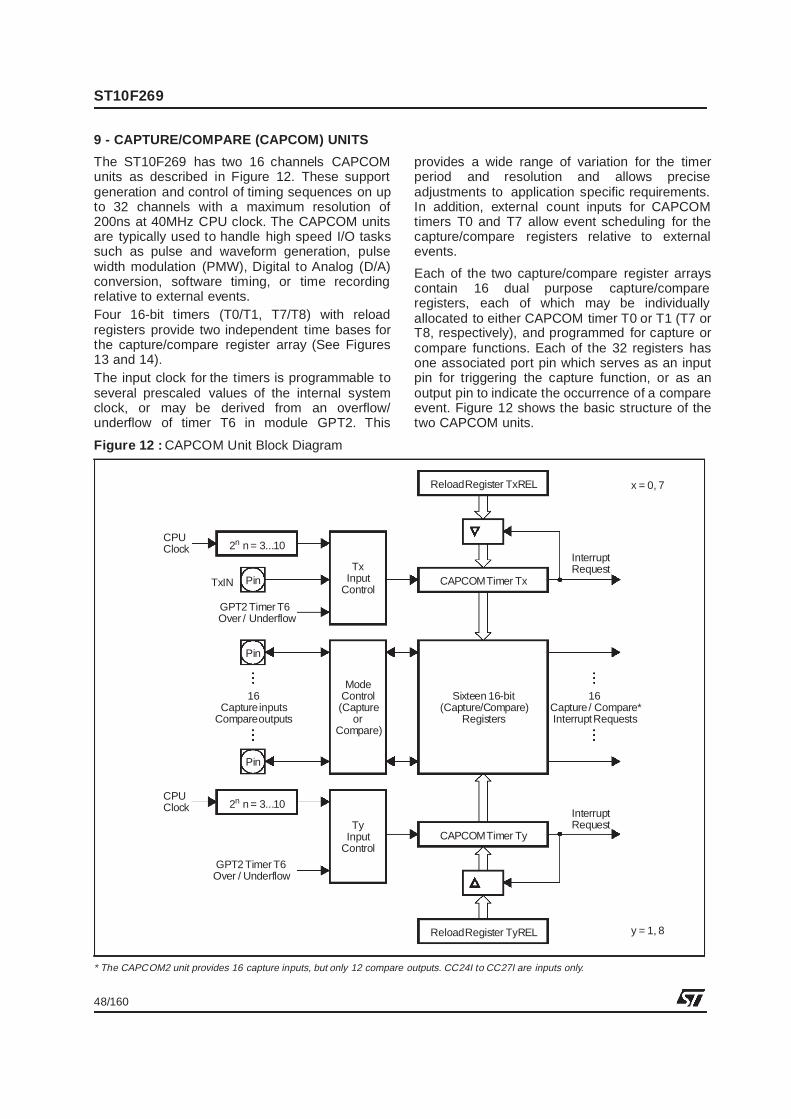
ST10F269
48/160
9 - CAPTURE/COMPARE (CAPCOM) UNITS
The ST10F269 has two 16 channels CAPCOMunits as described in Figure 12. These supportgeneration and control of timing sequences on upto 32 channels with a maximum resolution of200ns at 40MHz CPU clock. The CAPCOM unitsare typically used to handle high speed I/O taskssuch as pulse and waveform generation, pulsewidth modulation (PMW), Digital to Analog (D/A)conversion, software timing, or time recordingrelative to external events.Four 16-bit timers (T0/T1, T7/T8) with reloadregisters provide two independent time bases forthe capture/compare register array (See Figures13 and 14).The input clock for the timers is programmable toseveral prescaled values of the internal systemclock, or may be derived from an overflow/underflow of timer T6 in module GPT2. This
provides a wide range of variation for the timerperiod and resolution and allows preciseadjustments to application specific requirements.In addition, external count inputs for CAPCOMtimers T0 and T7 allow event scheduling for thecapture/compare registers relative to externalevents.
Each of the two capture/compare register arrayscontain 16 dual purpose capture/compareregisters, each of which may be individuallyallocated to either CAPCOM timer T0 or T1 (T7 orT8, respectively), and programmed for capture orcompare functions. Each of the 32 registers hasone associated port pin which serves as an inputpin for triggering the capture function, or as anoutput pin to indicate the occurrence of a compareevent. Figure 12 shows the basic structure of thetwo CAPCOM units.
* The CAPCOM2 unit provides 16 capture inputs, but only 12 compare outputs. CC24I to CC27I are inputs only.
Figure 12 : CAPCOM Unit Block Diagram
PinTx
InputControl
2n n = 3...10
GPT2 Timer T6
Pin
TxIN
CPUClock
ModeControl(Capture
orCompare)
16Captureinputs
Compareoutputs
Pin
TyInput
Control
2n n = 3...10
GPT2 Timer T6Over / Underflow
CPUClock
ReloadRegister TxREL
CAPCOMTimer Tx
InterruptRequest
Sixteen 16-bit(Capture/Compare)
Registers
Over / Underflow
CAPCOMTimer Ty
ReloadRegister TyREL
16Capture/ Compare*InterruptRequests
InterruptRequest
x = 0, 7
y = 1, 8

ST10F269
49/160
Figure 13 : Block Diagram of CAPCOM Timers T0 and T7
Figure 14 : Block Diagram of CAPCOM Timers T1 and T8
Note: When an external input signal isconnected to the input lines of both T0 andT7, these timers count the input signalsynchronously. Thus the two timers can beregarded as one timer whose contents canbe compared with 32 capture registers.
When a capture/compare register has beenselected for capture mode, the current contents ofthe allocated timer will be latched (captured) intothe capture/compare register in response to anexternal event at the port pin which is associatedwith this register. In addition, a specific interruptrequest for this capture/compare register isgenerated.
Either a positive, a negative, or both a positive anda negative external signal transition at the pin canbe selected as the triggering event. The contentsof all registers which have been selected for one
of the five compare modes are continuouslycompared with the contents of the allocatedtimers.
When a match occurs between the timer valueand the value in a capture /compare register,specific actions will be taken based on theselected compare mode (see Table 9).
The input frequencies fTx, for the timer inputselector Tx, are determined as a function of theCPU clocks. The timer input frequencies,resolution and periods which result from theselected pre-scaler option in TxI when using a40MHz CPU clock are listed in the Table 10.
The numbers for the timer periods are based on areload value of 0000h. Note that some numbersmay be rounded to 3 significant figures.
Pin
X
Txl
CPUClock
TxR
MUXGPT2 Timer T6Over / Underflow
Edge Select
TxIN
Txl
Txl TxM
InputControl
ReloadRegister TxREL
CAPCOMTimer Tx TxIRInterruptRequest
x = 0, 7
X
Txl
CPUClock
TxR
MUXGPT2 Timer T6Over / Underflow
TxM
Reload Register TxREL
CAPCOMTimer Tx TxIRInterruptRequest
x = 1, 8

ST10F269
50/160
Table 9 : Compare Modes
Compare Modes Function
Mode 0 Interrupt-only compare mode; several compare interrupts per timer period are possible
Mode 1 Pin toggles on each compare match; several compare events per timer period are possible
Mode 2 Interrupt-only compare mode; only one compare interrupt per timer period is generated
Mode 3 Pin set `1' on match; pin reset `0' on compare time overflow; only one compare event per timerperiod is generated
Double RegisterMode
Two registers operate on one pin; pin toggles on each compare match; several compare eventsper timer period are possible.
Table 10 : CAPCOM Timer Input Frequencies, Resolution and Periods
fCPU = 40MHzTimer Input Selection TxI
000b 001b 010b 011b 100b 101b 110b 111b
Pre-scaler for fCPU 8 16 32 64 128 256 512 1024
Input Frequency 5MHz 2.5MHz 1.25MHz 625kHz 312.5kHz 156.25kHz 78.125kHz 39.1kHz
Resolution 200ns 400ns 0.8 m s 1.6m s 3.2 m s 6.4m s 12.8m s 25.6 m s
Period 13.1ms 26.2ms 52.4ms 104.8ms 209.7ms 419.4ms 838.9ms 1.678s

ST10F269
51/160
10 - GENERAL PURPOSE TIMER UNIT
The GPT unit is a flexible multifunctional timer/counter structure which is used for time relatedtasks such as event timing and counting, pulsewidth and duty cycle measurements, pulsegeneration, or pulse multiplication. The GPT unitcontains five 16-bit timers organized into twoseparate modules GPT1 and GPT2. Each timer ineach module may operate independently inseveral different modes, or may be concatenatedwith another timer of the same module.
10.1 - GPT1
Each of the three timers T2, T3, T4 of the GPT1module can be configured individually for one offour basic modes of operation: timer , gatedtimer , counter mode and incremental interfacemode .
In timer mode, the input clock for a timer is derivedfrom the CPU clock, divided by a programmableprescaler.
In counter mode, the timer is clocked in referenceto external events.
Pulse width or duty cycle measurement issupported in gated timer mode where theoperation of a timer is controlled by the `gate' levelon an external input pin. For these purposes, eachtimer has one associated port pin (TxIN) whichserves as gate or clock input.
Table 11 lists the timer input frequencies,resolution and periods for each pre-scaler optionat 40MHz CPU clock. This also applies to theGated Timer Mode of T3 and to the auxiliarytimers T2 and T4 in Timer and Gated Timer Mode.The count direction (up/down) for each timer isprogrammable by software or may be altered
dynamically by an external signal on a port pin(TxEUD).
In Incremental Interface Mode, the GPT1 timers(T2, T3, T4) can be directly connected to theincremental position sensor signals A and B bytheir respective inputs TxIN and TxEUD.
Direction and count signals are internally derivedfrom these two input signals so that the contentsof the respective timer Tx corresponds to thesensor position. The third position sensor signalTOP0 can be connected to an interrupt input.
Timer T3 has output toggle latches (TxOTL) whichchanges state on each timer over flow / underflow.The state of this latch may be output on port pins(TxOUT) for time out monitoring of externalhardware components, or may be used internallyto clock timers T2 and T4 for high resolution oflong duration measurements.
In addition to their basic operating modes, timersT2 and T4 may be configured as reload or captureregisters for timer T3. When used as capture orreload registers, timers T2 and T4 are stopped.The contents of timer T3 is captured into T2 or T4in response to a signal at their associated inputpins (TxIN).
Timer T3 is reloaded with the contents of T2 or T4triggered either by an external signal or by aselectable state transition of its toggle latchT3OTL. When both T2 and T4 are configured toalternately reload T3 on opposite state transitionsof T3OTL with the low and high times of a PWMsignal, this signal can be constantly generatedwithout software intervention.
Table 11 : GPT1 Timer Input Frequencies, Resolution and Periods
fCPU = 40MHzTimer Input Selection T2I / T3I / T4I
000b 001b 010b 011b 100b 101b 110b 111b
Pre-scaler factor 8 16 32 64 128 256 512 1024
Input Freq 5MHz 2.5MHz 1.25MHz 625kHz 312.5kHz 156.25kHz 78.125kHz 39.1kHz
Resolution 200ns 400ns 0.8m s 1.6m s 3.2 m s 6.4m s 12.8m s 25.6m s
Period maximum 13.1ms 26.2ms 52.4ms 104.8ms 209.7ms 419.4ms 838.9ms 1.678s

ST10F269
52/160
Figure 15 : Block Diagram of GPT1
10.2 - GPT2The GPT2 module provides precise event controland time measurement. It includes two timers (T5,T6) and a capture/reload register (CAPREL). Bothtimers can be clocked with an input clock which isderived from the CPU clock via a programmableprescaler or with external signals. The countdirection (up/down) for each timer isprogrammable by software or may additionally bealtered dynamically by an external signal on a portpin (TxEUD). Concatenation of the timers issupported via the output toggle latch (T6OTL) oftimer T6 which changes its state on each timeroverflow/underflow.The state of this latch may be used to clock timerT5, or it may be output on a port pin (T6OUT). Theoverflow / underflow of timer T6 can additionallybe used to clock the CAPCOM timers T0 or T1,
and to cause a reload from the CAPREL register.The CAPREL register may capture the contents oftimer T5 based on an external signal transition onthe corresponding port pin (CAPIN), and timer T5may optionally be cleared after the captureprocedure. This allows absolute time differencesto be measured or pulse multiplication to beperformed without software overhead.The capture trigger (timer T5 to CAPREL) mayalso be generated upon transitions of GPT1 timerT3 inputs T3IN and/or T3EUD. This isadvantageous when T3 operates in IncrementalInterface Mode.Table 12 lists the timer input frequencies,resolution and periods for each pre-scaler optionat 40MHz CPU clock. This also applies to theGated Timer Mode of T6 and to the auxiliary timerT5 in Timer and Gated Timer Mode.
2n n=3...10
2n n=3...10
2n n=3...10
T2EUD
T2IN
CPUClock
CPUClock
CPU Clock
T3IN
T4IN
T3EUD
T4EUD
T2ModeControl
T3ModeControl
T4ModeControl
GPT1 Timer T2
GPT1 Timer T3
GPT1 Timer T4
T3OTL
ReloadCapture
U/D
U/D
ReloadCapture
InterruptRequest
InterruptRequest
InterruptRequest
T3OUT
U/D
Table 12 : GPT2 Timer Input Frequencies, Resolution and Period
fCPU = 40MHzTimer Input Selection T5I / T6I
000b 001b 010b 011b 100b 101b 110b 111b
Pre-scaler factor 4 8 16 32 64 128 256 512
Input Freq 10MHz 5MHz 2.5MHz 1.25MHz 625kHz 312.5kHz 156.25kHz 78.125kHz
Resolution 100ns 200ns 400ns 0.8m s 1.6m s 3.2m s 6.4 m s 12.8m s
Period maximum 6.55ms 13.1ms 26.2ms 52.4ms 104.8ms 209.7ms 419.4ms 838.9ms

ST10F269
53/160
Figure 16 : Block Diagram of GPT2
2n n=2...9
2n n=2...9
T5EUD
T5IN
CPUClock
CPUClock
T6IN
T6EUD
T5ModeControl
T6ModeControl
GPT2 Timer T5
GPT2 Timer T6
U/D
InterruptRequest
U/D
GPT2 CAPREL
T60TL
Toggle FF
T6OUT
CAPIN
Reload InterruptRequest
to CAPCOMTimers
Capture
Clear
InterruptRequest

ST10F269
54/160
11 - PWM MODULE
The pulse width modulation module can generateup to four PWM output signals using edge-alignedor centre-aligned PWM. In addition, the PWMmodule can generate PWM burst signals and
single shot outputs. TheTable 13 shows the PWMfrequencies for different resolutions. The level ofthe output signals is selectable and the PWMmodule can generate interrupt requests.
Figure 17 : Block Diagram of PWM Module
Table 13 : PWM Unit Frequencies and Resolution at 40MHz CPU Clock
Mode 0 Resolution 8-bit 10-bit 12-bit 14-bit 16-bit
CPU Clock/1 25ns 156.25kHz 39.1kHz 9.77kHz 2.44Hz 610Hz
CPU Clock/64 1.6 m s 2.44Hz 610Hz 152.6Hz 38.15Hz 9.54Hz
Mode 1 Resolution 8-bit 10-bit 12-bit 14-bit 16-bit
CPU Clock/1 25ns 78.12kHz 19.53kHz 4.88kHz 1.22kHz 305.17Hz
CPU Clock/64 1.6 m s 1.22kHz 305.17Hz 76.29Hz 19.07Hz 4.77Hz
PPx Period Register
Comparator
PTx16-bit Up/DownCounter
ShadowRegister
PWx Pulse Width Register
Input
RunControl
Clock 1
Clock 2
Comparator
*
*
*
Up/Down/Clear Control
Match
Output ControlMatch
WriteControl
* User readable/ writeableregister
EnablePOUTx

ST10F269
55/160
12 - PARALLEL PORTS
12.1 - IntroductionThe ST10F269 MCU provides up to 111 I/O lineswith programmable features. These capabilitiesbring very flexible adaptation of this MCU to widerange of applications.
ST10F269 has 9 groups of I/O lines gathered asfollowing:± Port 0 is a 2 time 8-bit port named P0L (Low as
less significant Byte) and P0H (high as most sig-nificant Byte)
± Port 1 is a 2 time 8-bit port named P1L and P1H± Port 2 is a 16-bit port
± Port 3 is a 15-bit port (P3.14 line is not imple-mented)
± Port 4 is a 8-bit port
± Port 5 is a 16-bit port input only
± Port 6, Port 7 and Port 8 are 8-bit portThese ports may be used as general purposebidirectionnal input or output, software controlledwith dedicated registers.
For example the output drivers of six of the ports(2, 3, 4, 6, 7, 8) can be configured (bit-wise) forpush-pull or open drain operation using ODPxregisters.
In addition, the sink and the source capability andthe rise / fall time of the transition of the signal ofsome of the push-pull buffers can be programmed
to fit the driving requirements of the applicationand to minimize EMI. This feature is implementedon Port 0, 1, 2, 3, 4, 6, 7 and 8 with the controlregisters POCONx. The output drivers capabilitiesof ALE, RD, WR control lines are programmablewith the dedicated bits of POCON20 controlregister.
The input threshold levels are programmable(TTL/CMOS) for 5 ports (2, 3, 4, 7, 8). The logiclevel of a pin is clocked into the input latch onceper state time, regardless whether the port isconfigured for input or output. The threshold isselected with the PICON register control bits.
A write operation to a port pin configured as aninput causes the value to be written into the portoutput latch, while a read operation returns thelatched state of the pin itself. A read-modify-writeoperation reads the value of the pin, modifies it,and writes it back to the output latch.
Writing to a pin configured as an output(DPx.y=`1') causes the output latch and the pin tohave the written value, since the output buffer isenabled. Reading this pin returns the value of theoutput latch. A read-modify-write operation readsthe value of the output latch, modifies it, andwrites it back to the output latch, thus alsomodifying the level at the pin.
I/O lines support an alternate function which isdetailed in the following description of each port.

ST10F269
56/160
Figure 18 : SFRs and Pins Associated with the Parallel Ports
Dat
aIn
put/
Out
putR
egis
ter
15 -
14 -
13 -
12 -
11 -
10 -
9 -
8 -
7 Y
6 Y
5 Y
4 Y
3 Y
2 Y
1 Y
0 YP
0L
--
--
--
--
YY
YY
YY
YY
P0H
--
--
--
--
YY
YY
YY
YY
P1L
--
--
--
--
YY
YY
YY
YY
P1H
YY
YY
YY
YY
YY
YY
YY
YY
P2
Y-
YY
YY
YY
YY
YY
YY
YY
P3
--
--
--
--
YY
YY
YY
YY
P4
YY
YY
YY
YY
YY
YY
YY
YY
P5
--
--
--
--
YY
YY
YY
YY
P6
--
--
--
--
YY
YY
YY
YY
P7
--
--
--
--
YY
YY
YY
YY
P8
Dire
ctio
nC
ontr
olR
egis
ters
15 -
14 -
13 -
12 -
11 -
10 -
9 -
8 -
7 Y
6 Y
5 Y
4 Y
3 Y
2 Y
1 Y
0 YD
P0L
--
--
--
--
YY
YY
YY
YY
DP
0H
--
--
--
--
YY
YY
YY
YY
DP
1L
--
--
--
--
YY
YY
YY
YY
DP
1H
YY
YY
YY
YY
YY
YY
YY
YY
DP
2
Y-
YY
YY
YY
YY
YY
YY
YY
DP
3
--
--
--
--
YY
YY
YY
YY
DP
4
--
--
--
--
YY
YY
YY
YY
DP
6
--
--
--
--
YY
YY
YY
YY
DP
7
--
--
--
--
YY
YY
YY
YY
DP
8
Thr
esho
ld/O
pen
Dra
inC
ontr
ol
15 -
14 -
13 -
12 -
11 -
10 -
9 -
8 -
7 Y
6 Y
5 -
4 Y
3 Y
2 Y
1 Y
0 YP
ICO
N
YY
YY
YY
YY
YY
YY
YY
YY
OD
P2
--
Y-
YY
YY
YY
YY
YY
YY
OD
P3
--
--
--
--
YY
--
--
--
OD
P4
--
--
--
--
YY
YY
YY
YY
OD
P6
--
--
--
--
YY
YY
YY
YY
OD
P7
--
--
--
--
YY
YY
YY
YY
OD
P8
Out
putD
river
Con
trol
Reg
iste
r
15 -
14 -
13 -
12 -
11 -
10 -
9 -
8 -
7 Y
6 Y
5 Y
4 Y
3 Y
2 Y
1 Y
0 YP
OC
ON
0L
--
--
--
--
YY
YY
YY
YY
PO
CO
N0H
--
--
--
--
YY
YY
YY
YY
PO
CO
N1L
--
--
--
--
YY
YY
YY
YY
PO
CO
N1H
YY
YY
YY
YY
YY
YY
YY
YY
PO
CO
N2
Y-
YY
YY
YY
YY
YY
YY
YY
PO
CO
N3
--
--
--
--
YY
YY
YY
YY
PO
CO
N4
--
--
--
--
YY
YY
YY
YY
PO
CO
N6
--
--
--
--
YY
YY
YY
YY
PO
CO
N7
--
--
--
--
YY
YY
YY
YY
PO
CO
N8
--
--
--
--
YY
YY
YY
YY
PO
CO
N20
*
*R
D,W
R,A
LElin
eson
ly
Y:
Bit
has
anI/O
func
tion
-:
Bit
has
noI/O
dedi
cate
dfu
nctio
nor
isno
tim
plem
ente
dR
egis
terb
elon
gsto
ES
FR
area
E:
YY
YY
YY
YY
YY
YY
YY
YY
P5D
IDIS
PIC
ON
:P
2LIN
P2H
INP
3LIN
P3H
INP
4LIN
P6L
IN(to
beim
plem
ente
d)P
7LIN
P8L
IN
E E E E
E E E E E E E
E E E E E E E E E E E

ST10F269
57/160
12.2 - I/O's Special Features
12.2.1 - Open Drain Mode
Some of the I/O ports of ST10F269 support theopen drain capability. This programmable featuremay be used with an external pull-up resistor, inorder to get an AND wired logical function.
This feature is implemented for ports P2, P3, P4,P6, P7 and P8 (see respective sections), and iscontrolled through the respective Open DrainControl Registers ODPx. These registers allowthe individual bit-wise selection of the open drainmode for each port line. If the respective controlbit ODPx.y is `0' (default after reset), the outputdriver is in the push-pull mode. If ODPx.y is `1', theopen drain configuration is selected. Note that allODPx registers are located in the ESFR space(See Figure 19).
12.2.2 - Input Threshold Control
The standard inputs of the ST10F269 determinethe status of input signals according to TTL levels.In order to accept and recognize noisy signals,CMOS-like input thresholds can be selectedinstead of the standard TTL thresholds for all pinsof Port 2, Port 3, Port 4, Port 7 and Port 8. Thesespecial thresholds are defined above the TTLthresholds and feature a defined hysteresis toprevent the inputs from toggling while therespective input signal level is near the thresholds.
The Port Input Control register PICON is used toselect these thresholds for each Byte of theindicated ports, this means the 8-bit ports P4, P7and P8 are controlled by one bit each while portsP2 and P3 are controlled by two bits each.
All options for individual direction and output modecontrol are available for each pin, independent ofthe selected input threshold. The input hysteresisprovides stable inputs from noisy or slowlychanging external signals (See Figure 20).
PICON (F1C4h / E2h) ESFR ResetValue:--00h
15 14 13 12 11 10 9 8 7 6 5 4 3 2 1 0
- - - - - - - - P8LIN P7LIN - P4LIN P3HIN P3LIN P2HIN P2LIN
RW RW RW RW RW RW RW
Bit Function
PxLIN Port x Low Byte Input Level Selection
0: Pins Px.7...Px.0 switch on standard TTL input levels1: Pins Px.7...Px.0 switch on special threshold input levels
PxHIN Port x High Byte Input Level Selection
0: Pins Px.15...Px.8 switch on standard TTL input levels1: Pins Px.15...Px.8 switch on special threshold input levels
Figure 19 : Output Drivers in Push-pull Mode and in Open Drain Mode
Pin
Q
Push-Pull Output Driver
Q
Open Drain Output Driver
ExternalPullup
Pin

ST10F269
58/160
12.2.3 - Output Driver ControlThe port output control registers POCONx allowto select the port output driver characteristics of aport. The aim of these selections is to adapt theoutput drivers to the application's requirements,and to improve the EMI behaviour of the device.Two characteristics may be selected:Edge characteristic defines the rise/fall time forthe respective output. Slow edges reduce thepeak currents that are sinked/sourced whenchanging the voltage level of an externalcapacitive load. For a bus interface or pins thatare changing at frequency higher than 1MHz,however, fast edges may still be required.Driver characteristic defines either the generaldriving capability of the respective driver, or if the
driver strength is reduced after the target outputlevel has been reached or not. Reducing thedriver strength increases the output's internalresistance, which attenuates noise that isimported via the output line. For driving LEDs orpower transistors, however, a stable high outputcurrent may still be required as described below.
This rise / fall time of 4 I/O pads (a nibble) isselected using 2-bit named PNxEC. That meansPort Nibble (x = nibble number, it could be 3 as forPort 2.15 to 2.12)Edge Characteristic.
The sink / source capability of the same 4 I/Opads is selected using 2-bit namedPNxDC. Thatmeans Port Nibble (x = nibble number) DriveCharacteristic (See Table 14).
POCONx (F0yyh / zzh) for 8-bit Ports ESFR Reset Value: --00h
POCONx (F0yyh / zzh) for 16-bit Ports ESFR ResetValue: 0000h
Note: In case of reading an 8 bit P0CONX register, high Byte ( bit 15..8) is read as 00h
Figure 20 : Hysteresis for Special Input Thresholds
Input level
Bit state
Hysteresis
15 14 13 12 11 10 9 8 7 6 5 4 3 2 1 0
- - - - - - - - PN1DC PN1EC PN0DC PN0EC
RW RW RW RW
15 14 13 12 11 10 9 8 7 6 5 4 3 2 1 0
PN3DC PN3EC PN2DC PN2EC PN1DC PN1EC PN0DC PN0EC
RW RW RW RW RW RW RW RW
Bit Function
PNxEC Port Nibble x Edge Characteristic (rise/fall time)00: Fast edge mode, rise/fall times depend on the size of the driver.01: Slow edge mode, rise/fall times ~60 ns10: Reserved11: Reserved
PNxDC Port Nibble x Driver Characteristic (output current)00: High Current mode:
Driver always operates with maximum strength.01: Dynamic Current mode:
Driver strength is reduced after the target level has been reached.10: Low Current mode:
Driver always operates with reduced strength.11: Reserved

ST10F269
59/160
The table lists the defined POCON registers and the allocation of control bit-fields and port pins.
Dedicated Pins Output Control
Programmable pad drivers also are supported for the dedicated pins ALE,RD and WR. For these pads,a special POCON20 register is provided.
POCON20 (F0AAh / 55h) ESFR Reset Value: --00h
Table 14 : Port Control Register Allocation
ControlRegister
PhysicalAddress
8-bitAddress
Controlled Port Nibble
3 2 1 0
POCON0L F080h 40h P0L.7...4 P0L.3...0
POCON0H F082h 41h P0H.7...4 P0H.3...0
POCON1L F084h 42h P1L.7...4 P1L.3...0
POCON1H F086h 43h P1H.7...4 P1H.3...0
POCON2 F088h 44h P2.15...12 P2.11...8 P2.7...4 P2.3...0
POCON3 F08Ah 45h P3.15, 3.13, 3.12 P3.11...8 P3.7...4 P3.3...0
POCON4 F08Ch 46h P4.7...4 P4.3...0
POCON6 F08Eh 47h P6.7...4 P6.3...0
POCON7 F090h 48h P7.7...4 P7.3...0
POCON8 F092h 49h P8.7...4 P8.3...0
15 14 13 12 11 10 9 8 7 6 5 4 3 2 1 0
- - - - - - - - PN1DC PN1EC PN0DC PN0EC
RW RW RW RW
PN0EC RD, WR Edge Characteristic (rise/fall time)00: Fast edge mode, rise/fall times depend on the size of the driver.01: Slow edge mode, rise/fall times ~60 ns10: Reserved11: Reserved
PN0DC RD, WR Driver Characteristic (output current)00: High Current mode:
Driver always operates with maximum strength.01: Dynamic Current mode:
Driver strength is reduced after the target level has been reached.10: Low Current mode:
Driver always operates with reduced strength.11: Reserved
PN1EC ALE Edge Characteristic (rise/fall time)00: Fast edge mode, rise/fall times depend on the size of the driver.01: Slow edge mode, rise/fall times ~60 ns10: Reserved11: Reserved
PN1DC ALE Driver Characteristic (output current)00: High Current mode:
Driver always operates with maximum strength.01: Dynamic Current mode:
Driver strength is reduced after the target level has been reached.10: Low Current mode:
Driver always operates with reduced strength.11: Reserved

ST10F269
60/160
12.2.4 - Alternate Port Functions
Each port line has one associated programmablealternate input or output function.
± PORT0 and PORT1 may be used as addressand data lines when accessing external memory.
± Port 2, Port 7 and Port 8 are associated with thecapture inputs or compare outputs of the CAP-COM units and/or with the outputs of the PWMmodule.Port 2 is also used for fast external interrupt in-puts and for timer 7 input.
± Port 3 includes the alternate functions of timers,serial interfaces, the optional bus control signalBHE and the system clock output (CLKOUT).
± Port 4 outputs the additional segment addressbit A16 to A23 in systems where segmentationis enabled to access more than 64K Bytes ofmemory.
± Port 5 is used as analog input channels of theA/D converter or as timer control signals.
± Port 6 provides optional bus arbitration signals(BREQ, HLDA, HOLD) and chip select signals.
If an alternate output function of a pin is to beused, the direction of this pin must beprogrammed for output (DPx.y=`1'), except forsome signals that are used directly after reset andare configured automatically. Otherwise the pinremains in the high-impedance state and is noteffected by the alternate output function. Therespective port latch should hold a `1', because itsoutput is ANDed with the alternate output data(except for PWM output signals).
If an alternate input function of a pin is used, thedirection of the pin must be programmed for input(DPx.y=`0') if an external device is driving the pin.The input direction is the default after reset. If noexternal device is connected to the pin, however,one can also set the direction for this pin to output.
In this case, the pin reflects the state of the portoutput latch. Thus, the alternate input functionreads the value stored in the port output latch.This can be used for testing purposes to allow asoftware trigger of an alternate input function bywriting to the port output latch.
On most of the port lines, the application softwaremust set the proper direction when using analternate input or output function of a pin. This isdone by setting or clearing the direction control bitDPx.y of the pin before enabling the alternatefunction. There are port lines, however, where thedirection of the port line is switched automatically.
For instance, in the multiplexed external busmodes of PORT0, the direction must be switchedseveral times for an instruction fetch in order tooutput the addresses and to input the data.Obviously, this cannot be done throughinstructions. In these cases, the direction of theport line is switched automatically by hardware ifthe alternate function of such a pin is enabled.To determine the appropriate level of the portoutput latches check how the alternate dataoutput is combined with the respective port latchoutput.
There is one basic structure for all port linessupporting only one alternate input function. Portlines with only one alternate output function,however, have different structures. It has to beadapted to support the normal and the alternatefunction features.
All port lines that are not used for these alternatefunctions may be used as general purpose I/Olines. When using port pins for general purposeoutput, the initial output value should be written tothe port latch prior to enabling the output drivers,in order to avoid undesired transitions on theoutput pins. This applies to single pins as well asto pin groups (see examples below).
SINGLE_BIT: BSET P4.7 ; Init ial output level is ”high”
BSET DP4.7 ; Switch on the output driver
BIT_GROUP: BFLDH P4, #24H, #24H ; Init ial output level is ”high”
BFLDH DP4, #24H, #24H ; Switch on the output drivers
Note: When using several BSET pairs to control more pins of one port, these pairs must be separated byinstructions, which do not apply to the respective port (SeeChapter 6 - Central Processing Unit(CPU)).

ST10F269
61/160
12.3 - PORT0The two 8-bit ports P0H and P0L represent thehigher and lower part of PORT0, respectively.Both halves of PORT0 can be written (via a PECtransfer) without effecting the other half.
If this port is used for general purpose I/O, thedirection of each line can be configured via thecorresponding direction registers DP0H andDP0L.
P0L (FF00h / 80h) SFR Reset Value: --00h
P0H (FF02h / 81h) SFR Reset Value: --00h
DP0L (F100h / 80h) ESFR Reset Value: --00h
DP0H (F102h / 81h) ESFR Reset Value: --00h
15 14 13 12 11 10 9 8 7 6 5 4 3 2 1 0
- - - - - - - - P0L.7 P0L.6 P0L.5 P0L.4 P0L.3 P0L.2 P0L.1 P0L.0
RW RW RW RW RW RW RW RW
15 14 13 12 11 10 9 8 7 6 5 4 3 2 1 0
- - - - - - - - P0H.7 P0H.6 P0H.5 P0H.4 P0H.3 P0H.2 P0H.1 P0H.0
RW RW RW RW RW RW RW RW
P0X.y Port Data Register P0H or P0L Bit y
15 14 13 12 11 10 9 8 7 6 5 4 3 2 1 0
- - - - - - - - DP0L.7 DP0L.6 DP0L.5 DP0L.4 DP0L.3 DP0L.2 DP0L.1 DP0L.0
RW RW RW RW RW RW RW RW
15 14 13 12 11 10 9 8 7 6 5 4 3 2 1 0
- - - - - - - - DP0H.7 DP0H.6 DP0H.5 DP0H.4 DP0H.3 DP0H.2 DP0H.1 DP0H.0
RW RW RW RW RW RW RW RW
DP0X.y Port Direction Register DP0H or DP0L Bit yDP0X.y = 0: Port line P0X.y is an input (high-impedance)DP0X.y = 1: Port line P0X.y is an output
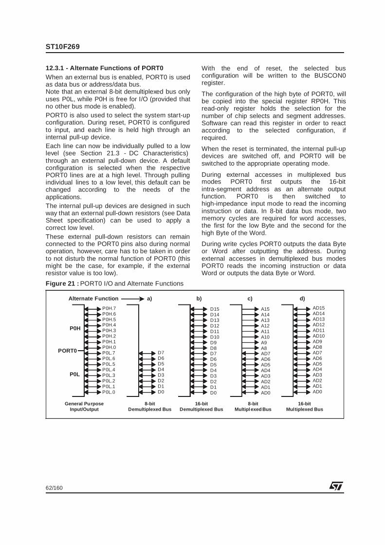
ST10F269
62/160
12.3.1 - Alternate Functions of PORT0When an external bus is enabled, PORT0 is usedas data bus or address/data bus.Note that an external 8-bit demultiplexed bus onlyuses P0L, while P0H is free for I/O (provided thatno other bus mode is enabled).PORT0 is also used to select the system start-upconfiguration. During reset, PORT0 is configuredto input, and each line is held high through aninternal pull-up device.Each line can now be individually pulled to a lowlevel (see Section 21.3 - DC Characteristics)through an external pull-down device. A defaultconfiguration is selected when the respectivePORT0 lines are at a high level. Through pullingindividual lines to a low level, this default can bechanged according to the needs of theapplications.The internal pull-up devices are designed in suchway that an external pull-down resistors (see DataSheet specification) can be used to apply acorrect low level.These external pull-down resistors can remainconnected to the PORT0 pins also during normaloperation, however, care has to be taken in orderto not disturb the normal function of PORT0 (thismight be the case, for example, if the externalresistor value is too low).
With the end of reset, the selected busconfiguration will be written to the BUSCON0register.
The configuration of the high byte of PORT0, willbe copied into the special register RP0H. Thisread-only register holds the selection for thenumber of chip selects and segment addresses.Software can read this register in order to reactaccording to the selected configuration, ifrequired.
When the reset is terminated, the internal pull-updevices are switched off, and PORT0 will beswitched to the appropriate operating mode.
During external accesses in multiplexed busmodes PORT0 first outputs the 16-bitintra-segment address as an alternate outputfunction. PORT0 is then switched tohigh-impedance input mode to read the incominginstruction or data. In 8-bit data bus mode, twomemory cycles are required for word accesses,the first for the low Byte and the second for thehigh Byte of the Word.
During write cycles PORT0 outputs the data Byteor Word after outputting the address. Duringexternal accesses in demultiplexed bus modesPORT0 reads the incoming instruction or dataWord or outputs the data Byte or Word.
Figure 21 : PORT0 I/O and Alternate Functions
P0H.7P0H.6P0H.5P0H.4P0H.3P0H.2P0H.1P0H.0P0L.7P0L.6P0L.5P0L.4P0L.3P0L.2P0L.1P0L.0
PORT0
P0H
P0L
Alternate Function a) b) c) d)
General PurposeInput/Output
8-bitDemultiplexed Bus
16-bitDemultiplexed Bus
8-bitMultipl exed Bus
16-bitMultiplexed Bus
D7D6D5D4D3D2D1D0
D15D14D13D12D11D10D9D8D7D6D5D4D3D2D1D0
A15A14A13A12A11A10A9A8AD7AD6AD5AD4AD3AD2AD1AD0
AD15AD14AD13AD12AD11AD10AD9AD8AD7AD6AD5AD4AD3AD2AD1AD0

ST10F269
63/160
When an external bus mode is enabled, thedirection of the port pin and the loading of datainto the port output latch are controlled by the buscontroller hardware.The input of the port output Buffer is disconnectedfrom the internal bus and is switched to the linelabeled ªAlternate Data Outputº via a multiplexer.The alternate data can be the 16-bit intra-segmentaddress or the 8/16-bit data information. Theincoming data on PORT0 is read on the line
ªAlternate Data Inputº. While an external busmode is enabled, the user software should notwrite to the port output latch, otherwiseunpredictable results may occur.
When the external bus modes are disabled, thecontents of the direction register last written by theuser becomes active.
The Figure 22 shows the structure of a PORT0pin.
Figure 22 : Block Diagram of a PORT0 Pin
DirectionLatch
Write DP0H.y / DP0L.y
Read DP0H.y / DP0L.y
Port OutputLatch
Write P0H.y / P0L.y
Read P0H.y / P0L.y
Inte
rnal
Bus
MUX
0
1
MUX
0
1
AlternateDataOutput
MUX
0
1AlternateDirection
InputLatch
Clock
P0H.yP0L.yOutput
Buffer
y = 7...0
AlternateFunctionEnable
Port DataOutput

ST10F269
64/160
12.4 - PORT1
The two 8-bit ports P1H and P1L represent the higher and lower part of PORT1, respectively. Both halvesof PORT1 can be written (via a PEC transfer) without effecting the other half.
If this port is used for general purpose I/O, the direction of each line can be configured via thecorresponding direction registers DP1H and DP1L.
P1L (FF04h / 82h) SFR Reset Value: --00h
P1H (FF06h / 83h) SFR Reset Value: --00h
DP1L (F104h / 82h) ESFR Reset Value: --00h
DP1H (F106h / 83h) ESFR Reset Value: --00h
12.4.1 - Alternate Functions of PORT1
When a demultiplexed external bus is enabled, PORT1 is used as address bus.Note: Demultiplexed bus modes use PORT1 as a 16-bit port. Otherwise all 16 port lines can be used forgeneral purpose I/O.
The upper 4 pins of PORT1 (P1H.7...P1H.4) are used as capture input lines (CC27IO...CC24IO).
During external accesses in demultiplexed bus modes PORT1 outputs the 16-bit intra-segment addressas an alternate output function.
During external accesses in multiplexed bus modes, whenno BUSCON register selects a demultiplexedbus mode, PORT1 is not used and is available for general purpose I/O.
15 14 13 12 11 10 9 8 7 6 5 4 3 2 1 0
- - - - - - - - P1L.7 P1L.6 P1L.5 P1L4 P1L.3 P1L.2 P1L.1 P1L.0
RW RW RW RW RW RW RW RW
15 14 13 12 11 10 9 8 7 6 5 4 3 2 1 0
- - - - - - - - P1H.7 P1H.6 P1H.5 P1H.4 P1H.3 P1H.2 P1H.1 P1H.0
RW RW RW RW RW RW RW RW
P1X.y Port Data Register P1H or P1L Bit y
15 14 13 12 11 10 9 8 7 6 5 4 3 2 1 0
- - - - - - - - DP1L.7 DP1L.6 DP1L.5 DP1L.4 DP1L.3 DP1L.2 DP1L.1 DP1L.0
RW RW RW RW RW RW RW RW
15 14 13 12 11 10 9 8 7 6 5 4 3 2 1 0
- - - - - - - - DP1H.7 DP1H.6 DP1H.5 DP1H.4 DP1H.3 DP1H.2 DP1H.1 DP1H.0
RW RW RW RW RW RW RW RW
DP1X.y Port Direction Register DP1H or DP1L Bit yDP1X.y = 0: Port line P1X.y is an input (high-impedance)DP1X.y = 1: Port line P1X.y is an output

ST10F269
65/160
Figure 23 : PORT1 I/O and Alternate Functions
When an external bus mode is enabled, thedirection of the port pin and the loading of datainto the port output latch are controlled by the buscontroller hardware.The input of the port Buffer latch is disconnectedfrom the internal bus and is switched to the linelabeled ªAlternate Data Outputº via a multiplexer.The alternate data is the 16-bit intra-segment
address. While an external bus mode is enabled,the user software should not write to the portoutput latch, otherwise unpredictable results mayoccur. When the external bus modes are disabled,the contents of the direction register last written bythe user becomes active.The Figure 24 shows the structure of a PORT1pin.
PORT1
P1H
P1L
Alternate Function a)
General Purpose Input/Out put 8/16-bit Demultiplexed Bus
b)
CAPCOM2 Capture Inputs only
P1H.7P1H.6P1H.5P1H.4P1H.3P1H.2P1H.1P1H.0P1L.7P1L.6P1L.5P1L.4P1L.3P1L.2P1L.1P1L.0
A15A14A13A12A11A10A9A8A7A6A5A4A3A2A1A0
CC27IOCC26IOCC25IOCC24IO
Figure 24 : Block Diagram of a PORT1 Pin
DirectionLatch
Write DP1H.y / DP1L.y
Read DP1H.y / DP1L.y
Port OutputLatch
Write P1H.y / P1L.y
Read P1H.y / P1L.y
Inte
rnal
Bus
MUX
0
1
MUX
0
1
MUX
0
1ª1º
InputLatch
Clock
P1H.yP1L.yOutput
Buffer
y = 7...0
AlternateFunctionEnable
Port DataOutput
AlternateDataOutput

ST10F269
66/160
12.5 - Port 2If this 16-bit port is used for general purpose I/O, the direction of each line can be configured via thecorresponding direction register DP2. Each port line can be switched into push/pull or open drain modevia the open drain control register ODP2.
P2 (FFC0h / E0h) SFR Reset Value: 0000h
DP2 (FFC2h / E1h) SFR Reset Value: 0000h
ODP2 (F1C2h / E1h) ESFR Reset Value: 0000h
12.5.1 - Alternate Functions of Port 2All Port 2 lines (P2.15...P2.0) serve as captureinputs or compare outputs (CC15IO...CC0IO) forthe CAPCOM1 unit.When a Port 2 line is used as a capture input, thestate of the input latch, which represents the stateof the port pin, is directed to the CAPCOM unit viathe line ªAlternate Pin Data Inputº. If an externalcapture trigger signal is used, the direction of therespective pin must be set to input.If the direction is set to output, the state of the portoutput latch will be read since the pin representsthe state of the output latch.This can be used to trigger a capture eventthrough software by setting or clearing the portlatch. Note that in the output configuration, noexternal device may drive the pin, otherwiseconflicts would occur.
When a Port 2 line is used as a compare output(compare modes 1 and 3), the compare event (orthe timer overflow in compare mode 3) directlyeffects the port output latch. In compare mode 1,when a valid compare match occurs, the state ofthe port output latch is read by the CAPCOMcontrol hardware via the line ªAlternate Latch DataInputº, inverted, and written back to the latch viathe line ªAlternate Data Outputº.
The port output latch is clocked by the signalªCompare Triggerº which is generated by theCAPCOM unit. In compare mode 3, when a matchoccurs, the value '1' is written to the port outputlatch via the line ªAlternate Data Outputº. Whenan overflow of the corresponding timer occurs, a'0' is written to the port output latch. In both cases,the output latch is clocked by the signal ªCompareTriggerº.
15 14 13 12 11 10 9 8 7 6 5 4 3 2 1 0
P2.15 P2.14 P2.13 P2.12 P2.11 P2.10 P2.9 P2.8 P2.7 P2.6 P2.5 P2.4 P2.3 P2.2 P2.1 P2.0
RW RW RW RW RW RW RW RW RW RW RW RW RW RW RW RW
P2.y Port Data Register P2 Bit y
15 14 13 12 11 10 9 8 7 6 5 4 3 2 1 0
DP2
.15
DP2
.14
DP2
.13
DP2
.12
DP2
.11
DP2
.10
DP2
.9
DP2
.8
DP2
.7
DP2
.6
DP2
.5
DP2
.4
DP2
.3
DP2
.2
DP2
.1
DP2
.0
RW RW RW RW RW RW RW RW RW RW RW RW RW RW RW RW
DP2.y Port Direction Register DP2 Bit yDP2.y = 0: Port line P2.y is an input (high-impedance)DP2.y = 1: Port line P2.y is an output
15 14 13 12 11 10 9 8 7 6 5 4 3 2 1 0
ODP2
.15
ODP2
.14
ODP2
.13
ODP2
.12
ODP2
.11
ODP2
.10
ODP2
.9
ODP2
.8
ODP2
.7
ODP2
.6
ODP2
.5
ODP2
.4
ODP2
.3
ODP2
.2
ODP2
.1
ODP2
.0
RW RW RW RW RW RW RW RW RW RW RW RW RW RW RW RW
ODP2.y Port 2 Open Drain Control Register Bit yODP2.y = 0: Port line P2.y output driver in push/pull modeODP2.y = 1: Port line P2.y output driver in open drain mode

ST10F269
67/160
The direction of the pin should be set to output bythe user, otherwise the pin will be in thehigh-impedance state and will not reflect the stateof the output latch.
As can be seen from the port structure in Figure26, the user software always has free access tothe port pin even when it is used as a compareoutput. This is useful for setting up the initial levelof the pin when using compare mode 1 or thedouble-register mode. In these modes, unlike incompare mode 3, the pin is not set to a specificvalue when a compare match occurs, but istoggled instead.
When the user wants to write to the port pin at thesame time a compare trigger tries to clock theoutput latch, the write operation of the usersoftware has priority. Each time a CPU writeaccess to the port output latch occurs, the input
multiplexer of the port output latch is switched tothe line connected to the internal bus. The portoutput latch will receive the value from the internalbus and the hardware triggered change will belost.
As all other capture inputs, the capture inputfunction of pins P2.15...P2.0 can also be used asexternal interrupt inputs (200ns sample rate at40MHz CPU clock).
The upper eight Port 2 lines (P2.15...P2.8) alsocan serve as Fast External Interrupt inputs fromEX0IN to EX7IN (Fast external interrupt samplingrate is 25ns at 40MHz CPU clock).
P2.15 in addition serves as input for CAPCOM2timer T7 (T7IN). The Table 15 summarizes thealternate functions of Port 2.
Table 15 : Alternate Functions of Port 2
Port 2 Pin Alternate Function a) Alternate Function b) Alternate Function c)
P2.0P2.1P2.2P2.3P2.4P2.5P2.6P2.7P2.8P2.9P2.10P2.11P2.12P2.13P2.14P2.15
CC0IOCC1IOCC2IOCC3IOCC4IOCC5IOCC6IOCC7IOCC8IOCC9IOCC10IOCC11IOCC12IOCC13IOCC14IOCC15IO
--------EX0IN Fast External Interrupt 0 InputEX1IN Fast External Interrupt 1 InputEX2IN Fast External Interrupt 2 InputEX3IN Fast External Interrupt 3 InputEX4IN Fast External Interrupt 4 InputEX5IN Fast External Interrupt 5 InputEX6IN Fast External Interrupt 6 InputEX7IN Fast External Interrupt 7 Input
---------------T7IN T7 External Count Input
Figure 25 : Port 2 I/O and Alternate Functions
Port 2
Alternate Function a)
General PurposeInput / Output
CAPCOM1Capture Input / Compare Output
b)
Fast ExternalInterrupt Input
c)
CAPCOM2Timer T7 Input
P2.15P2.14P2.13P2.12P2.11P2.10P2.9P2.8P2.7P2.6P2.5P2.4P2.3P2.2P2.1P2.0
CC15IOCC14IOCC13IOCC12IOCC11IOCC10IOCC9IOCC8IOCC7IOCC6IOCC5IOCC4IOCC3IOCC2IOCC1IOCC0IO
EX7INEX6INEX5INEX4INEX3INEX2INEX1INEX0IN
T7IN

ST10F269
68/160
The pins of Port 2 combine internal bus data with alternate data output before the port latch input.
Figure 26 : Block Diagram of a Port 2 Pin
Open DrainLatch
Write ODP2.y
Read ODP2.y
DirectionLatch
Write DP2.y
Read DP2.y
Inte
rnal
Bus
MUX
0
1
Alternate Data Input
InputLatch
Clock
P2.yCCyIO
OutputBuffer
x = 7...0
AlternateDataOutput
MUX
0
1OutputLatch
. 1Write Port P2.y
Compare Trigger
Read P2.y
Fast External Interrupt Input
EXxIN
y = 15...0

ST10F269
69/160
12.6 - Port 3If this 15-bit port is used for general purpose I/O,the direction of each line can be configured by thecorresponding direction register DP3. Most portlines can be switched into push-pull or open drain
mode by the open drain control register ODP2(pins P3.15, P3.14 and P3.12 do not support opendrain mode).Due to pin limitations register bit P3.14 is notconnected to an output pin.
P3 (FFC4h / E2h) SFR Reset Value: 0000h
DP3 (FFC6h / E3h) SFR Reset Value: 0000h
ODP3 (F1C6h / E3h) ESFR Reset Value: 0000h
15 14 13 12 11 10 9 8 7 6 5 4 3 2 1 0
P3.15 - P3.13 P3.12 P3.11 P3.10 P3.9 P3.8 P3.7 P3.6 P3.5 P3.4 P3.3 P3.2 P3.1 P3.0
RW RW RW RW RW RW RW RW RW RW RW RW RW RW RW RW
P3.y Port Data Register P3 Bit y
15 14 13 12 11 10 9 8 7 6 5 4 3 2 1 0
DP3
.15
- DP3
.13
DP3
.12
DP3
.11
DP3
.10
DP3
.9
DP3
.8
DP3
.7
DP3
.6
DP3
.5
DP3
.4
DP3
.3
DP3
.2
DP3
.1
DP3
.0
RW RW RW RW RW RW RW RW RW RW RW RW RW RW RW RW
DP3.y Port Direction Register DP3 Bit yDP3.y = 0: Port line P3.y is an input (high-impedance)DP3.y = 1: Port line P3.y is an output
15 14 13 12 11 10 9 8 7 6 5 4 3 2 1 0
- - ODP3
.13
- ODP3
.11
ODP3
.10
ODP3
.9
ODP3
.8
ODP3
.7
ODP3
.6
ODP3
.5
ODP3
.4
ODP3
.3
ODP3
.2
ODP3
.1
ODP3
.0
RW RW RW RW RW RW RW RW RW RW RW RW RW RW RW RW
ODP3.y Port 3 Open Drain Control Register Bit yODP3.y = 0: Port line P3.y output driver in push-pull modeODP3.y = 1: Port line P3.y output driver in open drain mode

ST10F269
70/160
12.6.1 - Alternate Functions of Port 3The pins of Port 3 serve for various functions which include external timer control lines, the two serialinterfaces and the control linesBHE/WRH and CLKOUT.
The structure of the Port 3 pins depends on theiralternate function (see figures 28 and 29). Whenthe on-chip peripheral associated with a Port 3 pinis configured to use the alternate input function, itreads the input latch, which represents the stateof the pin, via the line labeled ªAlternate DataInputº. Port 3 pins with alternate input functionsare: T0IN, T2IN, T3IN, T4IN, T3EUD and CAPIN.When the on-chip peripheral associated with aPort 3 pin is configured to use the alternate outputfunction, its ªAlternate Data Outputº line is ANDed
with the port output latch line. When using thesealternate functions, the user must set the directionof the port line to output (DP3.y=1) and must setthe port output latch (P3.y=1). Otherwise the pin isin its high-impedance state (when configured asinput) or the pin is stuck at '0' (when the portoutput latch is cleared). When the alternate outputfunctions are not used, the ªAlternate DataOutputº line is in its inactive state, which is a highlevel ('1').
Table 16 : Port 3 Alternative Functions
Port 3 Pin Alternate Function
P3.0
P3.1
P3.2P3.3
P3.4
P3.5
P3.6
P3.7P3.8
P3.9
P3.10P3.11
P3.12
P3.13P3.14
P3.15
T0IN CAPCOM1 Timer 0 Count Input
T6OUT Timer 6 Toggle Output
CAPIN GPT2 Capture InputT3OUT Timer 3 Toggle Output
T3EUD Timer 3 External Up/Down Input
T4IN Timer 4 Count Input
T3IN Timer 3 Count Input
T2IN Timer 2 Count InputMRST SSC Master Receive / Slave Transmit
MTSR SSC Master Transmit / Slave Receive
TxD0 ASC0 Transmit Data OutputRxD0 ASC0 Receive Data Input (Output in synchronous mode)
BHE/WRH Byte High Enable / Write High Output
SCLK SSC Shift Clock Input/Output--- No pin assigned
CLKOUT System Clock Output
Figure 27 : Port 3 I/O and Alternate Functions
Port 3
No Pin
Alternate Function a) b)
General Purpose Input/Outp ut
P3.15
P3.13P3.12P3.11P3.10P3.9P3.8P3.7P3.6P3.5P3.4P3.3P3.2P3.1P3.0
CLKOUT
SCLKBHERxD0TxD0MTSRMRSTT2INT3INT4INT3EUDT3OUTCAPINT6OUTT0IN
WRH

ST10F269
71/160
Port 3 pins with alternate output functions are:T6OUT, T3OUT, TxD0,BHE and CLKOUT.When the on-chip peripheral associated witha Port 3 pin is configured to use both the alternateinput and output function, the descriptions aboveapply to the respective current operating mode.
The direction must be set accordingly. Port 3 pinswith alternate input/output functions are: MTSR,MRST, RxD0 and SCLK.Note: Enabling the CLKOUT function automati-
cally enables the P3.15 output driver. Set-ting bit DP3.15='1' is not required.
Figure 28 : Block Diagram of Port 3 Pin with Alternate Input or Alternate Output Function
Open DrainLatch
Write ODP3.y
Read ODP3.y
DirectionLatch
Write DP3.y
Read DP3.y
Inte
rnal
Bus
MUX
0
1
AlternateDataInput
InputLatch
Clock
P3.yOutputBuffer
y = 13, 11...0
Port OutputLatch
Read P3.y
Write DP3.y
&
AlternateData Output
Port DataOutput

ST10F269
72/160
Pin P3.12 (BHE/WRH) is another pin with analternate output function, however, its structure isslightly different.After reset the BHE or WRH function must beused depending on the system start-upconfiguration. In either of these cases, there is no
possibility to program any port latches before.Thus, the appropriate alternate function isselected automatically. IfBHE/WRH is not used inthe system, this pin can be used for generalpurpose I/O by disabling the alternate function(BYTDIS = `1' / WRCFG='0').
Note: Enabling the BHE or WRH function automatically enables the P3.12 output driver. Setting bitDP3.12='1' is not required.During bus hold pin P3.12 is switched back to its standard function and is then controlled byDP3.12 and P3.12. Keep DP3.12 = '0' in this case to ensure floating in hold mode.
Figure 29 : Block Diagram of Pins P3.15 (CLKOUT) and P3.12 (BHE/WRH)
DirectionLatch
Write DP3.x
Read DP3.x
Port OutputLatch
Write P3.x
Read P3.x
Inte
rnal
Bu
s
MUX
0
1
MUX
0
1AlternateDataOutput
MUX
0
1ª1º
InputLatch
Clock
P3.12/BHEP3.15/CLKOUTOutput
Buffer
x = 15, 12
AlternateFunctionEnable

ST10F269
73/160
12.7 - Port 4If this 8-bit port is used for general purpose I/O, the direction of each line can be configured via thecorresponding direction register DP4.
P4 (FFC8h / E4h) SFR Reset Value: --00h
DP4 (FFCAh / E5h) SFR Reset Value: --00h
For CAN configuration support (see section 15), Port 4 has an open drain function, controlled with theODP4 register:
ODP4 (F1CAh / E5h) ESFR Reset Value: --00h
Note: Only bit 6 and 7 are implemented, all other bit will be read as ª0º.
15 14 13 12 11 10 9 8 7 6 5 4 3 2 1 0
- - - - - - - - P4.7 P4.6 P4.5 P4.4 P4.3 P4.2 P4.1 P4.0
RW RW RW RW RW RW RW RW
P4.y Port Data Register P4 Bit y
15 14 13 12 11 10 9 8 7 6 5 4 3 2 1 0
- - - - - - - - DP4.7 DP4.6 DP4.5 DP4.4 DP4.3 DP4.2 DP4.1 DP4.0
RW RW RW RW RW RW RW RW
DP4.y Port Direction Register DP4 Bit yDP4.y = 0: Port line P4.y is an input (high-impedance)DP4.y = 1: Port line P4.y is an output
15 14 13 12 11 10 9 8 7 6 5 4 3 2 1 0
- - - - - - - - ODP4.7 ODP4.6 - - - - - -
RW RW
ODP4.y Port 4 Open Drain Control Register Bit yODP4.y = 0: Port line P4.y output driver in push/pull modeODP4.y = 1: Port line P4.y output driver in open drain mode if P4.y is not a segmentaddress line output

ST10F269
74/160
12.7.1 - Alternate Functions of Port 4
During external bus cycles that use segmentation(address space above 64K Bytes) a number ofPort 4 pins may output the segment address lines.The number of pins that is used for segmentaddress output determines the external addressspace which is directly accessible. The other pinsof Port 4 may be used for general purpose I/O. Ifsegment address lines are selected, the alternatefunction of Port 4 may be necessary to accessexternal memory directly after reset. For thisreason Port 4 will be switched to this alternatefunction automatically.
The number of segment address lines is selectedvia PORT0 during reset. The selected value canbe read from bitfield SALSEL in register RP0H(read only) in order to check the configurationduring run time.The CAN interfaces use 2 or 4 pins of Port 4 tointerface each CAN Modules to an external CANtransceiver. In this case the number of possiblesegment address lines is reduced.The Table 17 summarizes the alternate functionsof Port 4 depending on the number of selectedsegment address lines (coded via bitfieldSALSEL)
Table 17 : Port 4 Alternate Functions
Port 4Standard Function
SALSEL = 0164K Bytes
Alternate FunctionSALSEL = 11256K Bytes
Alternate FunctionSALSEL = 00
1M Byte
Alternate FunctionSALSEL = 10
16M Bytes
P4.0
P4.1
P4.2
P4.3
P4.4
P4.5
P4.6
P4.7
GPIO
GPIO
GPIO
GPIO
GPIO/CAN2_RxD
GPIO/CAN1_RxD
GPIO/CAN1_TxD
GPIO/CAN2_TxD
Segment Address A16
Segment Address A17
GPIO
GPIO
GPIO/CAN2_RxD
GPIO/CAN1_RxD
GPIO/CAN1_TxD
GPIO/CAN2_TxD
Segment. Address A16
Segment Address A17
Segment Address A18
Segment Address A19
GPIO/CAN2_RxD
GPIO/CAN1_RxD
GPIO/CAN1_TxD
GPIO/CAN2_TxD
Segment Address A16
Segment Address A17
Segment Address A18
Segment Address A19
Segment Address A20
Segment Address A21
Segment Address A22
Segment Address A23
Figure 30 : Port 4 I/O and Alternate Functions
Port 4
Alternate Function a)
General PurposeInput / Output
b)
Segment AddressLines
Cans I/O and General PurposeInpu t / Output
P4.7P4.6P4.5P4.4P4.3P4.2P4.1P4.0
A23A22A21A20A19A18A17A16
CAN2_TxDCAN1_TxDCAN1_RxDCAN2_RxD----

ST10F269
75/160
Figure 31 : Block Diagram of a Port 4 Pin
DirectionLatch
Write DP4.y
Read DP4.y
Port OutputLatch
Write P4.y
Read P4.y
Inte
rnal
Bus
MUX
0
1
MUX
0
1AlternateDataOutput
MUX
0
1ª1º
InputLatch
Clock
P4.yOutputBuffer
y = 7...0
AlternateFunctionEnable

ST10F269
76/160
Figure 32 : Block Diagram of P4.4 and P4.5 Pins
DirectionLatch
Write DP4.x
Read DP4.x
Port OutputLatch
Write P4.x
Read P4.x
Inte
rnal
Bu
s
MUX
0
1
MUX
0
1AlternateDataOutput
MUX
0
1ª1º
InputLatch
Clock
P4.x
x = 5, 4
AlternateFunctionEnable
0
1ª0º
MUX
MUX
0
1ª0º
OutputBuffer
&
3 1 y = 1, 2 (CAN Channel)z = 2, 1a = 0, 1b = 1, 0
CANy.RxD
XPERCON.a
XPERCON.b
(CANyEN)
(CANzEN)

ST10F269
77/160
Figure 33 : Block Diagram of P4.6 and P4.7 Pins
12.8 - Port 5
This 16-bit input port can only read data. There is no output latch and no direction register. Data written toP5 will be lost.
P5 (FFA2h / D1h) SFR Reset Value: XXXXh
15 14 13 12 11 10 9 8 7 6 5 4 3 2 1 0
P5.15 P5.14 P5.13 P5.12 P5.11 P5.10 P5.9 P5.8 P5.7 P5.6 P5.5 P5.4 P5.3 P5.2 P5.1 P5.0
R R R R R R R R R R R R R R R R
P5.y Port Data Register P5 Bit y (Read only)
MUX
0
1
º0º
Open DrainLatch
Write ODP4.x
Read ODP4.x
DirectionLatch
Write DP4.x
Read DP4.x
Inte
rnal
Bus
MUX
0
1
InputLatch
Clock
P4.xOutputBuffer
Port OutputLatch
Read P4.x
Write P4.xAlternateDataOutput MUX
0
1
MUX
0
1º1º
MUX
AlternateFunctionEnable
MUX
0
1º1º
MUX
MUX
0
1º0º
MUX
0
1
MUX
3 1
CANy.TxD
XPERCON.a(CANyEN)
XPERCON.b(CANzEN)
Data output
x = 6, 7y = 1, 2 (CAN Channel)z = 2, 1a = 0, 1b = 1, 0

ST10F269
78/160
12.8.1 - Alternate Functions of Port 5Each line of Port 5 is also connected to one of themultiplexer of the Analog/Digital Converter. Allport lines (P5.15...P5.0) can accept analogsignals (AN15...AN0) to be converted by the ADC.No special programming is required for pins that
shall be used as analog inputs. Some pins of Port5 also serve as external timer control lines forGPT1 and GPT2.
The Table 18 summarizes the alternate functionsof Port 5.
Table 18 : Port 5 Alternate Functions
Port 5 Pin Alternate Function a) Alternate Function b)
P5.0
P5.1
P5.2
P5.3
P5.4
P5.5
P5.6
P5.7
P5.8
P5.9
P5.10
P5.11
P5.12
P5.13
P5.14
P5.15
Analog Input AN0
Analog Input AN1
Analog Input AN2
Analog Input AN3
Analog Input AN4
Analog Input AN5
Analog Input AN6
Analog Input AN7
Analog Input AN8
Analog Input AN9
Analog Input AN10
Analog Input AN11
Analog Input AN12
Analog Input AN13
Analog Input AN14
Analog Input AN15
-
-
-
-
-
-
-
-
-
-
T6EUD Timer 6 external Up/Down Input
T5EUD Timer 5 external Up/Down Input
T6IN Timer 6 Count Input
T5IN Timer 5 Count Input
T4EUD Timer 4 external Up/Down Input
T2EUD Timer 2 external Up/Down Input
Figure 34 : Port 5 I/O and Alternate Functions
Port 5
Alternate Function a)
General Purpose Inputs
b)
A/D Converter Inputs Timer Inputs
P5.7P5.6P5.5P5.4P5.3P5.2P5.1P5.0
P5.15P5.14P5.13P5.12P5.11P5.10P5.9P5.8
AN7AN6AN5AN4AN3AN2AN1AN0
AN15AN14AN13AN12AN11AN10AN9AN8
T2EUDT4EUDT5INT6INT5EUDT6EUD

ST10F269
79/160
Port 5 pins have a special port structure (see Figure 35), first because it is an input only port, and secondbecause the analog input channels are directly connected to the pins rather than to the input latches.
12.8.2 - Port 5 Schmitt Trigger Analog Inputs
A Schmitt trigger protection can be activated on each pin of Port 5 by setting the dedicated bit of registerP5DIDIS.
P5DIDIS (FFA4h / D2h) SFR Reset Value: 0000h
12.9 - Port 6
If this 8-bit port is used for general purpose I/O, the direction of each line can be configured via thecorresponding direction register DP6. Each port line can be switched into push/pull or open drain modevia the open drain control register ODP6.
P6 (FFCCh / E6h) SFR Reset Value: --00h
DP6 (FFCEH / E7H) SFR Reset Value: --00h
Figure 35 : Block Diagram of a Port 5 Pin
15 14 13 12 11 10 9 8 7 6 5 4 3 2 1 0
P5DIDIS.15
P5DIDIS.14
P5DIDIS.13
P5DIDIS.12
P5DIDIS.11
P5DIDIS.10
P5DIDIS.9
P5DIDIS.8
P5DIDIS.7
P5DIDIS.6
P5DIDIS.5
P5DIDIS.4
P5DIDIS.3
P5DIDIS.2
P5DIDIS.1
P5DIDIS.0
RW RW RW RW RW RW RW RW RW RW RW RW RW RW RW RW
P5DIDIS.y Port 5 Digital Disable Register Bit yP5DIDIS.y = 0: Port line P5.y digital input is enabled (Schmitt trigger enabled)P5DIDIS.y = 1: Port line P5.y digital input is disabled (Schmitt trigger disabled,necessary for input leakage current reduction)
15 14 13 12 11 10 9 8 7 6 5 4 3 2 1 0
- - - - - - - - P6.7 P6.6 P6.5 P6.4 P6.3 P6.2 P6.1 P6.0
RW RW RW RW RW RW RW RW
P6.y Port Data Register P6 Bit y
15 14 13 12 11 10 9 8 7 6 5 4 3 2 1 0
- - - - - - - - DP6.7 DP6.6 DP6.5 DP6.4 DP6.3 DP6.2 DP6.1 DP6.0
RW RW RW RW RW RW RW RW
Read Port P5.y
Inte
rna
lBu
s
InputLatch
Clock
P5.y/ANy
ReadBuffer
to Sample + HoldCircuit
ChannelSelect
AnalogSwitch
y = 15...0

ST10F269
80/160
ODP6 (F1CEH / E7H) ESFR Reset Value: --00h
12.9.1 - Alternate Functions of Port 6A programmable number of chip select signals (CS4...CS0) derived from the bus control registers(BUSCON4...BUSCON0) can be output on 5 pins of Port 6.The number of chip select signals is selected via PORT0 during reset. The selected value can be readfrom bit-field CSSEL in register RP0H (read only) in order to check the configuration during run time.The Table 19 summarizes the alternate functions of Port 6 depending on the number of selected chipselect lines (coded via bit-field CSSEL).
Figure 36 : Port 6 I/O and Alternate Functions
DP6.y Port Direction Register DP6 Bit yDP6.y = 0: Port line P6.y is an input (high impedance)DP6.y = 1: Port line P6.y is an output
15 14 13 12 11 10 9 8 7 6 5 4 3 2 1 0
- - - - - - - - ODP6.7 ODP6.6 ODP6.5 ODP6.4 ODP6.3 ODP6.2 ODP6.1 ODP6.0
RW RW RW RW RW RW RW RW
ODP6.y Port 6 Open Drain Control Register Bit yODP6.y = 0: Port line P6.y output driver in push-pull modeODP6.y = 1: Port line P6.y output driver in open drain mode
Table 19 : Port 6 Alternate Functions
Port 6 Alternate FunctionCSSEL = 10
Alternate FunctionCSSEL = 01
Alternate FunctionCSSEL = 00
Alternate FunctionCSSEL = 11
P6.0P6.1
P6.2
P6.3P6.4
General purpose I/OGeneral purpose I/O
General purpose I/O
General purpose I/OGeneral purpose I/O
Chip select CS0Chip select CS1
General purpose I/O
General purpose I/OGeneral purpose I/O
Chip select CS0Chip select CS1
Chip select CS2
General purpose I/OGeneral purpose I/O
Chip select CS0Chip select CS1
Chip select CS2
Chip select CS3Chip select CS4
P6.5P6.6
P6.7
HOLD External hold request inputHLDA Hold acknowledge output
BREQ Bus request output
Port 6
Alternate Function a)
General Purpose Input/Ou tput
P6.7P6.6P6.5P6.4P6.3P6.2P6.1P6.0
BREQHLDAHOLDCS4CS3CS2CS1CS0

ST10F269
81/160
The chip select lines of Port 6 have an internalweak pull-up device. This device is switched onduring reset. This feature is implemented to drivethe chip select lines high during reset in order toavoid multiple chip selection.After reset the CS function must be used, ifselected so. In this case there is no possibility toprogram any port latches before. Thus the
alternate function (CS) is selected automatically inthis case.
Note: The open drain output option can only beselected via software earliest during theinitialization routine; at least signal CS0will be in push/pull output driver modedirectly after reset.
Figure 37 : Block Diagram of Port 6 Pins with an Alternate Output Function
MUX
0
1
º0º
Open DrainLatch
Write ODP6.y
Read ODP6.y
DirectionLatch
Write DP6.y
Read DP6.y
Inte
rnal
Bu
s
MUX
0
1
InputLatch
Clock
P6.yOutputBuffer
Port OutputLatch
Read P6.y
Write DP6.yAlternateDataOutput MUX
0
1
MUX
0
1º1º
MUX
AlternateFunctionEnable
y = (0...4, 6, 7)

ST10F269
82/160
Figure 38 : Block Diagram of Pin P6.5 (HOLD)
Open DrainLatch
Write ODP6.5
Read ODP6.5
DirectionLatch
Write DP6.5
Read DP6.5
Inte
rnal
Bus
MUX
0
1
InputLatch
Clock
P6.5/HOLDOutputBuffer
Port OutputLatch
Read P6.5
Write P6.5
Alternate Data Input
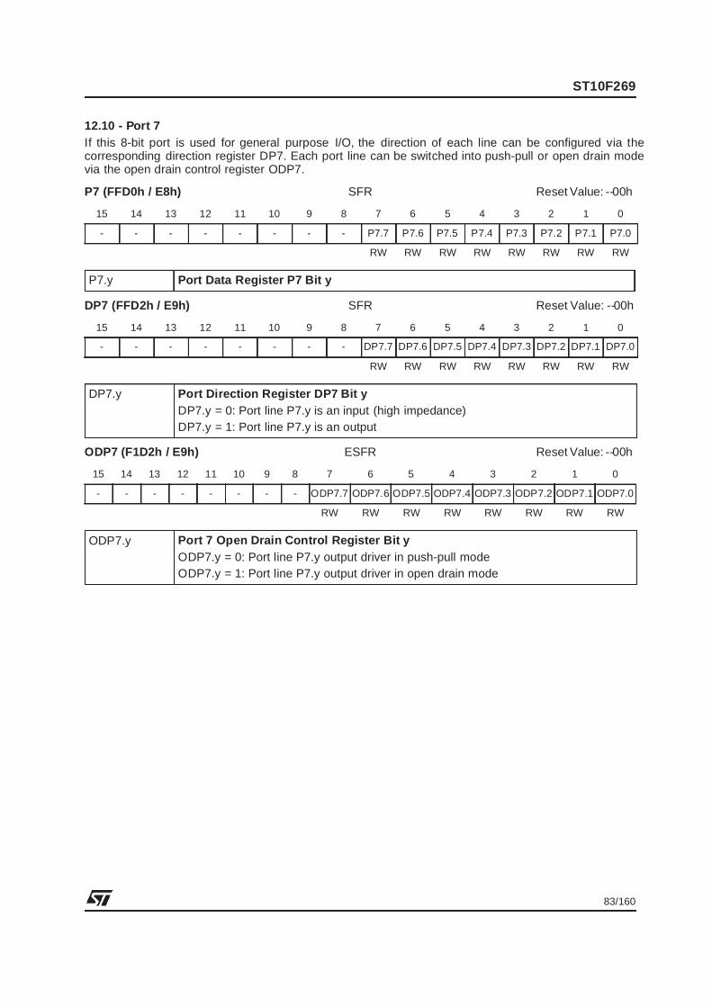
ST10F269
83/160
12.10 - Port 7If this 8-bit port is used for general purpose I/O, the direction of each line can be configured via thecorresponding direction register DP7. Each port line can be switched into push-pull or open drain modevia the open drain control register ODP7.
P7 (FFD0h / E8h) SFR Reset Value: --00h
DP7 (FFD2h / E9h) SFR Reset Value: --00h
ODP7 (F1D2h / E9h) ESFR Reset Value: --00h
15 14 13 12 11 10 9 8 7 6 5 4 3 2 1 0
- - - - - - - - P7.7 P7.6 P7.5 P7.4 P7.3 P7.2 P7.1 P7.0
RW RW RW RW RW RW RW RW
P7.y Port Data Register P7 Bit y
15 14 13 12 11 10 9 8 7 6 5 4 3 2 1 0
- - - - - - - - DP7.7 DP7.6 DP7.5 DP7.4 DP7.3 DP7.2 DP7.1 DP7.0
RW RW RW RW RW RW RW RW
DP7.y Port Direction Register DP7 Bit yDP7.y = 0: Port line P7.y is an input (high impedance)DP7.y = 1: Port line P7.y is an output
15 14 13 12 11 10 9 8 7 6 5 4 3 2 1 0
- - - - - - - - ODP7.7 ODP7.6 ODP7.5 ODP7.4 ODP7.3 ODP7.2 ODP7.1 ODP7.0
RW RW RW RW RW RW RW RW
ODP7.y Port 7 Open Drain Control Register Bit yODP7.y = 0: Port line P7.y output driver in push-pull modeODP7.y = 1: Port line P7.y output driver in open drain mode

ST10F269
84/160
12.10.1 - Alternate Functions of Port 7
The upper 4 lines of Port 7 (P7.7...P7.4) serve ascapture inputs or compare outputs(CC31IO...CC28IO) for the CAPCOM2 unit.
The usage of the port lines by the CAPCOM unit,its accessibility via software and the precautionsare the same as described for the Port 2 lines.
As all other capture inputs, the capture inputfunction of pins P7.7...P7.4 can also be used asexternal interrupt inputs (200ns sample rate at40MHz CPU clock).
The lower 4 lines of Port 7 (P7.3...P7.0) serve asoutputs from the PWM module(POUT3...POUT0).At these pins the value of the respective portoutput latch is EXORed with the value of the PWMoutput rather than ANDed, as the other pins do.This allows to use the alternate output value eitheras it is (port latch holds a `0') or to invert its level atthe pin (port latch holds a `1').Note that the PWM outputs must be enabled viathe respective PENx bit in PWMCON1.The Table 20 summarizes the alternate functionsof Port 7.
Table 20 : Port 7 Alternate Functions
Port 7 Alternate Function
P7.0P7.1P7.2P7.3P7.4P7.5P7.6P7.7
POUT0 PWM mode channel 0 outputPOUT1 PWM mode channel 1 outputPOUT2 PWM mode channel 2 outputPOUT3 PWM mode channel 3 outputCC28IO Capture input / compare output channel 28CC29IO Capture input / compare output channel 29CC30IO Capture input / compare output channel 30CC31IO Capture input / compare output channel 31
Figure 39 : Port 7 I/O and Alternate Functions
Port 7
Alternate FunctionGeneral Purpose Input/Output
P7.7P7.6P7.5P7.4P7.3P7.2P7.1P7.0
CC31IOCC30IOCC29IOCC28IOPOUT3POUT2POUT1POUT0

ST10F269
85/160
The structure of Port 7 differs in the way the outputlatches are connected to the internal bus and tothe pin driver. Pins P7.3...P7.0 (POUT3...POUT0)
EXOR the alternate data output with the port latchoutput, which allows to use the alternate datadirectly or inverted at the pin driver.
Figure 40 : Block Diagram of Port 7 Pins P7.3...P7.0
Open DrainLatch
Write ODP7.y
Read ODP7.y
DirectionLatch
Write DP7.y
Read DP7.y
Inte
rna
lBu
s
MUX
0
1
InputLatch
Clock
P7.y/POUTyOutputBuffer
y = 0...3
Port OutputLatch
Read P7.y
Write DP7.y
=1Port DataOutput
EXOR
AlternateDataOutput

ST10F269
86/160
Figure 41 : Block Diagram of Port 7 Pins P7.7...P7.4
Open DrainLatch
Write ODP7.y
Read ODP7.y
DirectionLatch
Write DP7.y
Read DP7.y
Inte
rnal
Bus
MUX
0
1
Alternate LatchData Input
InputLatch
Clock
P7.yCCzIOOutput
Buffer
AlternateDataOutput
MUX
0
1OutputLatch
. 1Write Port P7.y
Compare Trigger
Read P7.y
y = (4...7)z = (28...31)Alternate Pin
Data Input

ST10F269
87/160
12.11 - Port 8If this 8-bit port is used for general purpose I/O,the direction of each line can be configured via the
corresponding direction register DP8. Each portline can be switched into push/pull or open drainmode via the open drain control register ODP8.
P8 (FFD4h / EAh) SFR ResetValue:--00h
DP8 (FFD6h / EBh) SFR Reset Value: --00h
ODP8 (F1D6h / EBh) ESFR Reset Value: --00h
15 14 13 12 11 10 9 8 7 6 5 4 3 2 1 0
- - - - - - - - P8.7 P8.6 P8.5 P8.4 P8.3 P8.2 P8.1 P8.0
RW RW RW RW RW RW RW RW
P8.y Port Data Register P8 Bit y
15 14 13 12 11 10 9 8 7 6 5 4 3 2 1 0
- - - - - - - - DP8.7 DP8.6 DP8.5 DP8.4 DP8.3 DP8.2 DP8.1 DP8.0
RW RW RW RW RW RW RW RW
DP8.y Port Direction Register DP8 Bit yDP8.y = 0: Port line P8.y is an input (high impedance)DP8.y = 1: Port line P8.y is an output
15 14 13 12 11 10 9 8 7 6 5 4 3 2 1 0
- - - - - - - - ODP8.7 ODP8.6 ODP8.5 ODP8.4 ODP8.3 ODP8.2 ODP8.1 ODP8.0
RW RW RW RW RW RW RW RW
ODP8.y Port 8 Open Drain Control Register Bit yODP8.y = 0: Port line P8.y output driver in push-pull modeODP8.y = 1: Port line P8.y output driver in open drain mode

ST10F269
88/160
12.11.1 - Alternate Functions of Port 8The 8 lines of Port 8 serve as capture inputs or ascompare outputs (CC23IO...CC16IO) for theCAPCOM2 unit.The usage of the port lines by the CAPCOM unit,its accessibility via software and the precautionsare the same as described for the Port 2 lines.
As all other capture inputs, the capture inputfunction of pins P8.7...P8.0 can also be used asexternal interrupt inputs (200ns sample rate at40MHz CPU clock).
The Table 21 summarizes the alternate functionsof Port 8.
Table 21 : Port 8 Alternate Functions
Port 7 Alternate Function
P8.0
P8.1
P8.2
P8.3
P8.4
P8.5
P8.6
P8.7
CC16IO Capture input / compare output channel 16
CC17IO Capture input / compare output channel 17
CC18IO Capture input / compare output channel 18
CC19IO Capture input / compare output channel 19
CC20IO Capture input / compare output channel 20
CC21IO Capture input / compare output channel 21
CC22IO Capture input / compare output channel 22
CC23IO Capture input / compare output channel 23
Figure 42 : Port 8 I/O and Alternate Functions
Port 8
Alternate FunctionGeneral Purpose Input / Output
P8.7P8.6P8.5P8.4P8.3P8.2P8.1P8.0
CC23IOCC22IOCC21IOCC20IOCC19IOCC18IOCC17IOCC16IO

ST10F269
89/160
The structure of Port 8 differs in the way theoutput latches are connected to the internal busand to the pin driver (see Figure 43). Pins
P8.7...P8.0 (CC23IO...CC16IO) combine internalbus data and alternate data output before the portlatch input, as do the Port 2 pins.
Figure 43 : Block Diagram of Port 8 Pins P8.7...P8.0
Open DrainLatch
Write ODP8.y
Read ODP8.y
DirectionLatch
Write DP8.y
Read DP8.y
Inte
rnal
Bus
MUX
0
1
Alternate LatchData Input
InputLatch
Clock
P8.yCCzIOOutput
Buffer
AlternateDataOutput
MUX
0
1OutputLatch
. 1Write Port P8.y
Compare Trigger
Read P8.y
y = (7...0)z = (16...23)Alternate Pin
Data Input

ST10F269
90/160
13 - A/D CONVERTER
A 10-bit A/D converter with 16 multiplexed inputchannels and a sample and hold circuit isintegrated on-chip. The sample time (for loadingthe capacitors) and the conversion time isprogrammable and can be adjusted to theexternal circuitry.To remove high frequency components from theanalog input signal, a low-pass filter must be con-nected at the ADC input.Overrun error detection / protection is controlledby the ADDAT register. Either an interrupt requestis generated when the result of a previousconversion has not been read from the resultregister at the time the next conversion iscomplete, or the next conversion is suspendeduntil the previous result has been read. Forapplications which require less than 16 analoginput channels, the remaining channel inputs canbe used as digital input port pins. The A/Dconverter of the ST10F269 supports differentconversion modes :± Single channel single conversion : the analog
level of the selected channel is sampled onceand converted. The result of the conversion isstored in the ADDAT register.
± Single channel continuous conversion : theanalog level of the selected channel is repeated-ly sampled and converted. The result of the con-version is stored in the ADDAT register.
± Auto scan single conversion : the analog levelof the selected channels are sampled once andconverted. After each conversion the result isstored in the ADDAT register. The data can betransfered to the RAM by interrupt softwaremanagement or using the powerfull PeripheralEvent Controller (PEC) data transfert.
± Auto scan continuous conversion : the ana-log level of the selected channels are repeatedlysampled and converted. The result of the con-version is stored in the ADDAT register. Thedata can be transfered to the RAM by interruptsoftware management or using the PEC datatransfert.
± Wait for ADDAT read mode : when using con-tinuous modes, in order to avoid to overwritethe result of the current conversion by the nextone, the ADWR bit of ADCON control registermust be activated. Then, until the ADDAT regis-ter is read, the new result is stored in a tempo-rary buffer and the conversion is on hold.
± Channel injection mode : when usingcontinuous modes, a selected channel can beconverted in between without changing thecurrent operating mode. The 10-bit data of theconversion are stored in ADRES field ofADDAT2. The current continuous mode remainsactive after the single conversion is completed.
Notes: 1. Section 21.4.5 - Direct Drive for TCL definition.2. tCC = TCL x 24
Table 22 : ADC Sample Clock and Conversion Clock
ADCTC
Conversion Clock t CC
ADSTC
Sample Clock t SC
TCL1 = 1/2 x fXTAL At f CPU = 40MHz tSC = At fCPU = 40MHz
00 TCL x 24 0.3 m s 00 tCC 0.3 m s 2
01 Reserved, do not use Reserved 01 tCC x 2 0.6 m s 2
10 TCL x 96 1.2 m s 10 tCC x 4 1.2 m s 2
11 TCL x 48 0.6 m s 11 tCC x 8 2.4 m s 2

ST10F269
91/160
14 - SERIAL CHANNELS
Serial communication with other microcontrollers,microprocessors, terminals or external peripheralcomponents is provided by two serial interfaces: theasynchronous / synchronous serial channel (ASCO)and the high-speed synchronous serial channel(SSC). Two dedicated Baud rate generators set upall standard Baud rates without the requirement ofoscillator tuning. For transmission, reception anderroneous reception, 3 separate interrupt vectorsare provided for each serial channel.
14.1 - Asynchronous / Synchronous SerialInterface (ASCO)The asynchronous / synchronous serial interface(ASCO) provides serial communication betweenthe ST10F269 and other microcontrollers,microprocessors or external peripherals.A set of registers is used to configure and tocontrol the ASCO serial interface:± P3, DP3, ODP3 for pin configuration
± SOBG for Baud rate generator
± SOTBUF for transmit buffer
± SOTIC for transmit interrupt control
± SOTBIC for transmit buffer interrupt control
± SOCON for control
± SORBUF for receive buffer (read only)
± SORIC for receive interrupt control
± SOEIC for error interrupt control
14.1.1 - ASCO in Asynchronous Mode
In asynchronous mode, 8 or 9-bit data transfer,parity generation and the number of stop bit canbe selected. Parity framing and overrun errordetection is provided to increase the reliability ofdata transfers. Transmission and reception of datais double-buffered. Full-duplex communication upto 1.25M Bauds (at 40MHz of fCPU) is supportedin this mode.
Figure 44 : Asynchronous Mode of Serial Channel ASC0
Pin
2CPUClock
S0R
Baud RateTimer
ReloadRegister
16
Clock
Serial Port Control
Shift Clock
S0M S0STP S0FE S0OES0PE
S0REN
S0FEN
S0PEN
S0OEN
S0LB
S0RIR
S0TIR
S0EIR
Receive InterruptRequest
Transmit InterruptRequest
Error InterruptRequest
Transmit ShiftRegister
Receive ShiftRegister
TXD0 / P3.10
Transmit BufferRegister S0TBUF
Receive BufferRegister S0RBUF
SamplingMUX0
1
Pin
Input
Internal Bus
RXD0/P3.11
Output

ST10F269
92/160
Asynchronous Mode Baud ratesFor asynchronous operation, the Baud rategenerator provides a clock with 16 times the rateof the established Baud rate. Every received bit issampled at the 7th, 8th and 9th cycle of this clock.The Baud rate for asynchronous operation ofserial channel ASC0 and the required reloadvalue for a given Baud rate can be determined bythe following formulas:(S0BRL) represents the content of the reloadregister, taken as unsigned 13-bit integer,(S0BRS) represents the value of bit S0BRS (`0' or`1'), taken as integer.
Using the above equation, the maximum Baudrate can be calculated for any given clock speed.Baud rate versus reload register value (SOBRS=0and SOBRS=1) is described in Table 23.
Note: The deviation errors given in the Table 23 are rounded. To avoid deviation errors use a Baud ratecrystal (providing a multiple of the ASC0/SSC sampling frequency).
BAsync =fCPU
16 x [2 + (S0BRS)] x [(S0BRL) + 1]
S0BRL = (fCPU
16 x [2 + (S0BRS)] x BAsync) - 1
Table 23 : Commonly Used Baud Rates by Reload Value and Deviation Errors
S0BRS = `0', f CPU = 40MHz S0BRS = `1', fCPU = 40MHz
Baud Rate (Baud) Deviation ErrorReload Value
(hexa)Baud Rate (Baud) Deviation Error
Reload Value(hexa)
1 250 000 0.0% / 0.0% 0000 / 0000 833 333 0.0% / 0.0% 0000 / 0000
112 000 +1.5% / -7.0% 000A / 000B 112 000 +6.3% / -7.0% 0006 / 0007
56 000 +1.5% / -3.0% 0015 / 0016 56 000 +6.3% / -0.8% 000D / 000E
38 400 +1.7% / -1.4% 001F / 0020 38 400 +3.3% / -1.4% 0014 / 0015
19 200 +0.2% / -1.4% 0040 / 0041 19 200 +0.9% / -1.4% 002A / 002B
9 600 +0.2% / -0.6% 0081 / 0082 9 600 +0.9% / -0.2% 0055 / 0056
4 800 +0.2% / -0.2% 0103 / 0104 4 800 +0.4% / -0.2% 00AC / 00AD
2 400 +0.2% / -0.0% 0207 / 0208 2 400 +0.1% / -0.2% 015A / 015B
1 200 0.1% / 0.0% 0410 / 0411 1 200 +0.1% / -0.1% 02B5 / 02B6
600 0.0% / 0.0% 0822 / 0823 600 +0.1% / -0.0% 056B / 056C
300 0.0% / 0.0% 1045 / 1046 300 0.0% / 0.0% 0AD8 / 0AD9
153 0.0% / 0.0% 1FE8 / 1FE9 102 0.0% / 0.0% 1FE8 / 1FE9

ST10F269
93/160
14.1.2 - ASCO in Synchronous ModeIn synchronous mode, data are transmitted or received synchronously to a shift clock which is generatedby the ST10F269. Half-duplex communication up to 5M Baud (at 40MHz of fCPU) is possible in this mode.
Figure 45 : Synchronous Mode of Serial Channel ASC0
2CPUClock
S0R
Baud Rate Timer
Reload Register
4
Clock
Serial Port Control
Shift Clock
S0M = 000B S0OE
S0REN
S0OEN
S0LB
S0RIR
S0TIR
S0EIR
Receive InterruptRequest
Transmit InterruptRequest
Error InterruptRequest
Transmit ShiftRegister
Receive ShiftRegister
Transmit BufferRegisterS0TBUF
Receive BufferRegisterS0RBUF
MUX0
1
Pin
Internal Bus
Receive
Output
Transmit
Pin
Input/Output
TDX0/P3.10
RXD0/P3.11

ST10F269
94/160
Synchronous Mode Baud RatesFor synchronous operation, the Baud rategenerator provides a clock with 4 times the rate ofthe established Baud rate. The Baud rate forsynchronous operation of serial channel ASC0can be determined by the following formula:(S0BRL) represents the content of the reloadregister, taken as unsigned 13-bit integers,(S0BRS) represents the value of bit S0BRS (`0' or`1'), taken as integer.
Using the above equation, the maximum Baudrate can be calculated for any clock speed asgiven in Table 24.
Note: The deviation errors given in the Table 24 are rounded. To avoid deviation errors use a Baud ratecrystal (providing a multiple of the ASC0/SSC sampling frequency)
BSync =
S0BRL = (fCPU
4 x [2 + (S0BRS)] x BSync) - 1
fCPU
4 x [2 + (S0BRS)] x [(S0BRL) + 1]
Table 24 : Commonly Used Baud Rates by Reload Value and Deviation Errors
S0BRS = `0', f CPU = 40MHz S0BRS = `1', fCPU = 40MHz
Baud Rate (Baud) Deviation ErrorReload Value
(hexa)Baud Rate (Baud) Deviation Error
Reload Value(hexa)
5 000 000 0.0% / 0.0% 0000 / 0000 3 333 333 0.0% / 0.0% 0000 / 0000
112 000 +1.5% / -0.8% 002B / 002C 112 000 +2.6% / -0.8% 001C / 001D
56 000 +0.3% / -0.8% 0058 / 0059 56 000 +0.9% / -0.8% 003A / 003B
38 400 +0.2% / -0.6% 0081 / 0082 38 400 +0.9% / -0.2% 0055 / 0056
19 200 +0.2% / -0.2% 0103 / 0104 19 200 +0.4% / -0.2% 00AC / 00AD
9 600 +0.2% / -0.0% 0207 / 0208 9 600 +0.1% / -0.2% 015A / 015B
4 800 +0.1% / -0.0% 0410 / 0411 4 800 +0.1% / -0.1% 02B5 / 02B6
2 400 0.0% / 0.0% 0822 / 0823 2 400 +0.1% / -0.0% 056B / 056C
1 200 0.0% / 0.0% 1045 / 1046 1 200 0.0% / 0.0% 0AD8 / 0AD9
900 0.0% / 0.0% 15B2 / 15B3 600 0.0% / 0.0% 15B2 / 15B3
612 0.0% / 0.0% 1FE8 / 1FE9 407 0.0% / 0.0% 1FFD / 1FFE
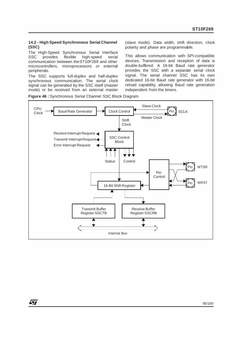
ST10F269
95/160
14.2 - High Speed Synchronous Serial Channel(SSC)The High-Speed Synchronous Serial InterfaceSSC provides flexible high-speed serialcommunication between theST10F269 and othermicrocontrollers, microprocessors or externalperipherals.The SSC supports full-duplex and half-duplexsynchronous communication. The serial clocksignal can be generated by the SSC itself (mastermode) or be received from an external master
(slave mode). Data width, shift direction, clockpolarity and phase are programmable.
This allows communication with SPI-compatibledevices. Transmission and reception of data isdouble-buffered. A 16-bit Baud rate generatorprovides the SSC with a separate serial clocksignal. The serial channel SSC has its owndedicated 16-bit Baud rate generator with 16-bitreload capability, allowing Baud rate generationindependent from the timers.
Figure 46 : Synchronous Serial Channel SSC Block Diagram
Baud Rate Generator
SSC ControlBlock
Pin
Internal Bus
Clock ControlCPUClock
Slave Clock
Master Clock
SCLK
ShiftClock
Status Control
Receive Interrupt Request
Transmit Interrupt Request
Error Interrupt Request
16-Bit Shift Register
PinControl
Pin
Pin
MTSR
MRST
Transmit BufferRegister SSCTB
Receive BufferRegister SSCRB

ST10F269
96/160
Baud Rate Generation
The Baud rate generator is clocked by fCPU/2. Thetimer is counting downwards and can be startedor stopped through the global enable bit SSCENin register SSCCON. Register SSCBR is thedual-function Baud Rate Generator/Reloadregister. Reading SSCBR, while the SSC isenabled, returns the content of the timer. ReadingSSCBR, while the SSC is disabled, returns theprogrammed reload value. In this mode thedesired reload value can be written to SSCBR.
Note Never write to SSCBR, while the SSC isenabled.
The formulas below calculate the resulting Baudrate for a given reload value and the requiredreload value for a given Baud rate:
(SSCBR) represents the content of the reloadregister, taken as unsigned 16-bit integer.
Table 25 lists some possible Baud rates againstthe required reload values and the resulting bittimes for a 40MHz CPU clock.
Baud rateSSC =fCPU
2 x [(SSCBR) + 1]
SSCBR = (fCPU
2 x Baud rateSSC) - 1
Table 25 : Synchronous Baud Rate and ReloadValues
Baud Rate Bit Time Reload Value
Reserved use areload value > 0.
--- ---
10M Baud 100ns 0001h
5M Baud 200ns 0003h
2.5M Baud 400ns 0007h
1M Baud 1m s 0013h
100K Baud 10 m s 00C7h
10K Baud 100 m s 07CFh
1K Baud 1ms 4E1Fh
306 Baud 3.26ms FF4Eh

ST10F269
97/160
15 - CAN MODULES
The two integrated CAN modules (CAN1 andCAN2) are identical and handle the completelyautonomous transmission and reception of CANframes according to the CAN specification V2.0part B (active).Each on-chip CAN module can receive andtransmit standard frames with 11-bit identifiers aswell as extended frames with 29-bit identifiers.These two CAN modules are both identical to theCAN module of the ST10F167.Because of duplication of the CAN controllers, thefollowing adjustments are to be considered:
± Same internal register addresses of both CANcontrollers, but with base addresses differing inaddress bit A8; separate chip select for eachCAN module. Refer to Chapter 4 - Memory Or-ganization.
± The CAN1 transmit line (CAN1_TxD) is thealternate function of the Port P4.6 pin and thereceive line (CAN1_RxD) is the alternatefunction of the Port P4.5 pin.
± The CAN2 transmit line (CAN2_TxD) is thealternate function of the Port P4.7 pin and thereceive line (CAN2_RxD) is the alternatefunction of the Port P4.4 pin.
± Interrupt request line of the CAN1 module isconnected to the XBUS interrupt line XP0,interrupt of the CAN2 module is connected tothe line XP1.
± The CAN modules must be selected withcorresponding CANxEN bit of XPERCON registerbefore the bit XPEN of SYSCON register is set.
± The reset default configuration is : CAN1 isenabled, CAN2 is disabled.
15.1 - CAN Modules Memory Mapping
15.1.1 - CAN1Address range 00'EF00h - 00'EFFFh is reservedfor the CAN1 Module access. CAN1 is enabled bysetting XPEN bit 2 of the SYSCON register and bysetting bit 0 of the XPERCON register. Accessesto the CAN Module use demultiplexed addressesand a 16-bit data bus (Byte accesses arepossible). Two wait states give an access time of125ns at 40MHz CPU clock. No tri-state waitstates are used.
15.1.2 - CAN2
Address range 00'EE00h - 00'EEFFh is reservedfor the CAN2 Module access. CAN2 is enabled bysetting XPEN bit 2 of the SYSCON register and bysetting bit 1 of the XPERCON register. Accessesto the CAN Module use demultiplexed addressesand a 16-bit data bus (Byte accesses arepossible). Two wait states give an access time of125ns at 40MHz CPU clock. No tri-state waitstates are used.
Note: If one or both CAN modules is used,Port 4 cannot be programmed to output all8 segment address lines. Thus, only4 segment address lines can be used,reducing the external memory space to5M Bytes (1M Byte perCS line).
15.2 - CAN Bus Configurations
Depending on application, CAN bus configurationmay be one single bus with a single or multipleinterfaces or a multiple bus with a single ormultiple interfaces. The ST10F269 is able tosupport these 2 cases.
Single CAN Bus
The single CAN Bus multiple interfacesconfiguration may be implemented using 2 CANtransceives as shown in Figure 47.Figure 47 : Single CAN Bus Multiple Interfaces,Multiple Transceivers
CAN1RxD TxD
CAN2RxD TxD
CANTransceiver
CANTransceiver
CAN_H
CAN_H CAN bus

ST10F269
98/160
The ST10F269 also supports single CAN Busmultiple (dual) interfaces using the open drainoption of the CANx_TxD output as shown inFigure 48. Thanks to the OR-Wired Connection,only one transceiver is required. In this case thedesign of the application must take in account thewire length and the noise environment.
Multiple CAN Bus
The ST10F269 provides 2 CAN interfaces tosupport such kind of bus configuration as shownin Figure 49.
Figure 48 : Single CAN Bus, Dual Interfaces,Single Transceiver
CAN1RxD TxD
CAN2RxD TxD
CANTransceiver
CAN_H
CAN_H CAN bus
* Open drain output
+5V
2.7kW
* *
Figure 49 : Connection to Two Different CANBuses (e.g. for gateway application)
CAN1RxD TxD
CAN2RxD TxD
CANTransceiver
CANTransceiver
CAN_H
CAN_H CANCANbus 2bus 1
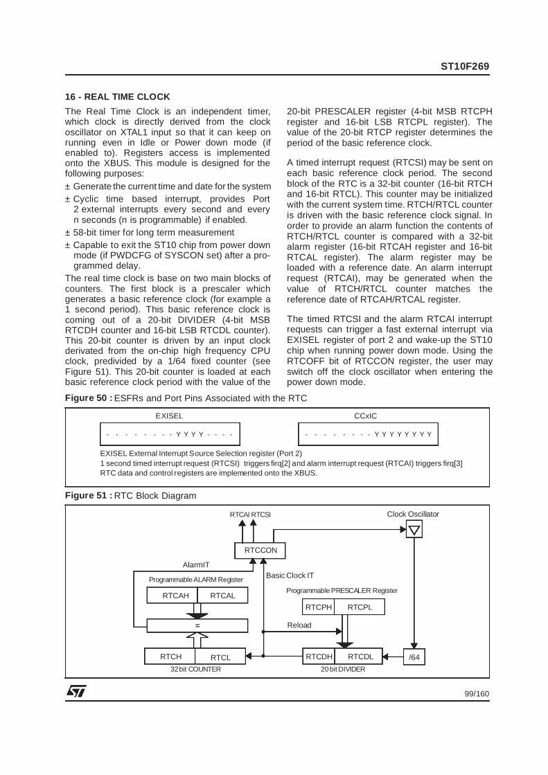
ST10F269
99/160
16 - REAL TIME CLOCK
The Real Time Clock is an independent timer,which clock is directly derived from the clockoscillator on XTAL1 input so that it can keep onrunning even in Idle or Power down mode (ifenabled to). Registers access is implementedonto the XBUS. This module is designed for thefollowing purposes:± Generate the current time and date for the system± Cyclic time based interrupt, provides Port
2 external interrupts every second and everyn seconds (n is programmable) if enabled.
± 58-bit timer for long term measurement± Capable to exit the ST10 chip from power down
mode (if PWDCFG of SYSCON set) after a pro-grammed delay.
The real time clock is base on two main blocks ofcounters. The first block is a prescaler whichgenerates a basic reference clock (for example a1 second period). This basic reference clock iscoming out of a 20-bit DIVIDER (4-bit MSBRTCDH counter and 16-bit LSB RTCDL counter).This 20-bit counter is driven by an input clockderivated from the on-chip high frequency CPUclock, predivided by a 1/64 fixed counter (seeFigure 51). This 20-bit counter is loaded at eachbasic reference clock period with the value of the
20-bit PRESCALER register (4-bit MSB RTCPHregister and 16-bit LSB RTCPL register). Thevalue of the 20-bit RTCP register determines theperiod of the basic reference clock.
A timed interrupt request (RTCSI) may be sent oneach basic reference clock period. The secondblock of the RTC is a 32-bit counter (16-bit RTCHand 16-bit RTCL). This counter may be initializedwith the current system time. RTCH/RTCL counteris driven with the basic reference clock signal. Inorder to provide an alarm function the contents ofRTCH/RTCL counter is compared with a 32-bitalarm register (16-bit RTCAH register and 16-bitRTCAL register). The alarm register may beloaded with a reference date. An alarm interruptrequest (RTCAI), may be generated when thevalue of RTCH/RTCL counter matches thereference date of RTCAH/RTCAL register.
The timed RTCSI and the alarm RTCAI interruptrequests can trigger a fast external interrupt viaEXISEL register of port 2 and wake-up the ST10chip when running power down mode. Using theRTCOFF bit of RTCCON register, the user mayswitch off the clock oscillator when entering thepower down mode.
Figure 50 : ESFRs and Port Pins Associated with the RTC
Figure 51 : RTC Block Diagram
- - - - - - - - Y Y Y Y - - - -
EXISEL
EXISEL External Interrupt Source Selection register (Port 2)1 second timed interrupt request (RTCSI) triggers firq[2] and alarm interrupt request (RTCAI) triggers firq[3]RTC data and control registers are implemented onto the XBUS.
- - - - - - - - Y Y Y Y Y Y Y Y
CCxIC
/64
RTCPLRTCPH
RTCH RTCL RTCDH RTCDL
RTCAH RTCAL
Clock Oscillator
Reload=
20 bit DIVIDER32bit COUNTER
RTCCON
AlarmITBasic Clock IT
RTCAI RTCSI
ProgrammableALARM Register
Programmable PRESCALER Register

ST10F269
100/160
16.1 - RTC registers
16.1.1 - RTCCON: RTC Control RegisterThe functions of the RTC are controlled by the RTCCON control register. If the RTOFF bit is set, the RTCdividers and counters clock is disabled and registers can be written, when the ST10 chip enters powerdown mode the clock oscillator will be switch off. The RTC has 2 interrupt sources, one is triggered everybasic clock period, the other one is the alarm.RTCCON includes an interrupt request flag and an interrupt enable bit for each of them. This register isread and written via the XBUS.
RTCCON (EC00h) XBUS Reset Value:--00h
Notes: 1. As RTCCON register is not bit-addressable, the value of these bits must be read by checking their associated CCxIC register.The 2 RTC interrupt signals are connected to Port2 in order to trigger an external interrupt that wake up the chip when in power downmode.2. All the bit of RTCCON are active high.
15 14 13 12 11 10 9 8 7 6 5 4 3 2 1 0
- - - - - - - - RTCOFF - - - RTCAEN RTCAIR RTCSEN RTCSIR
RW RW RW RW RW
RTCOFF 2 RTC Switch Off Bit`0': clock oscillator and RTC keep on running even if ST10 in power down mode`1': clock oscillator is switch off if ST10 enters power down mode, RTC dividers andcounters are stopped and registers can be written
RTCAEN 2 RTC Alarm Interrupt ENable`0': RTCAI is disabled`1': RTCAI is enabled, it is generated every n seconds
RTCAIR 1 RTC Alarm Interrupt Request flag (when the alarm is triggered)`0': the bit was reseted less than a n seconds ago`1': the interrupt was triggered
RTCSEN 2 RTC Second interrupt ENable`0': RTCSI is disabled`1': RTCSI is enabled, it is generated every second
RTCSIR 1 RTC Second Interrupt Request flag (every second)`0': the bit was reseted less than a second ago`1': the interrupt was triggered

ST10F269
101/160
16.1.2 - RTCPH & RTCPL: RTC PRESCALER Registers
The 20-bit programmable prescaler divider is loaded with 2 registers.
The 4 most significant bit are stored into RTCPH and the 16 Less significant bit are stored in RTCPL. Inorder to keep the system clock, those registers are not reset.
They are write protected by bit RTOFF of RTCCON register, write operation is allowed if RTOFF is set.
RTCPL (EC06h) XBUS Reset Value: XXXXh
RTCPH (EC08h) XBUS Reset Value: ---Xh
The value stored into RTCPH, RTCPL is called RTCP (coded on 20-bit). The dividing ratio of theprescalar divider is: ratio = 64 x (RTCP)
16.1.3 - RTCDH & RTCDL: RTC DIVIDER Counters
Every basic reference clock the DIVIDER counters are reloaded with the value stored RTCPH andRTCPL registers. To get an accurate time measurement it is possible to read the value of the DIVIDER,reading the RTCDH, RTCDL. Those counters are read only. After any bit changed in the programmablePRESCALER register, the new value is loaded in the DIVIDER.
RTCDL (EC0Ah) XBUS Reset Value: XXXXh
RTCDH (EC0Ch) XBUS Reset Value: ---Xh
Note: Those registers are not reset, and are read only.
15 14 13 12 11 10 9 8 7 6 5 4 3 2 1 0
RTCPL
RW
15 14 13 12 11 10 9 8 7 6 5 4 3 2 1 0
RESERVED RTCPH
RW
Figure 52 : PRESCALER Register
15 14 13 12 11 10 9 8 7 6 5 4 3 2 1 0
RTCDL
R
15 14 13 12 11 10 9 8 7 6 5 4 3 2 1 0
RESERVED RTCDH
R
3 2 1 07 6 5 411 10 9 815 14 13 123 2 1 0
RTCPH RTCPL
3 2 1 07 6 5 411 10 9 815 14 13 1219 18 17 16
20 bit word counter

ST10F269
102/160
When RTCD increments to reach 00000h, The 20-bit word stored into RTCPH, RTCPL registers is loadedin RTCD.
Bit 15 to bit 4 of RTCPH and RTCDH are not used. When reading, the return value of those bit will bezeros.
16.1.4 - RTCH & RTCL: RTC Programmable COUNTER RegistersThe RTC has 2 x 16-bit programmable counters which count rate is based on the basic time reference (forexample 1 second). As the clock oscillator may be kept working, even in power down mode, the RTCcounters may be used as a system clock. In addition RTC counters and registers are not modified at anysystem reset. The only way to force their value is to write them via the XBUS.Those counters are write protected as well. The bit RTOFF of the RTCCON register must be set (RTCdividers and counters are stopped) to enable a write operation on RTCH or RTCL.A write operation on RTCH or RTCL register loads directly the corresponding counter. When reading, thecurrent value in the counter (system date) is returned.The counters keeps on running while the clock oscillator is working.
RTCL (EC0Eh) XBUS Reset Value: XXXXh
RTCH (EC10h) XBUS Reset Value: XXXXh
Note: Those registers are nor reset
Figure 53 : DIVIDER Counters
15 14 13 12 11 10 9 8 7 6 5 4 3 2 1 0
RTCL
RW
15 14 13 12 11 10 9 8 7 6 5 4 3 2 1 0
RTCH
RW
3 2 1 07 6 5 411 10 9 815 14 13 123 2 1 0
RTCDH RTCDL
3 2 1 07 6 5 411 10 9 815 14 13 1219 18 17 16
20 bit word internal value of the prescalardivider

ST10F269
103/160
16.1.5 - RTCAH & RTCAL: RTC ALARM Registers
When the programmable counters reach the 32-bit value stored into RTCAH & RTCAL registers, an alarmis triggered and the interrupt request RTAIR is generated. Those registers are not protected.
RTCAL (EC12h) XBUS Reset Value: XXXXh
RTCAH (EC14h) XBUS Reset Value: XXXXh
Note: Those registers are not reset
16.2 - Programming the RTC
RTC interrupt request signals are connected to Port2, pad 10 (RTCSI) and pad 11 (RTCAI). An alternatefunction Port2 is to generate fast interrupts firq[7:0]. To trigger firq[2] and firq[3] the following configurationhas to be set.
EXICON ESFR controls the external interrupt edge selection, RTC interrupt requests are rising edgeactive.
EXICON (F1C0h) ESFR Reset Value: 0000h
Notes: 1. EXI2ES and EXI3ES must be configured as º01bº because RCT interrupt request lines are rising edge active.2. Alarm interrupt request line (RTCAI) is linked with EXI3ES.3. Timed interrupt request line (RTCSI) is linked with EXI2ES.
EXISEL ESFR enables the Port2 alternate sources. RTC interrupts are alternate sources 2 and 3.
EXISEL (F1DAh) ESFR Reset Value: 0000h
Notes: 1. Advised configuration.2. Alarm interrupt request (RTCAI) is linked with EXI3SS.3. Timed interrupt request (RTCSI) is linked with EXI2SS.
15 14 13 12 11 10 9 8 7 6 5 4 3 2 1 0
RTCAL
RW
15 14 13 12 11 10 9 8 7 6 5 4 3 2 1 0
RTCAH
RW
15 14 13 12 11 10 9 8 7 6 5 4 3 2 1 0
EXI7ES EXI6ES EXI5ES EXI4ES EXI3ES 1 2 EXI2ES 1 3 EXI1ES EXI0ES
RW RW RW RW RW RW RW RW
15 14 13 12 11 10 9 8 7 6 5 4 3 2 1 0
EXI7SS EXI6SS EXI5SS EXI4SS EXI3SS 2 EXI2SS 3 EXI1SS EXI0SS
RW RW RW RW RW RW RW RW
EXIxSS External Interrupt x Source Selection (x=7...0)`00': Input from associated Port 2 pin.`01': Input from ªalternate sourceº.1
`10': Input from Port 2 pin ORed with ªalternate sourceº. 1
`11': Input from Port 2 pin ANDed with ªalternate sourceº.

ST10F269
104/160
Interrupt control registers are common with CAPCOM1 Unit: CC10IC (RTCSI) and CC11IC (RTCAI).
CCxIC SFR Reset Value: --00h
CC10IC: FF8Ch/C6hCC11IC: FF8Eh/C7h
15 14 13 12 11 10 9 8 7 6 5 4 3 2 1 0
- - - - - - - - CCxIR CCxIE ILVL GLVL
RW RW RW RW
Source of interrupt Request Flag Enable Flag Interrupt Vector Vector Location Trap Number
External interrupt 2 CC10IR CC10IE CC10INT 00'0068h 1Ah/26
External interrupt 3 CC11IR CC11IE CC11INT 00'006Ch 1Bh/27

ST10F269
105/160
17 - WATCHDOG TIMER
The Watchdog Timer is a fail-safe mechanism which prevents the microcontroller from malfunctioning forlong periods of time.The Watchdog Timer is always enabled after a reset of the chip and can only be disabled in the timeinterval until the EINIT (end of initialization) instruction has been executed.Therefore, the chip start-up procedure is always monitored. The software must be designed to service thewatchdog timer before it overflows. If, due to hardware or software related failures, the software fails to doso, the watchdog timer overflows and generates an internal hardware reset. It pulls theRSTOUT pin lowin order to allow external hardware components to be reset.Each of the different reset sources is indicated in the WDTCON register.The indicated bits are cleared with the EINIT instruction. The origine of the reset can be identified duringthe initialization phase.
WDTCON (FFAEh / D7h) SFR Reset Value: 00xxh
Notes: 1. More than one reset indication flag may be set. After EINIT,all flags are cleared.2. Power-on is detected when a rising edge from VDD = 0 V to VDD > 2.0 V is recognized on the internal 3.3V supply.
3. These bits cannot be directly modified by software.
15 14 13 12 11 10 9 8 7 6 5 4 3 2 1 0
WDTREL - - PONR LHWR SHWR SWR WDTR WDTIN
RW HR HR HR HR HR RW
WDTIN Watchdog Timer Input Frequency Selection
`0': Input Frequency is fCPU/2.
`1': Input Frequency is fCPU/128.
WDTR1-3 Watchdog Timer Reset Indication Flag
Set by the watchdog timer on an overflow.
Cleared by a hardware reset or by the SRVWDT instruction.
SWR1-3 Software Reset Indication Flag
Set by the SRST execution.
Cleared by the EINIT instruction.
SHWR1-3 Short Hardware Reset Indication Flag
Set by the input RSTIN.
Cleared by the EINIT instruction.
LHWR1-3 Long Hardware Reset Indication Flag
Set by the input RSTIN.
Cleared by the EINIT instruction.
PONR1- 2-3 Power-On (Asynchronous) Reset Indication Flag
Set by the input RSTIN if a power-on condition has been detected.
Cleared by the EINIT instruction.

ST10F269
106/160
The PONR flag of WDTCON register is set if the output voltage of the internal 3.3V supply falls below thethreshold (typically 2V) of the power-on detection circuit. This circuit is efficient to detect major failures ofthe external 5V supply but if the internal 3.3V supply does not drop under 2 volts, the PONR flag is notset. This could be the case on fast switch-off / switch-on of the 5V supply. The time needed for such asequence to activate the PONR flag depends on the value of the capacitors connected to the supply andon the exact value of the internal threshold of the detection circuit.
Notes: 1. PONR bit may not be set for short supply failure.
2. For power-on reset and reset after supply partial failure, asynchronous reset must be used.
In case of bi-directional reset is enabled, and if theRSTIN pin is latched low after the end of the internalreset sequence, then a Short hardware reset, a software reset or a watchdog reset will trigger a Longhardware reset. Thus, Reset Indications flags will be set to indicate a Long Hardware Reset.The Watchdog Timer is 16-bit, clocked with the system clock divided by 2 or 128. The high Byte of thewatchdog timer register can be set to a pre-specified reload value (stored in WDTREL).Each time it is serviced by the application software, the high byte of the watchdog timer is reloaded. Forsecurity, rewrite WDTCON each time before the watchdog timer is servicedThe Table 27 shows the watchdog time range for 40MHz CPU clock.
The watchdog timer period is calculated with the following formula:
Table 26 : WDTCON Bit Value on Different Resets
Reset Source PONR LHWR SHWR SWR WDTR
Power On Reset X X X X
Power on after partial supply failure 1) 2) X X X
Long Hardware Reset X X X
Short Hardware Reset X X
Software Reset X
Watchdog Reset X X
Table 27 : WDTREL Reload Value
Reload value in WDTRELPrescaler for f CPU = 40MHz
2 (WDTIN = `0') 128 (WDTIN = `1')
FFh 12.8 m s 819.2ms
00h 3.276ms 209.7ms
PWDT1
fCPU--------------- 512ψ 1 WDTIN] 63 ) 256 WDTREL] )[±(ψψ[+(ψ=

ST10F269
107/160
18 - SYSTEM RESET
System reset initializes the MCU in a predefined state. There are five ways to activate a reset state. Thesystem start-up configuration is different for each case as shown in Table 28.
Table 28 : Reset Event Definition
18.1 - Long Hardware Reset
The reset is triggered when RSTIN pin is pulled low, then the MCU is immediately forced in reset defaultstate. It pulls low RSTOUT pin, it cancels pending internal hold states if any, it aborts external bus cycle, itswitches buses (data, address and control signals) and I/O pin drivers to high-impedance, it pulls high PORT0pins and the reset sequence starts.
To get a long hardware reset , the duration of the externalRSTIN signal must be longer than1040 TCL.The level of RPD pin is sampled during the wholeRSTIN pulse duration. A low level on RPD pindetermines an asynchronous reset while a high level leads to a synchronous reset .
Note A reset can be entered as synchronous and exit as asynchronous if VRPD voltage drops below theRPD pin threshold (typically 2.5V for VDD = 5V) when RSTIN pin is low or when RSTIN pin isinternally pulled low.
18.1.1 - Asynchronous Reset
Figure 54 and Figure 55 showasynchronous reset condition (RPD pin is at low level) .
Figure 54 : Asynchronous Reset Sequence External Fetch
Note: 1) RSTIN rising edge to internal latch of PORT0 is 3 CPU clock cycles (6 TCL) if the PLL is bypassed and the prescaler is on(fCPU = fXTAL / 2), else it is 4 CPU clock cycles (8 TCL).
Reset Source Short-cut Conditio ns
Power-on reset PONR Power-on
Long Hardware reset (synchronous & asynchronous) LHWR t RSTIN > 1040 TCL
Short Hardware reset (synchronous reset) SHWR 4 TCL < t RSTIN < 1038 TCL
Watchdog Timer reset WDTR WDT overflowSoftware reset SWR SRST execution
6 or 8 TCL1)
CPU Clock
RSTINAsynchronous
Reset Condition
RPD
RSTOUT
ALE
PORT0 Reset Configuration 1st Instruction External Fetch
Latching point of PORT0for system start-upconfiguration
81 2 3 4 6 75 9
RD
EXTERNAL FETCHInternal reset
5 TCL

ST10F269
108/160
Figure 55 : Asynchronous Reset Sequence Internal Fetch
Note: 1) RSTIN rising edge to internal latch of PORT0 is 3 CPU clock cycles (6 TCL) if the PLL is bypassed and the prescaler is on(fCPU = fXTAL / 2), else it is 4 CPU clock cycles (8 TCL).
2) 2.1m s typical value.
Power-on resetThe asynchronous reset must be used during the power-on of the MCU. Depending on the crystal frequency,the on-chip oscillator needs about 10ms to 50ms to stabilize. The logic of the MCU does not need a stabilizedclock signal to detect an asynchronous reset, so it is suitable for power-on conditions. To ensure a properreset sequence, the RSTIN pin and the RPD pin must be held at low level until the MCU clock signal isstabilized and the system configuration value on PORT0 is settled.Hardware resetThe asynchronous reset must be used to recover from catastrophic situations of the application. It may betriggerred by the hardware of the application . Internal hardware logic and application circuitry aredescribed in Section 18.6 -Reset Circuitry and Figure 58, Figure 59 and Figure 60.
18.1.2 - Synchronous Reset ( RSTIN pulse > 1040TCL and RPD pin at high level)The synchronous reset is a warm reset. It may be generated synchronously to the CPU clock. To bedetected by the reset logic, theRSTIN pulse must be low at least for 4 TCL (2 periods of CPU clock).Then the I/O pins are set to high impedance andRSTOUT pin is driven low. After the RSTIN level isdetected, a short duration of 12 TCL (6 CPU clocks) maximum elapses, during which pending internalhold states are cancelled and the current internal access cycle, if any, is completed. External bus cycle isaborted.The internal pull-down of RSTIN pin is activated if bit BDRSTEN of SYSCON register was previously set
by software. This bit is always cleared on power-on or after any reset sequence.The internal sequence lasts for 1024 TCL (512 periods of CPU clock). After this duration the pull-down ofRSTIN pin for the bidirectional reset function is released and theRSTIN pin level is sampled. At this stepthe sequence lasts 1040 TCL (4 TCL + 12 TCL + 1024 TCL). If the RSTIN pin level is low, the resetsequence is extended untilRSTIN level becomes high. Refer to Figure 56Note If VRPD voltage drops below the RPD pin threshold (typically 2.5V for VDD = 5V) when RSTIN pin
is low or whenRSTIN pin is internally pulled low, the ST10 reset circuitry disables the bidirectionalreset function and RSTIN pin is no more pulled low. The reset is processed as an asynchronousreset.
6 or 8 TCL 1)
CPU Clock
RSTIN
AsynchronousReset Condition
RPD
RSTOUT
PORT0 Reset Configuration
INTERNAL FETCH
Internal reset signal
Flash read signal
PLL factorlatch command
Flashunder reset for internal charge pump ramping up
1st fetchfrom Flash
Latching point of PORT0for PLL configuration
Latching point of PORT0for remaining bits
1 2 3
2.5m s max.2)

ST10F269
109/160
Figure 56 : Synchronous Reset Sequence External Fetch (RSTIN pulse > 1040 TCL)
Note 1) RSTIN rising edge to internal latch of PORT0 is 3 CPU clock cycles (6 TCL) if the PLL is bypassed and the prescaler is on(fCPU = fXTAL / 2), else it is 4 CPU clock cycles (8 TCL).
2) RSTIN pin is pulled low if bit BDRSTEN (bit 3 of SYSCON register) was previously set by software. Bit BDRSTEN is cleared afterreset.
3) If during the reset condition (RSTIN low), VRPD voltage drops below the threshold voltage (typically 2.5V for 5V operation), the theST10 reset circuitry disables the bidirectional reset function and RSTIN pin is no more pulled low.
18.1.3 - Exit of Long Hardware Reset- If the RPD pin level is low when the RSTIN pin is sampled high , the MCU completes anasynchronous reset sequence.- If the RPD pin level is high when the RSTIN pin is sampled high , the MCU completes asynchronous reset sequence.The system configuration is latched from PORT0 after a duration of 8 TCL / 4 CPU clocks (6 TCL / 3 CPUclocks if PLL is bypassed) and in case of external fetch, ALE,RD and R/W pins are driven to their inactivelevel. The MCU starts program execution from memory location 00'0000h in code segment 0. Thisstarting location will typically point to the general initialization routine. Refer to Table 29 for PORT0latched configuration.
18.2 - Short Hardware ResetA short hardware reset is a warm reset. It may be generated synchronously to the CPU clock(synchronous reset) .The short hardware is triggeredwhen RSTIN signal duration is shorter or equal to 1038 TCL, theRPD pin must be pulled high.To properly activate the internal reset logic of the MCU, theRSTIN pin must be held low, at least, during4 TCL (2 periods of CPU clock). The I/O pins are set to high impedance andRSTOUT pin is driven low.After RSTIN level is detected, a short duration of 12 TCL (6 CPU clocks) maximum elapses, during whichpending internal hold states are cancelled and the current internal access cycle if any is completed.External bus cycle is aborted. The internal pull-down of RSTIN pin is activated if bit BDRSTEN ofSYSCON register was previously set by software. This bit is always cleared on power-on or after anyreset sequence.The internal reset sequence starts for 1024 TCL (512 periods of CPU clock).After that duration the pull-down ofRSTIN pin for the bidirectional reset function is released and theRSTIN pin level is sampled high while RPD level is high.
CPU Clock
RSTIN
RPD
RSTOUT
ALE
PORT0
Latching point of PORT0
for system start-up configuration
6 or 8 TCL1)4 TCL 12 TCLmin. max.
1024 TCL
Reset Configuration
If VRPD > 2.5V Asynchronous200 m A Discharge
3)
RD
4321 5 6 7 8 9
Reset is not entered.
Internal reset signal
Internally pulled low 2)
5 TCL

ST10F269
110/160
The short hardware reset ends and the MCU restarts.To be processed as a short hardware reset, theexternal RSTIN signal must last a maximum of 1038 TCL (4 TCL + 10 TCL + 1024 TCL). The systemconfiguration is latched from PORT0 after a duration of 8 TCL / 4 CPU clocks (6 TCL / 3 CPU clocks if PLLis bypassed) and in case of external fetch, ALE,RD and R/W pins are driven to their inactive level.Program execution starts from memory location 00'0000h in code segment 0. This starting location willtypically point to the general initialization routine. Timings of synchronous reset sequence aresummarized in Figure 57. Refer to Table 29 for PORT0 latched configuration.Note - If the RSTIN pin level is sampled low, the reset sequence is extended untilRSTIN level becomes
high leading to a long hardware reset (synchronous or asynchronous reset) because RSTINsignal duration has lasted longer than 1040TCL.- If the VRPD voltage has droped below the RPD pin threshold, the reset is processed as anasynchronous reset.
Figure 57 : Synchronous Warm Reset Sequence External Fetch (4 TCL <RSTIN pulse < 1038 TCL)
Note 1) RSTIN assertion can be released there.
2) Maximum internal synchronisation is 6 CPU cycles (12 TCL).
3) RSTIN pin is pulled low if bit BDRSTEN (bit 3 of SYSCON register) was previously set by software. Bit BDRSTEN is cleared afterreset.
4) RSTIN rising edge to internal latch of PORT0 is 3 CPU clock cycles (6 TCL) if the PLL is bypassed and the prescaler is on(fCPU = fXTAL / 2), else it is 4 CPU clock cycles (8 TCL).
5) If during the reset condition (RSTIN low), VRPD voltage drops below the threshold voltage (typically 2.5V for 5V operation), theST10 reset circuitry disables the bidirectional reset function and RSTIN pin is no more pulled low.
18.3 - Software ResetThe reset sequence can be triggered at any time using the protected instruction SRST (software reset).This instruction can be executed deliberately within a program, for example to leave bootstrap loadermode, or upon a hardware trap that reveals a system failure.Upon execution of the SRST instruction, the internal reset sequence (1024 TCL) is started. Themicrocontroller behavior is the same as for ashort hardware reset, except that only P0.12...P0.6 bits arelatched at the end of the reset sequence, while previously latched values of P0.5...P0.2 are cleared.
18.4 - Watchdog Timer ResetWhen the watchdog timer is not disabled during the initialization or when it is not regularly serviced duringprogram execution it will overflow and it will trigger the reset sequence.
CPU Clock
RSTIN
RPD
RSTOUT
ALE
PORT0 1st Instr.
Latching point of PORT0
for system start-up configuration
6 or 8 TCL4)4 TCL 10 TCL 2)
min. min.1024 TCL
1)
Reset Configuration
If VRPD > 2.5V Asynchronous200m A Discharge
5)
RD
4321 5 6 7 8 9
Reset is not entered.
Internal reset signal
Internally pulled low 3)
5 TCL

ST10F269
111/160
Unlike hardware and software resets, the watchdog reset completes a running external bus cycle if thisbus cycle either does not useREADY, or if READY is sampled active (low) after the programmed waitstates. When READY is sampled inactive (high) after the programmed wait states the running externalbus cycle is aborted. Then the internal reset sequence (1024 TCL) is started. The microcontrollerbehaviour is the same as for ashort hardware reset, except that only P0.12...P0.6 bits are latched, whilepreviously latched values of P0.5...P0.2 are cleared.
18.5 - RSTOUT, RSTIN, Bidirectional Reset
18.5.1 - RSTOUT PinThe RSTOUT pin is driven active (low level) at the beginning of any reset sequence (synchronous/asynchronous hardware, software and watchdog timer resets).RSTOUT pin stays active low beyond theend of the initialization routine, until the protected EINIT instruction (End of Initialization) is completed.
18.5.2 - Bidirectional ResetThe bidirectional reset function is enabled by setting SYSCON.BDRSTEN (bit 3). This function is disabledby any reset sequence which always clears the SYSCON.BDRSTEN bit.It can only be enabled during the initialisation routine, before EINIT instruction is completed.If VRPD voltage drops below the RPD pin threshold (typically 2.5V for VDD = 5V) when RSTIN pin is low orwhen RSTIN pin is internally pulled low, the ST10 reset circuitry disables the bidirectional reset functionand RSTIN pin is no more pulled low. The reset is processed as an asynchronous reset.
The bidirectional reset function is useful for external peripherals with on-chip memory because the resetsignal output onRSTIN pin is de-activated before the CPU starts its first instruction fetch.
18.5.3 - RSTIN pinWhen the bidirectional reset function is enabled, the open-drain of theRSTIN pin is activated, pullingdown the reset signal, for the duration of the internal reset sequence. See Figure 56 and Figure 57. At theend of the sequence the pull-down is released and theRSTIN pin gets back its input function.
The bidirectional reset function can be used:
± to convert SW or WD resets to a hardware reset so that the configuration can be (re-)latched fromPORT0.
± to make visible SW or WDT resets atRSTIN pin whenever RSTIN is the only reset signal used by theapplication (RSTOUT not used).
± to get a de-activated reset signal before CPU starts its first instruction fetch.
The configuration latched from PORT0 is determined by the kind of reset generated by the application.(Refer to Table 29).Converting a SW or WDT reset to a hardware reset allows the PLL to re-lock or the PLL configuration tobe re-latched, provided a SW or WDT reset is generated by the application program is case of PLL unlockor input clock fail.
18.6 - Reset CircuitryThe internal reset circuitry is described in Figure 58.
An internal pull-up resistor is implemented onRSTIN pin. (50kW minimum, to 250kW maximum). Theminimum reset time must be calculated using the lowest value. In addition, a programmable pull-down(SYSCON.BDRSTEN bit 3) drives theRSTIN pin according to the internal reset state. TheRSTOUT pinprovides a signals to the application. (Refer to Section 18.5 -RSTOUT, RSTIN, Bidirectional Reset).A weak internal pull-down is connected to the RPD pin to discharge external capacitor to VSS at a rate of100m A to 200m A. This Pull-down is turned on whenRSTIN pin is low
If bit PWDCFG of SYSCON register is set, an internal pull-up resistor is activated at the end of the resetsequence. This pull-up charges the capacitor connected to RPD pin.
If the bidirectional reset function is not used, the simplest way to reset ST10F269 is to connect externalcomponents as shown in Figure 59. It works with reset from application (hardware or manual) and withpower-on. The value of C1 capacitor, connected onRSTIN pin with internal pull-up resistor (50kW to

ST10F269
112/160
250kW ), must lead to a charging time long enought to let the internal or external oscillator and / or theon-chip PLL to stabilize.
The R0-C0 components on RPD pin are mainly implemented to provide a time delay to exit Power downmode (see Chapter 19 -Power Reduction Modes). Nervertheless, they drive RPD pin level during resetsand they lead to different reset modes as explained hereafter. On power-on, C0 is totaly discharged, alow level on RPD pin forces an asynchronous hardware reset. C0 capacitor starts to charge throught R0and at the end of reset sequence ST10F269 restarts. RPD pin threshold is typically 2.5V.
Depending on the delay of the next applied reset, the MCU can enter a synchronous reset or anasynchronous reset. If RPD pin is below 2.5V an asynchronous reset starts, if RPD pin is above 2.5V asynchronous reset starts. (See Section 18.1 -Long Hardware Reset and Section 18.2 -Short HardwareReset).
Note that an internal pull-down is connected to RPD pin and can drive a 100m A to 200m A current. ThisPull-down is turned on whenRSTIN pin is low.
To properly use the bidirectional reset features, the schematic (or equivalent) of Figure 60 must beimplemented. R1-C1 only work for power-on or manual reset in the same way as explained previously. D1diode brings a faster discharge of C1 capacitor at power-off during repetitive switch-on / switch-offsequences. D2 diode performs an OR-wired connection, it can be replaced with an open drain buffer. R2resistor may be added to increase the pull-up current to the open drain in order to get a faster rise time onRSTIN pin when bidirectional function is activated.
The start-up configurations and some system features are selected on reset sequences as described inTable 29 and Table 30.
Table 29 describes what is the system configuration latched on PORT0 in the five different reset ways.Table 30 summarizes the state of bits of PORT0 latched in RP0H, SYSCON, BUSCON0 registers.
Figure 58 : Internal (simplified) Reset Circuitry.
RSTOUT
EINIT Instruction
Trigger
Clr
Clock
Reset StateMachine
InternalResetSignal
ResetSequence(512 CPU Clock Cycles)
SRST instructionwatchdogoverflow
RSTIN
VDD
BDRSTEN
VDD
RPD
Weak pull-down(~200m A)
From/toExitPowerdownCircuit
AsynchronousReset
Clr
Q
Set

ST10F269
113/160
Figure 59 : Minimum External Reset Circuitry
Figure 60 : External Reset Hardware Circuitry
Table 29 : PORT0 Latched Configuration for the Different Resets
Notes: 1. Not latched from PORT0.2. Only RP0H low byte is used and the bit-fields are latched from PORT0 high byte to RP0H low byte.3. Indirectly depend on PORT0.4. Bits set if EA pin is 1.
X : Pin is sampled
- : Pin is not sampled
PORT0
Clo
ckO
ptio
ns
Seg
m.A
ddr.
Line
s
Chi
pS
elec
ts
WR
conf
ig.
Bus
Type
Res
erve
d
BS
L
Res
erve
d
Res
erve
d
Ada
ptM
ode
Em
uM
ode
Sample event
P0H
.7
P0H
.6
P0H
.5
P0H
.4
P0H
.3
P0H
.2
P0H
.1
P0H
.0
P0L
.7
P0L
.6
P0L
.5
P0L
.4
P0L
.3
P0L
.2
P0L
.1
P0L
.0
Software Reset - - - X X X X X X X - - - - - -
Watchdog Reset - - - X X X X X X X - - - - - -
Short Hardware Reset - - - X X X X X X X X X X X X X
Long Hardware Reset X X X X X X X X X X X X X X X X
Power-On Reset X X X X X X X X X X X X X X X X
Table 30 : PORT0 Bits Latched into the Different Registers After Reset
PORT0 bitnber h7 h6 h5 h4 h3 h2 h1 h0 I7 I6 I5 I4 I3 I2 I1 I0
PORT0 bitName
CLKCFG CLKCFG CLKCFG SALSEL SALSEL CSSEL CSSEL WRC BUSTYP BUSTYP R BSL R R ADP EMU
RP0H 2 X 1 X 1 X 1 X 1 X 1 X 1 X 1 X 1 CLKCFG CLKCFG CLKCFG SALSEL SALSEL CSSEL CSSEL WRC
SYSCON X 1 X 1 X 1 X 1 X 1 X 1 BYTDIS 3 X 1 WRCFG 3 X 1 X 1 X 1 X 1 X 1 X 1 X 1
BUSCON0 X 1 X 1 X 1 X 1 - BUSACT0 4
ALECTL0 4
- BTYP BTYP X 1 X 1 X 1 X 1 X 1 X 1
Intern alLogic
To Clock Generator To Port 4 Logic To Port 6 Logic X 1 X 1 X 1 X 1 Intern al X 1 X 1 Inter nal Intern al
++
RSTOUT
RSTINRPD
C0
R0
VDD
C1
ExternalHardware
ST10F269
a) Manual hardware reset1b) For automatic power-upand
a)b)
interruptible power-downmode
D2
RSTOUT RSTIN
RPD
Open - drain
D1
+C0
R0
VDD
ST10F269
VDD
ExternalHardware
Inverter
+C1
R1
VDD
Reset Source
External
R2

ST10F269
114/160
19 - POWER REDUCTION MODES
Two different power reduction modes withdifferent levels of power reduction have beenimplemented in the ST10F269. In Idle mode onlyCPU is stopped, while peripheral still operate. InPower Down mode both CPU and peripherals arestopped.Both mode are software activated by a protectedinstruction and are terminated in different ways asdescribed in the following sections.Note: All external bus actions are completed
before Idle or Power Down mode isentered. However, Idle or Power Downmode is not entered if READY is enabled,but has not been activated (driven low fornegative polarity, or driven high forpositive polarity) during the last busaccess.
19.1 - Idle ModeIdle mode is entered by running IDLE protectedinstruction. The CPU operation is stopped and theperipherals still run.Idle mode is terminate by any interrupt request.Whatever the interrupt is serviced or not, theinstruction following the IDLE instruction will beexecuted after return from interrupt (RETI)instruction, then the CPU resumes the normalprogram.Note that a PEC transfer keep the CPU in Idlemode. If the PEC transfer does not succeed, theIdle mode is terminated. Watchdog timer must beproperly programmed to avoid any disturbanceduring Idle mode.
19.2 - Power Down ModePower Down mode starts by running PWRDNprotected instruction. Internal clock is stopped, allMCU parts are on hold including the watchdogtimer.There are two different operating Power Downmodes : protected mode and interruptible mode.The internal RAM contents can be preservedthrough the voltage supplied via the VDD pins. Toverify RAM integrity, some dedicated patternsmay be written before entering the Power Down
mode and have to be checked after Power Downis resumed.
It is mandatory to keep V DD = +5V +10% duringpower-down mode, because the on-chipvoltage regulator is turned in power savingmode and it delivers 2.5V to the core logic, butit must be supplied at nominal V DD = +5V.
19.2.1 - Protected Power Down Mode
This mode is selected when PWDCFG (bit 5) ofSYSCON register is cleared. The ProtectedPower Down mode is only activated if theNMI pinis pulled low when executing PWRDN instruction(this means that the PWRD instruction belongs tothe NMI software routine). This mode is onlydesactivated with an external hardware reset onRSTIN pin.
Note: During power down the on-chip voltageregulator automatically lowers the internallogic supply voltage to 2.5V, to save powerand to keep internal RAM and registerscontents.
19.2.2 - Interruptable Power Down Mode
This mode is selected when PWDCFG (bit 5) ofSYSCON register is set (SeeChapter 20 - SpecialFunction Register Overview).
The Interruptable Power Down mode is onlyactivated if all the enabled Fast External Interruptpins are in their inactive level (see EXICONregister description below).
This mode is desactivated with an external resetapplied to RSTIN pin or with an interrupt requestapplied to one of the Fast External Interrupt pins.To allow the internal PLL and clock to stabilize,the RSTIN pin must be held low accordingthe recommandations described in Chapter 18 -System Reset.

ST10F269
115/160
EXICON (F1C0h / E0h ESFR Reset Value: 0000h
EXxIN inputs are normally sampled interruptinputs. However, the Power Down mode circuitryuses them as level-sensitive inputs.
An EXxIN (x = 3...0) Interrupt Enable bit (bitCCxIE in respective CCxIC register) need not beset to bring the device out of Power Down mode.An external RC circuit must be connected to RPDpin, as shown in the Figure 61.
To exit Power Down mode with an externalinterrupt, an EXxIN (x = 7...0) pin has to beasserted for at least 40ns.
This signal enables the internal oscillator and PLLcircuitry, and also turns on the weak pull-down(see Figure 62).
The discharge of the external capacitor provides adelay that allows the oscillator and PLL circuits tostabilize before the internal CPU and Peripheralclocks are enabled. When the RPD voltage dropsbelow the threshold voltage (about 2.5V), theSchmitt trigger clears Q2 flip-flop, thus enablingthe CPU and Peripheral clocks, and the deviceresumes code execution.
If the Interrupt was enabled (bit CCxIE='1' in therespective CCxIC register) before entering PowerDown mode, the device executes the interruptservice routine, and then resumes execution afterthe PWRDN intruction (see note below).
If the interrupt was disabled, the device executesthe instruction following PWRDN instruction, andthe Interrupt Request Flag (bit CCxIR in in therespective CCxIC register) remains set until it iscleared by software.
Note: Due to the internal pipeline, theinstruction that follows the PWRDNintruction is executed before the CPUperforms a call of the interrupt serviceroutine when exiting power-down mode
15 14 13 12 11 10 9 8 7 6 5 4 3 2 1 0
EXI7ES EXI6ES EXI5ES EXI4ES EXI3ES EXI2ES EXI1ES EXI0ES
RW RW RW RW RW RW RW RW
EXIxES(x=7...0) External Interrupt x Edge Selection Field (x=7...0)
0 0: Fast external interrupts disabled: standard modeEXxIN pin not taken in account for entering/exiting Power Down mode.
0 1: Interrupt on positive edge (rising)Enter Power Down mode if EXiIN = `0', exit if EXxIN = `1' (referred as `high' active level)
1 0: Interrupt on negative edge (falling)Enter Power Down mode if EXiIN = `1', exit if EXxIN = `0' (referred as `low' active level)
1 1: Interrupt on any edge (rising or falling)Always enter Power Down mode, exit if EXxIN level changed.
Figure 61 : External R0C0 Circuit on RPD Pin ForExiting Powerdown Mode with External Interrupt
RPD
VDD
C0
R0
220kW minimum
1 m F Typical
ST10F269-Q3
+

ST10F269
116/160
Figure 62 : Simplified Powerdown Exit Circuitry
Figure 63 : Powerdown Exit Sequence When Using an External Interrupt (PLL x 2)
D Q
Q
VDD
entercd
externalinterruptreset
stop pllstop oscillator
VDD
D Q
QcdSystem clock
CPU and Peripherals clocks
RPD
VDD
Pull-up
Weak Pull-down(~ 200m A)
PowerDown
Q1
Q2
CPU clk
Internal
External
RPD
ExitPwrd
XTAL1
Interrupt
(internal)
~ 2.5 V
delay for oscillator/pll
stabilization
signalPowerdown

ST10F269
117/160
20 - SPECIAL FUNCTION REGISTER OVERVIEW
The following table lists all SFRs which areimplemented in the ST10F269 in alphabeticalorder. Bit-addressable SFRs are marked with theletter ªbº in column ªNameº. SFRs within theExtended SFR-Space (ESFRs) are marked withthe letter ªEº in column ªPhysical Addressº.A SFR can be specified by its individualmnemonic name. Depending on the selectedaddressing mode, a SFR can be accessed via its
physical address (using the Data Page Pointers),or via its short 8-bit address (without using theData Page Pointers).
The reset value is defined as following:
X : Means the full nibble is not defined at reset.
x : Means some bits of the nibble are notdefined at reset.
Table 31 : Special Function Registers Listed by Name
Name Physicaladdress
8-bitaddress Description Reset
value
ADCIC b FF98h CCh A/D Converter end of Conversion Interrupt Control Register - - 00h
ADCON b FFA0h D0h A/D Converter Control Register 0000h
ADDAT FEA0h 50h A/D Converter Result Register 0000h
ADDAT2 F0A0h E 50h A/D Converter 2 Result Register 0000h
ADDRSEL1 FE18h 0Ch Address Select Register 1 0000h
ADDRSEL2 FE1Ah 0Dh Address Select Register 2 0000h
ADDRSEL3 FE1Ch 0Eh Address Select Register 3 0000h
ADDRSEL4 FE1Eh 0Fh Address Select Register 4 0000h
ADEIC b FF9Ah CDh A/D Converter Overrun Error Interrupt Control Register - - 00h
BUSCON0 b FF0Ch 86h Bus Configuration Register 0 0xx0h
BUSCON1 b FF14h 8Ah Bus Configuration Register 1 0000h
BUSCON2 b FF16h 8Bh Bus Configuration Register 2 0000h
BUSCON3 b FF18h 8Ch Bus Configuration Register 3 0000h
BUSCON4 b FF1Ah 8Dh Bus Configuration Register 4 0000h
CAPREL FE4Ah 25h GPT2 Capture/Reload Register 0000h
CC0 FE80h 40h CAPCOM Register 0 0000h
CC0IC b FF78h BCh CAPCOM Register 0 Interrupt Control Register - - 00h
CC1 FE82h 41h CAPCOM Register 1 0000h
CC1IC b FF7Ah BDh CAPCOM Register 1 Interrupt Control Register - - 00h
CC2 FE84h 42h CAPCOM Register 2 0000h
CC2IC b FF7Ch BEh CAPCOM Register 2 Interrupt Control Register - - 00h
CC3 FE86h 43h CAPCOM Register 3 0000h
CC3IC b FF7Eh BFh CAPCOM Register 3 Interrupt Control Register - - 00h
CC4 FE88h 44h CAPCOM Register 4 0000h
CC4IC b FF80h C0h CAPCOM Register 4 Interrupt Control Register - - 00h
CC5 FE8Ah 45h CAPCOM Register 5 0000h
CC5IC b FF82h C1h CAPCOM Register 5 Interrupt Control Register - - 00h
CC6 FE8Ch 46h CAPCOM Register 6 0000h
CC6IC b FF84h C2h CAPCOM Register 6 Interrupt Control Register - - 00h
CC7 FE8Eh 47h CAPCOM Register 7 0000h
CC7IC b FF86h C3h CAPCOM Register 7 Interrupt Control Register - - 00h
CC8 FE90h 48h CAPCOM Register 8 0000h
CC8IC b FF88h C4h CAPCOM Register 8 Interrupt Control Register - - 00h

ST10F269
118/160
CC9 FE92h 49h CAPCOM Register 9 0000h
CC9IC b FF8Ah C5h CAPCOM Register 9 Interrupt Control Register - - 00h
CC10 FE94h 4Ah CAPCOM Register 10 0000h
CC10IC b FF8Ch C6h CAPCOM Register 10 Interrupt Control Register - - 00h
CC11 FE96h 4Bh CAPCOM Register 11 0000h
CC11IC b FF8Eh C7h CAPCOM Register 11 Interrupt Control Register - - 00h
CC12 FE98h 4Ch CAPCOM Register 12 0000h
CC12IC b FF90h C8h CAPCOM Register 12 Interrupt Control Register - - 00h
CC13 FE9Ah 4Dh CAPCOM Register 13 0000h
CC13IC b FF92h C9h CAPCOM Register 13 Interrupt Control Register - - 00h
CC14 FE9Ch 4Eh CAPCOM Register 14 0000h
CC14IC b FF94h CAh CAPCOM Register 14 Interrupt Control Register - - 00h
CC15 FE9Eh 4Fh CAPCOM Register 15 0000h
CC15IC b FF96h CBh CAPCOM Register 15 Interrupt Control Register - - 00h
CC16 FE60h 30h CAPCOM Register 16 0000h
CC16IC b F160h E B0h CAPCOM Register 16 Interrupt Control Register - - 00h
CC17 FE62h 31h CAPCOM Register 17 0000h
CC17IC b F162h E B1h CAPCOM Register 17 Interrupt Control Register - - 00h
CC18 FE64h 32h CAPCOM Register 18 0000h
CC18IC b F164h E B2h CAPCOM Register 18 Interrupt Control Register - - 00h
CC19 FE66h 33h CAPCOM Register 19 0000h
CC19IC b F166h E B3h CAPCOM Register 19 Interrupt Control Register - - 00h
CC20 FE68h 34h CAPCOM Register 20 0000h
CC20IC b F168h E B4h CAPCOM Register 20 Interrupt Control Register - - 00h
CC21 FE6Ah 35h CAPCOM Register 21 0000h
CC21IC b F16Ah E B5h CAPCOM Register 21 Interrupt Control Register - - 00h
CC22 FE6Ch 36h CAPCOM Register 22 0000h
CC22IC b F16Ch E B6h CAPCOM Register 22 Interrupt Control Register - - 00h
CC23 FE6Eh 37h CAPCOM Register 23 0000h
CC23IC b F16Eh E B7h CAPCOM Register 23 Interrupt Control Register - - 00h
CC24 FE70h 38h CAPCOM Register 24 0000h
CC24IC b F170h E B8h CAPCOM Register 24 Interrupt Control Register - - 00h
CC25 FE72h 39h CAPCOM Register 25 0000h
CC25IC b F172h E B9h CAPCOM Register 25 Interrupt Control Register - - 00h
CC26 FE74h 3Ah CAPCOM Register 26 0000h
CC26IC b F174h E BAh CAPCOM Register 26 Interrupt Control Register - - 00h
CC27 FE76h 3Bh CAPCOM Register 27 0000h
CC27IC b F176h E BBh CAPCOM Register 27 Interrupt Control Register - - 00h
CC28 FE78h 3Ch CAPCOM Register 28 0000h
CC28IC b F178h E BCh CAPCOM Register 28 Interrupt Control Register - - 00h
CC29 FE7Ah 3Dh CAPCOM Register 29 0000h
CC29IC b F184h E C2h CAPCOM Register 29 Interrupt Control Register - - 00h
Table 31 : Special Function Registers Listed by Name (continued)
Name Physicaladdress
8-bitaddress Description Reset
value

ST10F269
119/160
CC30 FE7Ch 3Eh CAPCOM Register 30 0000h
CC30IC b F18Ch E C6h CAPCOM Register 30 Interrupt Control Register - - 00h
CC31 FE7Eh 3Fh CAPCOM Register 31 0000h
CC31IC b F194h E CAh CAPCOM Register 31 Interrupt Control Register - - 00h
CCM0 b FF52h A9h CAPCOM Mode Control Register 0 0000h
CCM1 b FF54h AAh CAPCOM Mode Control Register 1 0000h
CCM2 b FF56h ABh CAPCOM Mode Control Register 2 0000h
CCM3 b FF58h ACh CAPCOM Mode Control Register 3 0000h
CCM4 b FF22h 91h CAPCOM Mode Control Register 4 0000h
CCM5 b FF24h 92h CAPCOM Mode Control Register 5 0000h
CCM6 b FF26h 93h CAPCOM Mode Control Register 6 0000h
CCM7 b FF28h 94h CAPCOM Mode Control Register 7 0000h
CP FE10h 08h CPU Context Pointer Register FC00h
CRIC b FF6Ah B5h GPT2 CAPREL Interrupt Control Register - - 00h
CSP FE08h 04h CPU Code Segment Pointer Register (read only) 0000h
DP0L b F100h E 80h P0L Direction Control Register - - 00h
DP0H b F102h E 81h P0h Direction Control Register - - 00h
DP1L b F104h E 82h P1L Direction Control Register - - 00h
DP1H b F106h E 83h P1h Direction Control Register - - 00h
DP2 b FFC2h E1h Port 2 Direction Control Register 0000h
DP3 b FFC6h E3h Port 3 Direction Control Register 0000h
DP4 b FFCAh E5h Port 4 Direction Control Register 00h
DP6 b FFCEh E7h Port 6 Direction Control Register 00h
DP7 b FFD2h E9h Port 7 Direction Control Register 00h
DP8 b FFD6h EBh Port 8 Direction Control Register 00h
DPP0 FE00h 00h CPU Data Page Pointer 0 Register (10-bit) 0000h
DPP1 FE02h 01h CPU Data Page Pointer 1 Register (10-bit) 0001h
DPP2 FE04h 02h CPU Data Page Pointer 2 Register (10-bit) 0002h
DPP3 FE06h 03h CPU Data Page Pointer 3 Register (10-bit) 0003h
EXICON b F1C0h E E0h External Interrupt Control Register 0000h
EXISEL b F1DAh E EDh External Interrupt Source Selection Register 0000h
IDCHIP F07Ch E 3Eh Device Identifier Register (n is the device revision) 10Dnh
IDMANUF F07Eh E 3Fh Manufacturer Identifier Register 0401h
IDMEM F07Ah E 3Dh On-chip Memory Identifier Register 3040h
IDPROG F078h E 3Ch Programming Voltage Identifier Register 0040h
IDX0 b FF08h 84h MAC Unit Address Pointer 0 0000h
IDX1 b FF0Ah 85h MAC Unit Address Pointer 1 0000h
MAH FE5Eh 2Fh MAC Unit Accumulator - High Word 0000h
MAL FE5Ch 2Eh MAC Unit Accumulator - Low Word 0000h
MCW b FFDCh EEh MAC Unit Control Word 0000h
MDC b FF0Eh 87h CPU Multiply Divide Control Register 0000h
MDH FE0Ch 06h CPU Multiply Divide Register ± High Word 0000h
MDL FE0Eh 07h CPU Multiply Divide Register ± Low Word 0000h
Table 31 : Special Function Registers Listed by Name (continued)
Name Physicaladdress
8-bitaddress Description Reset
value

ST10F269
120/160
MRW b FFDAh EDh MAC Unit Repeat Word 0000h
MSW b FFDEh EFh MAC Unit Status Word 0200h
ODP2 b F1C2h E E1h Port 2 Open Drain Control Register 0000h
ODP3 b F1C6h E E3h Port 3 Open Drain Control Register 0000h
ODP4 b F1CAh E E5h Port 4 Open Drain Control Register - - 00h
ODP6 b F1CEh E E7h Port 6 Open Drain Control Register - - 00h
ODP7 b F1D2h E E9h Port 7 Open Drain Control Register - - 00h
ODP8 b F1D6h E EBh Port 8 Open Drain Control Register - - 00h
ONES b FF1Eh 8Fh Constant Value 1's Register (read only) FFFFh
P0L b FF00h 80h PORT0 Low Register (Lower half of PORT0) - - 00h
P0H b FF02h 81h PORT0 High Register (Upper half of PORT0) - - 00h
P1L b FF04h 82h PORT1 Low Register (Lower half of PORT1) - - 00h
P1H b FF06h 83h PORT1 High Register (Upper half of PORT1) - - 00h
P2 b FFC0h E0h Port 2 Register 0000h
P3 b FFC4h E2h Port 3 Register 0000h
P4 b FFC8h E4h Port 4 Register (8-bit) 00h
P5 b FFA2h D1h Port 5 Register (read only) XXXXh
P6 b FFCCh E6h Port 6 Register (8-bit) - - 00h
P7 b FFD0h E8h Port 7 Register (8-bit) - - 00h
P8 b FFD4h EAh Port 8 Register (8-bit) - - 00h
P5DIDIS b FFA4h D2h Port 5 Digital Disable Register 0000h
POCON0L F080h E 40h PORT0 Low Outpout Control Register (8-bit) - - 00h
POCON0H F082h E 41h PORT0 High Output Control Register (8-bit) - - 00h
POCON1L F084h E 42h PORT1 Low Output Control Register (8-bit) - - 00h
POCON1H F086h E 43h PORT1 High Output Control Register (8-bit) - - 00h
POCON2 F088h E 44h Port2 Output Control Register 0000h
POCON3 F08Ah E 45h Port3 Output Control Register 0000h
POCON4 F08Ch E 46h Port4 Output Control Register (8-bit) - - 00h
POCON6 F08Eh E 47h Port6 Output Control Register (8-bit) - - 00h
POCON7 F090h E 48h Port7 Output Control Register (8-bit) - - 00h
POCON8 F092h E 49h Port8 Output Control Register (8-bit) - - 00h
POCON20 F0AAh E 55h ALE, RD, WR Output Control Register (8-bit) 0000h
PECC0 FEC0h 60h PEC Channel 0 Control Register 0000h
PECC1 FEC2h 61h PEC Channel 1 Control Register 0000h
PECC2 FEC4h 62h PEC Channel 2 Control Register 0000h
PECC3 FEC6h 63h PEC Channel 3 Control Register 0000h
PECC4 FEC8h 64h PEC Channel 4 Control Register 0000h
PECC5 FECAh 65h PEC Channel 5 Control Register 0000h
PECC6 FECCh 66h PEC Channel 6 Control Register 0000h
PECC7 FECEh 67h PEC Channel 7 Control Register 0000h
PICON b F1C4h E E2h Port Input Threshold Control Register - - 00h
Table 31 : Special Function Registers Listed by Name (continued)
Name Physicaladdress
8-bitaddress Description Reset
value

ST10F269
121/160
PP0 F038h E 1Ch PWM Module Period Register 0 0000h
PP1 F03Ah E 1Dh PWM Module Period Register 1 0000h
PP2 F03Ch E 1Eh PWM Module Period Register 2 0000h
PP3 F03Eh E 1Fh PWM Module Period Register 3 0000h
PSW b FF10h 88h CPU Program Status Word 0000h
PT0 F030h E 18h PWM Module Up/Down Counter 0 0000h
PT1 F032h E 19h PWM Module Up/Down Counter 1 0000h
PT2 F034h E 1Ah PWM Module Up/Down Counter 2 0000h
PT3 F036h E 1Bh PWM Module Up/Down Counter 3 0000h
PW0 FE30h 18h PWM Module Pulse Width Register 0 0000h
PW1 FE32h 19h PWM Module Pulse Width Register 1 0000h
PW2 FE34h 1Ah PWM Module Pulse Width Register 2 0000h
PW3 FE36h 1Bh PWM Module Pulse Width Register 3 0000h
PWMCON0 b FF30h 98h PWM Module Control Register 0 0000h
PWMCON1 b FF32h 99h PWM Module Control Register 1 0000h
PWMIC b F17Eh E BFh PWM Module Interrupt Control Register - - 00h
QR0 F004h E 02h MAC Unit Offset Register QR0 0000h
QR1 F006h E 03h MAC Unit Offset Register QR1 0000h
QX0 F000h E 00h MAC Unit Offset Register QX0 0000h
QX1 F002h E 01h MAC Unit Offset Register QX1 0000h
RP0H b F108h E 84h System Start-up Configuration Register (read only) - - XXh
S0BG FEB4h 5Ah Serial Channel 0 Baud Rate Generator Reload Register 0000h
S0CON b FFB0h D8h Serial Channel 0 Control Register 0000h
S0EIC b FF70h B8h Serial Channel 0 Error Interrupt Control Register - - 00h
S0RBUF FEB2h 59h Serial Channel 0 Receive Buffer Register (read only) - - XXh
S0RIC b FF6Eh B7h Serial Channel 0 Receive Interrupt Control Register - - 00h
S0TBIC b F19Ch E CEh Serial Channel 0 Transmit Buffer Interrupt Control Register - - 00h
S0TBUF FEB0h 58h Serial Channel 0 Transmit Buffer Register (write only) 0000h
S0TIC b FF6Ch B6h Serial Channel 0 Transmit Interrupt Control Register - - 00h
SP FE12h 09h CPU System Stack Pointer Register FC00h
SSCBR F0B4h E 5Ah SSC Baud Rate Register 0000h
SSCCON b FFB2h D9h SSC Control Register 0000h
SSCEIC b FF76h BBh SSC Error Interrupt Control Register - - 00h
SSCRB F0B2h E 59h SSC Receive Buffer (read only) XXXXh
SSCRIC b FF74h BAh SSC Receive Interrupt Control Register - - 00h
SSCTB F0B0h E 58h SSC Transmit Buffer (write only) 0000h
SSCTIC b FF72h B9h SSC Transmit Interrupt Control Register - - 00h
STKOV FE14h 0Ah CPU Stack Overflow Pointer Register FA00h
STKUN FE16h 0Bh CPU Stack Underflow Pointer Register FC00h
SYSCON b FF12h 89h CPU System Configuration Register 0xx0h 1
Table 31 : Special Function Registers Listed by Name (continued)
Name Physicaladdress
8-bitaddress Description Reset
value

ST10F269
122/160
Notes: 1. The system configuration is selected during reset.
2. Bit WDTR indicates a watchdog timer triggered reset.
3. The XPnIC Interrupt Control Registers control interrupt requests from integrated X-Bus peripherals. Some software controlledinterrupt requests may be generated by setting the XPnIR bits (of XPnIC register) of the unused X-peripheral nodes.
T0 FE50h 28h CAPCOM Timer 0 Register 0000h
T01CON b FF50h A8h CAPCOM Timer 0 and Timer 1 Control Register 0000h
T0IC b FF9Ch CEh CAPCOM Timer 0 Interrupt Control Register - - 00h
T0REL FE54h 2Ah CAPCOM Timer 0 Reload Register 0000h
T1 FE52h 29h CAPCOM Timer 1 Register 0000h
T1IC b FF9Eh CFh CAPCOM Timer 1 Interrupt Control Register - - 00h
T1REL FE56h 2Bh CAPCOM Timer 1 Reload Register 0000h
T2 FE40h 20h GPT1 Timer 2 Register 0000h
T2CON b FF40h A0h GPT1 Timer 2 Control Register 0000h
T2IC b FF60h B0h GPT1 Timer 2 Interrupt Control Register - - 00h
T3 FE42h 21h GPT1 Timer 3 Register 0000h
T3CON b FF42h A1h GPT1 Timer 3 Control Register 0000h
T3IC b FF62h B1h GPT1 Timer 3 Interrupt Control Register - - 00h
T4 FE44h 22h GPT1 Timer 4 Register 0000h
T4CON b FF44h A2h GPT1 Timer 4 Control Register 0000h
T4IC b FF64h B2h GPT1 Timer 4 Interrupt Control Register - - 00h
T5 FE46h 23h GPT2 Timer 5 Register 0000h
T5CON b FF46h A3h GPT2 Timer 5 Control Register 0000h
T5IC b FF66h B3h GPT2 Timer 5 Interrupt Control Register - - 00h
T6 FE48h 24h GPT2 Timer 6 Register 0000h
T6CON b FF48h A4h GPT2 Timer 6 Control Register 0000h
T6IC b FF68h B4h GPT2 Timer 6 Interrupt Control Register - - 00h
T7 F050h E 28h CAPCOM Timer 7 Register 0000h
T78CON b FF20h 90h CAPCOM Timer 7 and 8 Control Register 0000h
T7IC b F17Ah E BEh CAPCOM Timer 7 Interrupt Control Register - - 00h
T7REL F054h E 2Ah CAPCOM Timer 7 Reload Register 0000h
T8 F052h E 29h CAPCOM Timer 8 Register 0000h
T8IC b F17Ch E BFh CAPCOM Timer 8 Interrupt Control Register - - 00h
T8REL F056h E 2Bh CAPCOM Timer 8 Reload Register 0000h
TFR b FFACh D6h Trap Flag Register 0000h
WDT FEAEh 57h Watchdog Timer Register (read only) 0000h
WDTCON b FFAEh D7h Watchdog Timer Control Register 00xxh 2
XP0IC b F186h E C3h CAN1 Module Interrupt Control Register - - 00h 3
XP1IC b F18Eh E C7h CAN2 Module Interrupt Control Register - - 00h 3
XP2IC b F196h E CBh Flash ready/busy interrupt control register - - 00h 3
XP3IC b F19Eh E CFh PLL unlock Interrupt Control Register - - 00h 3
XPERCON F024h E 12h XPER Configuration Register - - 05h
ZEROS b FF1Ch 8Eh Constant Value 0's Register (read only) 0000h
Table 31 : Special Function Registers Listed by Name (continued)
Name Physicaladdress
8-bitaddress Description Reset
value

ST10F269
123/160
20.1 - Identification Registers
The ST10F269 has four Identification registers, mapped in ESFR space. These register contain:
± A manufacturer identifier,
± A chip identifier, with its revision,
± A internal memory and size identifier and programming voltage description.
IDMANUF (F07Eh / 3Fh) 1 ESFR Reset Value: 0401h
IDCHIP (F07Ch / 3Eh) 1 ESFR Reset Value: 10DXh
IDMEM (F07Ah / 3Dh) 1 ESFR Reset Value: 3040h
IDPROG (F078h / 3Ch) 1 ESFR Reset Value: 0040h
Note : 1. All identification words are read only registers.
15 14 13 12 11 10 9 8 7 6 5 4 3 2 1 0
MANUF 0 0 0 0 1
R
MANUF Manufacturer Identif ier - 020h: STMicroelectronics Manufacturer (JTAG worldwidenormalisation).
15 14 13 12 11 10 9 8 7 6 5 4 3 2 1 0
CHIPID REVID
R R
REVID Device Revision Identifier
CHIPID Device Identifier - 10Dh: ST10F269 identifier.
15 14 13 12 11 10 9 8 7 6 5 4 3 2 1 0
MEMTYP MEMSIZE
R R
MEMSIZE Internal Memory Size is calculated using the following formula:Size = 4 x [MEMSIZE] (in K Byte) - 040h forST10F269 (256K Byte)
MEMTYP Internal Memory Type - 3h for ST10F269 (Flash memory).
15 14 13 12 11 10 9 8 7 6 5 4 3 2 1 0
PROGVPP PROGVDD
R R
PROGVDD Programming V DD VoltageVDD voltage when programming EPROM or FLASH devices is calculated using thefollowing formula: VDD = 20 x [PROGVDD] / 256 (volts) - 40h forST10F269 (5V).
PROGVPP Programming V PP Voltage (no need of external VPP) - 00h

ST10F269
124/160
20.2 - System Configuration Registers
The ST10F269 has registers used for different configuration of the overall system. These registers aredescribed below.
SYSCON (FF12h / 89h) SFR Reset Value: 0xx0h
Notes: 1. These bit are set directly or indirectly according to PORT0 and EA pin configuration during reset sequence.
2. Register SYSCON cannot be changed after execution of the EINIT instruction.
15 14 13 12 11 10 9 8 7 6 5 4 3 2 1 0
STKSZ ROMS1 SGTDIS ROMEN BYTDIS CLKEN WRCFG CSCFGPWDCFG
OWDDIS
BDRSTEN
XPEN VISIBLEXPER-SHARE
RW RW RW RW1 RW1 RW RW1 RW RW RW RW RW RW RW
XPER-SHARE XBUS Peripheral Share Mode Control
`0': External accesses to XBUS peripherals are disabled
`1': XBUS peripherals are accessible via the external bus during hold mode
VISIBLE Visible Mode Control
`0': Accesses to XBUS peripherals are done internally
`1': XBUS peripheral accesses are made visible on the external pins
XPEN XBUS Peripheral Enable bit
`0': Accesses to the on-chip X-Peripherals and XRAM are disabled
`1': The on-chip X-Peripherals are enabled.
BDRSTEN Bidirectional Reset Enable
`0': RSTIN pin is an input pin only. (SW Reset or WDT Reset have no effect on this pin)
`1': RSTIN pin is a bidirectional pin. This pin is pulled low during 1024 TCL during reset sequence.
OWDDIS Oscillator Watchdog Disable Control
`0': Oscillator Watchdog (OWD) is enabled. If PLL is bypassed, the OWD monitors XTAL1 activity.If there is no activity on XTAL1 for at least 1 m s, the CPU clock is switched automatically to PLL'sbase frequency (from 2 to 10MHz).
`1': OWD is disabled. If the PLL is bypassed, the CPU clock is always driven by XTAL1 signal. ThePLL is turned off to reduce power supply current.
PWDCFG Power Down Mode Configuration Control
`0': Power Down Mode can only be entered during PWRDN instruction execution if NMI pin is low,otherwise the instruction has no effect. Exit power down only with reset.
`1': Power Down Mode can only be entered during PWRDN instruction execution if all enabled fastexternal interrupt EXxIN pins are in their inactive level. Exiting this mode can be done by assertingone enabled EXxIN pin or with external reset.
CSCFG Chip Select Configuration Control
`0': Latched Chip Select lines: CSx change 1 TCL after rising edge of ALE
`1': Unlatched Chip Select lines: CSx change with rising edge of ALE.
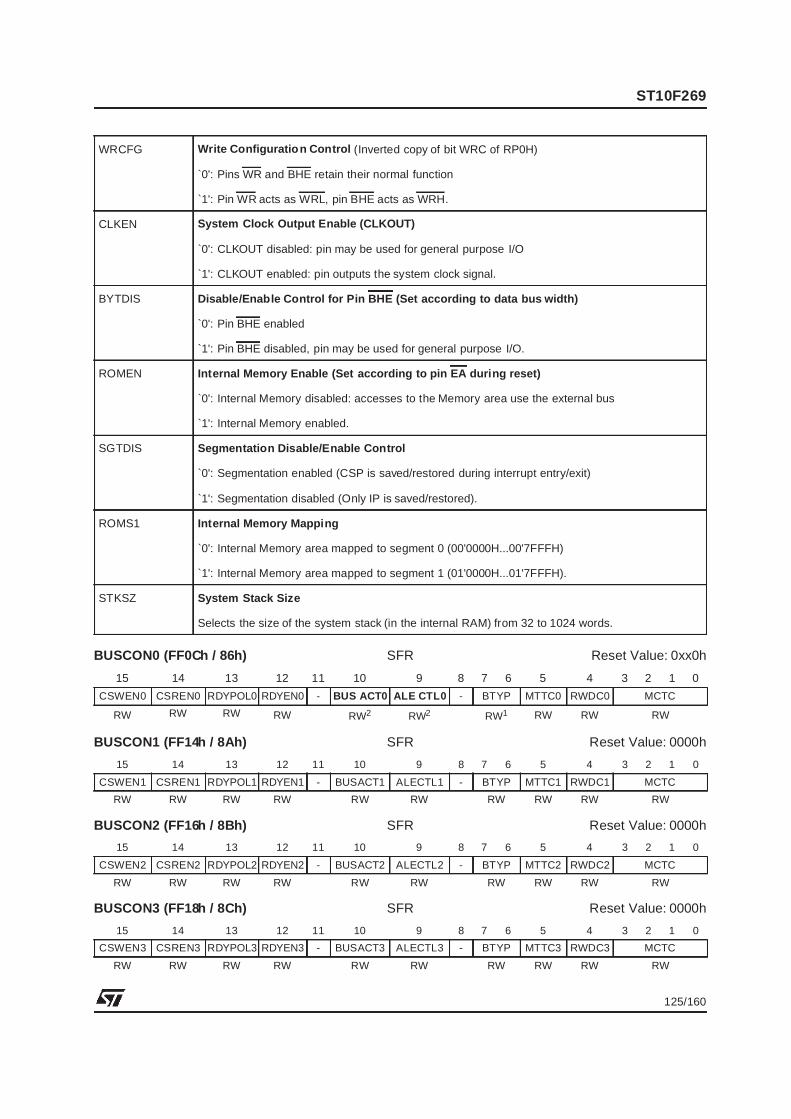
ST10F269
125/160
BUSCON0 (FF0Ch / 86h) SFR Reset Value: 0xx0h
BUSCON1 (FF14h / 8Ah) SFR Reset Value: 0000h
BUSCON2 (FF16h / 8Bh) SFR Reset Value: 0000h
BUSCON3 (FF18h / 8Ch) SFR Reset Value: 0000h
WRCFG Write Configuration Control (Inverted copy of bit WRC of RP0H)
`0': Pins WR and BHE retain their normal function
`1': Pin WR acts as WRL, pin BHE acts as WRH.
CLKEN System Clock Output Enable (CLKOUT)
`0': CLKOUT disabled: pin may be used for general purpose I/O
`1': CLKOUT enabled: pin outputs the system clock signal.
BYTDIS Disable/Enable Control for Pin BHE (Set according to data bus width)
`0': Pin BHE enabled
`1': Pin BHE disabled, pin may be used for general purpose I/O.
ROMEN Internal Memory Enable (Set according to pin EA during reset)
`0': Internal Memory disabled: accesses to the Memory area use the external bus
`1': Internal Memory enabled.
SGTDIS Segmentation Disable/Enable Control
`0': Segmentation enabled (CSP is saved/restored during interrupt entry/exit)
`1': Segmentation disabled (Only IP is saved/restored).
ROMS1 Internal Memory Mapping
`0': Internal Memory area mapped to segment 0 (00'0000H...00'7FFFH)
`1': Internal Memory area mapped to segment 1 (01'0000H...01'7FFFH).
STKSZ System Stack Size
Selects the size of the system stack (in the internal RAM) from 32 to 1024 words.
15 14 13 12 11 10 9 8 7 6 5 4 3 2 1 0
CSWEN0 CSREN0 RDYPOL0 RDYEN0 - BUS ACT0 ALE CTL0 - BTYP MTTC0 RWDC0 MCTC
RW RW RW RW RW2 RW2 RW1 RW RW RW
15 14 13 12 11 10 9 8 7 6 5 4 3 2 1 0
CSWEN1 CSREN1 RDYPOL1 RDYEN1 - BUSACT1 ALECTL1 - BTYP MTTC1 RWDC1 MCTC
RW RW RW RW RW RW RW RW RW RW
15 14 13 12 11 10 9 8 7 6 5 4 3 2 1 0
CSWEN2 CSREN2 RDYPOL2 RDYEN2 - BUSACT2 ALECTL2 - BTYP MTTC2 RWDC2 MCTC
RW RW RW RW RW RW RW RW RW RW
15 14 13 12 11 10 9 8 7 6 5 4 3 2 1 0
CSWEN3 CSREN3 RDYPOL3 RDYEN3 - BUSACT3 ALECTL3 - BTYP MTTC3 RWDC3 MCTC
RW RW RW RW RW RW RW RW RW RW

ST10F269
126/160
BUSCON4 (FF1Ah / 8Dh) SFR Reset Value: 0000h
Notes: 1. BTYP (bit 6 and 7) are set according to the configuration of the bit l6 and l7 of PORT0 latched at the end of the reset seque nce.2. BUSCON0 is initialized with 0000h, if EA pin is high during reset. If EA pin is low during reset, bit BUSACT0 and ALECTRL0 areset ('1') and bit field BTYP is loaded with the bus configuration selected via PORT0.
15 14 13 12 11 10 9 8 7 6 5 4 3 2 1 0
CSWEN4 CSREN4 RDYPOL4 RDYEN4 - BUSACT4 ALECTL4 - BTYP MTTC4 RWDC4 MCTC
RW RW RW RW RW RW RW RW RW RW
MCTC Memory Cycle Time Control (Number of memory cycle time wait states)
0 0 0 0: 15 wait states (Nber = 15 - [MCTC])
. . .
1 1 1 1: No wait state
RWDCx Read/Write Delay Control for BUSCONx
`0': With read/write delay: activate command 1 TCL after falling edge of ALE
`1': No read/write delay: activate command with falling edge of ALE
MTTCx Memory Tristate Time Control
`0': 1 wait state
`1': No wait state
BTYP External Bus Configuration
0 0: 8-bit Demultiplexed Bus
0 1: 8-bit Multiplexed Bus
1 0: 16-bit Demultiplexed Bus
1 1: 16-bit Multiplexed Bus
Note: For BUSCON0, BTYP bit-field is defined via PORT0 during reset.
ALECTLx ALE Lengthening Control
`0': Normal ALE signal
`1': Lengthened ALE signal
BUSACTx Bus Active Control
`0': External bus disabled
`1': External bus enabled (within the respective address window, seeADDRSEL)
RDYENx READY Input Enable
`0': External bus cycle is controlled by bit field MCTC only
`1': External bus cycle is controlled by the READY input signal
RDYPOLx Ready Active Level Control
`0': Active level on the READY pin is low, bus cycle terminates with a `0' onREADY pin,
`1': Active level on the READY pin is high, bus cycle terminates with a `1' onREADY pin.
CSRENx Read Chip Select Enable
`0': The CS signal is independent of the read command (RD)
`1': The CS signal is generated for the duration of the read command
CSWENx Write Chip Select Enable
`0': The CS signal is independent of the write command (WR,WRL,WRH)
`1': The CS signal is generated for the duration of the write command

ST10F269
127/160
RP0H (F108h / 84h) ESFR Reset Value: --XXH
Notes: 1. RP0H.7 to RP0H.5 bits are loaded only during a long hardware reset. As pull-up resistors are active on each Port P0H pinsduring reset, RP0H default value is ºFFhº.
2. These bits are set according to Port 0 configuration during any reset sequence.
3. RP0H is a read only register.
15 14 13 12 11 10 9 8 7 6 5 4 3 2 1 0
- - - - - - - - CLKSEL SALSEL CSSEL WRC
R 1 - 2 R 2 R 2 R 2
WRC 2 Write Configuration Control
`0': Pin WR acts as WRL, pin BHE acts as WRH
`1': Pins WR and BHE retain their normal function
CSSEL 2 Chip Select Line Selection (Number of active CS outputs)
0 0: 3 CS lines: CS2...CS0
0 1: 2 CS lines: CS1...CS0
1 0: No CS line at all
1 1: 5 CS lines: CS4...CS0 (Default without pull-downs)
SALSEL 2 Segment Address Line Selection (Number of active segment address outputs)
0 0: 4-bit segment address: A19...A16
0 1: No segment address lines at all
1 0: 8-bit segment address: A23...A16
1 1: 2-bit segment address: A17...A16 (Default without pull-downs)
CLKSEL 1 - 2 System Clock Selection
000: fCPU = 2.5 x fOSC
001: fCPU = 0.5 x fOSC
010: fCPU = 1.5 x fOSC
011: fCPU = fOSC
100: fCPU = 5 x fOSC
101: fCPU = 2 x fOSC
110: fCPU = 3 x fOSC
111: fCPU = 4 x fOSC

ST10F269
128/160
EXICON (F1C0h / E0h ESFR Reset Value: 0000h
EXISEL (F1DAh / EDh) ESFR Reset Value:0000h
XP3IC (F19Eh / CFh) 1 ESFR Reset Value: --00h
Note: 1. XP3IC register has the same bit field as xxIC interrupt registers
15 14 13 12 11 10 9 8 7 6 5 4 3 2 1 0
EXI7ES EXI6ES EXI5ES EXI4ES EXI3ES EXI2ES EXI1ES EXI0ES
RW RW RW RW RW RW RW RW
EXIxES(x=7...0) External Interrupt x Edge Selection Field (x=7...0)
0 0: Fast external interrupts disabled: standard mode
EXxIN pin not taken in account for entering/exiting Power Down mode.
0 1: Interrupt on positive edge (rising)
Enter Power Down mode if EXiIN = `0', exit if EXxIN = `1' (referred as `high' active level)
1 0: Interrupt on negative edge (falling)
Enter Power Down mode if EXiIN = `1', exit if EXxIN = `0' (referred as `low' active level)
1 1: Interrupt on any edge (rising or falling)
Always enter Power Down mode, exit if EXxIN level changed.
15 14 13 12 11 10 9 8 7 6 5 4 3 2 1 0
EXI7SS EXI6SS EXI5SS EXI4SS EXI3SS EXI2SS EXI1SS EXI0SS
RW RW RW RW RW RW RW RW
EXIxSS External Interrupt x Source Selection (x=7...0)
`00': Input from associated Port 2 pin.
`01': Input from ªalternate sourceº.
`10': Input from Port 2 pin ORed with ªalternate sourceº.
`11': Input from Port 2 pin ANDed with ªalternate sourceº.
EXIxSS Port 2 pin Alternate Source
0 P2.8 CAN1_RxD
1 P2.9 CAN2_RxD
2 P2.10 RTCSI
3 P2.11 RTCAI
4...7 P2.12...15 Not used (zero)
15 14 13 12 11 10 9 8 7 6 5 4 3 2 1 0
- - - - - - - - XP3IR XP3IE XP3ILVL GLVL
RW RW RW RW

ST10F269
129/160
xxIC (yyyyh / zzh) SFR Area ResetValue: --00h
XPERCON (F024h / 12h) ESFR Reset Value: --05h
15 14 13 12 11 10 9 8 7 6 5 4 3 2 1 0
- - - - - - - - xxIR xxIE ILVL GLVL
RW RW RW RW
Bit Function
GLVL Group Level
Defines the internal order for simultaneous requests of the same priority.3: Highest group priority0: Lowest group priority
ILVL Interrupt Priority Level
Defines the priority level for the arbitration of requests.Fh: Highest priority level0h: Lowest priority level
xxIE Interrupt Enable Control Bit (individually enables/disables a specific source)
`0': Interrupt Request is disabled`1': Interrupt Request is enabled
xxIR Interrupt Request Flag
`0': No request pending`1': This source has raised an interrupt request
15 14 13 12 11 10 9 8 7 6 5 4 3 2 1 0
- - - - - - - - - - - RTCEN XRAM2EN XRAM1EN CAN2EN CAN1EN
RW RW RW RW RW
CAN1EN CAN1 Enable Bit
`0': Accesses to the on-chip CAN1 XPeripheral and its functions are disabled. P4.5 and P4.6 pins can beused as general purpose I/Os. Address range 00'EF00h-00'EFFFh is only directed to external memory ifCAN2EN is also `0'.
`1': The on-chip CAN1 XPeripheral is enabled and can be accessed.
CAN2EN CAN2 Enable Bit
`0': Accesses to the on-chip CAN2 XPeripheral and its functions are disabled. P4.4 and P4.7 pins can beused as general purpose I/Os. Address range 00'EE00h-00'EEFFh is only directed to external memory ifCAN1EN is also `0'.
`1': The on-chip CAN2 XPeripheral is enabled and can be accessed.
XRAM1EN XRAM1 Enable Bit
`0': Accesses to external memory within space 00'E000h to 00'E7FFh. The 2K Bytes of internal XRAM1are disabled.
'1': Accesses to the internal 2K Bytes of XRAM1.
XRAM2EN XRAM2 Enable Bit
`0': Accesses to the external memory within space 00'C000h to 00'DFFFh. The 8K Bytes of internalXRAM2 are disabled.
'1': Accesses to the internal 8K Bytes of XRAM2.
RTCEN RTC Enable Bit
'0': Accesses to the on-chip Real Time Clock are disabled, external access performed. Address range00'EC00h-00'ECFFh is only directed to external memory if CAN1EN and CAN2EN are '0' also
'1': The on-chip Real Time Clock is enabled and can be accessed.
ST10F269
130/160
When both CAN are disabled via XPERCONsetting, then any access in the address range00'EE00h - 00'EFFFh will be directed to externalmemory interface, using the BUSCONx registercorresponding to address matching ADDRSELxregister. P4.4 and P4.7 can be used as GeneralPurpose I/O when CAN2 is not enabled, and P4.5and P4.6 can be used as General Purpose I/Owhen CAN1 is not enabled.The default XPER selection after Reset isidentical to XBUS configuration of ST10C167:XCAN1 is enabled, XCAN2 is disabled, XRAM1(2K Byte compatible XRAM) is enabled, XRAM2(new 8K Byte XRAM) is disabled.
Register XPERCON cannot be changed after theglobal enabling of XPeripherals, i.e. after setting ofbit XPEN in SYSCON register.
In EMUlation mode, all the XPERipherals areenabled (XPERCON bit are all set).
When the Real Time Clock is disabled (RTCEN =0), the clock oscillator is switch off if ST10 entersin power-down mode. Otherwise, when the RealTime Clock is enabled, the bit RTCOFF of theRTCCON register allows to choose thepower-down mode of the clock oscillator.

ST10F269
131/160
21 - ELECTRICAL CHARACTERISTICS
21.1 - Absolute Maximum Ratings
Note: 1. Stresses above those listed under ªAbsolute Maximum Ratingsº may cause permanent damage to the device. This is a stressrating only and functional operation of the device at these or any other conditions above those indicated in the operational sectionsof this specification is not implied. Exposure to absolute maximum rating conditions for extended periods may affect device reliability.During overload conditions (VIN > VDD or VIN < VSS) the voltage on pins with respect to ground (VSS) must not exceed the valuesdefined by the Absolute Maximum Ratings.
21.2 - Parameter Interpretation
The parameters listed in the following tables represent the characteristics of theST10F269 and itsdemands on the system. Where the ST10F269 logic provides signals with their respective timingcharacteristics, the symbol ªCCº for Controller Characteristics, is included in the ªSymbolº column.
Where the external system must provide signals with their respective timing characteristics to theST10F269, the symbol ªSRº for System Requirement, is included in the ªSymbolº column.
21.3 - DC Characteristics
VDD = 5V + 10%, VSS = 0V, fCPU = 40MHz, Reset active,TA = -40 to + 1255C
Symbol Parameter Value Unit
VDD Voltage on VDD pins with respect to ground1 -0.5, +6.5 V
VIO Voltage on any pin with respect to ground1 -0.5, (VDD +0.5) V
VAREF Voltage on VAREF pin with respect to ground1 -0.3, (VDD +0.3) V
IOV Input Current on any pin during overload condition1 -10, +10 mA
ITOV Absolute Sum of all input currents during overload condition1 |100| mA
Ptot Power Dissipation1 1.5 W
TA Ambient Temperature under bias -40, +125 5C
Tstg Storage Temperature1 -65, +150 5C
Symbol Parameter TestConditions Min. Max. Unit
VIL SR Input low voltage ± -0.5 0.2 VDD -0.1 V
VILS SR Input low voltage (special threshold) ± -0.5 2.0 V
VIH SRInput high voltage(all except RSTIN and XTAL1)
±0.2 VDD +
0.9VDD + 0.5 V
VIH1 SR Input high voltage RSTIN ± 0.6 VDD VDD + 0.5 V
VIH2 SR Input high voltage XTAL1 ± 0.7 VDD VDD + 0.5 V
VIHS SR Input high voltage (special threshold) ±0.8 VDD
-0.2VDD + 0.5 V
HYS Input Hysteresis (special threshold) 3 ± 250 ± mV
VOL CC Output low voltage (PORT0, PORT1, Port 4,ALE, RD, WR, BHE, CLKOUT, RSTOUT)
1 IOL = 2.4mA ± 0.45 V
VOL1 CC Output low voltage (all other outputs) 1 IOL1 = 1.6mA ± 0.45 V

ST10F269
132/160
Notes: 1. ST10F269 pins are equipped with low-noise output drivers which significantly improve the device's EMI performance. Theselow-noise drivers deliver their maximum current only until the respective target output level is reached. After this, the output currentis reduced. This results in increased impedance of the driver, which attenuates electrical noise from the connected PCB tracks. The
VOH CCOutput high voltage (PORT0, PORT1, Port4,ALE, RD, WR, BHE, CLKOUT, RSTOUT)
1 IOH = -500 m AIOH = -2.4mA
0.9 VDD2.4
±±
V
VOH1 CC Output high voltage (all other outputs)1/2 IOH = ± 250 m A
IOH = ± 1.6mA0.9 VDD
2.4±±
VV
η IOZ1 η CC Input leakage current (Port 5) 0V < VIN < VDD ± 200 nA
η IOZ2 η CC Input leakage current (all other) 0V < VIN < VDD ± 1 m A
η IOV η SR Overload current 3/4 ± 5 mA
RRST CC RSTIN pull-up resistor 3 ± 50 250 k W
IRWH Read / Write inactive current 5/6 VOUT = 2.4V ± -40 m A
IRWL Read / Write active current 5/7 VOUT = VOLmax -500 ± m A
IALEL ALE inactive current 5/6 VOUT = VOLmax 40 ± m A
IALEH ALE active current 5/7 VOUT = 2.4V ± 500 m A
IP6H Port 6 inactive current 5/6 VOUT = 2.4V ± -40 m A
IP6L Port 6 active current 5/7 VOUT = VOL1max -500 ± m A
IP0HPORT0 configuration current
5/6 VIN = VIHmin ± -10 m A
IP0L5/7 VIN = VILmax -100 ± m A
η IIL η CC XTAL1 input current 0V < VIN < VDD ± 20 m A
gm On-chip oscillator transconductance 3 5 - mA/V
CIO CC Pin capacitance (digital inputs / outputs) 3/5f = 1MHz,TA = 255C ± 10 pF
ICC Power supply current8 RSTIN = VIH1
fCPU in [MHz]± 20 + 2.5 x fCPU mA
IID Idle mode supply current9 RSTIN = VIH1
fCPU in [MHz]± 20 + fCPU mA
IPD Power-down mode supply current
10 VDD = 5.5VTA = 255C
TA = 1255C
±
_
15 11
190 11
m A
m A
IPD2Power-down mode supply current (Real timeclock enabled, oscillator enabled)
10
12
VDD = 5.5VTA = 555C
fOSC = 25MHz± 2 + fOSC / 4 mA
Symbol Parameter TestConditions Min. Max. Unit

ST10F269
133/160
current specified in column ªTest Conditionsº is delivered in any cases.
2. This specification is not valid for outputs which are switched to open drain mode. In this case the respective output will float and thevoltage results from the external circuitry.3. Partially tested, guaranteed by design characterization.
4. Overload conditions occur if the standard operating conditions are exceeded, i.e. the voltage on any pin exceeds the specifiedrange (i.e. VOV > VDD+0.5V or VOV < -0.5V). The absolute sum of input overload currents on all port pins may not exceed 50mA. The
supply voltage must remain within the specified limits.
5. This specification is only valid during Reset, or during Hold-mode or Adapt-mode. Port 6 pins are only affected if they are used forCS output and if their open drain function is not enabled.
6. The maximum current may be drawn while the respective signal line remains inactive.
7. The minimum current must be drawn in order to drive the respective signal line active.
8. The power supply current is a function of the operating frequency. This dependency is illustrated in the Figure 64. Theseparameters are tested at VDDmax and 40MHz CPU clock with all outputs disconnected and all inputs at VIL or VIH. The chip is
configured with a demultiplexed 16-bit bus, direct clock drive, 5 chip select lines and 2 segment address lines, EA pin is low duringreset. After reset, PORT 0 is driven with the value `00CCh' that produces infinite execution of NOP instruction with 15 wait-states, R/W delay, memory tristate wait state, normal ALE. Peripherals are not activated.
9. Idle mode supply current is a function of the operating frequency. This dependency is illustrated in the Figure 64. Theseparameters are tested at VDDmax and 40MHz CPU clock with all outputs disconnected and all inputs at VIL or VIH.
10. This parameter value includes leakage currents. With all inputs (including pins configured as inputs) at 0V to 0.1V or atVDD ± 0.1V to VDD, VREF = 0V, all outputs (including pins configured as outputs) disconnected.
11. Typical IPD value is 5 m A @ TA=255C. and 60 m A @ TA=1255C.
12. Partially tested, guaranted by design characterization using 22pF loading capacitors on crystal pins.
Figure 64 : Supply / Idle Current as a Function of Operating Frequency
I [mA]
fCPU [MHz]10 20
100
10
ICCtyp
IIDmax
ICCmax
IIDtyp
4030
60mA
120mA
0

ST10F269
134/160
21.3.1 - A/D Converter Characteristics
VDD = 5V + 10%, VSS = 0V, TA = -40 to +1255C, 4.0V3 VAREF 3 VDD + 0.1V;VSS0.1V 3 VAGND 3 VSS + 0.2V
Notes: 1. VAIN may exceed VAGND or VAREF up to the absolute maximum ratings. However, the conversion result in these cases will beX000h or X3FFh, respectively.
2. During the tS sample time the input capacitance Cain can be charged/discharged by the external source. The internal resistance ofthe analog source must allow the capacitance to reach its final voltage level within the tS sample time. After the end of the tS sampletime, changes of the analog input voltage have no effect on the conversion result. Values for the tSC sample clock depend on theprogramming. Referring to the tC conversion time formula of Section 21.3.2 - on page 135 and to Table 33 on page 135:
- tS min = 2 tSC min = 2 tCC min = 2 x 24 x TCL = 48 TCL
- tS max = 2 tSC max = 2 x 8 tCC max = 2 x 8 x 96 TCL = 1536 TCLTCL is defined in Section 21.4.2 -, Section 21.4.4 -, and Section 21.4.5 - on page 138 :
3. The conversion time formula is:- tC = 14 tCC + tS + 4 TCL (= 14 tCC + 2 tSC + 4 TCL)
The tC parameter includes the tS sample time, the time for determining the digital result and the time to load the result register withthe result of the conversion. Values for the tCC conversion clock depend on the programming. Referring to Table 33 on page 135:
- tC min = 14 tCC min + tS min + 4 TCL = 14 x 24 x TCL + 48 TCL + 4 TCL = 388 TCL- tC max = 14 tCC max + tS max + 4 TCL = 14 x 96 TCL + 1536 TCL + 4 TCL = 2884 TCL
4. This parameter is fixed by ADC control logic.
5. DNL, INL, TUE are tested at VAREF = 5.0V, VAGND = 0V, VCC = 4.9V. It is guaranteed by design characterization for all othervoltages within the defined voltage range.`LSB' has a value of VAREF / 1024.The specified TUE is guaranteed only if an overload condition (see IOV specification) occurs on maximum 2 not selected analog inputpins and the absolute sum of input overload currents on all analog input pins does not exceed 10mA.
6. The coupling factor is measured on a channel while an overload condition occurs on the adjacent not selected channel with anabsolute overload current less than 10mA.
7. Partially tested, guaranteed by design characterization.
8.To remove noise and undesirable high frequency components from the analog input signal, a low-pass filter must be connected atthe ADC input. The cut-off frequency of this filter should avoid 2 opposite transitions during the ts sampling time of the ST10 ADC:
- fcut-off 3 1 / 5 ts to 1/10 tswhere ts is the sampling time of the ST10 ADC and is not related to the Nyquist frequency determined by the tc conversion time.
Table 32 : A/D Converter Characteristics
Symbol Parameter Test ConditionLimit Values
Unitminimum maximum
VAREF SR Analog Reference voltage 4.0 VDD + 0.1 V
VAIN SR Analog input voltage 1 - 8 VAGND VAREF V
IAREF CC Reference supply currentrunning modepower-down mode
7
±±
5001
m Am A
CAIN CC ADC input capacitanceNot samplingSampling
7
±±
1015
pFpF
tS CC Sample time 2 - 4 48 TCL 1 536 TCL
tC CC Conversion time 3 - 4 388 TCL 2 884 TCL
DNL CC Differential Nonlinearity 5 -0.5 +0.5 LSB
INL CC Integral Nonlinearity 5 -1.5 +1.5 LSB
OFS CC Offset Error 5 -1.0 +1.0 LSB
TUE CC Total unadjusted error 5 -2.0 +2.0 LSB
RASRC SR Internal resistance of analog source tS in [ns] 2 - 7 ± (tS / 150) - 0.25 k W
K CC Coupling Factor between inputs 6 - 7 ± 1/500

ST10F269
135/160
21.3.2 - Conversion Timing Control
When a conversion is started, first thecapacitances of the converter are loaded via therespective analog input pin to the current analoginput voltage. The time to load the capacitances isreferred to as the sample time ts. Next thesampled voltage is converted to a digital value in10 successive steps, which correspond to the10-bit resolution of the ADC. The next 4 steps areused for equalizing internal levels (and are keptfor exact timing matching with the 10-bit A/Dconverter module implemented in the ST10F168).
The current that has to be drawn from the sourcesfor sampling and changing charges depends onthe time that each respective step takes, becausethe capacitors must reach their final voltage levelwithin the given time, at least with a certainapproximation. The maximum current, however,that a source can deliver, depends on its internalresistance.
The sample time tS (= 2 tSC) and the conversiontime tc (= 14 tCC + 2 tSC + 4 TCL) can beprogrammed relatively to the ST10F269 CPU
clock. This allows adjusting the A/D converter ofthe ST10F269 to the properties of the system:Fast Conversion can be achieved byprogramming the respective times to theirabsolute possible minimum. This is preferable forscanning high frequency signals. The internalresistance of analog source and analog supplymust be sufficiently low, however.High Internal Resistance can be achieved byprogramming the respective times to a highervalue, or the possible maximum. This is preferablewhen using analog sources and supply with a highinternal resistance in order to keep the current aslow as possible. However the conversion rate inthis case may be considerably lower.The conversion times are programmed via theupper four bit of register ADCON. Bit field ADCTC(conversion time control) selects the basicconversion clock tCC, used for the 14 steps ofconverting. The sample time tS is a multiple of thisconversion time and is selected by bit fieldADSTC (sample time control). The table belowlists the possible combinations. The timings referto the unit TCL, where fCPU = 1/2TCL.
A complete conversion will take 14tCC + 2 tSC + 4 TCL (fastest convertion rate = 4.85m s at 40MHz). Thistime includes the conversion itself, the sample time and the time required to transfer the digital value tothe result register.
Table 33 : ADC Sampling and Conversion Timing
ADCTC
Conversion Clock t CC
ADSTC
Sample Clock t SC
TCL = 1/2 x fXTAL At f CPU = 40MHz tSC = At f CPU = 40MHzand ADCTC = 00
00 TCL x 24 0.3 m s 00 tCC 0.3 m s
01 Reserved, do not use Reserved 01 tCC x 2 0.6 m s
10 TCL x 96 1.2 m s 10 tCC x 4 1.2 m s
11 TCL x 48 0.6 m s 11 tCC x 8 2.4 m s

ST10F269
136/160
21.4 - AC characteristics
21.4.1 - Test Waveforms
21.4.2 - Definition of Internal Timing
The internal operation of the ST10F269 iscontrolled by the internal CPU clock fCPU. Bothedges of the CPU clock can trigger internal (forexample pipeline) or external (for example buscycles) operations.
The specification of the external timing (ACCharacteristics) therefore depends on the timebetween two consecutive edges of the CPU clock,called ªTCLº.
The CPU clock signal can be generated bydifferent mechanisms. The duration of TCL and itsvariation (and also the derived external timing)depends on the mechanism used to generatefCPU.
This influence must be regarded when calculatingthe timings for the ST10F269.
The example for PLL operation shown in Figure67 refers to a PLL factor of 4.
Figure 65 : Input / Output Waveforms
Figure 66 : Float Waveforms
2.4V
0.45V
Test Points
0.2VDD+0.9 0.2VDD+0.9
0.2VDD-0.1 0.2VDD-0.1
AC inputs during testing are driven at 2.4V for a logic `1' and 0.4V for a logic `0'.Timing measurements are made at VIH min for a logic `1' and VIL max for a logic `0'.
TimingReference
Points
VLoad +0.1V
VLoad -0.1V
VOH -0.1V
VOL +0.1V
VLoad
VOL
VOH
For timing purposes a port pin is no longer floating when VLOAD changes of +100mV.It begins to float when a 100mV change from the loaded VOH/VOL level occurs (IOH/IOL = 20mA).

ST10F269
137/160
The mechanism used to generate the CPU clock is selected during reset by the logic levels on pinsP0.15-13 (P0H.7-5).
21.4.3 - Clock Generation ModesThe Table 34 associates the combinations of these three bits with the respective clock generation mode.
Notes: 1. The external clock input range refers to a CPU clock range of 1...40MHz.2. The maximum input frequency depends on the duty cycle of the external clock signal.3. The maximum input frequency is 25MHz when using an external crystal with the internal oscillator; providing that internal serialresistance of the crystal is less than 40 W . However, higher frequencies can be applied with an external clock source on pin XTAL1,but in this case, the input clock signal must reach the defined levels VIL and VIH2..
Figure 67 : Generation Mechanisms for the CPU Clock
Table 34 : CPU Frequency Generation
P0H.7 P0H.6 P0H.5 CPU Frequency f CPU = fXTAL x F External Clock Input Range 1 Notes
1 1 1 fXTAL x 4 2.5 to 10MHz Default configuration
1 1 0 fXTAL x 3 3.33 to 13.33MHz
1 0 1 fXTAL x 2 5 to 20MHz
1 0 0 fXTAL x 5 2 to 8MHz
0 1 1 fXTAL x 1 1 to 40MHz Direct drive2
0 1 0 fXTAL x 1.5 6.66 to 26.66MHz
0 0 1 fXTAL x 0.5 2 to 80MHz CPU clock via prescaler3
0 0 0 fXTAL x 2.5 4 to 16MHz
TCL TCL
TCL TCL
fCPU
fXTAL
fCPU
fXTAL
Phase locked loop operation
Direct Clock Drive
TCL TCL
fCPU
fXTAL
Prescaler Operation

ST10F269
138/160
21.4.4 - Prescaler Operation
When pins P0.15-13 (P0H.7-5) equal '001' duringreset, the CPU clock is derived from the internaloscillator (input clock signal) by a 2:1 prescaler.The frequency of fCPU is half the frequency offXTAL and the high and low time of fCPU (i.e. theduration of an individual TCL) is defined by theperiod of the input clock fXTAL.
The timings listed in the AC Characteristics thatrefer to TCL therefore can be calculated using theperiod of fXTAL for any TCL.
Note that if the bit OWDDIS in SYSCON registeris cleared, the PLL runs on its free-runningfrequency and delivers the clock signal for theOscillator Watchdog. If bit OWDDIS is set, thenthe PLL is switched off.
21.4.5 - Direct Drive
When pins P0.15-13 (P0H.7-5) equal '011' duringreset the on-chip phase locked loop is disabledand the CPU clock is directly driven from theinternal oscillator with the input clock signal.
The frequency of fCPU directly follows thefrequency of fXTAL so the high and low time of fCPU(i.e. the duration of an individual TCL) is definedby the duty cycle of the input clock fXTAL.
Therefore, the timings given in this chapter refer tothe minimum TCL. This minimum value can becalculated by the following formula:
For two consecutive TCLs, the deviation causedby the duty cycle of fXTAL is compensated, so theduration of 2TCL is always 1/fXTAL.
The minimum value TCLmin has to be used onlyonce for timings that require an odd number ofTCLs (1,3,...). Timings that require an evennumber of TCLs (2,4,...) may use the formula:
Note: The address float timings in Multiplexedbus mode (t11 and t45) use the maximumduration of TCL (TCLmax = 1/fXTAL xDCmax) instead of TCLmin.If the bit OWDDIS in SYSCON register iscleared, the PLL runs on its free-runningfrequency and delivers the clock signal forthe Oscillator Watchdog. If bit OWDDIS isset, then the PLL is switched off.
21.4.6 - Oscillator Watchdog (OWD)
An on-chip watchdog oscillator is implemented inthe ST10F269. This feature is used for safetyoperation with external crystal oscillator (usingdirect drive mode with or without prescaler). Thiswatchdog oscillator operates as following :
The reset default configuration enables thewatchdog oscillator. It can be disabled by settingthe OWDDIS (bit 4) of SYSCON register.
When the OWD is enabled, the PLL runs at itsfree-running frequency, and it increments thewatchdog counter. The PLL free-runningfrequency is between 2 and 10MHz. On eachtransition of external clock, the watchdog counteris cleared. If an external clock failure occurs, thenthe watchdog counter overflows (after 16 PLLclock cycles).
The CPU clock signal will be switched to the PLLfree-running clock signal, and the oscillatorwatchdog Interrupt Request (XP3INT) is flagged.The CPU clock will not switch back to the externalclock even if a valid external clock exits on XTAL1pin. Only a hardware reset can switch the CPUclock source back to direct clock input.
When the OWD is disabled, the CPU clock isalways external oscillator clock and the PLL isswitched off to decrease consumption supplycurrent.
21.4.7 - Phase Locked Loop
For all other combinations of pins P0.15-13(P0H.7-5) during reset the on-chip phase lockedloop is enabled and it provides the CPU clock (seeTable 34). The PLL multiplies the input frequencyby the factor F which is selected via thecombination of pins P0.15-13 (fCPU = fXTAL x F).With every F'th transition of fXTAL the PLL circuitsynchronizes the CPU clock to the input clock.This synchronization is done smoothly, so theCPU clock frequency does not change abruptly.
Due to this adaptation to the input clock thefrequency of fCPU is constantly adjusted so it islocked to fXTAL. The slight variation causes a jitterof fCPU which also effects the duration ofindividual TCLs.
The timings listed in the AC Characteristics thatrefer to TCLs therefore must be calculated usingthe minimum TCL that is possible under therespective circumstances.
TCLmin 1 f6 XTAL lx l DCmin=
DC duty cycle=
2TCL 1 fXTAL6=

ST10F269
139/160
The real minimum value for TCL depends on thejitter of the PLL. The PLL tunes fCPU to keep itlocked on fXTAL. The relative deviation of TCL isthe maximum when it is refered to one TCLperiod. It decreases according to the formula andto the Figure 68 given below. ForN periods of TCLthe minimum value is computed using thecorresponding deviation DN:
where N = number of consecutive TCL periodsand 1 3 N 3 40. So for a period of 3 TCL periods(N = 3):D3 = 4 - 3/15 = 3.8%3TCLmin = 3TCLNOM x (1 - 3.8/100)
= 3TCLNOM x 0.9623TCLmin = 36.075ns (at fCPU = 40MHz)This is especially important for bus cycles using waitstates and e.g. for the operation of timers, serialinterfaces, etc. For all slower operations and longerperiods (e.g. pulse train generation or measurement,lower Baud rates, etc.) the deviation caused by thePLL jitter is negligible.
21.4.8 - External Clock Drive XTAL1VDD = 5V + 10%, VSS = 0V, TA = -40 to +125 5C
Notes: 1. Theoretical minimum. The real minimum value depends on the duty cycle of the input clock signal. 25MHz is the maximum inputfrequency when using an external crystal oscillator. However, 40MHz can be applied with an external clock source.2. The input clock signal must reach the defined levels VIL and VIH2.
TCLMIN T CLNOM 1DN
100-------------±
Υ <Ψ ΜΨ ΜΤ Ν
ψ=
DN 4 N 15 ) %[ ]6±(+=
Figure 68 : Approximated Maximum PLL Jitter
Parameter SymbolfCPU = fXTAL fCPU = fXTAL / 2
fCPU = fXTAL x F
F = 1.5/2,/2.5/3/4/5 Unit
min max min max min max
Oscillator period tOSC SR 25 1 ± 12.5 ± 40 x N 100 x N ns
High time t1 SR 10 2 ± 5 2 ± 10 2 ± ns
Low time t2 SR 10 2 ± 5 2 ± 10 2 ± ns
Rise time t3 SR ± 3 2 ± 3 2 ± 3 2 ns
Fall time t4 SR ± 3 2 ± 3 2 ± 3 2 ns
3216842
+1
+2
+3
+4
Max.jitter [%]
N
This approximated formula is valid for1 3 N 3 40 and 10MHz 3 fCPU 3 40MHz.

ST10F269
140/160
Figure 69 : External Clock Drive XTAL1
21.4.9 - Memory Cycle VariablesThe tables below use three variables which are derived from the BUSCONx registers and represent thespecial characteristics of the programmed memory cycle. The following table describes, how thesevariables are to be computed.
Description Symbol Values
ALE Extension tA TCL x [ALECTL]
Memory Cycle Time wait states tC 2TCL x (15 - [MCTC])
Memory Tri-state Time tF 2TCL x (1 - [MTTC])
t1 t3 t4
VIL
t2
tOSC
VIH2

ST10F269
141/160
21.4.10 - Multiplexed Bus
VDD = 5V + 10%, VSS = 0V, TA = -40 to +1255C, CL = 50pF,ALE cycle time = 6 TCL + 2tA + tC + tF (75ns at 40MHz CPU clock without wait states).
Table 35 : Multiplexed Bus Characteristics
Symbol Parameter
Max. CPU Clock= 40MHz
Variable CPU Clock1/2 TCL = 1 to 40MHz
Uni
t
min. max. min. max.
t5 CC ALE high time 4 + tA ± TCL - 8.5 + tA ± ns
t6 CC Address setup to ALE 2 + tA ± TCL - 10.5 + tA ± ns
t7 CC Address hold after ALE 1 4 + tA ± TCL - 8.5 + tA ± ns
t8 CC ALE falling edge to RD, WR(with RW-delay)
4 + tA ± TCL - 8.5 + tA ± ns
t9 CC ALE falling edge to RD, WR (noRW-delay)
-8.5 + tA ± -8.5 + tA ± ns
t10 CC Address float after RD, WR(with RW-delay) 1
± 6 ± 6 ns
t11 CC Address float after RD, WR(no RW-delay) 1
± 18.5 ± TCL + 6 ns
t12 CC RD, WR low time(with RW-delay)
15.5 + tC ± 2 TCL -9.5 + tC ± ns
t13 CC RD, WR low time(no RW-delay)
28 + tC ± 3 TCL -9.5 + tC ± ns
t14 SR RD to valid data in(with RW-delay)
± 6 + tC ± 2 TCL - 19 + tC ns
t15 SR RD to valid data in(no RW-delay)
± 18.5 + tC ± 3 TCL - 19 + tC ns
t16 SR ALE low to valid data in ± 18.5+ tA + tC
± 3 TCL - 19+ tA + tC
ns
t17 SR Address/Unlatched CS to validdata in
± 22 + 2tA +tC
± 4 TCL - 28+ 2tA + tC
ns
t18 SR Data hold after RDrising edge
0 ± 0 ± ns
t19 SR Data float after RD 1 ± 16.5 + tF ± 2 TCL - 8.5 + tF ns
t22 CC Data valid to WR 10 + tC ± 2 TCL -15 + tC ± ns
t23 CC Data hold after WR 4 + tF ± 2 TCL - 8.5 + tF ± ns
t25 CC ALE rising edge after RD, WR 15 + tF ± 2 TCL -10 + tF ± ns
t27 CC Address/Unlatched CS holdafter RD, WR
10 + tF ± 2 TCL -15 + tF ± ns
t38 CC ALE falling edge to Latched CS -4 - tA 10 - tA -4 - tA 10 - tA ns
t39 SR Latched CS low to Valid Data In ± 18.5 + tC +2tA
± 3 TCL - 19+ tC + 2tA
ns
t40 CC Latched CS hold after RD, WR 27 + tF ± 3 TCL - 10.5 + tF ± ns

ST10F269
142/160
Note: 1. Partially tested, guaranted by design characterization.
t42 CC ALE fall. edge to RdCS, WrCS(with RW delay)
7 + tA ± TCL - 5.5+ tA ± ns
t43 CC ALE fall. edge to RdCS, WrCS(no RW delay)
-5.5 + tA ± -5.5 + tA ± ns
t44 CC Address float after RdCS,WrCS (with RW delay) 1
± 0 ± 0 ns
t45 CC Address float after RdCS,WrCS (no RW delay) 1
± 12.5 ± TCL ns
t46 SR RdCS to Valid Data In(with RW delay)
± 4 + tC ± 2 TCL - 21 + tC ns
t47 SR RdCS to Valid Data In(no RW delay)
± 16.5 + tC ± 3 TCL - 21 + tC ns
t48 CC RdCS, WrCS Low Time(with RW delay)
15.5 + tC ± 2 TCL - 9.5 + tC ± ns
t49 CC RdCS, WrCS Low Time(no RW delay)
28 + tC ± 3 TCL - 9.5 + tC ± ns
t50 CC Data valid to WrCS 10 + tC ± 2 TCL - 15+ tC ± ns
t51 SR Data hold after RdCS 0 ± 0 ± ns
t52 SR Data float after RdCS 1 ± 16.5 + tF ± 2 TCL - 8.5+tF ns
t54 CC Address hold afterRdCS, WrCS
6 + tF ± 2 TCL - 19 + tF ± ns
t56 CC Data hold after WrCS 6 + tF ± 2 TCL - 19 + tF ± ns
Table 35 : Multiplexed Bus Characteristics
Symbol Parameter
Max. CPU Clock= 40MHz
Variable CPU Clock1/2 TCL = 1 to 40MHz
Uni
t
min. max. min. max.

ST10F269
143/160
Figure 70 : External Memory Cycle : Multiplexed Bus, With / Without Read / Write Delay, Normal ALE
Data In
Data OutAddress
Address
t38
t10
Read Cycle
Write Cycle
t5 t16
t39
t40
t25
t27
t18
t14
t22
t23
t12
t8
t8
t6m
t19
Address
t17
t6
t7
t9t11
t13
t15
t16
t12t13
Address
t9
t17
t6
t27
CLKOUT
ALE
CSx
A23-A16(A15-A8)
Address/Data
RD
WRWRL
BHE
WRH
Bus (P0)
Address/DataBus (P0)

ST10F269
144/160
Figure 71 : External Memory Cycle: Multiplexed Mus, With / Without Read / Write Delay, Extended ALE
Data OutAddress
Data InAddress
Address
t5 t16
t6 t7
t39
t40
t14
t8
t18
t23
t6
t27
t38
t10 t19
t25
t17
t9 t11
t15
t12
t13
t8 t10
t9t11
t12t13
t22
t27
t17
t6
Read Cycle
Write Cycle
CLKOUT
ALE
CSx
A23-A16(A15-A8)
RD
WRWRL
BHE
WRH
Address/DataBus (P0)
Address/DataBus (P0)

ST10F269
145/160
Figure 72 : External Memory Cycle: Multiplexed Bus, With / Without Read / Write Delay, Normal ALE,Read / Write Chip Select
Read Cycle
Write Cycle
CLKOUT
ALE
A23-A16(A15-A8)BHE
Data In
Data OutAddress
Address
t44
t5 t16t25
t27
t51
t46
t50
t56
t48
t42
t42
t6
t52
Address
t17
t6
t7
t43t45
t49
t47
t16
t48t49
Address
t43
RdCSx
WrCSx
Address/DataBus (P0)
Address/DataBus (P0)

ST10F269
146/160
Figure 73 : External Memory Cycle: Multiplexed Bus, With / Without Read / Write Delay, Extended ALE,Read / Write Chip Select
Data OutAddress
Data InAddress
Address
t5 t16
t6 t7
t46
t42
t42
t50
t18
t56
t6
t54
t44
t19
t25
t17
t43 t45
t47
t48
t49
t49
t43
t48
t44
t45
Read Cycle
Write Cycle
CLKOUT
ALE
A23-A16(A15-A8)BHE
RdCSx
WrCSx
Address/DataBus (P0)
Address/DataBus (P0)

ST10F269
147/160
21.4.11 - Demultiplexed BusVDD = 5V + 10%, VSS = 0V, TA = -40 to +1255C, CL = 50pF,ALE cycle time = 4 TCL + 2tA + tC + tF (50ns at 40MHz CPU clock without wait states).
Table 36 : Demultiplexed Bus Characteristics
Symbol Parameter
Maximum CPU Clock= 40MHz
Variable CPU Clock1/2 TCL = 1 to 40MHz
Uni
t
Minimum Maximum Minimum Maximum
t5 CC ALE high time 4 + tA ± TCL - 8.5 + tA ± ns
t6 CC Address setup to ALE 2 + tA ± TCL - 10.5 + tA ± ns
t80 CC Address/Unlatched CS setup toRD, WR(with RW-delay)
16.5 + 2tA ± 2 TCL - 8.5 + 2tA ± ns
t81 CC Address/Unlatched CS setup toRD, WR(no RW-delay)
4 + 2tA ± TCL - 8.5 + 2tA ± ns
t12 CC RD, WR low time(with RW-delay)
15.5 + tC ± 2 TCL - 9.5 + tC ± ns
t13 CC RD, WR low time(no RW-delay)
28 + tC ± 3 TCL - 9.5 + tC ± ns
t14 SR RD to valid data in(with RW-delay)
± 6 + tC ± 2 TCL - 19 + tC ns
t15 SR RD to valid data in(no RW-delay)
± 18.5 + tC ± 3 TCL - 19 + tC ns
t16 SR ALE low to valid data in ± 18.5 + tA +tC
± 3 TCL - 19+ tA + tC
ns
t17 SR Address/Unlatched CS to validdata in
± 22 + 2tA +tC
± 4 TCL - 28+ 2tA + tC
ns
t18 SR Data hold after RDrising edge
0 ± 0 ± ns
t20 SR Data float after RD rising edge(with RW-delay) 1 3
± 16.5 + tF ± 2 TCL - 8.5+ tF + 2tA
1ns
t21 SR Data float after RD rising edge(no RW-delay) 1 3
± 4 + tF ± TCL - 8.5+ tF + 2tA
1ns
t22 CC Data valid to WR 10 + tC ± 2 TCL - 15 + tC ± ns
t24 CC Data hold after WR 4 + tF ± TCL - 8.5 + tF ± ns
t26 CC ALE rising edge after RD, WR -10 + tF ± -10 + tF ± ns
t28 CC Address/Unlatched CS holdafter RD, WR 2
0 (no tF)-5 + tF(tF > 0)
± 0 (no tF)-5 + tF(tF > 0)
± ns
t28h CC Address/Unlatched CS hold
after WRH
-5 + tF ± -5 + tF ± ns
t38 CC ALE falling edge to Latched CS -4 - tA 6 - tA -4 - tA 6 - tA ns
t39 SR Latched CS low to Valid Data In ± 18.5+ tC + 2tA
± 3 TCL - 19+ tC + 2tA
ns
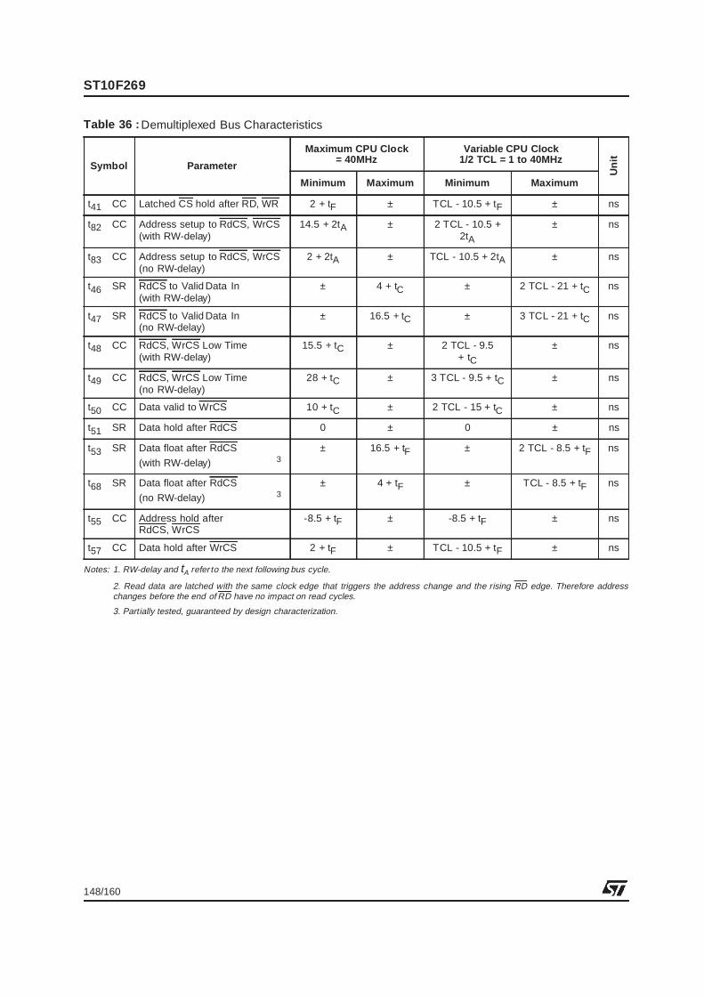
ST10F269
148/160
Notes: 1. RW-delay and tA refer to the next following bus cycle.
2. Read data are latched with the same clock edge that triggers the address change and the rising RD edge. Therefore addresschanges before the end of RD have no impact on read cycles.
3. Partially tested, guaranteed by design characterization.
t41 CC Latched CS hold after RD, WR 2 + tF ± TCL - 10.5 + tF ± ns
t82 CC Address setup to RdCS, WrCS(with RW-delay)
14.5 + 2tA ± 2 TCL - 10.5 +2tA
± ns
t83 CC Address setup to RdCS, WrCS(no RW-delay)
2 + 2tA ± TCL - 10.5 + 2tA ± ns
t46 SR RdCS to Valid Data In(with RW-delay)
± 4 + tC ± 2 TCL - 21 + tC ns
t47 SR RdCS to Valid Data In(no RW-delay)
± 16.5 + tC ± 3 TCL - 21 + tC ns
t48 CC RdCS, WrCS Low Time(with RW-delay)
15.5 + tC ± 2 TCL - 9.5+ tC
± ns
t49 CC RdCS, WrCS Low Time(no RW-delay)
28 + tC ± 3 TCL - 9.5 + tC ± ns
t50 CC Data valid to WrCS 10 + tC ± 2 TCL - 15 + tC ± ns
t51 SR Data hold after RdCS 0 ± 0 ± ns
t53 SR Data float after RdCS
(with RW-delay) 3± 16.5 + tF ± 2 TCL - 8.5 + tF ns
t68 SR Data float after RdCS
(no RW-delay) 3± 4 + tF ± TCL - 8.5 + tF ns
t55 CC Address hold afterRdCS, WrCS
-8.5 + tF ± -8.5 + tF ± ns
t57 CC Data hold after WrCS 2 + tF ± TCL - 10.5 + tF ± ns
Table 36 : Demultiplexed Bus Characteristics
Symbol Parameter
Maximum CPU Clock= 40MHz
Variable CPU Clock1/2 TCL = 1 to 40MHz
Uni
t
Minimum Maximum Minimum Maximum

ST10F269
149/160
Figure 74 : External Memory Cycle: Demultiplexed Bus, With / Without Read / Write Delay, Normal ALE
Note: 1. Un-latched CSx = t41u = t41 TCL =10.5 + tF.
Write Cycle
CLKOUT
ALE
A23-A16A15-A0 (P1)BHE
WRWRLWRH
Data In
Data Out
t38
t5 t16
t39
t41
t18
t14
t22
t12
Address
t17
t13
t15
t12
t13
t21
t20
t81
t80
t26
t24
t17
t6
t41u
t6
t80
t81
t28 (or t28h)
CSx
Read CycleData Bus (P0)
RD
1)
(D15-D8) D7-D0
Data Bus (P0)(D15-D8) D7-D0

ST10F269
150/160
Figure 75 : External Memory Cycle: Demultiplexed Bus, With / Without Read / Write Delay, Extended ALE
Address
t5t16
t39
t41
t14
t24
t6
t38
t20
t26
t17
t15
t12
t13
t12
t13
t22
Data In
t18
t21
t6
t17 t28
t28
Data Out
t80
t81
t80
t81
Read Cycle
Write Cycle
CLKOUT
ALE
CSx
RD
WRWRLWRH
Data Bus (P0)(D15-D8) D7-D0
Data Bus (P0)(D15-D8) D7-D0
A23-A16A15-A0 (P1)BHE

ST10F269
151/160
Figure 76 : External Memory Cycle: Demultiplexed Bus, With / Without Read / Write Delay, Normal ALE,Read / Write Chip Select
Read Cycle
Write Cycle
CLKOUT
ALE
Data In
Data Out
t5 t16
t51
t46
t50
t48
Address
t17
t49
t47
t48
t49
t68
t53
t83
t82
t26
t57
t55
t6
t82
t83
RdCSx
WrCSx
Data Bus (P0)(D15-D8) D7-D0
Data Bus (P0)(D15-D8) D7-D0
A23-A16A15-A0 (P1)BHE

ST10F269
152/160
Figure 77 : External Memory Cycle: Demultiplexed Bus, no Read / Write Delay, Extended ALE, Read /Write Chip Select
Address
t5t16
t46
t57
t6
t53
t26
t17
t47
t48
t49
t48
t49
t50
Data In
t51
t68
t55
Data Out
t82
t83
t82
t83
Read Cycle
Write Cycle
CLKOUT
ALE
RdCSx
WrCSx
Data Bus (P0)(D15-D8) D7-D0
Data Bus (P0)(D15-D8) D7-D0
A23-A16A15-A0 (P1)
BHE

ST10F269
153/160
21.4.12 - CLKOUT andREADYVDD = 5V + 10%, VSS = 0V, TA = -40 to + 1255C, CL = 50pF
Notes: 1. These timings are given for test purposes only, in order to assure recognition at a specific clock edge.
2. Demultiplexed bus is the worst case. For multiplexed bus 2TCL are to be added to the maximum values. This adds even more timefor deactivating READY.The 2tA and tC refer to the next following bus cycle, tF refers to the current bus cycle.
Table 37 : CLKOUT and READY Characteristics
Symbol Parameter
Maximum CPU Clock= 40 MHz
Variable CPU Clock1/2TCL = 1 to 40 MHz
Uni
t
Minimum Maximum Minimum Maximum
t29 CC CLKOUT cycle time 25 25 2TCL 2TCL ns
t30 CC CLKOUT high time 4 ± TCL ± 8.5 ± ns
t31 CC CLKOUT low time 3 ± TCL ± 9.5 ± ns
t32 CC CLKOUT rise time ± 4 ± 4 ns
t33 CC CLKOUT fall time ± 4 ± 4 ns
t34 CC CLKOUT rising edge toALE falling edge
-2 + tA 8 + tA -2 + tA 8 + tA ns
t35 SR Synchronous READYsetup time to CLKOUT
12.5 ± 12.5 ± ns
t36 SR Synchronous READYhold time after CLKOUT
2 ± 2 ± ns
t37 SR Asynchronous READYlow time
35 ± 2TCL + 10 ± ns
t58 SR Asynchronous READY
setup time 1)12.5 ± 12.5 ± ns
t59 SR Asynchronous READYhold time 1)
2 ± 2 ± ns
t60 SR Async. READY hold time afterRD, WR high (DemultiplexedBus) 2)
0 0 + 2tA + tC + tF2)
0 TCL - 12.5+ 2tA + tC + tF
2)ns

ST10F269
154/160
Figure 78 : CLKOUT and READY
Notes: 1. Cycle as programmed, including MCTC wait states (Example shows 0 MCTC WS).
2. The leading edge of the respective command depends on RW-delay.
3. READY sampled HIGH at this sampling point generates a READY controlled wait state, READY sampled LOW at this samplingpoint terminates the currently running bus cycle.
4. READY may be deactivated in response to the trailing (rising) edge of the corresponding command (RD or WR).
5. If the Asynchronous READY signal does not fulfill the indicated setup and hold times with respect to CLKOUT (e.g. becauseCLKOUT is not enabled), it must fulfill t37 in order to be safely synchronized. This is guaranteed, if READYis removed in response tothe command (see Note 4)).
6. Multiplexed bus modes have a MUX wait state added after a bus cycle, and an additional MTTC wait state may be inserted here.For a multiplexed bus with MTTC wait state this delay is 2 CLKOUT cycles, for a demultiplexed bus without MTTC wait state thisdelay is zero.
7. The next external bus cycle may start here.
t30
t34
t35 t36 t35 t36
t58 t59 t58 t59
wait stateREADY
MUX / Tri-state 6)
t32 t33
t29
Running cycle 1)
t31
t37
3)3)
5)
t60 4)
6)
2)
7)
3) 3)
CLKOUT
ALE
RD, WR
Synchronous
Asynchronous
READY
READY

ST10F269
155/160
21.4.13 - External Bus ArbitrationVDD = 5V + 10%, VSS = 0V, TA = -40 to +1255C, CL = 50pF
Note: 1. Partially tested, guaranteed by design characterization.
Notes: 1. The ST10F269 will complete the currently running bus cycle before granting bus access.2. This is the first possibility for BREQ to become active.3. The CS outputs will be resistive high (pull-up) after t64.
Symbol Parameter
Maximum CPU Clock= 40 MHz
Variable CPU Clock1/2TCL = 1 to 40 MHz
Uni
t
Minimum Maximum Minimum Maximum
t61 SR HOLD input setup timeto CLKOUT
15 ± 15 ± ns
t62 CC CLKOUT to HLDA highor BREQ low delay
± 12.5 ± 12.5 ns
t63 CC CLKOUT to HLDA lowor BREQ high delay
± 12.5 ± 12.5 ns
t64 CC CSx release 1 ± 15 ± 15 ns
t65 CC CSx drive -4 15 -4 15 ns
t66 CC Other signals release 1 ± 15 ± 15 ns
t67 CC Other signals drive -4 15 -4 15 ns
Figure 79 : External Bus Arbitration (Releasing the Bus)
t61
t63
t66
1)
t64
1)
2)
t62
3)
CLKOUT
HOLD
HLDA
BREQ
Others
CSx(P6.x)

ST10F269
156/160
Figure 80 : External Bus Arbitration (Regaining the Bus)
Notes: 1. This is the last chance for BREQ to trigger the indicated regain-sequence. Even if BREQ is activated earlier, the regain-sequenceis initiated by HOLD going high. Please note that HOLD may also be disactivated without the ST10F269 requesting the bus.
2. The next ST10F269 driven bus cycle may start here.
CLKOUT
HOLD
HLDA
OtherSignals
t62
CSx(On P6.x)
t67
t62
1)
2)
t65
t61
BREQ
t63t62

ST10F269
157/160
21.4.14 - High-Speed Synchronous Serial Interface (SSC) Timing
21.4.14.1 Master ModeVCC = 5V +10%, VSS = 0V, CPU clock = 40MHz, TA = -40 to +1255C, CL = 50pF
Note: 1. Timing guaranteed by design.
The formula for SSC Clock Cycle time is : t300 = 4 TCL * (<SSCBR> + 1)Where <SSCBR> represents the content of the SSC Baud rate register, taken as unsigned 16-bit integer.
Notes: 1. The phase and polarity of shift and latch edge of SCLK is programmable. This figure uses the leading clock edge as shift edge(drawnin bold), with latch on trailing edge (SSCPH = 0b), Idle clock line is low, leading clock edge is low-to-high transition (SSCPO =0b).2. The bit timing is repeatedfor all bits to be transmitted or received.
Symbol Parameter
Maximum Baud rate = 10M Baud(<SSCBR> = 0001h)
Variable Baud rate(<SSCBR>=0001h-FFFFh) Unit
Minimum Maximum Minimum Maximum
t300 CC SSC clock cycle time 100 100 8 TCL 262144 TCL ns
t301 CC SSC clock high time 40 ± t300/2 - 10 ± ns
t302 CC SSC clock low time 40 ± t300/2 - 10 ± ns
t303 CC SSC clock rise time ± 10 ± 10 ns
t304 CC SSC clock fall time ± 10 ± 10 ns
t305 CC Write data valid after shift edge ± 15 ± 15 ns
t306CC Write data hold after shift edge 1 -2 ± -2 ± ns
t307p SR Read data setup time beforelatch edge, phase errordetection on (SSCPEN = 1)
37.5 ± 2TCL+12.5 ± ns
t308p SR Read data hold time after latchedge, phase error detection on(SSCPEN = 1)
50 ± 4TCL ± ns
t307 SR Read data setup time beforelatch edge, phase errordetection off (SSCPEN = 0)
25 ± 2TCL ± ns
t308 SR Read data hold time after latchedge, phase error detection off(SSCPEN = 0)
0 ± 0 ± ns
Figure 81 : SSC Master Timing
t303t304
t305 t305 t305t306
1st Out Bit Last Out Bit2nd Out Bit
t300 t302t3011) 2)
t307
2nd.In Bit1st.In Bit
t308 t307
Last.In Bit
t308
SCLK
MTSR
MRST

ST10F269
158/160
21.4.14.2 Slave modeVCC = 5V +10%, VSS = 0V, CPU clock = 40MHz, TA = -40 to +1255C, CL = 50pF
The formula for SSC Clock Cycle time is: t310 = 4 TCL * (<SSCBR> + 1)Where <SSCBR> represents the content of the SSC Baud rate register, taken as unsigned 16-bit integer.
Notes: 1. The phase and polarity of shift and latch edge of SCLK is programmable. This figure uses the leading clock edge as shift edge(drawnin bold), with latch on trailing edge (SSCPH = 0b), Idle clock line is low, leading clock edge is low-to-high transition (SSCPO= 0b).2. The bit timing is repeatedfor all bits to be transmitted or received.
Symbol Parameter
Maximum Baud rate=10MBd(<SSCBR> = 0001h)
Variable Baud rate(<SSCBR>=0001h-FFFFh)
Unit
Minimum Maximum Minimum Maximum
t310 SR SSC clock cycle time 100 100 8 TCL 262144 TCL ns
t311 SR SSC clock high time 40 ± t310/2 - 10 ± ns
t312 SR SSC clock low time 40 ± t310/2 - 10 ± ns
t313 SR SSC clock rise time ± 10 ± 10 ns
t314 SR SSC clock fall time ± 10 ± 10 ns
t315 CC Write data valid after shift edge ± 39 ± 2 TCL + 14 ns
t316 CC Write data hold after shift edge 0 ± 0 ± ns
t317p SR Read data setup time before latch edge,phase error detection on (SSCPEN = 1)
62 ± 4TCL + 12 ± ns
t318p1 SR Read data hold time after latch edge,
phase error detection on (SSCPEN = 1)87 ± 6TCL + 12 ± ns
t317 SR Read data setup time before latch edge,phase error detection off (SSCPEN = 0)
6 ± 6 ± ns
t318 SR Read data hold time after latch edge,phase error detection off (SSCPEN = 0)
31 ± 2TCL + 6 ± ns
Figure 82 : SSC Slave Timing
t313t314
t315 t315 t315t316
1st Out Bit Last Out Bit2nd Out Bit
t310 t312t3111) 2)
t317
2nd.In Bit1st.In Bit
t318 t317
Last.In Bit
t318
SCLK
MRST
MTSR

ST10F269
159/160
22 - PACKAGE MECHANICAL DATA
Note: 1. Package dimensions are in mm. The dimensions quoted in inches are rounded.
23 - ORDERING INFORMATION
Figure 83 : Package Outline PQFP144 (28 x 28mm)
DimensionsMillimeters 1 Inches (approx)
Minimum Typical Maximum Minimum Typical Maximum
A 4.07 0.160
A1 0.25 0.010
A2 3.17 3.42 3.67 0.125 0.133 0.144
B 0.22 0.38 0.009 0.015
c 0.13 0.23 0.005 0.009
D 30.95 31.20 31.45 1.219 1.228 1.238
D1 27.90 28.00 28.10 1.098 1.102 1.106
D3 22.75 0.896
e 0.65 0.026
E 30.95 31.20 31.45 1.219 1.228 1.238
E1 27.90 28.00 28.10 1.098 1.102 1.106
L 0.65 0.80 0.95 0.026 0.031 0.037
L1 1.60 0.063
K 05 (Minimum), 75 (Maximum)
Salestype Temperature range Package
ST10F269-Q3 -405C to +1255C PQFP144 (28 x 28 mm)
144 109
D3
e
37 72
1
36
B
A1A2A
D1D
73
108
E3
E1 E
0,10 mm.004 inch
SEATING PLANE
cL
K
L1

ST10F269
160/160
F2
69-Q
3.R
EF
Information furnished is believed to be accurate and reliable. However, STMicroelectronics assumes no responsibility for theconsequences of use of such information nor for any infringement of patents or other rights of third parties which may result fromits use. No license is granted by implication or otherwise under any patent or patent rights of STMicroelectronics. Specificationsmentioned in this publication are subject to change without notice. This publ ication supersedes and replaces all informationpreviously supplied . STMicroelectronics products are not authorized for use as critical components in life support devices orsystems without express written approval of STMicroelectronics.
The ST logo is a registered trademark of STMicroelectronics
{ 2002 STMicroelectronics All Rights Reserved
STMicroelectronics GROUP OF COMPANIES
Australia - Brazil - Canada - China - Finland - France - Germany - Hong Kong - India - Israel - Italy - Japan - Malaysia - Malta - MoroccoSingapore - Spain - Sweden - Switzerland - United Kingdom - United States
http:/ /www.st.com