spintronics in metals and...
TRANSCRIPT

Spintronics in metals
Tomas Ju
Institute of Physics ASCRAlexander Shick, Karel Výborný, Jan Zemen,Jan Masek, Vít Novák, Kamil Olejník, et al.
Hitachi CambridgeJorg Wunderlich Andrew Irvine David WilliamsJorg Wunderlich, Andrew Irvine, David Williams
Elisa de Ranieri, Byonguk Park, Sam Owen, et a
and semiconductors
ngwirth
University of NottinghamBryan Gallagher, Tom Foxon,
Richard Campion, Kevin Edmonds,Andrew Rushforth Chris King et alAndrew Rushforth, Chris King et al.
sTexas A&M
Jairo Sinova et als, al. University of Texas
Allan MaDonald, et al.
Jairo Sinova, et al.

OuOu
11.. Tunneling anisotropic magnetoresTunneling anisotropic magnetores
2 F ti i (G M )A2 F ti i (G M )A2. Ferromagnetism in (Ga,Mn)As an2. Ferromagnetism in (Ga,Mn)As an
3. Spintronic transistors3. Spintronic transistors3 Sp o c a s s o s3 Sp o c a s s o s
utlineutline
sistance in transition metalssistance in transition metals
d l t d i d td l t d i d tnd related semiconductorsnd related semiconductors

Spintronics: Spin-orbit & enucleus rest frame electronnucleus rest frame electron
vI Q= rE 304 r
Qπε
=4
B =πμ
S ⋅= B2
gH BSO
h
μ⇒ spin-orbit interaction
Coulomb repulsion & Pauli exclusion prinCoulomb repulsion & Pauli exclusion prin
exchange interactions
n rest frame Th in rest frame Thomas precession
30
rrI×
πμ
EvEvB ×=×=⇒ 2001c
εμ
EvS ×⋅= 22B
mce
DOS
nciple ⇒ exchange interactionnciple ⇒ exchange interaction
⇒ ferromagnetism
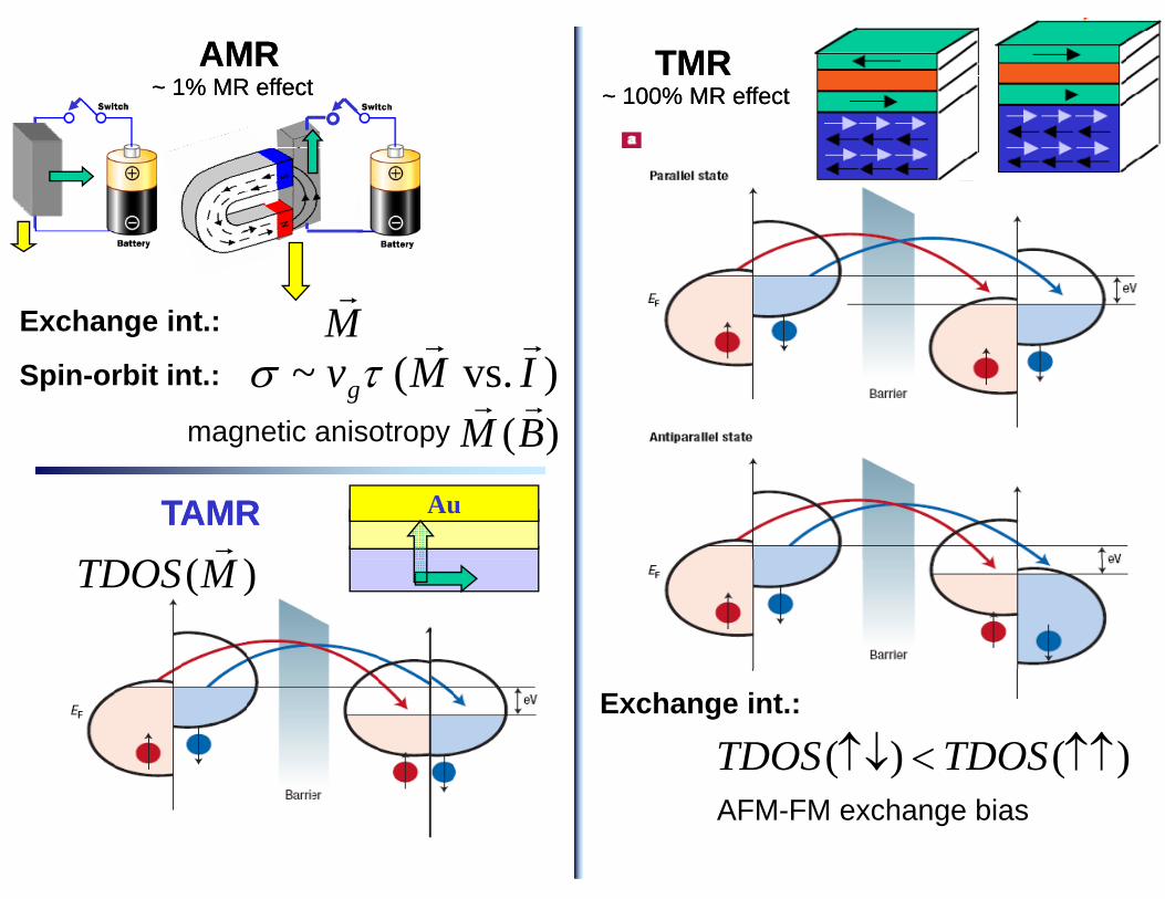
AMRAMR~ 1% MR effect~ 1% MR effect
Mr
Exchange int.:
) vs.( ~ IMvg
rrτσ
)(BMrr
Spin-orbit int.:
magnetic anisotropy
TAMRTAMR
)(
)(OSr
Au
)(MTDOS
TMRTMR~ 100% MR effect~ 100% MR effect
Exchange int.:
)()( ↑↑<↑↓ TDOSTDOS )()(AFM-FM exchange bias

TAMR in
ab intio theoryShick, et al, PRB '06, Park, et al, PRL '08
CoPt structures
experimentPark, et al, PRL '08
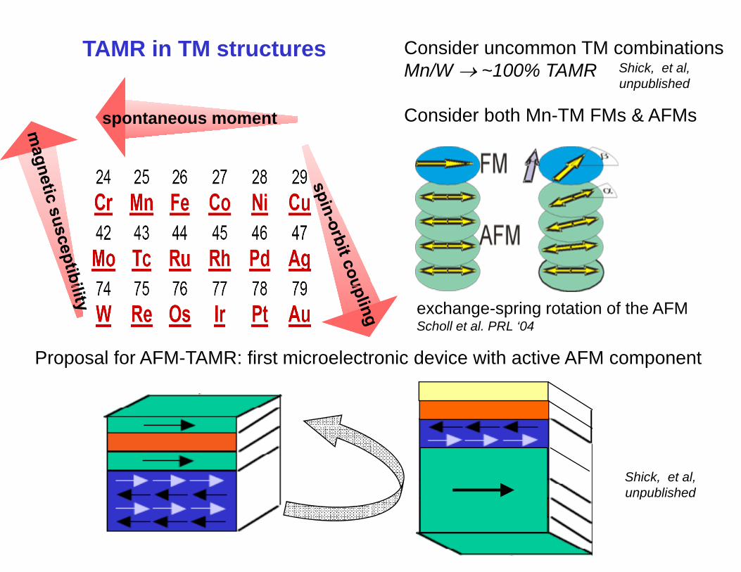
TAMR in TM structures
spontaneous moment
Proposal for AFM TAMR: first microelectrProposal for AFM-TAMR: first microelectr
Consider uncommon TM combinationsMn/W → ~100% TAMR Shick, et al,
Consider both Mn-TM FMs & AFMs
unpublished
exchange-spring rotation of the AFMScholl et al. PRL ‘04
ronic device with active AFM componentronic device with active AFM component
Shick, et al,unpublishedunpublished

OuOu
11.. Tunneling anisotropic magnetoresTunneling anisotropic magnetores
2 F ti i (G M )A2 F ti i (G M )A2. Ferromagnetism in (Ga,Mn)As an2. Ferromagnetism in (Ga,Mn)As an
3. Spintronic transistors3. Spintronic transistors3 Sp o c a s s o s3 Sp o c a s s o s
utlineutline
sistance in transition metalssistance in transition metals
d l t d i d td l t d i d tnd related semiconductorsnd related semiconductors

TM-based → semiconductinsensors & memories
Magnetic spintronic magp gmemories
Ferroelectrics/piezoelectrics
electro-mechanical transducors, large & persistent el. fields
ng multiferroic spintronics→ transistors & logicg
materialsgneto-sensors, g ,
Semiconductors
transistors, logic,sensitive to doping and p gelectrical gating

Ferromagnetic sNeed true FSs not FM inclusio
GaAs GaAs -- standard IIIstandard III--V semV sem
GG IIII MM dil tdil tGroupGroup--II II Mn Mn -- dilute dilute magnmagn& holes& holes
(Ga Mn)As(Ga Mn)As feferrromagnetiromagneti(Ga,Mn)As (Ga,Mn)As -- feferrromagnetiromagnetisemiconductsemiconduct
semiconductorsons in SCs
Ga
AsMn
miconductormiconductor
titi ttMn
As
eticetic moments moments
cccctortor

E↓
GaAs:Mn – extrinsi
EFspin ↓
1% M 1% Mn
DO
S << 1% Mn ~1% Mn
spin ↑As p like holes localized on Mn a
Asvalence band As-p-like holes
As-p-like holes localized on Mn a
As-FM due to p-d hybridization(Zener local-itinerant kinetic-exchange)
Mn-d-limom
ic p-type semiconductor
Energy
>2% Mn
gy
acceptorsonset of ferromagnetism near MIT
p like holesGa
Mn
acceptors
-p-like holesAs
Mn
ike localments

(Ga,Mn)As
L
H
high-T growth
H
→
Inco→
optimal-T growth
synthesis
ow-T MBE to avoid precipitation
High enough T to maintain 2D growthHigh enough T to maintain 2D growth
→ need to optimize T & stoichiometryfor each Mn-dopingfor each Mn doping
nevitable formation of interstitial Mn-donorsompensating holes and momentsp g→ need to anneal out

Interstitial Mn out-diffusiPolyscrystalline20% shorter bonds
OGaMnAs-oxide
GaMnAsMnI
++
10x shorther annealing with etch
O((is
ion limited by surface-oxide
x-ray photoemission
Olejnik et al, ‘08
Optimizing annealing time & temperature removing int Mn & keeping Mn in place)removing int. Mn & keeping MnGa in place) s essential Rushforth et al, unpublished
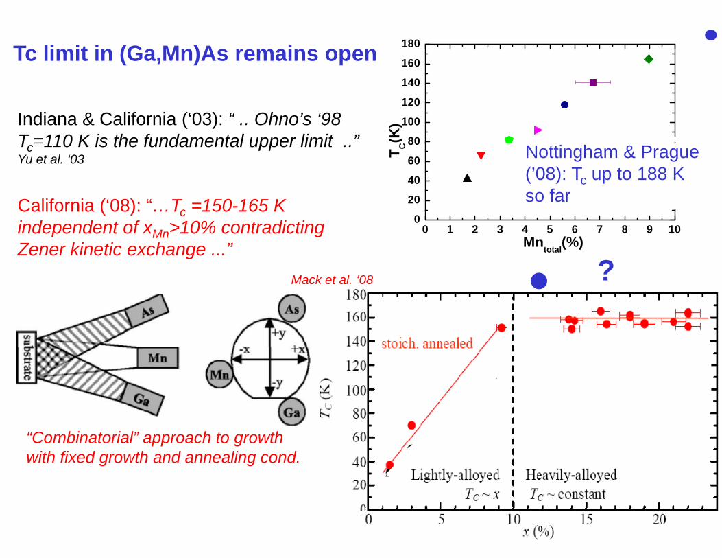
Tc limit in (Ga,Mn)As remains ope
Indiana & California (‘03): “ .. Ohno’s ‘98 T =110 K is the fundamental upper limit ”Tc 110 K is the fundamental upper limit .. Yu et al. ‘03
California (‘08): “…Tc =150-165 KCalifornia ( 08): …Tc 150 165 K independent of xMn>10% contradicting Zener kinetic exchange ...”
Mack et al ‘0Mack et al. 0
“Combinatorial” approach to growthwith fixed growth and annealing cond.
160
180
en
80
100
120
140
(K)
20
40
60
80
T C Nottingham & Prague (’08): Tc up to 188 Kso far
0 1 2 3 4 5 6 7 8 9 100
Mntotal(%)
?08 ?08
Mean-field butlow Tc
MF
Large TcMF but
low stiffness
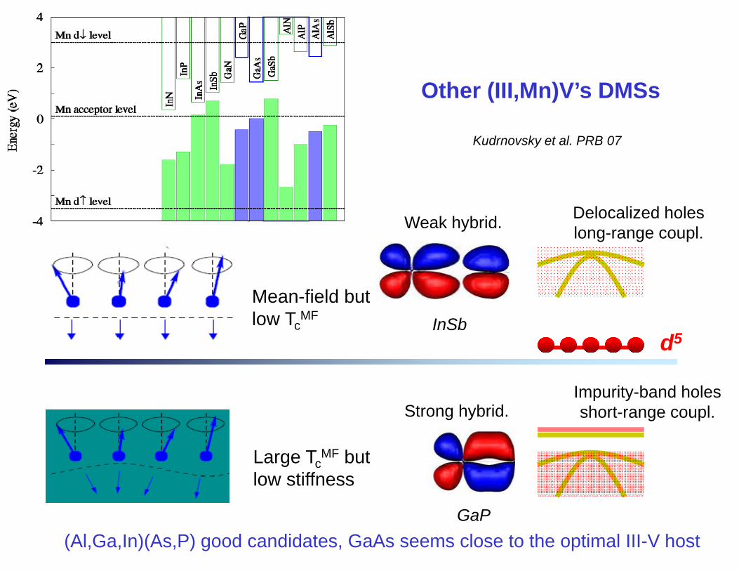
(Al,Ga,In)(As,P) good candidates, Ga
Other (III,Mn)V’s DMSs
Kudrnovsky et al. PRB 07
W k h b id Delocalized holes
y
Weak hybrid. Delocalized holeslong-range coupl.
InSbd5
t
Strong hybrid.Impurity-band holesshort-range coupl.
t
GaP aAs seems close to the optimal III-V host
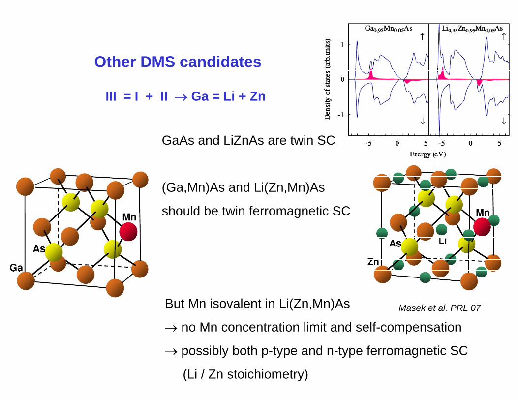
III = I + II → Ga = Li + Zn
Other DMS candidates
GaAs and LiZnAs
(Ga,Mn)As and L
should be twin fe
But Mn isovalent
→ no Mn concen
ibl b th→ possibly both
(Li / Zn stoich
n
s
s are twin SC
Li(Zn,Mn)As
erromagnetic SC
Masek et al. PRL 07t in Li(Zn,Mn)As
ntration limit and self-compensation
t d t f ti SCp-type and n-type ferromagnetic SC
hiometry)

Towards spintronics in (Ga,Mn)As
Dense-moment MSλ << dλF<< d↑-↑
Eu↑ - chalcogenides
Critical contribution to resistivity at Tc~ magnetic susceptibility magnetic susceptibility
s: FM & transport ↑
Dilute-moment MSλF~ d↑ ↑λF d↑-↑
Broad peak near Tc disappeares with annealing (higher uniformity)???annealing (higher uniformity)???

Critical contribution at
Fe
NiFisher & Langer ’68
dρ/dT ~ cv
Tc to dρ/dT like TM FMs
(Ga,Mn)As (Prague Nottingham)(Prague Nottingham)
Novak et al., ‘08
λF ~ d↑-↑

~),(~)( 2Γ JTRT pdi
rρ
⟩⟨Γ 2)(~ Suncor
rsmalluncor →Γ Tc
EuCdSe
MFΓ
χ~)0~~( FkkΓ
][ 00 ⟩⟨⋅⟩⟨−⟩⋅⟨ SSSS iid
rrrr
0=k1<<↑−↑kd
1~↑−↑kd
)/1~~( ↑−↑Γ dkk F
NivcdTddTd ~/~/ Γρ
Tc
Ferromagnetism & stroG
Mn
As-p-like holes
drdV
err
mcp
mcSeBH effSO
rrr
⎢⎣
⎡⎜⎝⎛×⋅⎟⎟
⎠
⎞⎜⎜⎝
⎛−=⋅−= μ (1
Strong SO due to the As p-shell (L=1) chara
Beff Bex + Beff
ong spin-orbit couplingGa
MAs
Mn
n
pss
LSrr rr
⋅=⎥⎦
⎤⎟⎠⎞ α)( ∇V
BBeffeff
ss
acter of the top of the valence band
BBeffeff
TAMR discovered in (Ga,Mn)As Gold et al. PRL’04

SCAMR in DMSs C
~
magnetic. only
~
>>max AMR
SO couped carries scattering coherently off Coulomb & polarized-magnetic potential of MnCou o b & po a ed ag et c pote t a o
MnGa
sign and magnitude (numerical) consistent with experiment

Remark: Extraordinary MRs & qua
dirty metal
ntum coherent transport phenomena
UCFUCF

OuOu
11.. Tunneling anisotropic magnetoresTunneling anisotropic magnetores
2 F ti i (G M )A2 F ti i (G M )A2. Ferromagnetism in (Ga,Mn)As an2. Ferromagnetism in (Ga,Mn)As an
3. Spintronic transistors3. Spintronic transistors3 Sp o c a s s o s3 Sp o c a s s o s
utlineutline
sistance in transition metalssistance in transition metals
d l t d i d td l t d i d tnd related semiconductorsnd related semiconductors

Gating of the highly doped
3]
1019
cm-3
dens
ity[
carr
ier
(Ga,Mn)As: p-n junction FET
10
]
p-n junction depletion estimates
6
8 0V 3V10
cm
2
4 5V 10V
dens
ity [
0.0 0.5 1.0 1.5 2.0 2.5 3.0 3.5 4.0
0
2ca
rrie
r
GaMnAs layer thickness [nm]
~25% depletion feasible at low voltages
Olejnik et al., ‘08

VV
Increasing ρ and decreasing AM
19.2
19.4
m]
V
18.8
19.0
19.2
ρ [1
0-3Ω
cm
20 22
18.6
1.02)
MR
098
1.00
B)/R
(B=0
)
AM
0.96
0.98
R(B
-400
Vg = 0VV 3V
MR, Tc, coercivity with depletion
24.0
24.5Vg = 3V
0
100
6 Ω
-100
0
230
23.5 -100
dρ/d
T [1
0-6
-200
100
24 26 28 30 32 34T [K]
22.5
23.0
20 22 24 26 28 30 32 34
-200
d
T [K]
-300
T [K] T [K]
Vg [V] -1.0
300
e] 0.0 1.0 2.0 2.530
200
250
e fie
ld [O
e
3.0 3.5
150
200
coer
cive
-200 0 200 400B [Oe]
-1 0 1 2 3 4Vg[V]

Persistent variations of magnetic p
200
65K62K depletionaccumulation
dR/d
T
100
d
30 40 50 60 70 80 90 100T (K)
properties with ferroelectric gates
Stolichnov et al., ,Nat. Mat.‘08
n
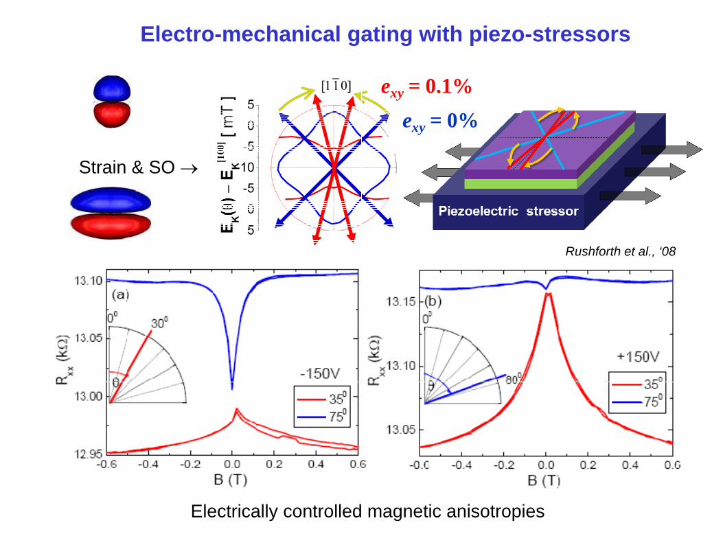
Electro-mechanical ga
Strain & SO →
Electrically controlled
ating with piezo-stressors
exy = 0.1%exy = 0%
Rushforth et al., ‘08
magnetic anisotropies

(Ga,Mn)As spintronic
Wunderlich et a
Huge, gatable, and
Single-electron transistor
Huge, gatable, and
single-electron transistor
al. PRL ‘06
d hysteretic MRd hysteretic MR
Two "gates": electric and magnetic

AMR nature of t
normal AMR
the effect
Coulomb blockade AMR

Single-electron charging ene
Source DrainVD
Q
GateVG
∫Q
'' M(Q)Q(VdQUr
μΔ
20 )QQ( r+
∫ +=0
D e(Q)Q(VdQU μ
MGG00 )]M(VV[CQ&
C2)QQ(U
Σ
+=+
=
electric && magnemagnecontrol of Coulomb blockade o
ergy controlled by Vg and M
QQindind = = nnee
QQindind = (= (n+1/2)n+1/2)eeQ0
Q0
ΔECe2/2CΣ
n-1 n n+1 n+2n-1 n n+1 n+2
)
C)M(μΔr
)[010]
Φ
M[110]
[100]
GM C
Ce
)M(V&)] ΣμΔ= [100]
[110][010]
eticeticoscillations
[0 0]
SO-coupling →μ(M)

Theory confirms chemical potenti& predicts CBAMR in SO-coupled& predicts CBAMR in SO coupled
al anisotropies in (Ga,Mn)Asd room-T metal FMsd room Tc metal FMs
•• CBAMRCBAMR ifif changechange ofof ||ΔμΔμ((MM)|)| ~~ ee22//22CCΣΣ
•• InIn ourour (Ga Mn)As(Ga Mn)As ~~ meVmeV (~(~ 1010 Kelvin)Kelvin)•• InIn ourour (Ga,Mn)As(Ga,Mn)As ~~ meVmeV (~(~ 1010 Kelvin)Kelvin)
•• InIn roomroom--TT ferromagnetferromagnet changechange ofof||ΔμΔμ((MM)|~)|~100100KK||ΔμΔμ((MM)|)| 100100KK
• Room-T conventional SET(e2/2CΣ >300K) possible(e /2CΣ 300K) possible
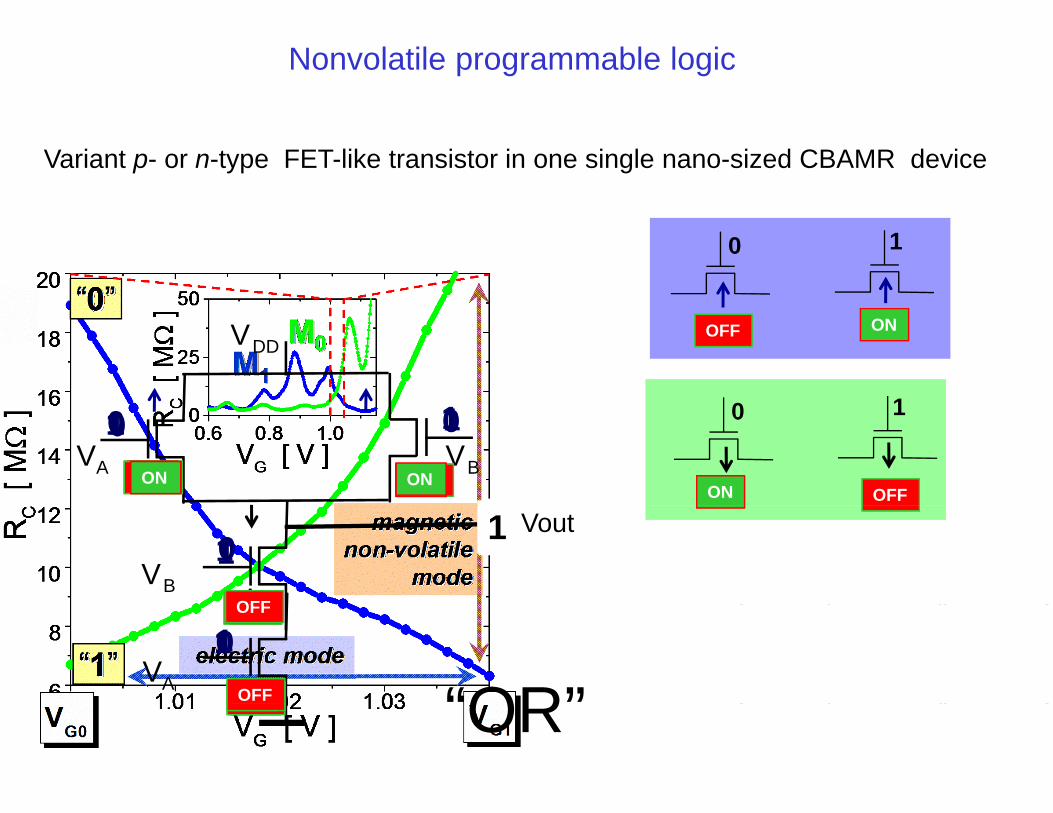
Nonvolatile progr
Variant p- or n-type FET-like transistor in
VDD
1VA VB
0 0OFFON OFF
1 0OFF
0ON
11ON
1ON
VB
V0
ON
0 01
OFF
1 11
OFF
1
VA
ON
01ONOFFON
0OFF
1OFF
OFF
“ORONOFF OR
rammable logic
one single nano-sized CBAMR device
0 1
ONOFF
0 10
ON OFF
1
Vout
A B Vout0 0 01 0 10 1 1R” 0 1 11 1 1
R

Nonvolatile progNonvolatile prog
Variant p- or n-type FET-like transistor in
VDD
VA VB
VB
V
VA “OROR
grammable logicgrammable logic
one single nano-sized CBAMR device
0 1
ONOFF
0 10
ON OFF
1
Vout
A B Vout0 0 01 0 10 1 1R” 0 1 11 1 1
R
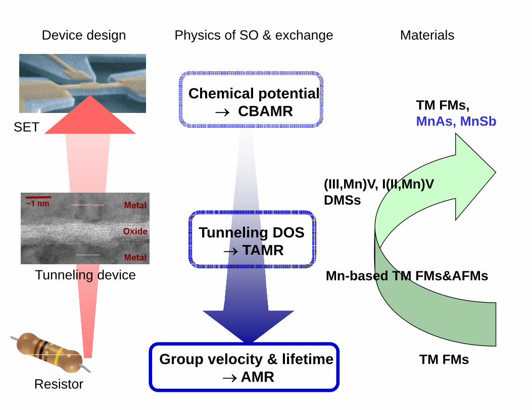
Physics of SO &Device design
Chemical pC
SET→ CBA
Tunneling→ TAM
Tunneling device
→ TAM
G l itResistor
Group velocity → AMR
& exchange Materials
potentialTM FMsAMR TM FMs,MnAs, MnSb
(III,Mn)V, I(II,Mn)VDMSs
g DOS MRMR
Mn-based TM FMs&AFMs
& lif ti TM FM& lifetime R
TM FMs