spin-polarized tunneling at interfaces between oxides and
TRANSCRIPT
Spin-Polarized Tunneling at Interfaces Between Oxides and
Metals or Semiconductors
by Douglas J. Strand
ARL-TR-3925 September 2006 Approved for public release; distribution is unlimited.

NOTICES
Disclaimers The findings in this report are not to be construed as an official Department of the Army position unless so designated by other authorized documents. Citation of manufacturer’s or trade names does not constitute an official endorsement or approval of the use thereof. Destroy this report when it is no longer needed. Do not return it to the originator.

Army Research Laboratory Aberdeen Proving Ground, MD 21005-5069
ARL-TR-3925 September 2006 Spin-Polarized Tunneling at Interfaces Between Oxides and
Metals or Semiconductors
Douglas J. Strand Weapons and Materials Research Directorate
Materials Division Materials Applications Branch
Approved for public release; distribution is unlimited.

ii
REPORT DOCUMENTATION PAGE Form Approved OMB No. 0704-0188
Public reporting burden for this collection of information is estimated to average 1 hour per response, including the time for reviewing instructions, searching existing data sources, gathering and maintaining the data needed, and completing and reviewing the collection information. Send comments regarding this burden estimate or any other aspect of this collection of information, including suggestions for reducing the burden, to Department of Defense, Washington Headquarters Services, Directorate for Information Operations and Reports (0704-0188), 1215 Jefferson Davis Highway, Suite 1204, Arlington, VA 22202-4302. Respondents should be aware that notwithstanding any other provision of law, no person shall be subject to any penalty for failing to comply with a collection of information if it does not display a currently valid OMB control number. PLEASE DO NOT RETURN YOUR FORM TO THE ABOVE ADDRESS.
1. REPORT DATE (DD-MM-YYYY)
September 2006 2. REPORT TYPE
Final 3. DATES COVERED (From - To)
5a. CONTRACT NUMBER
5b. GRANT NUMBER
4. TITLE AND SUBTITLE
Spin-Polarized Tunneling at Interfaces Between Oxides and Metals or Semiconductors
5c. PROGRAM ELEMENT NUMBER
5d. PROJECT NUMBER
5e. TASK NUMBER
6. AUTHOR(S)
Douglas J. Strand
5f. WORK UNIT NUMBER
7. PERFORMING ORGANIZATION NAME(S) AND ADDRESS(ES)
U.S. Army Research Laboratory Weapons and Material Research Directorate Materials Division, Materials Applications Branch (ATTN: AMSRD-ARL-WM-MC) Aberdeen Proving Ground, MD 21005-5069
8. PERFORMING ORGANIZATION REPORT NUMBER
ARL-TR-3925
10. SPONSOR/MONITOR'S ACRONYM(S)
9. SPONSORING/MONITORING AGENCY NAME(S) AND ADDRESS(ES)
U.S. Army Research Laboratory 2800 Powder Mill Road Adelphi, MD 20783-1197
11. SPONSOR/MONITOR'S REPORT NUMBER(S)
ARL-TR-3925 12. DISTRIBUTION/AVAILABILITY STATEMENT
Approved for public release; distribution is unlimited.
13. SUPPLEMENTARY NOTES
14. ABSTRACT
Spin-polarized tunneling is a way to create a new type of electric current whose two driving forces are spin momenta rather than opposite charges. Much research has been done with this idea and that research has been reviewed and developed to propose an experimental program to use this new type of current to devise such electronic devices as the Datta-Das spin field-effect transistor (SFET), the magnetic bipolar transistor, the hot-electron spin transistor, and the spin-valve photo-diode. This report includes a short history of spin-polarized transport and then outlines the developed theory. The experimental methods and materials of the field are also discussed. This research proposes to use electron paramagnetic resonance (EPR) and Barkhausen Noise Analysis (BNA) with other standard methods of materials science and engineering to examine the feasibility and develop an experimental plan to make spin-polarized transport effective for the manufacture of the above named devices. Some materials will be effective for spin-polarized transport devices and some will not. The quest for the effective materials is a major part of this research. Half-Heusler and full-Heusler alloys are studied as possible candidates for the devices. The term spintronics, an acronym for spin electronics, is used almost synonymously with spin polarization transport devices. 15. SUBJECT TERMS
Spintronics, spin polarization, spin injection, paramagnetic resonance,
16. SECURITY CLASSIFICATION OF: 19a. NAME OF RESPONSIBLE PERSON
Douglas J. Strand a. REPORT
U b. ABSTRACT
U c. THIS PAGE
U
17. LIMITATION OF
ABSTRACT
SAR
18. NUMBER OF PAGES
50 19b. TELEPHONE NUMBER (Include area code)
(410) 306-0827 Standard Form 298 (Rev. 8/98)
Prescribed by ANSI Std. Z39.18
Contents
List of Figures iv
1. Introduction 1
2. Problem Areas 4
3. Research Objectives 7
4. Recent Breakthroughs 8
5. Theory 8
6. Proposed Research Plan 13
7. Anticipated Results and Conclusions 25
References 33
Acronyms 36
Bibliography 38
Distribution List 39
iii
List of Figures
Figure 1. Full Heusler alloy with L21 structure............................................................................... 5 Figure 2. Half-Heusler alloy with C1b structure. ............................................................................ 6 Figure 3. The basic principle of MBE showing coevaporation of atoms or molecules from
two different sources onto a heated substrate. ........................................................................ 16 Figure 4. Heterojunction , with dangling bonds at the interface, of a lattice mismatched 3-D
crystal...................................................................................................................................... 16 Figure 5. Spin-valve photo-diode (48).......................................................................................... 29
iv
1. Introduction
It was shown in the 1970s that the spin conservation in electron tunneling gives rise to the possibility of spin sensitive tunneling between two ferromagnetic films. One example is the study of the interface of iron (Fe) and nitrogen (Ni) with aluminum oxide (Al2O3) in Fe / Al2O3 / Ni. This is an example of a FM/I/FM junction, where FM stands for ferromagnetic and I stands for insulator. The current technique of forming Al2O3 barriers is by oxidizing a thin aluminum (Al) layer deposited on the ferromagnet.
X-ray Photoelectron Spectroscopy (XPS) can be used to characterize the compositional, chemical, and electronic properties of this system. These properties can then be correlated to other properties of the interface, such as magnetoresistance (MR). MR is the increase in the electrical resistance of a metal or semiconductor when placed in a magnetic field. The analysis of the experimental results on MR bears directly on the shape and connectivity of the Fermi surface. Transverse MR is of greatest interest. Using an (x,y,z) Cartesian coordinate system, x is the direction of transport and of the applied electric field; z is the direction of the applied magnetic field; and y is called the transverse direction and is the direction of the Hall field.
The most interesting experiments are those carried out at low temperatures on very pure specimens in strong magnetic fields, since under these conditions the product τω c of the cyclotron frequency and the relaxation time may be 1. Also under these conditions, the details of the collision processes are suppressed and the details of the Fermi surface enhanced. The effect of a weak magnetic field
ff
( )1ppτωc is to increase the resistance by an additive term proportional to H2.
In very strong fields, when 1ffτωc , the transverse MR of a crystal may generally do one of three things: saturate, continue to increase, or saturate in some crystal directions but not in others. Crystals are known in all three categories. The first category consists of crystals with closed Fermi surfaces, such as indium (In), Al, sodium (Na), and lithium (Li). The second category consists of crystals with equal numbers of electrons and holes, such as bismuth (Bi), antimony (Sb), tungsten (W), and molybdenum (Mo). The third category consists of crystals with Fermi surfaces having open orbits for some directions of the magnetic field, such as copper (Cu), silver (Ag), gold (Au), magnesium (Mg), zinc (Zn), cadmium (Cd), gallium (Ga), thallium (Tl), tin (Sn), lead (Pb), and platinum (Pt). The value of MR tells us whether the Fermi surface is closed or contains open orbits, and in which directions the open orbits lie. The transverse MR does not saturate if there are equal numbers of holes and electrons.
It is remarkable that in some crystals the MR saturates except for certain special crystal orientations. This can be explained in terms of open orbits, which occur in strong magnetic fields. An orbit is open if it carries current essentially only in a single direction in the plane normal to the magnetic field. Therefore, the open orbit cannot be saturated by the field. It has been shown that the MR saturates except when the open orbit carries current almost precisely parallel to the y direction, i.e., the direction of the Hall electric field. This explains the extraordinary anisotropy of the transverse MR observed in single crystals. (1)
1
Quantized energy levels or the interaction of quantized spins create quantum functionality. Contemporary materials engineering techniques now enable the fabrication of a wide variety of compositionally modulated materials, which are commonly called “heterostructures.” These heterostructures have excellent control of explicitly quantum mechanical phenomena such as quantum confinement and quantum tunneling. They have had a lasting impact on quantum device technologies as well as on fundamental discoveries in condensed matter physics. For example, semiconductor heterostructures play an important role in contemporary opto-electronics and microwave frequency devices, while also providing a rich arena for examining correlated electron physics in low dimensions.
At the same time, advances in the fabrication of metallic magnetic heterostructures now allow us to read memory of unprecedented density with the giant magnetoresistance (GMR) effect and also form the basis for a nonvolatile memory know as “magnetic random access memory” (MRAM). MRAM uses magnetic hysteresis to store data and MR to read data. In addition to the nonvolatility of MRAM, other advantages include much faster write times, no wearout with write cycling, lower energy for writing, and access times that are about 1/10,000 of those of hard disk drives.
Galvanic isolators are another application of spin electronics (spintronics) (2). These advances have led to the integration of the fields of semiconductor heterostructures and magnetic materials to create the new field of “semiconductor spintronics” that ties these usually disparate areas of science and technology (3).
Nanostructures are another class of materials that are important to spintronics. Transport experiments have been performed on ferromagnetic (Ga,Mn)As* nanoconstrictions that can be used to trap and investigate domain walls, which can, in turn, be used to study spin injection. (4)
The effect of spintronics on technology can only be speculated. Moore’s Law may give us an idea of the magnitude of its impact. It states that microprocessors will double in power every 18 months as electronic devices shrink and more logic is packed into every chip (5).
The Chambers or kinetic formulation of the transport equation is more revealing for the MR problem with a general Fermi surface than is the common iterative Boltzmann method, where magnetic effects appear only in second order. The most useable transport equation for MR is the general nonlinearized result of Chambers, which for the distribution function is
( )( ) ( )( ) ( )( )∫ ∞− ⎟⎟⎠
⎞⎜⎜⎝
⎛⎟⎟⎠
⎞⎜⎜⎝
⎛−Δ−=
t
t skdstftk
dtf'0 exp''
'τ
εετ ∫t
, (1)
where is the energy gain from the force F between times t’ and t in the
absence of collisions;
( )∫ ⋅=Δt
ttvFdt
'''''ε
τ is the relaxation time; and is the equilibrium distribution function. This leads to the fact that there is always a longitudinal MR that always saturates. For
0fTkBc fω
and 1ffτωc , an oscillatory behavior is observed in the conductivity components. The quantum
*Ga = gallium, Mn = manganese, and As = arsenic.
2

oscillations in transport properties have the same origin as the susceptibility oscillations in the de Haas-van Alphen effect (1).
There are two types of MR, anisotropic magnetoresistance (AMR) and GMR. AMR measures the change in resistance seen when the current flowing through a sample changes from being parallel to the internal magnetization to being perpendicular to it. AMR is applicable to single-crystal magnetic metal whiskers, but the discovery of GMR brought a new class of magnetoresistive systems into being. GMR is a term coined to describe the behavior of materials consisting of alternating layers of ferromagnetic and nonmagnetic metals deposited on an insulating substrate. The GMR effect is the phenomenon that the resistance, measured by current flowing parallel to the layers (of constant thickness) in multilayered metallic film structures, is greatest when the magnetic moments in the alternating layers are oppositely aligned and smallest when they are all parallel. This change was found to be 100% in the original experiments reporting GMR, while the most recent record is 220% at low temperatures. The largest effects are seen with Fe-chromium (Cr) or cobalt (Co)-Cu alternating layers up to approximately 100 repeats at layer thicknesses of a few nanometers. (6)
These developments led to the field of spintronics. The goal of spintronics is to understand the interaction between a particle’s spin and its solid-state environments, and to make useful devices using the acquired knowledge. The common goal in many spintronic devices is to maximize the spin detection sensitivity to the point that it detects not the spin itself, but changes in the spin states (7). The use of electron spin offers the potential advantages of nonvolatility, lower power consumption, increased data processing speed, and increased integration densities compared with conventional semiconductor devices (2).
To compare spin current to charge current, we start by calling density spin polarization a and current spin polarization b. Then, b is the ratio of spin current js, which is the difference between the charge currents formed by the spin-up and spin-down electrons and the total charge j:
jj
b s= . (2)
The current spin polarization is much less intuitive than the density spin polarization. There are several reasons for this. First, b involves not only the carrier and spin densities, but also the drift or diffusion velocities, which can be spin dependent. Second, unlike a, the magnitude of b is not restricted to a small interval. The magnitude of b is not even bounded. Therefore, the spin current can be finite even if there is no charge current, making b infinite. In addition, the signs of b and a can be different. Third, unlike the charge current, the spin current need not be uniform. Because of spin relaxation, js (and also b) is not conserved. For these reasons, unless the relation between a and b is obvious or is explicitly derived, b is not indicative of the spin injection efficiency. (8)
In addition to XPS, electron paramagnetic resonance (EPR) spectroscopy can be used to characterize the properties. Electronic paramagnetism exists when the atoms or molecules in a substance possess a net electronic magnetic moment. There are four types of substances that exhibit paramagnetism (9):
1. All atoms and molecules that have an odd number of electrons
2. All free atoms and ions with unfilled inner electron shells and many of these ions when in solids or in solution
3
3. Several miscellaneous compounds, including molecular oxygen and organic biradicals
4. Metals
When a variable magnetic field is applied to such a material, resonance occurs when the frequency of this applied field is equal to the frequency of the magnetic field created by the atoms’ (molecules) electronic magnetic moment. An EPR spectrometer works off this principle and provides a spectrum that can be interpreted to characterize the substance. The results of the two methods, XPS and EPR, will be compared and contrasted to obtain a further understanding of the properties of the interface, because each method complements the other by giving a different perspective of the material.
2. Problem Areas
An ideal spintronic material would be one that enables the transport of only one spin carrier across the interface between it and an unpolarized material, without any spin-flip scattering. This project will attempt to find such an ideal spintronic material. Epitaxial (having a semiconductor layer grown from a substrate layer) Heusler alloys are considered to be prime candidates, because they show great potential for spin-injection contacts to compound and elemental semiconductors. The Heusler structures consist of four interpenetrating face-centered-cubic (fcc) sublattices with atoms at X1(0,0,0), X2(½,½,½), Y(¼,¼,¼), and Z(¾,¾,¾), some of which may or may not be filled. In the full Heusler alloy, X2YZ with the L21 crystal structure, all of the sublattices are filled. A drawing of this is shown in figure 1.
4
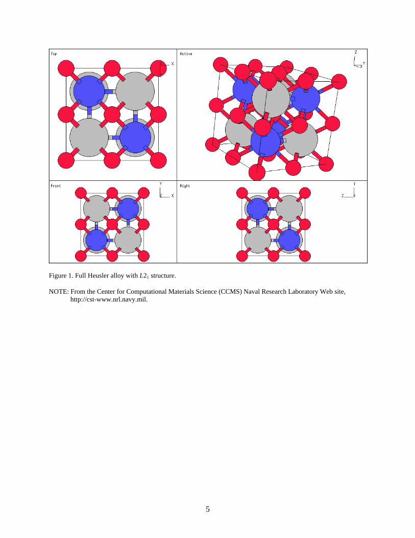
Figure 1. Full Heusler alloy with L21 structure.
NOTE: From the Center for Computational Materials Science (CCMS) Naval Research Laboratory Web site, http://cst-www.nrl.navy.mil.
5
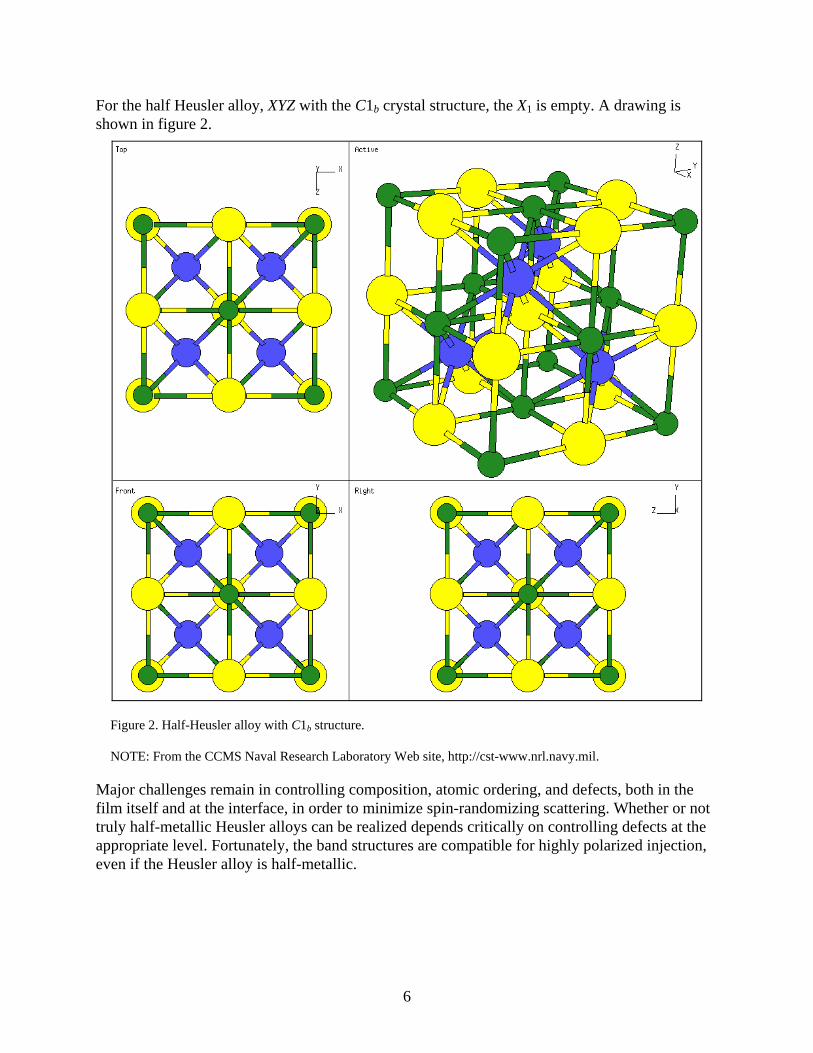
For the half Heusler alloy, XYZ with the C1b crystal structure, the X1 is empty. A drawing is shown in figure 2.
Figure 2. Half-Heusler alloy with C1b structure.
NOTE: From the CCMS Naval Research Laboratory Web site, http://cst-www.nrl.navy.mil.
Major challenges remain in controlling composition, atomic ordering, and defects, both in the film itself and at the interface, in order to minimize spin-randomizing scattering. Whether or not truly half-metallic Heusler alloys can be realized depends critically on controlling defects at the appropriate level. Fortunately, the band structures are compatible for highly polarized injection, even if the Heusler alloy is half-metallic.
6
Gardelis et al. (2) have attempted to produce the ternary half-Heusler alloy NiMnSb as a bulk material with very good properties for spintronics using arc welding. This material has been used as a target to grow highly crystalline NiMnSb thin films on semiconductor substrates at low temperatures of approximately 200 °C by pulsed laser deposition (PLD). NiMnSb crystallizes in the C1b structure. This structure consists of four interpenetrating fcc superlattices equally spaced along the (1,1,1) direction. Ni occupies the lattice site at (0,0,0). Mn occupies the site at (¼, ¼, ¼). The site at (½, ½, ½) is unoccupied and, lastly, Sb occupies the site at (¾, ¾, ¾). The magnetic properties are due to magnetic moments localized at the Mn atoms, which interact by itinerant electrons. It has been shown that 9 out of 22 valence electrons are located in spin-down bands; therefore, the total spin magnetic moment of NiMnSb becomes 4.0 µb, i.e., an integral number as expected for half-metallic ferromagnets. All the properties of NiMnSb that were investigated by Gardelis et al. (2) indicated that at a temperature of approximately 150 K there is a crossover from half-metallic to normal ferromagnetic behavior. They also demonstrated that PLD could be used for low-temperature deposition of highly crystalline thin films of this material (2). In addition, spin-injection polarization measurements for transport from a Heusler alloy into a semiconductor are anticipated in the near future, utilizing spin-light emitting diode (LED) structures (10).
Magnetic tunnel junctions with a stacking structure of Cr/Co-Mn-Al/Al-O/Co-Fe/Ir-Mn2 were fabricated using an ultra-high vacuum (UHV) magnetron-sputtering machine. The Co-Mn-Al films showed a B2 structure, which involves partial disorder between Mn and Al sites. Tunnel magnetoresistance (TMR) ratios at room temperature were 27% and 40% before and after annealing at 250 °C, respectively. Those values are much higher than the ones obtained in previous experiments using half Heusler alloys. Optimization of sputtering and oxidation conditions can further enhance the TMR ratios. Furthermore, a high spin polarization material can engender a large TMR. Since Co2MnAl was found to have such a high spin polarization, this alloy is very promising for future applications. (11)
3. Research Objectives
The objective of this research will be to develop arrays of individual magnetic memory cells in which the data is stored as the direction of magnetization of very small ferromagnetic elements. A multiplexed current pulse technique to reverse selected magnetic elements will be used for the writing process, while a tunneling MR technique will be used for the read process (12).
2O = oxygen and Ir = iridium.
7
4. Recent Breakthroughs
The potential impact of this research is that information can be stored in a new and more efficient way in communications and computer systems. The energy within the spins of electrons can be directed to produce faster and more controlled systems. The carriers of current in a ferromagnetic metal, such as Fe, Co, or Ni, are themselves magnetically polarized. The magnetic moments of these carriers reflect an imbalance between up and down spins. A normal metal, such as Cu, has equal numbers of electrons with up and down spins, and hence have no net moment. These electrons, which are at the top of the filled states (Fermi level), are unpolarized. However, a ferromagnetic metal, to avoid the high energy of having a high density of states at the Fermi level, has a splitting between the up and down spin states, called “exchange splitting,” which lowers the total energy of the system. Here, there is a spin imbalance with the up-spin (or majority) d-electron states all filled and the d-electron states at the Fermi level containing entirely down-spin (minority) electrons. The moment of the atom is simply proportional to the difference between the number of spins in the two spin bands. At the Fermi level, the carriers can be s, p, or d shell electrons. The d electrons are more highly polarized than the s or p electrons and produce a current that is partially spin polarized (6, p. 58). This concept of spin polarization will be studied and applied to data storage in this project.
5. Theory
The theoretical models of junction magnetoresistance (JMR) will be examined for their correctness and applicability using modern technology. Julliere’s formula will be studied for its applicability, along with Slonczewski’s model. One critical issue will be determining which theoretical model provides the truest picture of spin-polarized tunneling as applied to ferromagnetic junctions (13).
The early theories of JMR were based on a number of simplifying assumptions. Specifically, they usually employ simple parabolic bands and/or momentum and energy independent tunneling matrix elements. The classical theory of tunneling assumes that the left and right electrodes are two completely independent systems and the insulating barrier is a perturbation permitting quantum tunneling between them. In a tunnel junction, the relative change in the resistance of the junction is given by
RL
RLTMR PP
PPR+
=12
, (3)
where PL and PR are the spin polarizations of the left and right electrodes, respectively. This is Julliere’s formula.
Slonczewski’s model treats the ferromagnetic/barrier interface more realistically than Julliere’s classical theory of tunneling. He considered the electrodes and the barrier to be a single quantum mechanical system; however, each electrode has an evanescent wave function of electrons that
8
penetrate into the tunnel barrier. Slonczewski recognized that these wave functions need to be matched across the junction. His principal result was that the polarization P of tunneling electrons depends on the height of the barrier, Vb, through an imaginary wave vector, κi , in the barrier defined by
( )[ ] 2/12 Fb EVm −=κh , (4)
which is
↓↑+↓↑−
↓+↑↓−↑
=kkkk
kkkkP 2
2
κκ , (5)
where are the Fermi wave vectors in the up- and down-spin bands. (In a three-dimensional (3-D) crystal, modes may propagate in any direction and the wavenumber k becomes a vector
↓↑ kk ,
κ . It is limited to a Brillouin zone. For each wavenumber, there are three acoustical modes.)
For a high barrier, the polarization P reduces to Julliere’s formula, but P can even change sign when the barrier is low (13). A problem that was encountered with the Slonczewski model was that the method of matching the wave functions is not easily generalizeable beyond a simple parabolic band. For this reason, most recent theories of JMR are based on the versatile and rigorous Kubo/Landauer formula for conductance. In this formula, the total conductance Gσ in a spin channel σ can be expressed in terms of the one-electron Green’s functions
. Here L and R represent the left and right neighboring planes of the junction and is the electron momentum parallel to the junction. The formula is
( ) ( 1111 ,,, kEgkEg FRFLσσ )11k
( )[ ] ( )[ ]( )∑ ⋅=11
1111
2
,Im,Im4k
FLt
FR kEgTkEgTTrheG σ
σσ
σσ , (6)
where , and represent matrices in the orbital space, and the imaginary part of the Green’s function represents the density of states for the system.
11,, kgg RLσσ
σT
The summation is over the two-dimensional (2-D) Brillouin zone and the trace is over the orbital indices corresponding to (s,p,d) orbitals, which are required in a tight-binding parameterization of the electrodes and the barrier. The matrix, , is given by σT
, (7) ( ) ( ) ( ) ( ) ( )[ ] 11111111111 ,, −
−= ktkEgktkEgIktT FLt
FRσσ
σ
where I is a unit matrix in the orbital space and ( )11kt is the matrix of tight-binding hopping integrals connecting atomic orbitals in the left and right planes between which the tunneling current is calculated.
The Kubo/Landauer formula can be used to describe coherent tunneling, i.e., conservation of the momentum parallel to the junction, or noncoherent tunneling. There are two categories of noncoherent tunneling: either disorder is simplified and band structure is realistic, or it is the other way around and band structure is simplified and disorder is realistic. The simplest treatment of disorder in the barrier is provided by the classical theory of tunneling, i.e., Julliere’s formula, which assumes that tunneling from any occupied state of the left electrode to any
9
unoccupied state in the right electrode is equally probable. This model has two problems. First, it leads to an incorrect sign of the tunneling current, and second, it fails to describe JMR in junctions with a nonmagnetic metallic interlayer. Julliere’s formula can be corrected by examining the approximations that must be made to derive it from the Kubo/Landauer formula.
The generalization of Julliere’s formula incorporating all of the corrections resulting from the approximations takes the form
( ) ( )[ ] ( ) ( )[ ]∑∑ ×=' '
11'
1111
2
'1111
,Im0,Im04k FL
tk FR kEgtkEgtTr
hNeG σσσ , (8)
where the prime indicates that all the quantum well states are excluded and the trace is again over all the orbital indices. Quantum well states are bound states that are formed in junctions with a nonmagnetic metallic interlayer and do not contribute to transport of charge. This generalized Julliere’s formula is the simplest physically plausible description of tunneling in the presence of disorder. Disorder is the degree to which the tunneling is not coherent, i.e., the degree to which the momentum, , parallel to the junction, is not conserved. 11k
Two additional effects are the Coulomb blockade effect and the enhancement of the JMR in the Coulomb blockade regime, which apply when a small grain of a ferromagnetic material is separated by insulating barriers from ferromagnetic leads. In this case, tunneling to the grain may be strongly influenced by the charging energy in the grain. For a very small grain, the electrostatic energy increases by
C
e2
2
(9)
when an electron tunnels into the grain (e is the electron charge and C is the capacitance of the grain). Tunneling is, therefore, blocked unless the charging energy is overcome by bias voltage or thermal energy. This effect is the Coulomb blockade effect.
The second effect is an enhancement of the JMR in the Coulomb blockade regime for a double junction explained by the fact that there is an absence of Coulomb blocking in small grains resulting in sequential tunneling (two independent tunneling effects) at high temperatures and co-tunneling (a coherent tunneling through both junctions via a virtual intermediate state) at low temperatures. For sequential tunneling, the effective resistance of a double junction is proportional to the sum of the resistances of the two junctions, whereas, for co-tunneling, the total resistance is proportional to the product of the junction resistances.
The conductance G(Hs) of a tunnel junction with two ferromagnetic electrodes, whose magnetic moments are aligned parallel in an applied saturating field Hs, is much higher than its conductance G(0) in zero field when the moments are antiparallel. This is called tunneling JMR and the relative change in the resistance of the junction, i.e., the so-called JMR ratio, is defined as
1
11
)0()()0(
−
−− −=
GHGG
JMR S . (10)
10
Looking at the ratio of the resistances at low temperatures, the JMR ratio is enhanced, but it reverts to the usual bulk JMR ratio at high temperatures. Extending these ideas provides an explanation of an enhancement of the JMR observed in granular systems at low temperatures (13, pp. 261–7, 270).
The field of spintronics can be divided into two categories: those that cover the emerging applications and those covering already well-established schemes and materials. The second group is also called magnetoelectronics and typically covers paramagnetic and ferromagnetic metals and insulators that utilize MR effects. Examples are magnetic read heads in computer hard drives, nonvolatile MRAM, and circuit isolators. There is a large class of emerging materials that characterize the first category of spintronics. Examples are ferromagnetic semiconductors, organic semiconductors, organic ferromagnets, high-temperature superconductors, and nanotubes. These materials can bring novel functionalities to the traditional devices (7, p. 325). We will look at the first category in this study, because we want to examine the usefulness of EPR and Barkhausen Noise Analysis (BNA) with these materials, but we also want to investigate some of the emerging materials as the promise of their usefulness is very great.
The occurrence of ferromagnetism in magnetic semiconductors is neither a new nor rare phenomenon, and was extensively studied several decades ago in materials such as manganites, semiconductor spinels (e.g., CdCr2Se43), the europium chalcogenides (e.g., EuO), and the lead chalcogenides (e.g., Pb1-x-ySnyMnxTe4). The recent resurgence of interest in ferromagnetic semiconductors has largely been ignited by the discovery of ferromagnetism in the Mn-doped III-IV semiconductors, Ga1-xMnxAs and In1-xMnxAs.
Mean field theories developed to understand the origins of ferromagnetism in the III-Mn-V semiconductors have lead to predictions of ferromagnetism in a much wider class of magnetically doped semiconductors. In addition to the mean field approach that relies on carrier-mediated ferromagnetism, first principles calculations have also predicted the existence of ferromagnetic ground states in many different materials. These predictions have created intense interest in the crystal growth of magnetic semiconductors such as (Zn,Cr)Te, magnetic III-V nitrides, phosphides, antimonides, magnetic group IV semiconductors, and various other complex phosphides and oxides.
Magneto-transport in Ga1-xMnxAs will be examined in this project. Magneto-transport measurements in III-Mn-V ferromagnetic semiconductors provide a convenient means of probing the ferromagnetic properties. The Hall effect in these materials has contributions from both the standard Hall voltage and the “anomalous Hall effect” (AHE) and is described by
MRBR AHxy 0μρ += , (11)
where RH is the ordinary Hall coefficient, RA is the AHE coefficient, and M is the sample magnetization. A detailed understanding of the AHE in Ga1-xMnxAs is relatively recent, wherein the AHE originates not in the interplay between spin-orbit coupling and elastic scattering, but rather from an intrinsic Berry’s phase effect related to the presence of the spin-orbit coupling
3Se = selenium. 4Te = tellurium.
11
itself. Berry’s phase effect is the phenomenon that any “vector” that is parallel-transported (moved keeping the same direction) along a path back to the original place may acquire an angle with respect to its initial direction prior to transport. This angle is a geometric property. (14)
This theory also addresses all aspects of the anisotropic magnetoconductivity tensor in these ferromagnetic semiconductors. An interesting consequence of this anisotropic magnetoconductivity tensor is the “planar Hall effect,” wherein a transverse electric field arises in a measurement geometry identical to that used for AMR (see section 1) measurements (i.e., the magnetic field is in plane). While this planar effect is very small in metallic ferromagnets, it is extremely large in Ga1-xMnxAs. This “giant planar Hall effect” is an elegant and sensitive probe of the angle-dependent magnetization and also provides a means of studying magnetic domain reversals. Quite remarkably, the large domain sizes in Ga1-xMnxAs enable the observation of Barkhausen jumps (small discontinuities in the magnetic hysteresis loop caused by domain wall movements (15)), even in devices as large as a few microns. Ongoing measurements of this planar Hall effect show that the signals tend to be even larger in more insulating digital Ga1-xMnxAs alloys. The Barkhausen jumps will be examined in this project using a Stressscan 5000 instrument.
Since one of the main goals of semiconductor spintronics is to obtain optical or electrical control of ferromagnetism, it is important to identify ferromagnetic semiconductors wherein there exists a clear coupling between the carrier density and ferromagnetic order. The best way to do this is to carry out multiple complementary measurements that probe the ferromagnetic transition. Some of the common tools that can be used to obtain these measurements are the anomalous Hall effect, magnetic circular dichroism, temperature-dependent conductivity, magneto-optical Kerr effect, and superconducting quantum interference device (SQUID) magnetometry. (3)
Magnetic domains, and the boundaries that separate them (domain walls (DWs)), play a central role in the science of magnetism. Understanding and controlling domains is important for many technological applications in spintronics and may lead to new devices. Negative intrinsic resistivity of an individual domain wall in epitaxial (Ga,Mn)As microdevices have been studied. Steady and pulsed magnetic fields have been applied to trap and carefully position an individual DW within each separate device studied. This procedure reproducibly enables high-resolution MR measurements across an individual wall. Negative intrinsic DW resistance that scales with channel width has been consistently observed. This appears to come from sizeable quantum corrections to the MR. Precise extraction of the domain wall resistance (DWR) can be achieved by averaging the measured longitudinal resistances,
( ) 2/Dxx
Uxx RRR += , (12)
which compensates obscure contributions from the transverse voltages. The difference between R and
( )A
LtR0
0 ρ= , (13)
a simple, idealized prediction for the longitudinal resistance, clearly displays the presence of effects beyond those associated with a simple resistivity discontinuity at the DW.
12
There are two fundamental contributions to this difference called the “eddy-like” and “intrinsic” DW resistivities. To date, the experimental results obtained from the various methods are conflicting. Both positive and negative DWRs are reported. There are several scattering mechanisms that can produce positive DWR, including reflection of carriers by the DW, a “zigzag” current redistribution inside the wall due to the Hall effect, and spin-dependent scattering analogous to the GMR effect in magnetic layers. Negative DWR could possibly arise from electronic coherence in ferromagnetic metals. This could be due to the suppression of dephasing of weakly localized electrons at a DW, effectively reducing the intrinsic resistivity of DWs. In addition, a semiclassical model has been developed that can theoretically yield either positive or negative DWR. (16)
6. Proposed Research Plan
There have been essentially nine sets of experiments performed in this area. In the first set, contacts were normal metals and current was passed through “spin filters,” which are barriers whose conductance depends on spin (17). The second was the first to measure the spin polarization of the current originating in a ferromagnetic metal film. In these experiments, electrons tunneled through a nonmagnetic insulating barrier film into a superconducting metal film that acted as a “spin polarized” detector when a magnetic field, H, was applied to the structure (18). In the third, instead of analyzing the spin polarization of the tunneling current using a superconducting film in an applied field, experimenters replaced the superconducting film with another ferromagnetic metal film (19). The next three sets of experiments dealt with how spins interact. They interact mainly through spin coupling and spin-orbit coupling. If these influences could be eliminated, the orientation of a carrier’s spin can last a long time.
The context of the fourth set of experiments was the excitation of a non-equilibrium population of spin-polarized electrons in the skin depth of a normal metal when microwave radiation is absorbed in an electron-spin resonance experiment, and the diffusion of these electrons from the skin into the bulk of the metal. A spin diffusion length was defined such that the generated spin imbalance would relax over it. This length was
ss DL τ= , (14)
where D is the electron diffusion constant and sτ is the spin relaxation time. The fifth set of experiments measured this spin diffusion length directly through a transport experiment, using ferromagnetic metal contacts to inject spins into a normal metal (20). The sixth experiment measured the spin diffusion length of carriers injected into a paramagnetic metal from a ferromagnetic contact (21).
The seventh set of experiments tested the dependence of the GMR effect (stated on page four) on the relative orientation of moments in simple sandwich structures consisting of two ferromagnetic layers separated by a normal metal. They showed that the GMR affects scales simply as the projection of the magnetic moment of one layer upon the magnetic moment of the other (22, 23). The resistance derives from electron scattering events that are spin defined (24). These events fall into two categories: spin-defined scattering at interfaces where the films meet and spin scattering within the interior (bulk) of the films. The eighth set of experiments
13
attempted to identify which of these categories is more important. They indicated that for homogeneous layers the spin scattering is primarily at the interfaces. This was done by inserting thin layers of a second ferromagnetic material at the interfaces in ferromagnetic/nonmagnetic/ ferromagnetic sandwiches. It was generally observed, for many different combinations of metals that the MR varies exponentially on the thickness of the interface layer, with a characteristic lengthξ . It was found that lengthξ was extremely short and was typically ≈1.5 to 3 Ǻ at room temperature, and thatξ became even shorter at lower temperatures. The GMR effect was thus clearly shown to be determined by the character of the ferromagnetic/nonmagnetic interfaces (25); however, magnetic defects within the interior of a film, such as magnetic impurities in the nonmagnetic metal layer or inhomogeneities within the ferromagnetic layer, can also contribute measurable spin scattering.
In this project, I will demonstrate, by the insertion of thin magnetic layers at the interfaces in sandwich structures, that the magnitude of the GMR effect is determined largely by the character of the magnetic/nonmagnetic interfaces. These magnetic layers can be inserted between any magnetic and nonmagnetic layer and will be approximately 2.5 Ǻ thick. It has been show that “dusting” a nonmagnetic/magnetic interface with thin Co layers, just 2.5 Ǻ thick, almost doubles the MR of the nonmagnetic/magnetic/nonmagnetic sandwich, making it comparable to the sandwich in which the nonmagnetic layers are completely replaced by Co. The thickness dependence is well described by a function of the form
⎥⎦
⎤⎢⎣
⎡⎟⎟⎠
⎞⎜⎜⎝
⎛ −−+=
Δξ
itba
RR exp1 , (15)
where the length scaleξ is extremely short and is only ≅2.3 Ǻ (25, p. 1642). This relates well to the EPR part of this project, because spin injection (what EPR measures) and MR (what is being examined here) both relate to an understanding of spintronics.
The samples will be prepared by direct current (DC) magnetron sputtering in a high vacuum system with a base pressure of ≅2×10⁻⁹ Torr. DC magnetron sputtering is the ejection of atoms or groups of atoms from the surface of the cathode of a vacuum tube as the result of heavy-ion impact (26). The structures will be deposited at ≅2 Ǻ/s in an argon pressure of 3.3 mTorr at ≅40 °C. Series of up to 19 multilayers will be prepared sequentially under computer control. The composition of alloy layers will be checked using energy dispersive x-ray diffraction (EDXD), a technique in which an energy spectrum is obtained from the x-rays scattered from a polychromatic x-ray beam through a fixed angle by a polycrystalline sample (27). The resistance of the samples will be measured using a low frequency alternating current (AC) lock-in technique with a four-in-line contact geometry and spring-loaded, gold-plated contacts. A lock-in technique is one in which one or both of the frequencies of two coupled oscillating systems are shifted and automatically held so that the two frequencies have the ratio of two integral numbers (27). The current and magnetic field will be in the plane of the films with the magnetic field parallel or perpendicular to the current. The MR, ∆R /R, is defined as the maximum change in resistance observed over the field range of interest divided by the high field resistance.
The structures that will be prepared for this study will be comprised of exchange-biased sandwiches (EBS) of the form FI / S / FII / FeMn, in which one of the magnetic layers, FII, is exchange coupled to an antiferromagnetic layer of FeMn. Therefore, we will be able to evaluate
14
the importance of interface scattering by introducing thin layers of, for example, Co at the Py/Cu interfaces in Py/Cu/Py sandwiches. Py stands for permalloy, a typical example being Ni81Fe19. If spin-dependent interface scattering is the main mechanism creating the GMR, thin layers of Co will produce a large increase in MR. On the other hand, if bulk scattering lies at the origin of GMR, much thicker layers of Co will be required to substantially change the MR effect (25). In this experiment, one of the following elements, Ni, Co, Fe, Pd, Pt, Cu, Mn, rhodium (Rh), or ruthenium (Ru), will be used for the thin layers introduced at the Py/Cu interface (6, pp. 58–63).
DC magnetron sputtering and molecular beam epitaxy (MBE) are experimental methods that have been used in the study of spin transport polarization and are described here because they may be needed to answer some of the questions about the mechanisms of spintronics.
MBE is a powerful tool for developing new semiconductor material systems. It was used to grow semiconductor structures layer by layer, with precise control over the composition of the layers and high levels of background purity. The high degree of compositional control derives from accurate control of the temperature and, therefore, of the flow of atoms and molecules that are deposited to make the semiconductor structures. A number of factors contribute to the background purity, including the ability of MBE systems to achieve background pressures of 10-11 Torr. The principal restriction to what can be grown in an MBE system is the number of material supplies available. These are usually evaporation furnaces (or sometimes gas injectors) that are located in “ports” that are adjacent to the growth station. However, changing the materials being used often requires breaking the vacuum, which is both time-consuming and expensive. In addition, there is always a danger of cross-contamination. (28)
Preparing well-defined heterostructures on a nanometer scale has not only led to fundamentally new phenomena, such as the quantum Hall effect and the fractional quantum Hall effect, but has also led to new technologies, such as the double heterojunction laser, higher electronic device speeds, and “band gap” engineering of materials. These heterostructures can be grown under clean and controlled conditions by MBE. Epitaxy is the crystalline growth of one material on the same (homoepitaxy) or different material (heteroepitaxy).
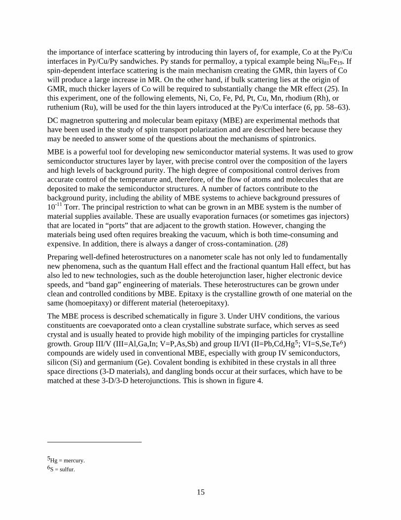
The MBE process is described schematically in figure 3. Under UHV conditions, the various constituents are coevaporated onto a clean crystalline substrate surface, which serves as seed crystal and is usually heated to provide high mobility of the impinging particles for crystalline growth. Group III/V (III=Al,Ga,In; V=P,As,Sb) and group II/VI (II=Pb,Cd,Hg5; VI=S,Se,Te6) compounds are widely used in conventional MBE, especially with group IV semiconductors, silicon (Si) and germanium (Ge). Covalent bonding is exhibited in these crystals in all three space directions (3-D materials), and dangling bonds occur at their surfaces, which have to be matched at these 3-D/3-D heterojunctions. This is shown in figure 4.
5Hg = mercury. 6S = sulfur.
15
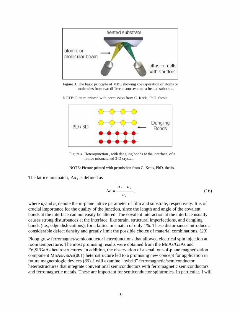
Figure 3. The basic principle of MBE showing coevaporation of atoms or
molecules from two different sources onto a heated substrate.
NOTE: Picture printed with permission from C. Kreis, PhD. thesis.
Figure 4. Heterojunction , with dangling bonds at the interface, of a lattice mismatched 3-D crystal.
NOTE: Picture printed with permission from C. Kreis, PhD. thesis.
The lattice mismatch, , is defined as aΔ
s
sf
a
aaa
−=Δ , (16)
where af and as denote the in-plane lattice parameter of film and substrate, respectively. It is of crucial importance for the quality of the junction, since the length and angle of the covalent bonds at the interface can not easily be altered. The covalent interaction at the interface usually causes strong disturbances at the interface, like strain, structural imperfections, and dangling bonds (i.e., edge dislocations), for a lattice mismatch of only 1%. These disturbances introduce a considerable defect density and greatly limit the possible choice of material combinations. (29)
Ploog grew ferromagnet/semiconductor heterojunctions that allowed electrical spin injection at room temperature. The most promising results were obtained from the MnAs/GaAs and Fe3Si/GaAs heterostructures. In addition, the observation of a small out-of-plane magnetization component MnAs/GaAs(001) heterostructure led to a promising new concept for application in future magnetologic devices (30). I will examine “hybrid” ferromagnetic/semiconductor heterostructures that integrate conventional semiconductors with ferromagnetic semiconductors and ferromagnetic metals. These are important for semiconductor spintronics. In particular, I will
16
look at hybrid heterostructures that combine conventional III-V and II-VI semiconductors with the ferromagnetic semiconductor (Ga,Mn)As and the ferromagnetic metal MnAs. I will focus on the characteristics of two novel classes of heterostructures:
1. (Ga,Mn)As/AlAs/MnAs magnetic tunnel junctions (MTJs) that provide an all electrical scheme for probing spin injection from metals into GaAs
2. n-ZnSe/(Ga,Mn)As heterojunction diodes that unexpectedly exhibit a magnetically driven photoconductivity
The injection of a spin-polarized current into semiconductors is an important requirement for semiconductor spintronic devices. Spin injection through a tunnel barrier can be probed by measuring the TMR in a semiconductor sandwiched between a double barrier MTJ with one tunnel barrier serving as the spin injector and the second as the spin detector. By varying the characteristics of the semiconductor (doping, thickness, etc.), one may probe a number of useful physical parameters, such as spin diffusion length that are directly related to semiconductor spintronics.
As a precursor to this experiment, spin-polarized tunneling in epitaxial single barrier MTJs comprised of a ferromagnetic metal, MnAs, and a ferromagnetic semiconductor, Ga1-xMnxAs, separated by a non-magnetic semiconductor, AlAs, have been studied. The hybrid MTJ provides a built-in control experiment since we can measure the TMR in both the paramagnetic and ferromagnetic states of Ga1-xMnxAs. An unusual feature of the hybrid metal/semiconductor MTJs—not the precursor experiment that has only one ferromagnetic substance—arises from the highly mismatched conductivities of the two ferromagnetic components: MnAs and Ga1-xMnxAs. Most studies of MTJs probe tunneling between materials with similar conductivity.
The MTJ samples have been fabricated by MBE on p+ – GaAs(001) substrates after the growth of a 40 nm-thick, p-GaAs buffer layer. The best configuration has been found to be Ga1-xMnxAs (x=0.03; thickness, 120 nm), GaAs (thickness, 1 nm), AlAs (thickness = 1,2,5 and 10 nm), GaAs (thickness, 1 nm), and MnAs (thickness, 45 nm) grown sequentially at 250 °C. Standard photolithography and wet-etching techniques have been used to define 300-µm diameter mesas (flat surfaces) for vertical transport measurements. Each mesa will be etched down into the p-GaAs region. Between the top MnAs layer and the back of the p-GaAs, a four-probe method will be used to measure the DC current-voltage characteristics of the mesas. These measurements are carried out in a continuous flow helium cryostat over a range of 4.2 K to 300 K with an in-plane magnetic field ranging up to 2 kG provided by an electromagnet. Additional transport measurements down to 330 mK are carried out in a He3 cryostat with a superconducting magnet. Lastly, magnetization measurements have been carried out on 10-mm2 pieces of the unpatterned wafer using a Quantum Device superconducting quantum interference magnetometer.
AlAsd
Quantitatively, the change in the tunnel resistance is given by
,12
MG
MG
P
PA
PPPP
RRR
TMR−
=−
= (17)
17
where RA and RP are the junction resistances with antiparallel and parallel moments, respectively. PG and PM are the spin polarizations of Ga1-xMnxAs and MnAs, respectively. From recent Andreev tunneling estimates of spin polarization, PG ≈85% and PM ≈40%, while the ideal TMR predicted by Julliere’s model is ≈100%. This suggests that the spin-dependent tunneling process observed in previous experiments of this kind is fairly efficient, ≈30% of the ideal TMR.
Detailed information about the AlAs barrier can be obtained through the analysis of conductance-voltage (G-V) curves (31).
Even though I will be carrying out an experiment from set eight in this project, I will describe the ninth set of experiments for completeness. This ninth set of experiments was carried out to measure the GMR in a perpendicular geometry. The perpendicular geometry yields larger effects, because there is no shunting of the current through normal metals; all of the current must undergo spin scattering at every interface to traverse the layered structure (32, 33). An immediate benefit of the perpendicular transport experiments is clarification of the physics of the transport process. In this geometry, a given electron can pass through many layers before “forgetting” its spin orientation (34).
With these experiments as a background, I will carry out experiments that combine the concepts and techniques developed in them to further investigate the concept of spin polarization transport in such materials as the Heusler alloys, and interpret and apply the results. As stated previously, a set eight type of experiment will be carried out.
It has been shown by Kammerer that the spin polarization of the Heusler alloy Co2MnSi (61%) at 10 K exceeds that of conventional transition metals, such as Ni80Fe20 (47%) and Co30Fe20 (37%) (35). Another result, due to Panchula, is that surface segregation of Mn and Sb reduces the spin polarization of the purported half-metal NiMnSb (36). For example, I will examine the effect of magnetic defects within the interior of a film, such as magnetic impurities in the nonmagnetic metal layer or inhomogeneity within the ferromagnetic layer, on the quantity and quality of spin scattering. I intend to focus on EPR and perturbation techniques and to examine the effect of domain wall movements on spin polarization dynamics, in addition to the set of experiments described above. I intend to use either an electromagnetic X-band (EMX) Series EPR spectrometer (produced by the Bruker BioSpin Corporation) at the U.S. Army Research Laboratory or the EPR spectrometer in the Chemistry Department at the University of Delaware. Since EPR can be used to make spin polarization measurements, I propose to make some of these measurements on selected Heusler alloys and decide if they can be used to make spintonic devices, such as those described in the Anticipated Results and Conclusions section of this article. Other experimental approaches that may be attempted in this study are injecting spin defects into a normal metal and observing the nuances using EPR and possibly other methods, such as Andreev reflection, an Aharonov-Bohm ring, a spin-polarized electron emitter, a compact analyzer of electron spin polarization, spin-polarized metastable-atom deexcitation spectroscopy (SPMDS), cyclotrons, a spin-guide source, a resonant interband tunneling device, point contact spectroscopy, a spin-polarized scanning tunneling microscope, and/or inhomogeneous doping. It won’t be possible to use all of these methods in this project, but a familiarity with each one will be obtained and examined to see if any, or all of them, can be useful to understanding the mechanisms of spintronics.
18
In particular, Andreev reflection is a scattering process, at an interface with a superconductor, responsible for a conversion between a dissipative quasi-particle current and a dissipationless supercurrent. This is a phase-coherent scattering process in which the reflected particle carries information about both the phase of the incident particle and the macroscopic phase of the superconductor. The advantage of this technique is the detection of polarization in a much wider range of materials than those which can be grown for detection in F/I/S or F/I/F tunnel junctions, where F stands for ferromagnetic, I stands for insulator, and S stands for semiconductor. (6)
A molecule in which the total spin of the electrons is one (S=1) is said to be in a triplet state. Two factors determine whether the ground state of a molecule is a singlet or triplet, namely, the orbital energies of the valence electrons and the strengths of the electrostatic exchange interactions between electrons of parallel spin. If two orbitals are sufficiently close together, the exchange energy predominates and the ground state of the molecule is a triplet. If there were only exchange and electrostatic interactions between electrons, the three sublevels of a triplet state would be exactly degenerate (split apart) and the EPR spectra would be very similar to those of radicals with spin of ½. The most important single fact about triplet states is that the magnetic dipole-dipole forces between the two unpaired electrons remove the degeneracy and lead to highly anisotropic spectra in most molecules. (37)
EPR can characterize the electron spin polarization of the excited quartet state of strongly coupled triplet-doublet spin systems. These systems (molecules) usually consist of a nitroxide radical or a paramagnetic metal bound to a chromophore, such as a porphyrin, phthalocyanine, or fullerene. They can be excited to produce an interacting triplet-doublet spin pair. The electron spin polarization is associated with electronic relaxation. These systems usually relax to the lowest triplet-quartet state by intersystem crossing from the trip doublet. When spin-orbit coupling is the main mechanism for this relaxation path, it leads to spin polarization of the trip quartet. Analytical expressions for this polarization have been derived using first- and second-order perturbation theory, which have, subsequently, been used to calculate powder spectra for typical sets of magnetic parameters.
Our system consists of a strongly exchange coupled triplet-doublet pair, which can be described by the spin Hamiltonian:
( ) ( ,312 ,
2,
2, TyTxTTzFTFFTT SSESSDSSJBgSgSH ΩΩΩ −+⎟
⎠⎞
⎜⎝⎛ −+−+= )rrrrr
β (18)
where the T refers to the triplet spin and orbitals involved, and F refers to the doublet spin and to the orbital carrying the unpaired electron. To simplify the expressions, we use the notation,
. The first part of the Hamiltonian is the Zeeman energy; the second part is the exchange interaction; and the third and fourth parts are the zero-field energy. J denotes the exchange interaction between the triplet and doublet, and and are their respective g tensors. D and E are the zero-field splitting parameters of the triplet spin state. Here the dipolar coupling between the triplet and doublet is much weaker than the zero-field splitting of the triplet and is ignored in the Hamiltonian, as are hyperfine interactions (38). To derive the expression for the zero-field energy (parts three and four), principal axes with principal values –X, –Y, and –Z were used to diagonalize the zero-field tensor, resulting in the expression
1=h
Tg Fg
. (19) 222zyx ZSYSXS −−−
19
However, since the trace of a Hamiltonian in a principal axis system is zero (X+Y+Z=0), the zero-field splitting can be rewritten in terms of just two independent constants, D and E, as shown in equation 18 (37).
The exchange coupling between the triplet and doublet is much larger than the difference in their Zeeman energies, ,BgJ βΔff and the Zeeman energy is much larger than the zero-field splitting, ED,ffω and
,ωββ h=≈ BgBg FT (20)
where and are the values of the respective triplet and doublet g tensors along the dof the magnetic field and gΔ is their difference.
Tg Fg irection
Therefore, the eigenfunctions of the Hamiltonian are separated into trip-doublet, D, and trip-quartet, Q, substrates using the following “ket” notation:
( ),23
121, 0αβ TTD −=+ + α+=+ TQ
23, , (21)
( ),23
121, 0βα TTD −=− − ( ),2
31
21, 0αβ TTQ +=+ + (22)
( ),23
121, 0βα TTQ +=− − (23)
.23, β−=− TQ (24)
where and are the triplet spin states, and±T 0T α and β are eigenstates of the doublet spin.
The spin polarization associated with these states depends on the pathway by which they are populated. If the two electrons of the triplet state have different exchange interactions with the third electron, the trip-doublet state (the two D kets in equations 21–24) acquires some singlet character from the sing-doublet state. Therefore, the transition from the sing-doublet to the trip-doublet is partially allowed and it is assumed that this is the dominant decay pathway for the sing-doublet. This assumption is supported by the observation that in systems such as porphyrin dimmers containing a paramagnetic center, this effect leads to intersystem crossing (ISC) rates, which are orders of magnitude faster than rates in corresponding diamagnetic complexes. It is possible, however, that in some systems spin-orbit coupling also plays a significant role in the decay of the excited sing-doublet. In these cases, an additional multiplet contribution to polarization of the trip-quartet state would be seen. Here we assume that this contribution is negligible and that following light excitation to the sing-doublet, the initial relaxation predominantly populates the trip-doublet sublevels. Ensuing doublet-quartet ISC, it then populates the quartet state (Q kets in equations 21–24). It is proposed that the main mechanism of this latter crossing process is spin-orbit coupling accompanied by fast internal conversion. “Internal conversion” is the effect caused by the spin-independent, intramolecular processes leading to relaxation between different orbital configurations. Because the time scales of these
20
two intramolecular processes are very different, the problem can be stated in terms of a static spin Hamiltonian, in which the spin-orbit coupling acts as a perturbation. In the molecular frame , the spin-orbit contribution has the form Ω
FFFTTTSO SLSLH ,,,, ΩΩΩΩ +=r rrr
λλ , (25)
where Tλ and Fλ are the spin-orbit coupling parameters and the vector operators, and TL ,Ω
rFL ,Ω
r,
describe the angular momentum for the orbitals in which the triplet and doublet spins reside. Rigorously speaking, this Hamiltonian is correct only for the one-center approximation of the spin-orbit interactions. However, for multicenter systems, one can use “effective” orbitals to represent the spin-orbit interaction in the form used in equation 25.
The basic postulates of this model can be summarized as follows:
• The trip-quartet state, Q kets in equations 21–24, is populated from the trip-doublet state, D kets in equations 21–24, due to intersystem crossing.
• The spin-spin interaction of the triplet and doublet parts of the system is fixed spatially with respect to one another, and, hence, does not vary. Therefore, the quartet spin polarization does not arise from level crossing (i.e., it is not due to variation of the exchange interaction) or from fluctuations of the dipolar interactions.
• The spin polarization is generally by internal processes rather than by intermolecular motion and interactions, because of the strong exchange coupling between the triplet and doublet spins.
• The degree of quartet-doublet mixing described by a static spin-orbit coupling Hamiltonian (equation 25) limits the rate of the doublet-quartet transitions.
The properties of most strongly exchange-coupled, triplet-doublet systems at low temperatures are characterized by these postulates. In addition, several approximations are introduced below in order to derive analytical expressions using perturbation theory.
Experimentally, liquid crystal solvents can be used to provide macroscopic ordering of EPR samples, and the ordering is maintained when the liquid crystal is frozen to the glass phase or crystalline solid phase in the magnetic field. The spectra of the samples thus prepared demonstrate the dependence of the net polarization and the θ2sin ( )3/1cos 2 −θ dependence of the multiplet contribution given by equation 26 for the traceless diagonal part of the quartet density matrix, QρΔ , describing the populations of the quartet state,
( ) ( ) ( ) 323
222
22
1 sin313/1cossin QzQQzQzQ SpSSpSp θθθρ +⎟
⎠⎞
⎜⎝⎛ −−+∝Δ , (26)
where θ is the angle between the z directions in molecular and laboratory coordinate systems. FTQ SSS += is the operator for the total spin of the quartet state, where T refers to the triplet
spin and orbitals involved and F refers to the doublet spin and to the orbital carrying the unpaired electron.
21
The parameters p1, p2, and p3 arise from the spin-orbit coupling induced quartet-doublet mixing and are given by
( )
21
14
pJJBg
p−+ΔΔ+
=β
, (27)
( )
22
22
2 6 −+
−+
ΔΔΔ+Δ
−= Tzpλ
(28)
and
,03 =p (29)
where indicates the exchange integral. 1J +Δ and −Δ are the energy differences between the trip-quartet and trip-doublet states, respectively, of different orbital configurations and can be written as
( ) ( ) 101 2JJQEDE Tz ++Δ=−=Δ+ (30)
and
( ) ( ) .2 101 JJDEQE Tz −−Δ=−=Δ− (31)
The spin-orbit coupling parameter is
.01 ,TzTTz LΩ= λλ (32)
The first-order operator, , corresponds to the net polarization, while the second-order
operator, , describes the multiplet component, and the third-order operator describes a combination of both the net and the multiplet components. The largest of the three amplitudes is p2 associated with the multiplet polarization, while p3 is zero to within our linear approximation. (38)
QzS2QzS
Since the net polarization is proportional to while the multiplet polarization follows θ2sin
⎟⎠⎞
⎜⎝⎛ −
31cos 2 θ , (33)
as seen above in the expression for QρΔ , only net polarization occurs when the molecular z axis is at the “magic angle.” (39).
The magic angle is 54.7° and use of it provides spectra with much better resolution. The magic angle is used primarily with nuclear magnetic resonance (NMR) in the magic angle spin NMR (MAS NMR) method, but is also employed with EPR. Under normal conditions, a solid sample would yield only an extremely broad featureless spectrum with a large contribution to the broadening arising from static dipolar interactions. Much of this initial broadening can be removed in solids by using high power proton (electrons for EPR) irradiation, often termed dipolar decoupling. But line widths of 5-10 KHz (NMR) or more can still remain. This broadening is due to chemical shift anisotropy. The observed broad envelope is a result of
22
contributions from the many individual chemical shifts of nuclei (electrons for EPR) in molecules oriented differently within the sample. The anisotropy can be effectively removed if the sample is spun rapidly at an angle of 54.7° with respect to the external magnetic field. (40)
On the other hand, for θ=0 (i.e., the z-direction parallel to the external magnetic field), no net polarization will be observed. This is because, with the molecule in this orientation, the spin states coupled by the spin-orbit interaction have the same projection along the field direction. Thus, the rate of decay of the two doublet sublevels with m=+1/2 and m=–1/2 are identical. However, there is net polarization in the quartet state for other molecular orientations relative to the magnetic field since the projection of the spin states differ and, therefore, the ISC rates from the two levels are also different. This effect also contributes to the concentration of the net polarization at the center of the spectrum, because the orientations for which the net polarization is strongest have their 2/32/1 ±↔±=m transitions at the center of the spectrum. (39)
The multiplet polarization is maximal when θ=0 (i.e. when the molecular symmetry axis is parallel to the external field); while the net contribution is maximal when the symmetry axis is perpendicular to the field. Hence, the net polarization is very weak and the multiplet polarization is very strong when the order parameter of the symmetry axis is Szz=0.7. Conversely, for negative valued parameters, Szz =–0.3, orientations with θ close to 90° are more likely and the net polarization is stronger. It was experimentally seen that the strength of the multiplet polarization for various valued parameters depends on the value of the zero-field splitting parameter E. When E=0, strong net polarization is observed for both positive and negative valued parameters, but the spectral positions of the maxima change. For positive valued parameters, features corresponding to the z component of the zero-field splitting tensor are dominant, while for negative valued parameters, the features from the x and y components of the tensor are most prominent. When the sample is rotated 90°, the distribution of orientations with respect to the field becomes broader and more isotropic. However, the relative intensity of the net and multiplet contributions is inverted when the sample is rotated, regardless of the sign of the parameter.
In the above discussion, the molecular axis about which effective spin-orbit coupling occurs was defined to be the molecular z axis. This direction may not necessarily be associated with the largest zero-field splitting, even though this direction will normally correspond to one of the principal zero-field splitting (ZFS) axes. Therefore, the z axis of the ZFS tensor, defined by the largest principal value, may be parallel to any one of the molecular axes x, y, or z. The scheme where the large principal value of the ZFS tensor corresponds to the molecular z axis was compared to a scheme where the axes correspond as follows:
(34) ,
,
molZFS yx →
(35) molZFS zy →
and
. (36) molZFS xz →
This change in ordering of the principal values of the ZFS tensor led to an inversion of the multiplet polarization, while the net polarization was unaffected by this change. This is because the sign of the multiplet contribution to the spectrum for a given orientation depends on both
23
⎟⎠⎞
⎜⎝⎛ −
31cos 2 θ and the sign of the zero-field splitting, while the sign of net polarization is
independent of these parameters. The latter is a result of the fact that the sign of the net polarization is determined by the sign of J, which is positive if the trip-quartet is lower in energy than the trip-doublet. Therefore, a variety of multiplet polarization patterns can be expected from molecules of different structure. On the other hand, net polarization is always predicted to be positive within a first-order perturbation treatment.
In summary, the first-order (linear) perturbation treatment leads to the following conclusions about the net and multiplet contributions to the spin polarization:
• The magnetic field dependence, spectral positions, and kinetic behavior of the two contributions are different and allow them to be separated.
• The ratio of their maximal intensities is proportional to the square of the spin-orbit coupling divided by the energy gap between the two lowest excited electronic configurations.
• The net polarization is predicted to be absorptive if the exchange interaction is positive.
• The orientation dependence of the multiplet and net contributions are opposite.
Second-order perturbation is mainly caused by two effects: off-diagonal terms of the spin Hamiltonian due to the spin orbit coupling and dipolar coupling of the triplet electrons. Both of these effects can modify the wave functions of the doublet and quartet states and introduce additional terms in the expressions for net polarization. Another consequence of second-order terms is that they cause a shift of the zero-field spin energy levels. Two limiting situations generate second-order (quadratic) terms:
1. When the exchange interaction of the higher excited states is negligible compared to the orbital energy gap, TzJ Δpp1
2. When the doublet-quartet splitting of higher orbital states is significant, 1JTz ≤Δ
The most important result of the second-order perturbation treatment is that the two polarization parameters dependent upon net polarization, p1 and p3 are both inversely proportional to the Zeeman energy,ω , and are, therefore, inversely proportional to the magnetic field strength:
Bg
Dpp eff
β∝∝ 31 , (37)
where is a zero-field splitting parameter (41) and B is the magnetic field intensity. There are crucial differences between the first- and second-order terms for net polarization if the spin-orbit interactions in different planes are comparable. In this case, the second-order terms mix doublet and quartet states of the same orbital configuration. Therefore, they are roughly proportional to the overall zero-field splitting parameter.
effD
Putting first- and second-order perturbation together, it is seen that the net polarization contributes to both the central peak and the outer wings of the spectrum. However, under some conditions, it can be considered that the central peak comes purely from net polarization, while the outer wings of the spectrum show only multiplet polarization. Spin polarization of the excited
24

doublet states can also occur. It can also happen that the net polarization of the quartet state can be generated by spin orbit coupling and can be observed while the excited doublet state remains unpolarized. (38)
The standard Monte Carlo method, sometimes called the method of statistical trials, has been used to study the dependence of MR and resistivity on temperature and field (42). The Monte Carlo method is based on random selections and was not practical before the advent of computers. This method can be illustrated by finding the area of a plane figure, S: Let the figure be completely within the unit square, choose at random N points in the square, and designate the number of points lying inside S by N’. Geometrically, the area of S is approximately equal to the ratio N’/N. The greater the N, the greater the accuracy of this estimate (43).
A Monte Carlo method developed for spin dynamics was applied to study spin-polarized transport properties of a 2-D electron gas in a semiconductor spin field-effect transistor (SFET) structure. The specific symmetry of spin-orbit terms (Rashba and Dresselhaus) leads to strong anisotropy of spin dynamics in the low field regime. Results derived from this study provided useful information to assist in optimization of the SFET performance (44). Monte Carlo simulations have also been performed to study the in-plane transport of spin-polarized electrons in III-V semiconductor quantum wells in the range 77-300 K (45). The Monte Carlo method has also been used to model spin injection through a Schottky barrier, where it was found that the injected current can maintain substantial spin polarization to a length scale of 1 µm at room temperature without external fields (46). The electron spin polarization was described by the spin density matrix, while the spatial dynamics of the electron was treated semi-classically. The coherent dynamics of the current spin polarization and spin dephasing were determined by the spin-orbit interaction. The electric field in the device was evaluated self-consistently with the charge distribution. The phonon and impurity electron momentum scattering mechanisms were incorporated in the simulation. The steady state spatial distribution of the current spin-polarization vector was simulated. The estimated value of the spin dephasing length at room temperature was of the order of 0.2 µm in the In0.52Al0.48As / In0.53Ga0.47As / In0.52Al0.48As FET structure with the quantum well grown in the (0, 0, 1) crystallographic direction (47).
7. Anticipated Results and Conclusions
The anticipated results are both of a theoretical nature and a practical nature. A robust spin injection into Si will be attempted. To date, control of spin in GaAs and in III-V ferromagnetic semiconductors has been achieved. We would like to extend this control to Si. This would add significantly to the current information technology. Important materials advances in improving the compatibility of Si/III-V structures suggest that this extension to Si might be able to be accomplished. Another result from this research might be that the effects of magnetic interfaces and material inhomogeneities on spin-polarized transport may be observed and understood. A comprehensive transport calculation in the created devices would provide valuable insights into both the spin polarization being measured and how it is reduced from the moment it was generated.
25
Another result will be accurate band-structure-derived calculations of spin relaxation times in both metals and semiconductors. Accurate calculations of the g factor, which has not been accomplished even for the elemental metals, may be carried out. A characterization of spin relaxation and decoherence (individual spin dephasing) of localized or confined electrons, when the hyperfine-interaction mechanism dominates, may be developed. Studying single-spin relaxation and decoherence may enhance the development of quantum computing.
Another result may be the realization of an all-optical NMR spectrometer. To accomplish this, periodically optically excited electron spins will play the role of the resonant radio waves. The operation of a spin laser has been demonstrated. The laser previously demonstrated was a vertical-cavity surface-emitting laser (VCSEL). It was optically pumped in the gain medium, which was two quantum wells with 50% spin-polarized electrons. The results of this current project may be able to be used in the development of such an all-optical NMR instrument.
Major results of this research should be in the area of spintronic devices. This area will be developed because of the concept that the flow of spin-polarized carriers, rather than applied magnetic field, can be used to manipulate magnetization of ferromagnetic materials. Coherent microwave oscillations in nanomagnets form a basis for these devices. These oscillations are the result of both the reversal of magnetization and the driving of a spin-polarized current. Results about spin-transfer torque should be forthcoming. It has already been realized in geometries that possess a very large current density. It is expected that much smaller switching currents will be required to demonstrate spin-transfer torque (together with other cooperative phenomena) in ferromagnetic semiconductors. This effect will be experimentally tested. We will show that reversal of magnetization in (In,Mn)As can be manipulated by modifying the carrier density using a gate voltage in a field-effect transistor structure. (7, pp. 385–6)
Another spintronic device is the spin valve. It is a GMR device, which consists of two ferromagnetic layers sandwiching a thin nonmagnetic metal layer with one of the magnetic layers being “pinned”, i.e., the direction of the magnetization of the layer is relatively insensitive to moderate magnetic fields. The other magnetic film is called the “free” layer and the direction of its magnetization can be changed by applying relatively small magnetic fields. In this device, the resistance typically rises 5% to 10% as the orientation of the magnetization of the ferromagnetic layers changes from parallel to antiparallel. Pinning in the “pinned” layer is achieved by using an antiferromagnetic layer in contact with it. NiMnSb is a candidate material for spin valves. Its coercive field is of great importance, since it defines the operating magnetic field range of active devices. Thus, it is desirable that the grown films possess a low Hc, coercive field.
Yet another spintronic device is the MTJ. It also consists of two ferromagnetic layers sandwiching, this time, a very thin insulating layer, such as Al2O3. The tunneling resistance is modulated by a magnetic field in the same way as the resistance of a spin valve and changes, usually 20% to 40%. It requires saturation magnetic fields equal or less than those required for spin valves.
The spin transistor is a theoretical device that has initiated a vigorous search for electrical spin injection from ferromagnetic films into semiconductors. It consists of two ferromagnetic layers sandwiching a narrow semiconductor channel. In this device, spin-aligned electrons are injected from one of the magnetic films, called the emitter, into the semiconductor channel. After traveling through this channel, they are detected by the other magnetic film, called the collector.
26
A gate electrode over the semiconductor channel creates a field that causes a magnetic interaction, making the spins precess. When the gate voltage is off, the aligned spins can propagate from the emitter to the collector through the semiconductor channel. When the gate voltage is on, the spins precess and current passes through the semiconductor channel only if the spins are aligned with the magnetization of the collector (2). Three important examples of the spin transistor are the Datta-Das SFET, the magnetic bipolar transistor, and the hot-electron spin transistor (7). Datta and Das have proposed a spin transistor that is a hybrid semiconductor device employing a direct electrical spin injection from a ferromagnetic substance into a nonmagnetic superconductor (5). The spin injection and spin detection are carried out by a ferromagnetic source and drain, and by spin precession about the built-in structure inversion asymmetry (Bychkov-Rashba) field in the asymmetric, quasi-one-dimensional channel of the ordinary field-effect transistor. Here the precession vector is
( ) ( )nkk BRrr rr
×=Ω α2 , (38)
where kr
is the wave vector for a Bloch state propagating in the plane, nr is the confinement unit vector of the quantum well, and BRα is a parameter depending on spin-orbit coupling and the asymmetry of the confining electrostatic potentials arising from the growth process of the heterostructure. The attractive feature of the Datta-Das SFET is that spin-dependent device operation is not controlled by external magnetic fields, but by gate bias, which controls the spin precession rate.
The magnetic bipolar transistor (MBT) is a bipolar transistor with spin-split carrier bands and, in general, an injected spin source. A related device structure, a spin-polarized injection current emitter (SPICE), has semiconductors with no equilibrium spin, while the spin source is provided by a ferromagnetic spin injector attached to the emitter. Another ferromagnetic metal, a spin detector, is attached to the base/collector junction to modulate the current flow. In both configurations, the aim is to control current amplification by spin and magnetic field.
The current amplification (gain),
B
C
II
=β , (39)
is typically approximately 100 in practical transistors. This ratio depends on many factors, such as the doping densities, carrier lifetimes, diffusion coefficients, and structure geometry. In an MBT, β also depends on the spin splitting, ςq2 , and the non-equilibrium polarization, EPδ . This additional dependence of β in an MBT is called magnetoamplification. An important prediction is that non-equilibrium spin can be injected at low bias all the way from the emitter, through the base, to the collector in order to make an effective control of β by EPδ possible.
The MBT is, in effect, a magnetic heterostructure transistor, since its functionality depends on tenability of the band structure of the emitter, base, or collector. The advantage of the MBT is that the band structure can be tuned during the device operation by magnetic field or spin injection signals rather than being built in, but can be tuned during the device operation by magnetic field or spin injection signals.
27
The MBT has an equilibrium and non-equilibrium (magnetization) in the emitter, base, or collector. The two main physical phenomena associated with the low-injection theory of spin-polarized transport through MBTs are electrical spin injection and spin control of current amplification (magnetoamplification). A source spin can be injected from the emitter to the collector. If the base of an MBT has an equilibrium magnetization, the spin can be injected from the base to the collector by intrinsic spin injection. The resulting spin accumulation in the collector is proportional to
( )TkqV Bbe /exp , (40)
where q is the proton charge, is the bias in the emitter-base junction, and is the thermal energy. To control the electrical current through MBTs, both the equilibrium and the non-equilibrium spin can be used. The equilibrium spin controls the magnitude of the equilibrium electron and hole densities, thereby controlling the currents. The current amplification is increased (decreased) by increasing the equilibrium spin polarization of the base (emitter). A spin-valve effect can arise if there is a non-equilibrium spin in the emitter, and the base or the emitter has an equilibrium spin. This spin-valve effect can lead to a giant magnetoamplification effect, where the current amplifications for the parallel and antiparallel orientations of the equilibrium and non-equilibrium spins differ significantly. (8, p. 115314–1)
beV TkB
The third type of spin transistor, the hot-electron spin transistor, relies on transport of hot, or non-thermalized, carriers. They have the potential of serving several different purposes. First, they could be used as a diagnostic tool to characterize spin- and energy-dependent interfacial properties, scattering processes, and electronic structure relevant to spin devices. Secondly, they are of interest for their ability to sense magnetic fields, their possible memory applications, and their potential as a source of ballistic hot-electron spin injection. Two proposed types of hot-electron spin transistors are the spin-valve transistor and the magnetic tunneling transistor.
The spin-valve, or Monsma transistor, integrates metallic ferromagnets and semiconductors. It is a three-terminal structure consisting of a metallic base, B, made of a ferromagnetic multilayer in a current perpendicular to the plane (CPP) GMR geometry surrounded by a silicon emitter, E, and collector, C, with two Schottky contacts formed at E/B and B/C interfaces. This three-terminal structure, which has a small current gain (a small change in the base current leads to a large change in the collector current) of approximately 2, is in contrast to the two-terminal structure of a conventional semiconductor transistor that has a large current gain. Forward bias, , controls the emitter current, , of spin-unpolarized electrons, which are injected into a base region as hot carriers. The scattering processes in the base, together with the reverse bias, , influence how many of the injected electrons can overcome the B/C Schottky barrier and contribute to the collector current, . The magnetoresistive response is usually expressed using magnetocurrent (MC), defined as the change in collector current normalized to the minimum value
EBV EI
BCV
CI
( )
↑↓
↑↓↑↑ −=C
CC
III
MC , (41)
28
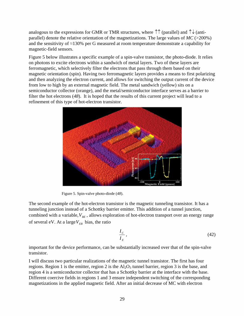
analogous to the expressions for GMR or TMR structures, where (parallel) and ↑↓ (anti-parallel) denote the relative orientation of the magnetizations. The large values of MC (>200%) and the sensitivity of ≈130% per G measured at room temperature demonstrate a capability for magnetic-field sensors.
↑↑
Figure 5 below illustrates a specific example of a spin-valve transistor, the photo-diode. It relies on photons to excite electrons within a sandwich of metal layers. Two of these layers are ferromagnetic, which selectively filter the electrons that pass through them based on their magnetic orientation (spin). Having two ferromagnetic layers provides a means to first polarizing and then analyzing the electron current, and allows for switching the output current of the device from low to high by an external magnetic field. The metal sandwich (yellow) sits on a semiconductor collector (orange), and the metal/semiconductor interface serves as a barrier to filter the hot electrons (48). It is hoped that the results of this current project will lead to a refinement of this type of hot-electron transistor.
Figure 5. Spin-valve photo-diode (48).
The second example of the hot-electron transistor is the magnetic tunneling transistor. It has a tunneling junction instead of a Schottky barrier emitter. This addition of a tunnel junction, combined with a variable, , allows exploration of hot-electron transport over an energy range of several eV. At a large bias, the ratio
BEV
EBV
E
C
II
, (42)
important for the device performance, can be substantially increased over that of the spin-valve transistor.
I will discuss two particular realizations of the magnetic tunnel transistor. The first has four regions. Region 1 is the emitter, region 2 is the Al2O3 tunnel barrier, region 3 is the base, and region 4 is a semiconductor collector that has a Schottky barrier at the interface with the base. Different coercive fields in regions 1 and 3 ensure independent switching of the corresponding magnetizations in the applied magnetic field. After an initial decrease of MC with electron
29
energy, at VEB ≈ 0.3 V larger than the base/collector Schottky barrier, there is an onset of hot-electron transport into L valleys accompanied by an increase in MC. A large MC alone, measured in various hot-electron spin transistors, is not sufficient to demonstrate spin injection in a semiconductor collector. For conclusive evidence spin detection in a collector region is needed. This was first achieved using optical detection with a spin LED structure added to the collector. Measurements at T=1.4 K and B=2.5 T, after a background subtraction, showed majority spin injection with Pcirc ≈ 10%.
The second realization of the magnetic tunnel transistor is more similar to the original spin-valve transistor. In this case, the emitter was nonmagnetic (Cu) while the base was a magnetic multilayer (F1/N/F2). The resulting strong spin-filtering effect can be inferred from the transmitted hot carriers with a spin-dependent exponential decay within the Fi layer, where i=1,2. The resulting magnetocurrent can be expressed as
( ) ,12
21
21
NN
NN
PPPP
MC−
= (43)
which is analogous to TMR using Julliere’s model, but with the redefined definition of spin polarization. At VEB ≈ 0.8 V and at T=77 K, the measured MC exceeds 3400%, while, using the last equation, the polarization of the transmitted electrons can be estimated to exceed 90%, even with a ferromagnet only ≈ 3 nm thick. Increased spin injection, even at room temperatures, are expected to result from future studies of hot-electron spin transistors. Other semiconductor collectors will probably be used in future studies, as well. It would be particularly desirable to demonstrate hot-electron spin injection in Si and to facilitate an integration with the complementary metal-oxide semiconductor (CMOS) technology. (7, pp. 380–384)
Furthermore, it was demonstrated by Hong and Wu that the spin dependent collector current in a hot-electron spin-valve transistor can be manipulated through changing Schottky barrier characters such as height and width (49). This result will be useful for device design.
Also, electrical spin injection has been demonstrated from ferromagnetic thin films into a 2-D electron gas semiconductor system. However, the spin injection was inefficient. This inefficiency is perhaps mainly due to the conductivity mismatch of the ferromagnetic metal and the semiconductor, and secondly due to the low spin polarization of the Py, which was only 35%. It has been proposed that this conductivity mismatch can be improved with the introduction of a tunnel barrier between the ferromagnetic layer and the semiconductor. On the other hand, the spin polarization of the emitter contact can be improved using ferromagnetic materials which are called half-metals and are expected to present 100% spin polarization. (2)
Another possible result could be the world’s first plastic magnet suitable for use as a storage medium in consumer products. Spintronics could be the idea behind the development of such a material, which could eventually replace more costly metals in computer hard drives. A new magnetic polymer, called PANiCNQ, has already been developed for this purpose by the University of Durham in the United Kingdom. They have discovered a method to induce magnetism in their material, showing some promise for its future use as a magnetic recording medium. Like most plastics, this material is cheap to synthesize, easy to process, and can be molded into any desired shape. It could be used in such products as portable music or video players, hand-held computers, or recording media for digital cameras. These devices don’t require high recording densities. Prior magnetic plastics have either worked only in oxygen-free
30
environments at temperatures too low for practical use or offered very weak magnetism at higher temperatures. The Durham researchers made their magnetic compound by combining emeraldine base polyaniline (PANi), a conductive plastic, and tetracyanoquinodimethane (TCNQ), a polymer. Over a three-month period, they detected an increase in the material’s magnetism to the point that a magnet would pick up powdered PANiCNQ. Then, they found that they could change the proportions of PANi and TCNQ to alter the compound’s magnetism as needed. The new compound was neither highly nor uniformly magnetic, but they contend that these problems can be solved. In conventional magnetism, a material’s electron spins line up to exert a force on some types of metals. The Durham team paralleled this mechanism by creating an alignment of free radicals. The usefulness of this new compound for hard drives is questionable since they are already one of the cheapest forms of storage, but plastics are inexpensive to mass produce and eventually might be useful in some sort of storage medium. It may be possible to make the technique yield more PANiCNQ and to make the material more magnetic. It will probably take between 5 and 10 years to make the compound available for commercial use. (50)
Further applications of this project may occur in the field of quantum computing. Quantum computing offers the potential for dealing with certain intractable problems of conventional digital computing. A quantum computer would contain thousands of devices and would probably be built with solid-state technology. The challenge for solid-state quantum computing is to find a way to use devices without precise knowledge of their physical characteristics. Quantum computing is implemented with “qubits,” physical systems that are in either of two distinguishable quantum states that represent information: one state is zero and the other a one. The power in this system comes from the processing of many variables simultaneously by using a superposition of quantum states. Wave functions-solutions of the quantum Schrödinger equation for qubits-define the states in the case of quantum computing. A qubit’s states can be identified with zero and one, and their wave functions written as 0φ and 1φ . A qubit can also be represented by the superposition of the two states:
10 φφψ ba += , (44)
where a and b are complex numbers satisfying . This superposition principle offers a means of carrying a much larger amount of information. Another quantum phenomenon, called entanglement, ties the wave functions of the qubits in a register together in a way that makes it possible to affect each member of the superposition, creating great power on quantum computing.
122 =+ ba
Most of the successful experimental demonstrations of qubits have used superconducting devices. An experiment using a superconducting Coulomb box as the qubit provides an example. A Coulomb box is a structure with a capacitance so small that the energy needed to add a single electron to it is the dominant energy in the operation of a circuit. The box in this experiment is called a “Cooper-pair box,” because the energy of the electrons can be lowered by the formation of Cooper pairs. The box can exchange charge with a reservoir through Josephson junctions. Solid-state technology produces devices on a planar surface. Neighboring qubits on a surface might interact with one another through overlapping wave functions, or through a capacitive link, used with superconducting qubits. However, it is difficult to see how to provide the long point-to-point connections that quantum computing requires.
31
Decoherence is another quantum phenomenon that must be addressed. It is an unwanted interaction of quantum information with extraneous entities that destroy the information that the system is processing. An error-correction method that compares redundant qubits at each step has been proposed to combat decoherence. Forming accurate superpositions requires specifying separate timing sequences for each qubit and tailoring interaction times to each pair. The quantum computing alternative can be described as redundancy in quantum error correction and may be an anticipated result of this spintronics project. (50, pp. 65–69)
The technique for manipulating and measuring DWs that will be investigated in this project may be useful in ferromagnetic semiconductor devices for magnetic logic and memory. The technique may also provide a new path for measuring quantum signatures of DW motion at low temperatures, where macroscopic quantum tunneling should be seen. (16)
Another possible outcome of this research could be a liquid state NMR computer, which is based on nuclear spin states of molecules in solution. A five-qubit order finding algorithm has been demonstrated for this concept. One problem associated with the NMR computer is scalability, since the signal-to-noise ratio decreases exponentially as the size of the molecule increases. (5)
32
References
1. Kittel, C. Quantum Theory of Solids; John Wiley & Sons, Inc.: New York-London, 1963, p 237–248.
2. Gardelis, S.; Androulakis, J.; Migiakis, P.; Giapintzakis, J. Recent Advances in Spintronics. Half-Metal Ferromagnets: Their Role in Spintronics; Materials Science Forum, Vol. 455-456; Trans Tech Publications: Switzerland, 2004; pp 137–142.
3. Samarth, N. An Introduction to Semiconductor Spintronics. Solid State Physics 2004, 58.
4. Schmidt, G.; Gould, C.; Molenkamp, L.W. Spintronics in Semiconductor Nanostructures. Physica E 2004, 25, (2-3), 150–159.
5. Govind; Joshi, S.K. Spintronics and Quantum Computation. Indian J. of Physics 2004, 78A (3), 299–308.
6. Prinz, G. Physics Today, April 1995, 60.
7. Zutic, I. et al. Spintronics: Fundamentals and Applications. Reviews of Modern Physics April 2004, 76, 324.
8. Fabian, J.; Zutic, I. Spin-Polarized Current Amplification and Spin Injection in Magnetic Bipolar Transition. Physical Review B, The American Physical Society, 2004, 69, 115314-1 to 115314-13.
9. McGraw-Hill Encyclopedia of Physics, Parker, S.P., editor-in-chief; McGraw Hill Book Company: New York, 1983, p 766–7.
10. Palmstrom, C. Epitaxial Heusler Alloys: New Materials for Semiconductor Spintronics. Materials Research Society Bull. Oct 2003, 725–728.
11. Kubota, H.; Nakata, J.; Oogane, M. et al. Large Magnetoresistance In Magnetic Tunnel Junctions Using C0-Mn-Al Full Heusler Alloys, Japanese J. of Applied Physics, The Japanese Society of Applied Physics, 2004, 43 (7B), L 984–L 986.
12. Spin Dynamics in Confined Magnetic Structures. Hillebrands and Ounadjela, Eds.; Topics in Applied Physics 2002, 83.
13. Moodera; M. Spin Polarized Tunneling in Ferromagnetic Junctions. J. of Magnetism and Magnetic Materials 1999, 261–270.
14. Universita degli Studi di Milano Web site. www.mi.infm.it/manini/berryphase.html (accessed July 11, 2005).
15. Strand, D.J. Barkhausen Noise Analysis and Ferromagnetic Materials; MTL TR 89 108, U.S. Army Materials Technology Laboratory: Watertown, MA, December 1989, pp 1–3.
16. Tang, Nature, 2 Sept 2004, 431, 52–56.
33
17. Esaki, L.; Stiles, P.J.; von Molnar, S. Physical Review Letters 1967, 19, 852 and Thompson, W.A.; Holtzberg, F.; McGuire, T.R. Physical Review Letters 1971, 26, 1308.
18. Meservey, P.M.; Tedrow, P.M.; Fulde, P. Physical Review Letters 1970, 25, 1270.
19. Julliere, M. Physics Review Letters 1975, 54A, 225.
20. Feher, G.; Kip, A.F. Physical Review Letters 1955, 98, 337 and Dyson, F.J. Physical Review Letters 1955, 98, 349.
21. Johnson, M.; Silsbee, R.H. Physical Review Letters 1985, 55, 1790.
22. Baibich, M.N.; Broto, J.M.; Fert, A.; Nguyen va Dau, F.; Petroff, F.; Etienne, P.; Creuzet, G.; Friedrich, A.; Chazeles, J. Physical Review Letters 1988, 61, 2472.
23. Schad, R.; Potter, C.D.; Belien, P.; Verbanck, G.; Moshchalkov, V.V.; Bruynseraede, Applied Physics Letters 1994, 64, 3500.
24. Zhang, S. et al. Physical Review B 1992, 45, 8689.
25. Parkin, S.S.P. Origin of Enhanced Magnetoresistance of Magnetic Multilayers: Spin-Dependent Scattering from Magnetic Interface States. Physical Review Letters 6 Sept 1993, 71 (10), 1641.
26. McGraw-Hill Dictionary of Materials Science, Licker, M.D., publisher; The McGraw-Hill Companies, Inc.: New York, 2003.
27. McGraw-Hill Dictionary of Scientific and Technical Terms, Fifth Ed.; Parker, S.P., editor-in-chief; McGraw-Hill, Inc.: New York, 1994.
28. Campion, R. MBE Lays Foundations for Spintronics. Physics World Oct 2004, 17 (10), A19.
29. Molecular Beam Epitaxy (MBE) Web site. www.ieap (accessed April 14, 2005).
30. Ploog, K.H. Epitaxial Ferromagnet-Semiconductor Heterostructures for Electrical Spin Injection. J. of Crystal Growth 1 Aug 2004, 268, Issues 3–4, 329–335.
31. Samarth, N.; Chun, S.H.; Ku, K.C. et al. Hybrid Ferromagnetic/Semiconductor Heterostructures for Spintronics. Solid State Communications 2003, 127, 173–179.
32. Pratt Jr., W.A.; Lee, S.F.; Slaughter, J.M.; Loloee, R.; Schroder, P.A.; Bass, J. Physical Review Letters 1991, 66, 3060.
33. Gijs, M.A.M.; Lenczowski, S.K.J.; Giesbers, J.B. Physical Review Letters 1993, 70, 3343.
34. Valet, T.; Fert, A. Physical Review B 1993, 48, 7099.
35. Kammerer, S. et al. Co2MnSi Heusler Alloy as Magnetic Electrodes in Magnetic Tunnel Junctions. Applied Physics Letters 5 July 2004, 85 (1), 79 and 81.
36. Panchula, Alex F. et al. Spin Polarization and Magnetotransport of Mn-Sb Alloys in Magnetic Tunnel Junctions. Applied Physics Letters 1 Sept 2003, 83 (9), 1812.
34
37. Carrington, A.; McLachlan, A.D. Introduction to Magnetic Resonance; Halsted Press, John Wiley & Sons, Inc.: New York, 1979.
38. Kandrashkin, Y.; Van der Est, A. Electron Spin Polarization of the Excited Quartet State of Strongly Coupled Triplet-Doublet Spin Systems. J. of Chemical Physics 8 March 2004, 120 (10), 4797–9.
39. Kandrashkin, Y.; Van Der Est, A. Light-Induced Electron Spin Polarization In Rigidly Linked, Strongly Coupled Triplet-Doublet Spin Pairs. Chemical Physics Letters 2003, 379, 574–580.
40. NMR Spectroscopy: New Methods and Applications, Levy, G.C., Ed., ACS Symposium Series 191; American Chemical Society: Washington, D.C., 1982.
41. Gade, S.; Strand, D.; Knispel, R. A Method for Extracting the Zero-Field Splitting Tensor from EPR Rotation Data for S=1 Paramagnetic Centers. J. of Magnetic Resonance 1985, 64, 395–7.
42. Huang, Z.; Chen, Z.; Peng, K. et al. Monte Carlo Simulation of Tunneling Magnetoresistance in Nanostructured Materials. Physical Review B, The American Physical Society, 2004, 69, pp. 094420-1 to 7.
43. Sobol, I.M. The Monte Carlo Method; The University of Chicago Press: Chicago, Illinois, 1974, p 2–3.
44. Saikin, S.; Shen, M.; Cheng, M.C. Study of Spin-Polarized Transport Properties for Spin-FET Design Optimization. IEEE Transactions on Nanotechnology March 2004, 3 (1), 173–179.
45. Shen, M.; Saiken, S.; Cheng, M.C. et al. Monte Carlo Simulation of Spin-Polarized Transport, Lecture Notes in Computer Science, 2668, Springer-Verlag: Berlin, 2003, pp 881–891.
46. Shen, M.; Saiken, S.; Cheng, M.C. Monte Carlo Modeling of Spin Injection Through a Schottky Barrier and Spin Transport in a Semiconductor Quantum Well. J. of Applied Physics, The American Institute of Physics, 15 Oct 2004, 96 (8), 4319–4325.
47. Shen, M.; Saikin, S.; Cheng, M.C. et al. Monte Carlo Modeling of Spin FETs Controlled by Spin-Orbit Interaction. Mathematics and Computers in Simulation 2004, 65, 351–363.
48. The Narayanamurti Group Web page. www.deas.harvard.edu/venky (accessed April 17, 2005).
49. Hong, J.; Wu, R.Q. Hot Electron Spin Polarization and Schottky Barrier In Spin-Valve Transistor. J. of Applied Physics, The American Institute of Physics, 15 April 2004, 95 (8), 4240–4244.
50. Paulson, L.D. Computer, IEEE Computer Society: New York, NY, Jan 2005, 38 (1), 25.
35
Acronyms
2-D two-dimensional
3-D three-dimensional
AC alternating current
AHE anomalous Hall effect
AMR anisotropic magnetoresistance
BNA Barkhausen Noise Analysis
CCMS Center for Computational Materials Science
CMOS complementary metal-oxide semiconductor
CPP current perpendicular to the plane
DC direct current
DWR domain wall resistance
DWs domain walls
EBS exchange-biased sandwiches
EDXD energy-dispersive X-ray diffraction
EMX electromagnetic X-band
EPR electron paramagnetic resonance spectroscopy
F ferromagnetic
fcc face-centered-cubic
FET field-effect transistor
FM ferromagnetic
GMR giant magnetoresistance
G-V conductance-voltage
I insulator
ISC intersystem crossing
JMR junction magnetoresistance
LED light emitting diode
MAS NMR magic angle spin nuclear magnetic resonance
MBE molecular beam epitaxy
MBT magnetic bipolar transistor
36
MC magnetocurrent
MR magnetoresistance
MRAM magnetic random access memory
MTJ magnetic tunnel junction
NMR nuclear magnetic resonance
PANi polyaniline
PLD pulsed laser deposition
Py permalloy
S semiconductor
SFET spin field-effect transistor
SPICE spin-polarized injection current emitter
spin electronics spintronics
SPMDS spin polarization, spin-polarized metastable-atom deexcitation spectroscopy
SQUID superconducting quantum interference device
TCNQ tetracyanoquinodimethane
TMR tunnel magnetoresistance
UHV ultra-high vacuum
VCSEL vertical-cavity surface-emitting laser
XPS X-ray Photoelectron Spectroscopy
ZFS zero-field splitting
37
Bibliography
Battle et al. J. of Applied Physics 2002, 91, 10163–10168.
Bobo et al. J. of Applied Physics 1998, 83, 6685–6687.
Caballero et al. J. of Vacuum. Science Technology A 1998, 16, 1801–1805.
Comstock. J. of Materials Science: Materials in Electronics 2002, 13, 509–523.
Koller et al. J. of Applied Physics 2003, 93, 8549–8551.
Landry et al. Applied Physics Letters 2001, 78, 501–503.
Mitsuzuka et al. J. of Applied Physics 1999, 85, 5807–5809.
Moodera and Mathon. J. of Magnetism and Magnetic Materials 1999, 200, 248–273.
Moodera et al. Applied Physics Letters 1997, 70, 3050–3052.
Prinz. Physics Today, April 1995, pp 58–63.
Ritchie et al. J. of Magnetism and Magnetic Materials 2002, 247, 187–197.
Zhang. Physical Review Letters 1999, 83, 640–643.
Zhu and Zheng. Spin Dynamics in Confined Magnetic Structures. Topics in Applied Physics 2002, 83, 289–326.
38
Distribution List
NO. OF COPIES ORGANIZATION
1* DEFENSE TECHNICAL INFO CTR ATTN DTIC OA MS CORA SANTOS 8725 JOHN J KINGMAN RD STE 0944 FT BELVOIR VA 22060-6218 *pdf only 1 HQDA DAMO FDT 400 ARMY PENTAGON WASHINGTON DC 20301-0460 1 COMMANDING GENERAL US ARMY MATERIEL CMD AMSRD SS T 6000 6TH STREET STE 100
FT BELVOIR VA 22060-5608
1 US ARMY RESEARCH LAB ATTN IMNE ALC IMS MAIL & RECORDS MGMT ADELPHI MD 20783-1197 2 US ARMY RESEARCH LAB AMSRD ARL CI OK TL TECHL LIB 2800 POWDER MILL ROAD ADELPHI MD 20783-1197 ABERDEEN PROVING GROUND 2 AMSRD CI OK TP TECHL LIB 35 + US ARL 3 CDs ATTN AMSRD ARL WM MC D STRAND
NO. OF COPIES ORGANIZATION
1 DIRECTOR DA OASARDA SARD SO 103 ARMY PENTAGON WASHINGTON DC 20301-0103 1 COMMANDER US ARMY MATERIEL CMD AMXMI INT 9301 CHAPEK RD FT BELVOIR VA 22060-5527 4 COMMANDER US ARMY ARDEC AMSTA AR CCF D J GEHBAUER PICATINNY ARSENAL NJ 07806-5000 5 COMMANDER US ARMY ARDEC AMSRD AAR EM S MUSALLI BLDG 65S AMSRD AAR EBM R CARR BLDG 1 AMSRD AAR AEM L M LUCIANO E LOGSDEN T LOUZEIRO BLDG 65 PICATINNY ARSENAL NJ 07806-5000 1 COMMANDER US ARMY ARDEC AMSRD AAR AEM D J LUTZ BLDG 354 PICATINNY ARSENAL NJ 07806-5000 1 COMMANDER US ARMY ARDEC SFAE AMO MAS SETI C LIVECCHIA BLDG 354S PICATINNY ARSENAL NJ 07806-5000
39
NO. OF COPIES ORGANIZATION
1 COMMANDER US ARMY ARDEC AMSRD AAR EMO F PICATINNY ARSENAL NJ 07806-5000 1 COMMANDER US ARMY ARDEC SFAE AMO CAS C PATEL BLDG 171N PICATINNY ARSENAL NJ 07806-5000 1 COMMANDER US ARMY ARDEC AMSRD AAR AEM C D DEMELLA BLDG 61S PICATINNY ARSENAL NJ 07806-5000 2 COMMANDER US ARMY ARDEC AMSRD AAR ATD B MACHAK BLDG 1 AMSRD AAR AEW A(D) M CHEIFA BLDG 61N PICATINNY ARSENAL NJ 07806-5000 1 COMMANDER US ARMY ARDEC AMSTA AR FSP A P KISATSKY PICATINNY ARSENAL NJ 07806-5000 2 COMMANDER US ARMY ARDEC AMSRD AAR AEM L S CHICO BLDG 65 PICATINNY ARSENAL NJ 07806-5000 1 COMMANDER US ARMY ARDEC SFAE AMO MAS LC D RIGOGLIOSO BLDG 354 PICATINNY ARSENAL NJ 07806-5000
NO. OF COPIES ORGANIZATION
6 COMMANDER US ARMY ARDEC AMSRD AAR AEM L P DONADIA F DONLON P VALENTI S PATEL R SAYER BLDG 65S SFAE AMO MAS LC F CHANG BLDG 354 PICATINNY ARSENAL NJ 07806-5000 2 COMMANDER US ARMY ARDEC AMSRD AAR AEM I D CONWAY AMSRD AAR AEW E(D) R SCHLENNER BLDG 65N PICATINNY ARSENAL NJ 07806-5000 1 COMMANDER US ARMY ARDEC AMSRD AAR AEE E D YEE BLDG 19 PICATINNY ARSENAL NJ 07806-5000 6 PM SADARM SFAE GCSS SD COL B ELLIS M DEVINE R KOWALSKI W DEMASSI J PRITCHARD S HROWNAK PICATINNY ARSENAL NJ 07806-5000 2 PEO FIELD ARTILLERY SYS SFAE FAS PM H GOLDMAN T MCWILLIAMS PICATINNY ARSENAL NJ 07806-5000
40
NO. OF COPIES ORGANIZATION
11 PM TMAS SFAE GCSS TMA R MORRIS C KIMKER D GUZOWICZ E KOPACZ R ROESER R DARCY R MCDONALDS L D ULISSE C ROLLER J MCGREEN B PATTER PICATINNY ARSENAL NJ 07806-5000 1 COMMANDER US ARMY ARDEC AMSTA AR WEA J BRESCIA PICATINNY ARSENAL NJ 07806-5000 1 COMMANDER US ARMY TACOM PM ABRAMS SFAE ASM AB 6501 ELEVEN MILE RD WARREN MI 48397-5000 1 COMMANDER US ARMY TACOM AMSTA SF WARREN MI 48397-5000 3 COMMANDER US ARMY TACOM PM TACTICAL VEHICLES SFAE TVL SFAE TVM SFAE TVH 6501 ELEVEN MILE RD WARREN MI 48397-5000 1 COMMANDER US ARMY TACOM PM BFVS SFAE ASM BV 6501 ELEVEN MILE RD WARREN MI 48397-5000
NO. OF COPIES ORGANIZATION
1 COMMANDER US ARMY TACOM PM AFAS SFAE ASM AF 6501 ELEVEN MILE RD WARREN MI 48397-5000 1 COMMANDER US ARMY TACOM PM RDT&E SFAE GCSS W GSI H J GODELL 6501 ELEVEN MILE RD WARREN MI 48397-5000 2 COMMANDER US ARMY TACOM PM SURV SYS SFAE ASM SS T DEAN SFAE GCSS W GSI M D COCHRAN 6501 ELEVEN MILE RD WARREN MI 48397-5000 1 COMMANDER US ARMY TACOM PM SURVIVABLE SYSTEMS SFAE GCSS W GSI H M RYZYI 6501 ELEVEN MILE RD WARREN MI 48397-5000 1 COMMANDER US ARMY TACOM PM BFV SFAE GCSS W BV S DAVIES 6501 ELEVEN MILE RD WARREN MI 48397-5000 1 COMMANDER US ARMY TACOM PM LIGHT TACTICAL VHCLS AMSTA TR S A J MILLS MS 209 6501 ELEVEN MILE RD WARREN MI 48397-5000
41
NO. OF COPIES ORGANIZATION
1 COMMANDER US ARMY TACOM CHIEF ABRAMS TESTING SFAE GCSS W AB QT J MORAN 6501 ELEVEN MILE RD WARREN MI 48397-5000 1 COMMANDER WATERVLIET ARSENAL SMCWV QAE Q B VANINA BLDG 44 WATERVLIET NY 12189-4050 1 COMMANDER WATERVLIET ARSENAL SMCWV SPM Y MCCLOSKEY BLDG 253 WATERVLIET NY 12189-4050 2 TSM ABRAMS ATZK TS S JABURG W MEINSHAUSEN FT KNOX KY 40121 11 COMMANDER US ARMY TACOM AMSTA TR T R MCCLELLAND D THOMAS J BENNETT D HANSEN AMSTA JSK K IYER D TEMPLETON AMSTA TR D D OSTBERG L HINOJOSA B RAJU AMTSA CS SF H HUTCHINSON F SCHWARZ WARREN MI 48397-5000
NO. OF COPIES ORGANIZATION
3 ARMOR SCHOOL ATZK TD R BAUEN J BERG A POMEY FT KNOX KY 40121 10 BENET LABORATORIES AMSTA AR CCB R FISCELLA G D’ANDREA E LATHE M SCAVULO G SPENCER P WHEELER K MINER J VASILAKIS G FRIAR R HANSENBEIN WATERVLIET NY 12189-4050 2 SFSJM-CDL HQ US ARMY JOINT MUNITIONS COMMAND AMSIO SMT R CRAWFORD W HARRIS 1 ROCK ISLAND AVE ROCK SIALDN IL 61299-6000 2 DAVID TAYLOR RESEARCH CTR R ROCKWELL W PHYLLIAIER BETHESDA MD 20054-5000 2 COMMANDER US ARMY AMCOM AVIATION APPLIED TECH DIR J SCHUCK FT EUSTIS VA 23604-5577 1 SYSTEM MANAGER ABRAMS ATZK TS LTC JH NUNN BLDG 1002 RM 110 FT KNOX KY 40121 1 USA SBCCOM PM SOLIDER SPT AMSSB PM RSS A J CONNORS KANSAS ST NATICK MA 01760-5057
42

NO. OF COPIES ORGANIZATION
2 BALLISTICS TEAM AMSSB RIP P CUNNIFF W SONG KANSAS ST NATICK MA 01760-5057 2 MATERIAL SCIENCE TEAM AMSSB RSS J HERBERT M SENNETT KANSAS ST NATICK MA 01760-5057 1 NAVAL SURFACE WARFARE CTR DAHLGREN DIV CODE G06 DAHLGREN VA 22448 1 NAVAL SURFACE WARFARE CTR TECH LIBRARY CODE B60 17320 DAHLGREN RD DAHLGREN VA 22448 1 NAVAL SURFACE WARFARE CTR CRANE DIVISION M JOHNSON CODE 20H4 LOUISVILLE KY 40214-5245 7 DIRECTOR US ARMY NATIONAL GROUND INTELLIGENCE CTR D LEITER M HOLTUS M WOLFE S MINGLEDORF J GASTON W GSTATTENBAUER J CRIDER 2055 BOULDERS RD CHARLOTTESVILLE VA 22911-8318 3 NAVAL RESEARCH LAB I WOLOCK CODE 6383 R BADLIANCE CODE 6304 L GAUSE WASHINGTON DC 20375 2 NAVAL SURFACE WARFARE CTR U SORATHIA C WILLIAMS CD 6551 9500 MACARTHUR BLVD WEST BETHESDA MD 20817
NO. OF COPIES ORGANIZATION
5 US ARMY SBCCOM SOLDIER SYSTEMS CENTER BALLISTICS TEAM J WARD MARINE CORPS TEAM J MACKIEWICZ BUS AREA ADVOCACY TEAM AMSBB RCP SS W NYKVIST Y MERRILL S BEAUDOIN KANSAS ST NATICK MA 01760-5019 5 US ARMY RESEARCH OFC J CHANDRA J PRATER R SINGLETON D STEPP D KISEROW PO BOX 12211 RESEARCH TRIANGLE PARK NC 27709-2211 6 NAVAL SURFACE WARFARE CTR J FANCIS CODE G30 D WILSON CODE G32 R D COOPER CODE G32 J FRAYSSE CODE G33 L DE SIMONE CODE G33 R HUBBARD CODE G33 DAHLGREN VA 22448 1 COMMANDER NAVAL SURFACE WARFARE CTR CARDEROCK DIVISION M CRITCHFIELD CODE 1730 BETHESDA MD 20084 1 NAVAL SEA SYSTEMS CMD D LIESE 2531 JEFFERSON DAVID HWY ARLINGTON VA 22242-5160 2 NAVAL SURFACE WARFARE CTR CARDEROCK DIVISION R CRANE CODE 2802 C WILLIAMS CODE 6553 9500 MACARTHUR BLVD WEST BETHESDA MD 20054-5000
43

NO. OF COPIES ORGANIZATION
1 AFRL MLBC 2941 P ST RM 136 WRIGHT PATTERSON AFB OH 45433-7750 1 AFRL MLSG R THOMSON 2977 HOBSON WAY RM 215 BLDG 653 WRIGHT PATTERSON AFB OH 45433-7729 2 AFRL F ABRAMS J BROWN BLDG 653 2977 HOBSON WAY RM 215 BLDG 653 WRIGHT PATTERSON AFB OH 45433-7729 1 WATERWAYS EXPERIMENT D SCOTT 3909 HALLS FERRY RD SC C VICKSBURG MS 39180 4 DIRECTOR LLNL SJ DETERESA F MAGNESS M FINGER L 020 M MURPHY L 099 PO BOX 808 LIVERMORE CA 94550 195 (191 HCs + 3 CDs + 1 elec) TOTAL
44