spin injection in a semiconductor through a space-charge …€¦introduction the tremendous ... in...
TRANSCRIPT

Solid-State Electronics 101 (2014) 116–121
Contents lists available at ScienceDirect
Solid-State Electronics
journal homepage: www.elsevier .com/locate /sse
Spin injection in a semiconductor through a space-charge layer
http://dx.doi.org/10.1016/j.sse.2014.06.0350038-1101/� 2014 Elsevier Ltd. All rights reserved.
⇑ Corresponding author. Tel.: +43 15880136060.E-mail addresses: [email protected] (J. Ghosh), [email protected].
at (T. Windbacher), [email protected] (V. Sverdlov), [email protected] (S. Selberherr).
Joydeep Ghosh ⇑, Thomas Windbacher, Viktor Sverdlov, Siegfried SelberherrInstitute for Microelectronics, TU Wien, Gußhausstraße 27-29, A-1040 Wien, Austria
a r t i c l e i n f o a b s t r a c t
Article history:Available online 14 July 2014
The review of this paper was arranged byProf. A. Zaslavsky.
Keywords:Spin transportSpin injectionSpace-charge layerSpin threshold current
The electron spin properties provided by semiconductors are of immense interest because of theirpotential for future spin-driven microelectronic devices. Modern charge-based electronics is dominatedby silicon, and understanding the details of spin propagation in silicon structures is key for novelspin-based device applications. We performed simulations on electron spin transport in an n-dopedsilicon bar with spin-dependent conductivity. Special attention is paid to the investigation of a possiblespin injection enhancement through an interface space-charge layer. We found substantial spin transportdifferences between the spin injection behavior through an accumulation and a depletion layer. However,in both cases the spin current density can not be significantly higher than the spin current density atcharge neutrality. Thus, the maximum spin current in the bulk is determined by its value at the chargeneutrality condition - provided the spin polarization at the interface as well as the charge current arefixed.
� 2014 Elsevier Ltd. All rights reserved.
1. Introduction
The tremendous increase of computational power of integratedcircuits is supported by the continuing miniaturization of semicon-ductor devices’ feature size. However, with scaling approaching itsfundamental limits the semiconductor industry is facing the neces-sity for new engineering solutions and innovative techniques toimprove MOSFET performance. Spin-based electronics (spintron-ics) is a promising successor technology which facilitates the useof spin as a degree of freedom to reduce the device power con-sumption [1,2]. Moreover, the spintronic devices are expected tobe faster and more compact.
Silicon, the main material of microelectronics, possesses severalproperties attractive for spintronics [3]: it is composed of nucleiwith predominantly zero spin and it is characterized by weakspin–orbit interaction, which should result in a low relaxation rateaccompanied by a longer spin lifetime as compared to other semi-conductors. Since silicon technology is well established, it will helpbringing silicon spin-driven devices to the market. Spin transfer insilicon over long distances has been demonstrated experimentally[4], and a large number of devices utilizing spin has already beenproposed [5].
Regardless of the indisputable advantage in realizing spin injec-tion, detection, and the spin transport in silicon at ambient tem-perature, several difficulties not explained within the theories arepending. One of them is an unrealistically high amplitude of thevoltage signal corresponding to the spin accumulation in siliconobtained within the three-terminal spin injection/detectionscheme [3]. Recently, an explanation based on the assumption thatthe resonant tunneling magnetoresistance effect and not the spinaccumulation causes the electrically dependent spin signal in localthree-terminal detection experiments, was proposed [6,7]. Itremains to be seen, if the theory is able to explain all the dataincluding the spin injection experiments through a single graphenelayer, where the amplitude of the signal is consistent with the spinaccumulation in silicon [8]. Alternatively, an evidence that a properaccount of space-charge effects at the interface may boost the spininjection signal by an order of magnitude was presented [9].
In this paper we investigate the influence of the space-chargeeffects to boost spin injection in semiconductors. Consideringcharge accumulation and depletion at the spin injection boundary,we observe major differences in the spin current behavior. Theexistence of the upper threshold spin current under high spin accu-mulation [10] is confirmed. We demonstrate that the thresholdspin current in the bulk is determined by the spin current valueinjected at the charge neutrality condition under the assumptionthat the spin polarization and the charge current are fixed. Weshow that in accumulation the ratio of the spin density s to thecharge concentration n, or the spin polarization P ¼ s=n, remains

J. Ghosh et al. / Solid-State Electronics 101 (2014) 116–121 117
practically unchanged due to the narrow accumulation layer.Therefore, the spin and the spin current densities decay fastthrough the accumulation layer determined by the decrease ofthe charge concentration from its high value at the interface tothe equilibrium value determined by the bulk donor concentration.The spin current in the bulk is determined by the spin polarizationand the charge current density at the end of the accumulationlayer, where the charge neutrality condition is fulfilled. In deple-tion, however, the situation can be more complex. In the case whenthe spin diffusion is against the electric field, the spin currentremains constant through the depletion region. But, due to thelarge influx of the minority spins into the depletion layer the spinpolarization decreases drastically which causes a significant reduc-tion of the spin current in the bulk as compared to that at thecharge neutrality condition. Thus, in both cases of spin transportthrough the depletion and accumulation region the spin currentdensity cannot be significantly higher than the spin current densityat the charge neutrality condition, the value of which is deter-mined by the spin polarization at the interface and the value ofthe electric field.
We begin with a short review of the spin and charge drift–dif-fusion equations in the next section. In contrast to the highly non-linear set of equations describing the transport in the language ofchemical potentials [10] suitable for metals, we use the employedequations to describe the transport properties in semiconductors[11,12]. Due to its importance, the solution at the charge neutralitycondition is presented next. The system of equations for the elec-trostatic potential, charge density, spin density, and currents aresolved numerically to investigate the spin injection in depletionand accumulation. The boundary conditions used to introducethe non-equilibrium charge density at the interface and thus anonzero total charge in the system distinguish our approach fromthe one employed in [12]. The analytical solution at the charge-neutrality condition is used in order to validate the numerical solu-tion. Finally, a discussion of the numerical results is presented.
2. Model
The spin drift–diffusion model is successfully used to describethe classical transport of charge carriers and their spins in a semi-conductor. The expression for up (down)-spin current, J"ð#Þ, can bewritten as [11]:
J"ð#Þ ¼ en"ð#ÞlEþ eDrn"ð#Þ; ð1Þ
where D is the electron diffusion coefficient, l is the electron mobil-ity, E denotes the electric field, and e is the absolute charge of anelectron. The up (down)-spin concentration is expressed as n"ðn#Þ.The electron concentration is thus represented as n ¼ n" þ n# andthe spin density s ¼ n" � n#. The electron (spin) current is definedas [11] JnðJsÞ ¼ J" � J#.
The steady-state continuity equation for the up (down)-spinelectrons including the spin scattering reveals [11]:
r � J"ð#Þ ¼ �en" � n#
s
� �; ð2Þ
where ss ¼ s2 is the spin relaxation time. The Poisson equation,
defining the electric field, reads:
r � E ¼ �en" þ n# � ND
�Si; ð3Þ
where �Si is the electric permittivity of silicon and ND is the dopingconcentration. We denote Vth as the thermal voltage: Vth ¼ KBT
q ,where KB is the Boltzmann constant, T the temperature(T ¼ 300 K), q ¼ e. The intrinsic spin diffusion length is defined asL ¼
ffiffiffiffiffiffiffiffiDssp
and the diffusion coefficient D is related to the mobility
by the Einstein relation D ¼ lVth. The charge current and the spincurrents are:
Jn ¼ enlEþ eDdndx; ð4Þ
Js ¼ eslEþ eDdsdx: ð5Þ
The spin density affirms:
d2s
dx2 þ1
Vth
� �dðsEÞ
dx� s
L2 ¼ 0; ð6Þ
where both s and E are position dependent. The spin drift–diffusionequation must be solved self-consistently with the Poisson andcharge transport equation.
2.1. Spin injection at charge neutrality
Eq. (6) as well as the charge drift–diffusion equation and thePoisson equation must be supplemented with appropriate bound-ary conditions. We consider charge and spin transport through abar of length W. We assume that the spin density is zero at theright interface while the charge concentration is equal to ND:
sðx ¼WÞ ¼ nW" � nW
# ¼ 0;
nðx ¼WÞ ¼ nW" þ nW
# ¼ ND:
Here, nw"ð#Þ is the up (down)-spin concentration at the right contact.
At the left boundary the spin value is kept constant:
sðx ¼ 0Þ ¼ s0 ¼ n0" � n0
# : ð7Þ
Here, n0"ð#Þ is the up (down)-spin concentration at the spin injection
point. The electron concentration n0 at the interface is defined by:
nðx ¼ 0Þ ¼ n0" þ n0
# ¼ n0: ð8Þ
These boundary conditions are different from the von Neumannboundary conditions used in [10] and allow to describe the spincurrent not only for an accumulation layer but also for a depletionlayer. The set of the boundary conditions must be supplemented bydefining the electrostatic potential difference Uc between the leftand right boundary of the semiconductor bar, which defines theelectrostatic field obtained by the Poisson equation.
By this, the same spin density value s0 at the interface can beprovided for different n0. Therefore, the total charge at the inter-face n0 offers an additional degree of freedom and allows to studythe influence of the space-charge layer at the interface on the effi-ciency of the spin injection and transport in a semiconductor. If weaffix n0 ¼ ND, the charge neutrality at the interface (and as a con-sequence throughout the whole sample) is preserved. In this case,the electric field E will be constant throughout the bar and theexpression for the electron charge current (4) is Jc ¼ eNDlE, whereE is defined by the applied voltage and W as E ¼ Uc=W . The generalsolution for the spin density is [11,10]:
s ¼ A1 exp�xLd
� �þ A2 exp
xLu
� �: ð9Þ
The constants A1 and A2 are defined by the boundary conditions.Here, the electric field dependent up (down)-spin diffusion lengthis given by:
LuðLdÞ ¼1
� jeEj2 KBT þ
ffiffiffiffiffiffiffiffiffiffiffiffiffiffiffiffiffiffiffiffiffiffiffiffiffieE
2KBT
� �2þ 1
L2
r : ð10Þ
Therefore, LuðLdÞ monotonically decreases (increases) with theapplied electric field and its direction.
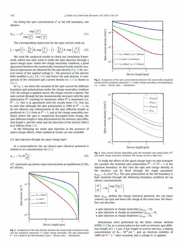
Fig. 2. Comparison of the spin current density between the numerically simulatedresults and the analytical expression (12) under charge neutrality, corresponding toFig. 1 (Lines! Theory, Dots ! Simulation).
Fig. 3. Spin current density depending upon the boundary spin polarization (P0)and under charge neutrality condition. The charge current is kept zero.
118 J. Ghosh et al. / Solid-State Electronics 101 (2014) 116–121
For fixing the spin concentration s0 at the left boundary, oneobtains:
A1ð2Þ ¼ �s0exp �W
LuðdÞ
� �exp W
Lu
� �� exp �W
Ld
� � : ð11Þ
The corresponding expression for the spin current reads as:
Js ¼ qlE 1þ Vth
ELu
� �A2 exp
xLu
� �þ 1� Vth
ELd
� �A1 exp
�xLd
� �� �: ð12Þ
We used the analytical results to check our simulation frame-work, which was later used to study the spin injection through aspace-charge layer. Under the charge neutrality condition, a goodagreement between the numerically simulated results and the ana-lytical expressions are obtained for the spin density (Fig. 1) for sev-eral values of the applied voltage Uc . The presence of the electricfield modifies LuðLdÞ (cf. (10)) and hence the spin density. A com-parison of the simulated spin current density to (12) is shown inFig. 2.
In Fig. 3, we show the variation of the spin current for differentboundary spin polarizations under the charge neutrality condition(CN). No voltage is applied, hence, the charge current is absent. Thespin current through the bar monotonically increases with the spinpolarization P0, reaching its maximum when P0 is maximum (i.e.P0 ¼ 1). This is in agreement with the results from [10]. One hasto note that although the spin polarization is 100% at P0 ¼ 1, wedo not observe any enhancement of the spin diffusion length aspredicted in [10]. Even at P0 ¼ 1, and at the charge neutrality con-dition where the spin is completely decoupled from charge, thespin diffusion length is only determined by the intrinsic spin diffu-sion length L and the value and the direction of the electric field Eas it follows from (10).
In the following we study spin injection in the presence ofspace-charge effects, when analytical results are not available.
2.2. Spin injection through the space-charge layer
In a semiconductor the up (down)-spin chemical potential isrelated to its concentration via [11]:
l"ð#Þ ¼ Vth lnn"ð#Þneql"ð#Þ
: ð13Þ
neql"ð#Þ represents up (down)-spin concentration at equilibrium (0:5ND
for silicon).
Fig. 1. Comparison of the spin density between the numerically simulated resultsand the analytical expression (9) under charge neutrality. The spin polarizationP ¼ 0:5 is fixed at the left boundary (Lines! Theory, Dots ! Simulation).
To study the effects of the space-charge layer on spin transportwe consider the maximal spin polarization P0 ¼ s0=n0 ¼ 1 at theinjection boundary. In this case the spin and charge density atthe interface can be fixed through the single parameterlChem ¼ Vth lnðs0=NDÞ. The spin polarization at the left boundary iskept maximal through the following boundary condition for up(down) concentrations:
n0"
n0#
" #¼ ND
exp lChemVth
� �0
" #: ð14Þ
Here, lChem defines the charge chemical potential. We can inject(release) up-spin and hence the charge at the same time. We there-fore can describe:
� spin injection at charge neutrality (lChem ¼ 0),� spin injection at charge accumulation (lChem > 0),� spin injection at charge depletion (lChem < 0).
Simulations were performed by the finite volume method(FVM) [13] for an n-semiconductor bar with an intrinsic spin diffu-sion length of L = 1 lm. A bar length of several microns, a dopingconcentration of ND ¼ 1016 cm�3, and an electron mobility of1400 cm2 V�1 s�1 were assumed, and a voltage Uc is applied.

J. Ghosh et al. / Solid-State Electronics 101 (2014) 116–121 119
3. Results and discussion
Via (14) a considerable spin and charge accumulation (deple-tion) at the interface can be introduced and hence a spin currentcan diffuse out of this region. The spin and the charge currentthrough the bar can be tuned by varying the chemical potentialand the applied voltage. Charge injection or charge release alwayscause a non-zero charge current in the device, even at the absenceof an external electric field. This charge current can be compen-sated by applying an external voltage, given by the equation:
Uc ¼ �Vth lnn0" þ n0
#
ND
!: ð15Þ
Fig. 5. Variation of the spin current density under boundary condition (14),depicting the presence of an upper saturation at charge accumulation. Chargecurrent is fixed to 11:9MA=m2.
Fig. 6. Spin current density for up to 5 times the Debye length kD from the leftboundary under charge neutrality (CN) and charge accumulation. The chargecurrent is zero. The left boundary for ð1Þ is set with n0 ¼ 1000ND .
3.1. Accumulation: spin current saturation
First, we investigate the carrier distribution and current varia-tion along the bar considering charge accumulation and a fixedcharge current. The charge current density in the bar has beenset to 11:9 MA=m2. The dependence of the charge current densityon the chemical potential (lChem) at varied electric field is depictedin Fig. 4. The voltage applied has to be adjusted in order to keep thecurrent density constant. Strong nonlinear effects due to the con-ductivity variation in the space-charge layer close to the leftboundary cause deviations of the compensating voltage from(15), when the bar moves from accumulation to deep depletion.An abundance of spin carriers during the accumulation enhancesthe spin current close to the interface, while a lack of spin carriersin depletion causes a very strong diminution of the spin current.Fig. 5 reveals that under charge accumulation, the spin currentshows an upper threshold [10]. The amount of the spin currentwhich leaks from the accumulation region almost does not changein high accumulation, regardless of the high value of spin densityand spin current at the interface. This means that an effort to boostthe spin current by increasing the spin concentration at the inter-face to inject more spin polarized electrons does not result in asubstantial spin current increase [10].
In order to further investigate the spin current enhancement (atthe boundaries or in the bulk) due to a charge accumulation, weshow the variation of the spin current for different boundary spinpolarizations. Fig. 6 reveals that for P0 ¼ 1 the spin current close tothe spin injection interface is significantly higher at charge accu-mulation compared to that at CN. However, at a distance of aboutkD from the interface, the spin current becomes similar to that at
Fig. 4. The variation of the charge current density (Jc) as a function of the chemicalpotential defined by (14) and the external voltage (Uc). One extra line also indicatesa constant Jc . The device length is 4 lm.
the interface under CN and the same spin polarization. If P0 < 1,our results indicate that it is not possible to obtain a spin currentin the bulk as high as for P0 ¼ 1, even under higher charge accumu-lation at the interface, and the current is close to that under thecharge neutrality condition with the same P0.
In order to explain this behavior we plot the spin polarization,the charge, and the spin density close to the interface (Fig. 7).The spin polarization remains approximately constant throughthe accumulation layer, while the charge decrease from its highvalue at the interface to the equilibrium value is determined bythe doping concentration ND. Therefore, the spin density alsodecreases substantially. Thus, the spin current in the bulk is deter-mined by the spin density at the end of the accumulation layer,where the charge neutrality condition is restored and is thus deter-mined by the spin current density at the charge neutrality condi-tion with the same spin polarization.
3.2. Depletion: spin current reduction
At depletion, when the spin diffusion is along the current, weobserve a substantial decrease of the spin and the spin current den-sities, both at the interface and the bulk (Fig. 8) as compared to

Fig. 7. Electron concentration and spin density distribution over the line undercharge accumulation with the boundary as in (14), (lChem ¼ 100 mV,Uc ¼ �300 mV). The spin polarization (inset figure) is almost unchanged in thecharge screening region. The charge current is 11:9 MA=m2. The device length is4 lm.
Fig. 9. Spin up (down) current densities and the total spin current density, whenthe device is in depletion. We keep lChem ¼ �100 mV, with Uc ¼ 270 mV forJc ¼ �7:9 MA=m2 and Uc ¼ �24:6 mV for Jc ¼ 7:9 MA=m2.
Fig. 10. Spin current density for accumulation, charge neutrality, and depletionwith the boundary condition (14). The charge current is fixed at �7:9 MA=m2.
120 J. Ghosh et al. / Solid-State Electronics 101 (2014) 116–121
their values at the charge neutrality condition. This behavior is cor-related with a significant increase of the minority spin current inthe depletion layer, cf: Fig. 9. This current is due to two contribu-tions, drift and diffusion, which add constructively in this caseand cause the spin polarization to decrease substantially over avery short distance close to the interface. At the same time, thespin current density remains nearly constant through the depletionlayer. Indeed, in this case the spin diffusion length is increased dueto the high electric field at the depletion region. At the end of thespace-charge layer the spin polarization is thus significantly smal-ler than the one at the interface explaining the spin current degra-dation in the bulk as compared to the one at the charge neutralitycondition. We emphasize again that the sharp decrease of the spinpolarization is due to the high spin minority current close to theinterface. Should this current be reduced, for instance by applyinga voltage of opposite polarity and inverting the current, cf Fig. 9,the spin current in the bulk is enhanced, but still remains belowthe level determined by the charge neutrality condition (Fig. 10).
Therefore, our results indicate that the spin injection throughthe space-charge layer and proper inclusion of screening doesnot result in a spin current enhancement in the bulk in comparisonto the situation under the charge neutrality condition, when the
Fig. 8. Spin and spin current density in depletion(lChem ¼ �100 mV;Uc ¼ �140:4 mV) and the charge neutrality (CN) condition(lChem ¼ 0 mV, Uc ¼ �204:1 mV). The fixed charge current is 11:9 MA=m2. Theinset figure shows the spin polarization. The device length is 4 lm.
space-charge layer is absent, provided the spin polarization atthe interface and the charge currents are kept the same. Comparedto [9] we have ignored here the effective magnetic field in thesemiconductor generated by the injected spins. However, due toits smallness, it is unlikely that this field can drastically alter theresults.
4. Summary and conclusion
Spin injection in a semiconductor structure from a space-chargelayer is considered. At a fixed interface spin polarization, the inter-face spin current is enhanced through injecting more charge, but isalmost unchanged from that obtained at the charge neutrality con-dition in the bulk. In depletion the spin current in the bulk is sup-pressed. Thus, inclusion of the space-charge effects does not resultin a higher spin injection efficiency as compared to the spin injec-tion at the charge neutrality condition, when the spin polarizationat the interface and the charge current are the same. Hence, at afixed polarization, the charge neutrality determines the value ofthe maximum spin current possible provided the charge currentis fixed. Accordingly, the largest spin current at charge neutralityis obtained at maximum spin polarization of the injected carriers,as intuitively expected.

J. Ghosh et al. / Solid-State Electronics 101 (2014) 116–121 121
Acknowledgment
This research is supported by the European Research Councilthrough the Grant #247056 MOSILSPIN.
References
[1] Nikonov DE, Young IA. Overview of beyond-CMOS devices and a uniformmethodology for their benchmarking. Computer 2013;36.
[2] Kim NS, Austin T, Baauw D, Mudge T, Flautner K, Hu JS, et al. Leakage current:moore’s law meets static power. Computer 2003;36(December):68–75. http://dx.doi.org/10.1109/MC.2003.1250885.
[3] Jansen R. Silicon spintronics. Nat. Matter 2012;11(April):400. http://dx.doi.org/10.1038/nmat3293.
[4] Huang Biqin, Monsma Douwe J, Ian Appelbaum. Coherent spin transportthrough a 350 micron thick silicon wafer. Phys. Rev. Lett.2007;99(October):177209. http://dx.doi.org/10.1103/PhysRevLett.99.177209.
[5] Sugahara S, Nitta J. Spin-transistor electronics: an overview and outlook.Proc IEEE 2010;98(October):2124–54. http://dx.doi.org/10.1109/JPROC.2010.2064272.
[6] Song Y, Dery H. Magnetic field modulated resonant tunneling inferromagnetic-insulator-nonmagnetic junctions; 2014 [arXiv/1401.7649].
[7] [7] Txoperena O, Song Y, Qing L, Gobbi M, Hueso LE, Dery H, et al. Universalimpurity-assisted tunneling magnetoresistance under weak magnetic field;2014 [arxiv/1404.0633].
[8] van ’t Erve OMJ, Friedman AL, Cobas E, Li CH, Robinson JT, Jonker BT. Low-resistance spin injection into silicon using graphene tunnel barriers. NatureNano 2012;7:737.
[9] Sears MR, Saslow WM. Spin accumulation at ferromagnet/nonmagneticmaterial interfaces. Phys Rev B 2012;85(January):014404. http://dx.doi.org/10.1103/PhysRevB.85.014404.
[10] Zayets V. Spin and charge transport in materials with spin-dependentconductivity. Phys Rev B 2012;86(November):174415. http://dx.doi.org/10.1103/PhysRevB.86.174415.
[11] Yu ZG, Flatte ME. Spin diffusion and injection in semiconductor structures:electric field effects. Phys Rev B 2002;66(December):235302.
[12] Song Y, Dery H. Spin transport theory in ferromagnet/semiconductorsystems with noncollinear magnetization configurations. Phys Rev B2010;81:045321.
[13] Scharfetter D, Gummel H. Large-signal analysis of a silicon read diodeoscillator. IEEE Trans Electron Dev 1969;16:64. http://dx.doi.org/10.1109/T-ED.1969.16566. ISSN 0018-9383.