speedster22i memoryphy user guide ug043 - achronix · pdf file · 2017-12-15ug043,...
TRANSCRIPT
UG043, April 26, 2014 1
Speedster22i Memory PHY User Guide
UG043 – April 26, 2014
2 UG043, April 26, 2014
Copyright Info
Copyright © 2013 Achronix Semiconductor Corporation. All rights reserved. Achronix is a trademark and Speedster is a registered trademark of Achronix Semiconductor Corporation. All other trademarks are the property of their prospective owners. All specifications subject to change without notice.
NOTICE of DISCLAIMER: The information given in this document is believed to be accurate and reliable. However, Achronix Semiconductor Corporation does not give any representations or warranties as to the completeness or accuracy of such information and shall have no liability for the use of the information contained herein. Achronix Semiconductor Corporation reserves the right to make changes to this document and the information contained herein at any time and without notice. All Achronix trademarks, registered trademarks, and disclaimers are listed at http://www.achronix.com and use of this document and the Information contained therein is subject to such terms.
UG043, April 26, 2014 3
Table of Contents
Copyright Info .................................................................................................... 2
Table of Contents .............................................................................................. 3
Overview ............................................................................................................ 4
DDR PHY ............................................................................................................ 7
Organization and Interfaces ................................................................................................... 7
PHY Structure and Operation .............................................................................................. 10
PHY – Controller Interfacing through Widebus .................................................................... 11
Byte Lane Building Blocks.................................................................................................... 12
TX, RX and OE paths in Data Bits ....................................................................................... 14
DQS Clocking and Circuitry ................................................................................................. 16
DLL Specs and Operation ............................................................................... 17
Revision History .............................................................................................. 20
4 UG043, April 26, 2014
Overview
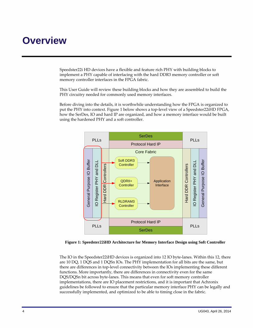
Speedster22i HD devices have a flexible and feature rich PHY with building blocks to implement a PHY capable of interfacing with the hard DDR3 memory controller or soft memory controller interfaces in the FPGA fabric.
This User Guide will review these building blocks and how they are assembled to build the PHY circuitry needed for commonly used memory interfaces.
Before diving into the details, it is worthwhile understanding how the FPGA is organized to put the PHY into context. Figure 1 below shows a top-level view of a Speedster22iHD FPGA, how the SerDes, IO and hard IP are organized, and how a memory interface would be built using the hardened PHY and a soft controller.
Core Fabric
SerDes
SerDes
Protocol Hard IP
Protocol Hard IP
Ge
ne
ral P
urp
ose
IO
Bu
ffe
r
IO R
eg
iste
r P
HY
an
d D
LL
Ha
rd D
DR
Co
ntr
olle
rs
Ge
ne
ral P
urp
ose
IO
Bu
ffe
r
IO R
eg
iste
r P
HY
an
d D
LL
Ha
rd D
DR
Co
ntr
olle
rs
PLLs
PLLs PLLs
PLLs
Soft DDR3
Controller
Application
Interface
QDRII+
Controller
RLDRAM3
Controller
Figure 1: Speedster22iHD Architecture for Memory Interface Design using Soft Controller
The IO in the Speedster22iHD devices is organized into 12 IO byte-lanes. Within this 12, there are 10 DQ, 1 DQS and 1 DQSn IOs. The PHY implementation for all bits are the same, but there are differences in top-level connectivity between the IOs implementing these different functions. More importantly, there are differences in connectivity even for the same DQS/DQSn bit across byte-lanes. This means that even for soft memory controller implementations, there are IO placement restrictions, and it is important that Achronix guidelines be followed to ensure that the particular memory interface PHY can be legally and successfully implemented, and optimized to be able to timing close in the fabric.

UG043, April 26, 2014 5
As stated above, there are 12 IOs in a byte-lane. A group of byte-lanes make up an IO bank and 3 IO banks build an IO cluster (denoted using the initials EN, EC, ES, WN, WC, WS for location). There are a total of 13 byte-lanes (or 156 IOs) per IO cluster, with the IO banks being organized as 2 groups of 4 byte lanes and 1 group of 5 byte lanes.
Every IO cluster is powered by a separate set of power balls and so the power profile and chacteristics of the respective rails will depend on the activity of those specific IOs.
An IO cluster is able to provide no more than 2 clocks (a half-rate and a quarter-rate) to the corresponding triplet of clock regions. For source-synchronous operations where the clock needs to be transmitted from the PHY to the FPGA fabric, the amount of logic that can be clocked using this source-synchronous implementation will be limited by this architecture (unless additional FIFOs/sync logic is used to transfer to a global clock domain in the memory interface PHY). This concept is illustrated in Figure 2 below. Figure 3 shows a blovk level diagram of the IO layout across the FPGA.
Byte
-La
ne
s
0-3
(48
IO
s)
Byte
La
ne
s
4-7
(48
IO
s)
Byte
La
ne
s
8-1
2
(60
IO
s)
Core Fabric
We
st-
No
rth
(W
N)
IO C
luste
r
Clock Region West 1
Clock Region West 2
Clock Region West 3
Figure 2: Speedster22iHD IO Bank and Clock Region Organization for West North Cluster

6 UG043, April 26, 2014
Core Fabric
WN
IO
Clu
ste
r
WN
Ha
rd D
DR
3
Co
ntr
olle
r
WC
IO
Clu
ste
r
WC
Ha
rd D
DR
3
Co
ntr
olle
r
WS
IO
Clu
ste
r
WS
Ha
rd D
DR
3
Co
ntr
olle
r
EN
Ha
rd D
DR
3
Co
ntr
olle
r
EC
Ha
rd D
DR
3
Co
ntr
olle
r
ES
Ha
rd D
DR
3
Co
ntr
olle
r
EN
IO
Clu
ste
r
EC
IO
Clu
ste
r
ES
IO
Clu
ste
r
Figure 3: Speedster22iHD IO Cluster Organization
The next sections will discuss the actual PHY implementation for the different memory interfaces in more detail.
UG043, April 26, 2014 7
DDR PHY
Organization and Interfaces
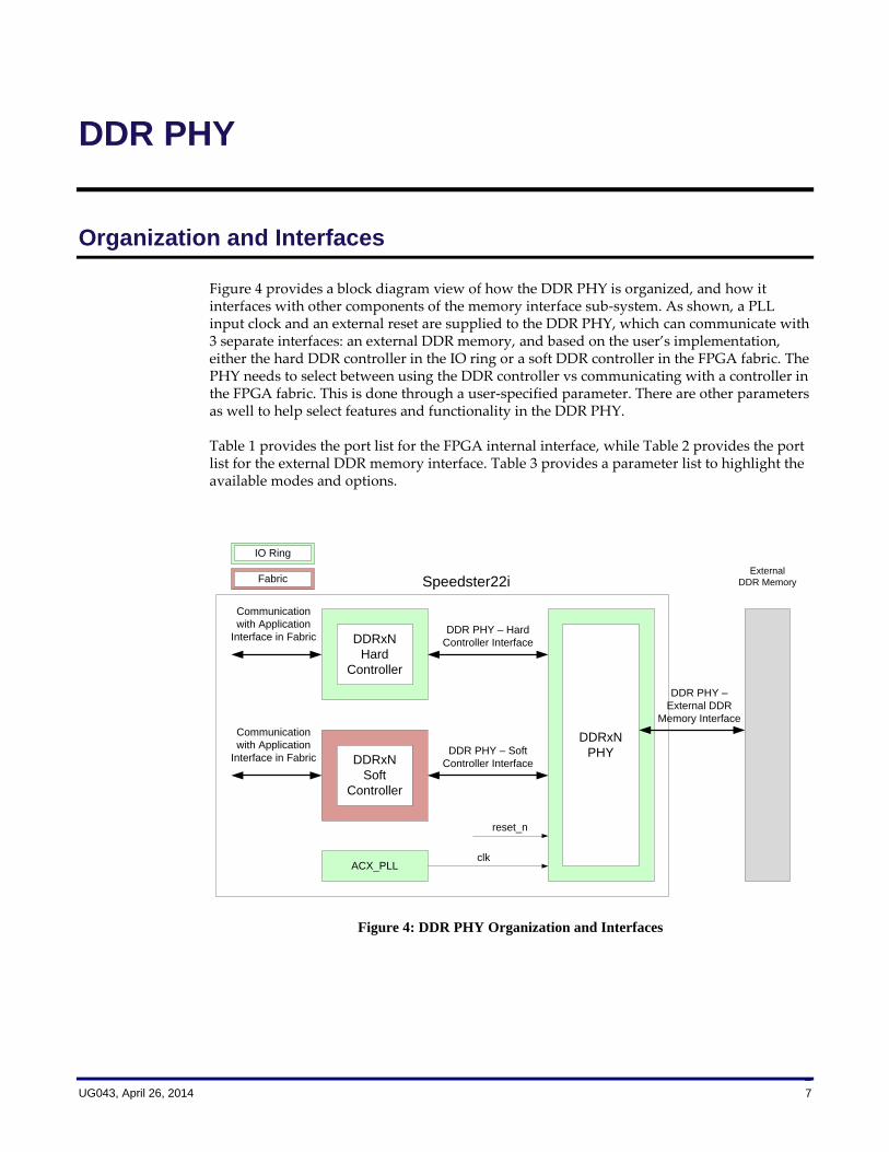
Figure 4 provides a block diagram view of how the DDR PHY is organized, and how it interfaces with other components of the memory interface sub-system. As shown, a PLL input clock and an external reset are supplied to the DDR PHY, which can communicate with 3 separate interfaces: an external DDR memory, and based on the user’s implementation, either the hard DDR controller in the IO ring or a soft DDR controller in the FPGA fabric. The PHY needs to select between using the DDR controller vs communicating with a controller in the FPGA fabric. This is done through a user-specified parameter. There are other parameters as well to help select features and functionality in the DDR PHY.
Table 1 provides the port list for the FPGA internal interface, while Table 2 provides the port list for the external DDR memory interface. Table 3 provides a parameter list to highlight the available modes and options.
Speedster22i
ACX_PLLclk
DDRxN
PHY
External
DDR Memory
DDRxN
Hard
Controller
DDRxN
Soft
Controller
Communication
with Application
Interface in Fabric
Communication
with Application
Interface in Fabric
IO Ring
Fabric
DDR PHY – Soft
Controller Interface
DDR PHY – Hard
Controller Interface
DDR PHY –
External DDR
Memory Interface
reset_n
Figure 4: DDR PHY Organization and Interfaces
8 UG043, April 26, 2014
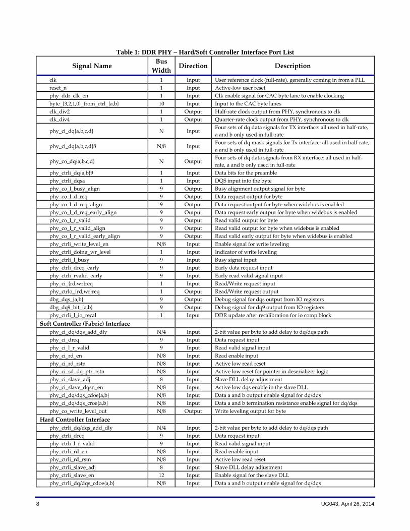
Table 1: DDR PHY – Hard/Soft Controller Interface Port List
Signal Name Bus
Width Direction Description
clk 1 Input User reference clock (full-rate), generally coming in from a PLL
reset_n 1 Input Active-low user reset
phy_ddr_clk_en 1 Input Clk enable signal for CAC byte lane to enable clocking
byte_{3,2,1,0}_from_ctrl_{a,b} 10 Input Input to the CAC byte lanes
clk_div2 1 Output Half-rate clock output from PHY, synchronous to clk
clk_div4 1 Output Quarter-rate clock output from PHY, synchronous to clk
phy_ci_dq{a,b,c,d} N Input Four sets of dq data signals for TX interface: all used in half-rate,
a and b only used in full-rate
phy_ci_dq{a,b,c,d}8 N/8 Input Four sets of dq mask signals for Tx interface: all used in half-rate,
a and b only used in full-rate
phy_co_dq{a,b,c,d} N Output Four sets of dq data signals from RX interface: all used in half-
rate, a and b only used in full-rate
phy_ctrli_dq{a,b}9 1 Input Data bits for the preamble
phy_ctrli_dqsa 1 Input DQS input into the byte
phy_co_l_busy_align 9 Output Busy alignment output signal for byte
phy_co_l_d_req 9 Output Data request output for byte
phy_co_l_d_req_align 9 Output Data request output for byte when widebus is enabled
phy_co_l_d_req_early_align 9 Output Data request early output for byte when widebus is enabled
phy_co_l_r_valid 9 Output Read valid output for byte
phy_co_l_r_valid_align 9 Output Read valid output for byte when widebus is enabled
phy_co_l_r_valid_early_align 9 Output Read valid early output for byte when widebus is enabled
phy_ctrli_write_level_en N/8 Input Enable signal for write leveling
phy_ctrli_doing_wr_level 1 Input Indicator of write leveling
phy_ctrli_l_busy 9 Input Busy signal input
phy_ctrli_dreq_early 9 Input Early data request input
phy_ctrli_rvalid_early 9 Input Early read valid signal input
phy_ci_{rd,wr}req 1 Input Read/Write request input
phy_ctrlo_{rd,wr}req 1 Output Read/Write request output
dbg_dqs_{a,b} 9 Output Debug signal for dqs output from IO registers
dbg_dq9_bit_{a,b} 9 Output Debug signal for dq9 output from IO registers
phy_ctrli_l_io_recal 1 Input DDR update after recalibration for io comp block
Soft Controller (Fabric) Interface
phy_ci_dq/dqs_add_dly N/4 Input 2-bit value per byte to add delay to dq/dqs path
phy_ci_dreq 9 Input Data request input
phy_ci_l_r_valid 9 Input Read valid signal input
phy_ci_rd_en N/8 Input Read enable input
phy_ci_rd_rstn N/8 Input Active low read reset
phy_ci_sd_dq_ptr_rstn N/8 Input Active low reset for pointer in deserializer logic
phy_ci_slave_adj 8 Input Slave DLL delay adjustment
phy_ci_slave_dqsn_en N/8 Input Active low dqs enable in the slave DLL
phy_ci_dq/dqs_cdoe{a,b} N/8 Input Data a and b output enable signal for dq/dqs
phy_ci_dq/dqs_croe{a,b} N/8 Input Data a and b termination resistance enable signal for dq/dqs
phy_co_write_level_out N/8 Output Write leveling output for byte
Hard Controller Interface
phy_ctrli_dq/dqs_add_dly N/4 Input 2-bit value per byte to add delay to dq/dqs path
phy_ctrli_dreq 9 Input Data request input
phy_ctrli_l_r_valid 9 Input Read valid signal input
phy_ctrli_rd_en N/8 Input Read enable input
phy_ctrli_rd_rstn N/8 Input Active low read reset
phy_ctrli_slave_adj 8 Input Slave DLL delay adjustment
phy_ctrli_slave_en 12 Input Enable signal for the slave DLL
phy_ctrli_dq/dqs_cdoe{a,b} N/8 Input Data a and b output enable signal for dq/dqs

UG043, April 26, 2014 9
Signal Name Bus
Width Direction Description
phy_ctrli_dq/dqs_croe{a,b} N/8 Input Data a and b termination resistance enable signal for dq/dqs
phy_ctrlo_write_level_out N/8 Output Write leveling output for byte
Table 2: DDR PHY External Memory Interface Port List
Signal Name Bus
Width Direction Description
sd_clk_p 3 Output SDRAM differential clock signal (positive polarity)
sd_clk_n 3 Output SDRAM differential clock signal (negative polarity)
sd_cke 4 Output SDRAM clock enable control signal
sd_odt 4 Output SDRAM on die termination control signal
sd_ras_n 1 Output SDRAM RAS control signal
sd_cas_n 1 Output SDRAM CAS control signal
sd_we_n 1 Output SDRAM write enable control signal
sd_reset_n 1 Output SDRAM reset signal
sd_a 16 Output SDRAM address bus
sd_ba 3 Output SDRAM bank select
sd_cs_n 4 Output SDRAM chip select
sd_dm N/8 Inout SDRAM data mask
sd_dummy N/8 Inout Internal use only. Leave unconnected.
sd_dq N Inout SDRAM data bus
sd_dqsn N/8 Inout SDRAM DQS bus, which is used to clock DQ bus
sd_dqsp N/8 Inout SDRAM DQS bus, which is used to clock DQ bus
Table 3: DDR PHY Parameter List
Parameter Default (hex) Valid Values Description
DSIZE 16 Multiples of 8 up to 72 Local side data width
USE_CONTROLLER D̀EF_USE_CONTROLLER D̀EF_USE_CONTROLLER,
D̀EF_NOT_USE_CONTROLLER Specifies whether the hard controller
should be used in the design
NUM_CLK_OUTS 4 1 to 4 Number of clock outputs
NUM_RANKS 1 1 to 4 Number of memory ranks in system
BYPASS_TXRX_SD D̀EF_IO_RXSD_BYPASS_MUX D̀EF_IO_RXSD_BYPASS_MUX
D̀EF_IO_RXSD_NO_BYPASS_MUX Specifies data at full-rate vs half-rate
(Bypass=Full-rate, No_bypass=Half-rate)
EXTRA_PIPELINE_N 1'b1 1'b0, 1'b1
0 -> One extra clock cycle to load data
1 -> No extra cycle
Applies to both read and write paths
EXTRA_1CLK_DLY 0 0, 1 1 -> extra one clock delay in 2X mode.
WIDE_BUS 0 0, 1
1 -> Wide-bus used in fabric to convert
incoming data to quarter-rate. PHY
provides quarter-rate clock on clk_div4.
BYTE_LANE[N/8-1:0]_DLL_ADJ_DQ 6'h04 6’h00 to 6’hFF DQ Slave adjust for BYTE_LANE
BYTE_LANE[N/8-1:0]_DLL_ADJ_DQS 6'h16 6’h00 to 6’hFF DQS Slave adjust for BYTE_LANE
BYTE_LANE[N/8-1:0]_DLL_ADJ_DP 6'h04 6’h00 to 6’hFF DP Slave adjust for BYTE_LANE
BYTE_LANE[N/8-
1:0]_WR_LVL_DQ_SELECT `WLVL_SELECT_DQ0
`WLVL_SELECT_DQ0 up to
`WLVL_SELECT_DQ7 DQ bit used for write leveling
BYTE_LANE_DLL_DQSX9_CLK_ADJ 6'h10 6’h00 to 6’hFF DLL adjust for wpb_tx_dqsx9_clk(0.25T)
BYTE_LANE_DLL_DQX9_CLK_ADJ 6'h30 6’h00 to 6’hFF DLL adjust for wpb_tx_dqx9_clk(0.75T)
BYTE_LANE_CAC_DLL_ADJ_DQSN 6'h17 6’h00 to 6’hFF DP Slave adj for CAC byte lanes (0.35T)
10 UG043, April 26, 2014
PHY Structure and Operation
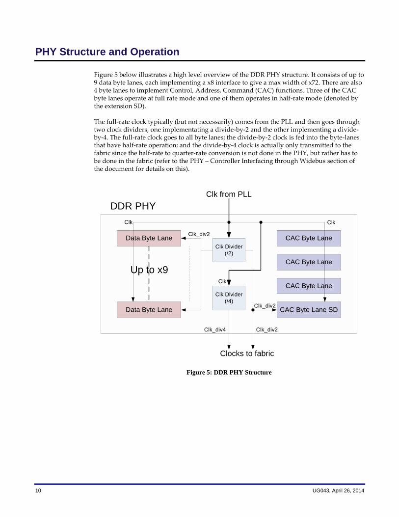
Figure 5 below illustrates a high level overview of the DDR PHY structure. It consists of up to 9 data byte lanes, each implementing a x8 interface to give a max width of x72. There are also 4 byte lanes to implement Control, Address, Command (CAC) functions. Three of the CAC byte lanes operate at full rate mode and one of them operates in half-rate mode (denoted by the extension SD).
The full-rate clock typically (but not necessarily) comes from the PLL and then goes through two clock dividers, one implementating a divide-by-2 and the other implementing a divide-by-4. The full-rate clock goes to all byte lanes; the divide-by-2 clock is fed into the byte-lanes that have half-rate operation; and the divide-by-4 clock is actually only transmitted to the fabric since the half-rate to quarter-rate conversion is not done in the PHY, but rather has to be done in the fabric (refer to the PHY – Controller Interfacing through Widebus section of the document for details on this).
Data Byte Lane
Data Byte Lane
CAC Byte Lane
CAC Byte Lane
CAC Byte Lane
CAC Byte Lane SD
Clk Divider
(/2)
Clk Divider
(/4)
Clk from PLL
Clocks to fabric
Clk_div2
Clk_div4
Clk_div2
DDR PHY
Up to x9
Clk Clk
Clk_div2
Clk
Figure 5: DDR PHY Structure
UG043, April 26, 2014 11
PHY – Controller Interfacing through Widebus
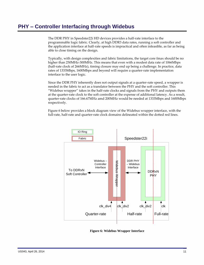
The DDR PHY in Speedster22i HD devices provides a half-rate interface to the programmable logic fabric. Clearly, at high DDR3 data rates, running a soft controller and the application interface at half-rate speeds is impractical and often infeasible, as far as being able to close timing on the design.
Typically, with design complexities and fabric limitations, the target core fmax should be no higher than 250MHz-300MHz. This means that even with a modest data rate of 1066Mbps (half-rate clock of 266MHz), timing closure may end up being a challenge. In practice, data rates of 1333Mbps, 1600Mbps and beyond will require a quarter-rate implementation interface to the user logic.
Since the DDR PHY inherently does not output signals at a quarter-rate speed, a wrapper is needed in the fabric to act as a translator between the PHY and the soft controller. This “Widebus wrapper” takes in the half-rate clocks and signals from the PHY and outputs them at the quarter-rate clock to the soft controller at the expense of additional latency. As a result, quarter-rate clocks of 166.67MHz amd 200MHz would be needed at 1333Mbps and 1600Mbps respectively.
Figure 6 below provides a block diagram view of the Widebus wrapper interface, with the full-rate, half-rate and quarter-rate clock domains delineated within the dotted red lines.
Speedster22i
DDRxN
PHY
IO Ring
Fabric
DDR PHY
– Widebus
Interface
Wid
eb
us W
rap
pe
r
Widebus –
Controller
Interface
clk_div4 clk_div2 clk_div2 clk
Quarter-rate Half-rate Full-rate
To DDRxN
Soft Controller
Figure 6: Widebus Wrapper Interface

12 UG043, April 26, 2014
Byte Lane Building Blocks
As shown in Figure 5, the DDR PHY is made up of up to 9 data byte lanes (for a x72 mode interface) and 4 CAC (Control, Address and Command) byte lanes, 1 one of them operating at half rate, as denoted by the SD postfix. The building blocks inside these byte lanes are very similar. This section will detail the building blocks in a data byte lane and then explain the differences that can be seen in a CAC byte lane.
Figure 7 below provides a block level diagram of the building blocks inside a data byte lane. Each of these blocks are described in more detail below.
ddr3_dq_bit
ddr3_dq_bit
x8
ddr3_dm_bit
ddr3_dq9_bit postamble ddr3_dqs_bit
Clk_mux
byte_lane_rxsy
write-leveling circuitry
byte
_la
ne
_sd_
log
ic
DLL
(0.75T)
DLL
(0.25T)
byte
_la
ne
_lo
gic
DDR3 Data Byte Lane
Figure 7: DDR3 Data Byte Lane Building Blocks
Clk_mux: As the name implies, the clock mux takes in clocks coming in from the PLL, selects and distributes them to the rest of the PHY logic.
ddr3_dq_bit: There are 8 of these dq data modules which feed the bidirectional buffers used in data transmission and reception. The chapter on TX, RX and OE paths in Data Bits provides a much closer look at the data paths through these dq data modules.
ddr3_dm_bit: This is the data mask bit controlling the masking operation at a byte level into the PHY.
UG043, April 26, 2014 13
ddr3_dq9_bit/postamble/ddr3_dqs_bit: These are the modules used to transmit and receive dqs pulses to sample the data at dq. The chapter on DQS Clocking and Circuitry provides more detail about the functionality of each of these blocks and how the dqs is adjusted to ensure that the dq data is sampled optimally. The dqs output is provided to all of the dq and dm bits as a clock. It can also be routed as an output to the FPGA fabric.
write leveling circuitry: There are 2 slave DLLs (sdlls), denoted as 0.25T and 0.75T to help provide mechanisms to enable write leveling. These two DLLs take the reference clock as input and produce shifted versions of this clock as inputs to the first stage of registering in the dqs TX path.
byte_lane_rxsy: This module takes clocks and enables from the fabric as inputs and uses them to time and generate the write and read pointers that are used when doing clock domain transferring between the dqs clock domain and the core clock domain in the hard FIFO on the data receive path.
byte_lane_logic/byte_lane_sd_logic: These modules provide control interfaces for muxing signals between the hard DDR controller and a soft DDR controller (from the fabric).
A CAC byte lane is much simpler in its structure. There is a single bit module for every pad that needs to be placed. A slave dll is used to provide for leveling capability and there is an option to use a pad to have source synchronous clock be routed into the fabric. No additional masking, pre/postambles or muxing is implemented or needed.
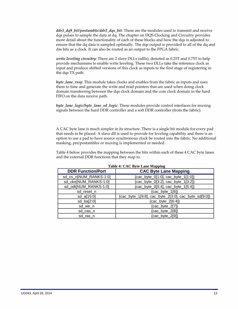
Table 4 below provides the mapping between the bits within each of these 4 CAC byte lanes and the external DDR functions that they map to.
Table 4: CAC Byte Lane Mapping
DDR Function/Port CAC Byte Lane Mapping
sd_cs_n[NUM_RANKS-1:0] {cac_byte_0[1:0], cac_byte_1[1:0]}
sd_cke[NUM_RANKS-1:0] {cac_byte_0[3:2], cac_byte_1[3:2]}
sd_odt[NUM_RANKS-1:0] {cac_byte_0[5:4], cac_byte_1[5:4]}
sd_reset_n {cac_byte_1[6]}
sd_a[15:0] {cac_byte_1[9:8], cac_byte_2[3:0], cac_byte_sd[9:0]}
sd_ba[2:0] {cac_byte_2[6:4]}
sd_we_n {cac_byte_2[7]}
sd_cas_n {cac_byte_2[8]}
sd_ras_n {cac_byte_2[9]}

14 UG043, April 26, 2014
TX, RX and OE paths in Data Bits
This section highlights the pieces of the TX, RX and OE circuitry that make up each of the data bits. These same pieces are also used in building clock, dqs and dm bits also, and the flexibility provided enables more custom IO configurations to be created as well. Figure 8 shows a block level diagram of the TX, RX and OE paths. The paths and the modules used are described in more detail below.
DQ PAD
rx_anyipbit_y
sdll
rx_fifo
rx_sd
tx_anyopbit_data_out
tx_flop
tx_sd
oeren_any
opbit_oe
oeren_flop
opbit_rtt
Figure 8: TX, RX and OE paths in a DDR DQ bit
Receive path: Data coming from the DQ pad goes through the receive buffer and is then provided as an input to the rx_any module. This data then goes through a slave dll (sdll) which is essentially used to implement read-leveling. The output of the sdll is then fed into the rx_fifo module which contains a fifo of depth four (at full-rate). At this point, the receive data is sampled at the positive and negative edges for full-rate conversion, and a clock domain transfer take place in the fifo between the dqs clock domain and the full-rate clock domain coming from the FPGA PLL. The output of the rx_fifo is then optionally fed into a rx_sd module which implements a full-rate to half-rate conversion prior to transferring the four-wide data into the fabric.
UG043, April 26, 2014 15
Transmit path: If half-rate (or quarter-rate with the widebus wrapper) is used in the fabric, four-wide data is provided from the fabric to a tx_sd module. The tx_sd module converts the incoming data from half-rate to full-rate and provides a two-wide data into the tx_any module (tx_sd module should be bypassed if a full-rate interface is used in the fabric). The data passes from the tx_any module into the tx_flop module, which samples the transmit data at both the positive and negative edges of the full-rate clock and aligns the data to the dqs clock domain. This data is then passed to the transmit buffer before being sent out on the pad.
Output Enable path: Full-rate output enables are passed from the fabric to the oeren_ny module which passes the data to the oeren_flop. Similar to the tx_flop implementation, oeren_flop samples the oe data at both the positive and negative edges of the full-rate clock and aligns the data to the dqs clock domain. This is then fed as an output enable signal to the transmit buffer. In addition, there is a termination resistance enable signal, opbit_rtt, that goes through essentially the same path as the oe data, to turn on/off the input buffer impedance when reading vs writing data.
16 UG043, April 26, 2014
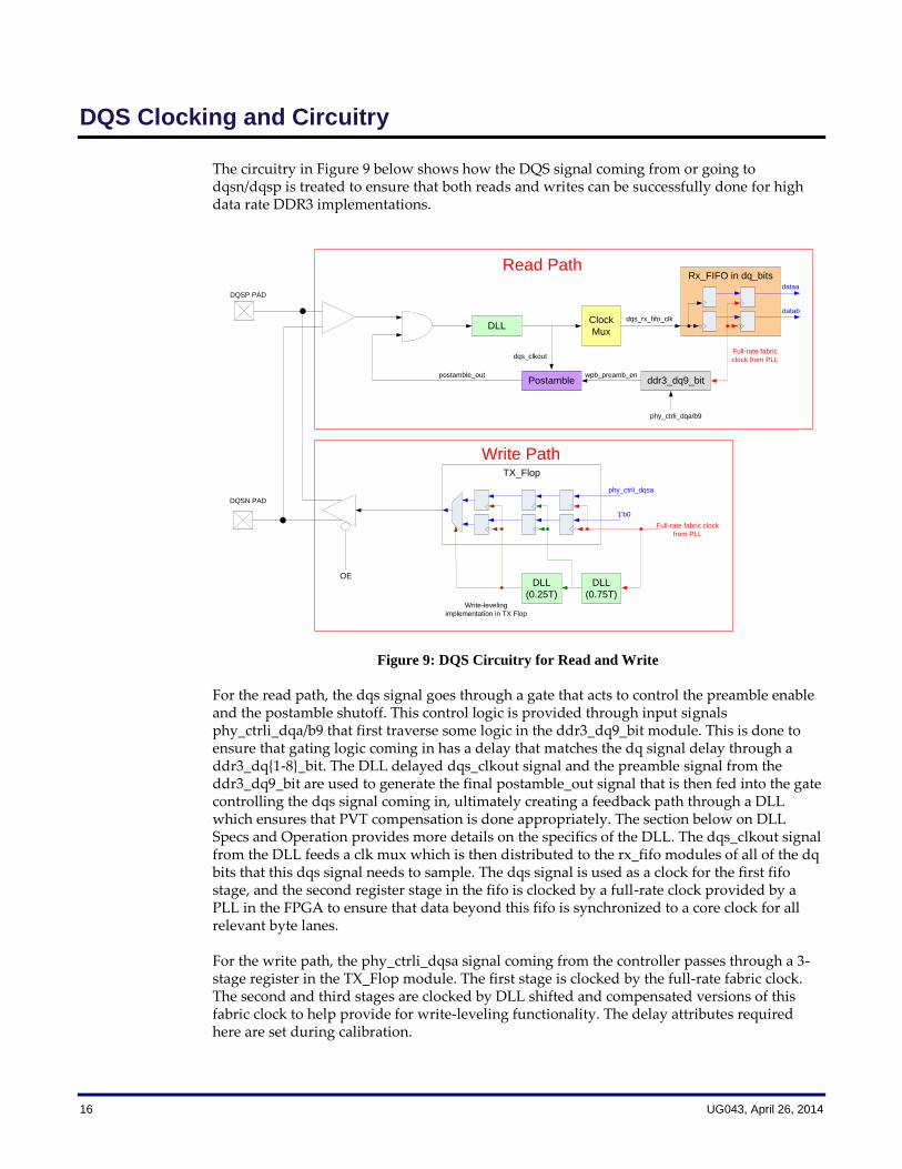
DQS Clocking and Circuitry
The circuitry in Figure 9 below shows how the DQS signal coming from or going to dqsn/dqsp is treated to ensure that both reads and writes can be successfully done for high data rate DDR3 implementations.
DQSP PAD
DQSN PAD
OE
DLLClock
Mux
Rx_FIFO in dq_bitsdataa
databdqs_rx_fifo_clk
Full-rate fabric
clock from PLL
Postamble
dqs_clkout
postamble_outddr3_dq9_bit
wpb_preamb_en
phy_ctrli_dqa/b9
TX_Flop
DLL
(0.75T)
DLL
(0.25T)
phy_ctrli_dqsa
1'b0
Full-rate fabric clock
from PLL
Write-leveling
implementation in TX Flop
Read Path
Write Path
Figure 9: DQS Circuitry for Read and Write
For the read path, the dqs signal goes through a gate that acts to control the preamble enable and the postamble shutoff. This control logic is provided through input signals phy_ctrli_dqa/b9 that first traverse some logic in the ddr3_dq9_bit module. This is done to ensure that gating logic coming in has a delay that matches the dq signal delay through a ddr3_dq{1-8}_bit. The DLL delayed dqs_clkout signal and the preamble signal from the ddr3_dq9_bit are used to generate the final postamble_out signal that is then fed into the gate controlling the dqs signal coming in, ultimately creating a feedback path through a DLL which ensures that PVT compensation is done appropriately. The section below on DLL Specs and Operation provides more details on the specifics of the DLL. The dqs_clkout signal from the DLL feeds a clk mux which is then distributed to the rx_fifo modules of all of the dq bits that this dqs signal needs to sample. The dqs signal is used as a clock for the first fifo stage, and the second register stage in the fifo is clocked by a full-rate clock provided by a PLL in the FPGA to ensure that data beyond this fifo is synchronized to a core clock for all relevant byte lanes.
For the write path, the phy_ctrli_dqsa signal coming from the controller passes through a 3-stage register in the TX_Flop module. The first stage is clocked by the full-rate fabric clock. The second and third stages are clocked by DLL shifted and compensated versions of this fabric clock to help provide for write-leveling functionality. The delay attributes required here are set during calibration.

UG043, April 26, 2014 17
DLL Specs and Operation
The DLL IP block in the Speedster22i HD1000 is wide range DLL with 1 Master DLL (MDLL) and 12 Slave DLLs (SDLLs). Table 5 provides the DLL IP Specs and Figure 10 provides a high-level block diagram of the DLL architecture.
Table 5: DLL IP Specs
Performance Parameters Data
Frequency Range 311MHz– 1066 MHz
Max P2P period jitter @ 2133MHz with noise freq = 200Mhz and +/-15mV sinusoidal noise
<2% of cycle time
Minimum high low slave pulse width 25% reference cycle
DLL Lock time < 500 reference clock cycles
SDLL Step size 360/64 degrees nominal
Output phase accuracy +/- 4% reference clock cycle
Output phase resolution 6 bits
Slave delay adjustment 0% to 100% of reference cycle
Number of outputs per lane 1
Number of lanes per master 12
Reference Input Duty Cycle 40% - 60%
Master DLL
Slave DLL
Lock Detector
Startup Timer
View
Block
Pbias Nbias
input reference
CLK
data_in<11:0>
sdll_out<11:0>
pin out
Figure 10: DLL Architecture High-Level Block Diagram

18 UG043, April 26, 2014
The MDLL uses a regulated supply generated by a high performance on-board regulator to achieve the best possible performance in terms of jitter. It gets a clock as its reference to generate desired delay in its delay cells. The delay cells used in its VCDL is based on a current starved technique to provide the delay to generate the feedback signal. The phase of the feedback signal is compared with the reference signal. This phase difference is translated to voltage (PBIAS and NBIAS) by the phase detector and charge pump, which is given back to the VCDL block to generate the required delay by either pushing out or pulling in the feedback clock to reduce the phase error between the reference clock and the feedback clock. The VCDL has 16 delay elements, and each delay cell provides 22.5 deg phase difference in locked condition. As there are 16 delay cells in series, the out signal of the 16th delay cell will have a 360 degrees phase offset with respect to the reference clock. Figure 11 below shows a block diagram of the MDLL.
Delay Cell Block
ph360
Start-up Phase detector Charge PumpBias Generator
Lo
op
Filt
er
ph0up
dnOpenloop_sel
Master
enable
PLL CLK
Front
buffer
16th Delay
cell
1st
Delay
cell
Load
buffer
ph0 ph45 ph90 ph135 ph180 ph225 ph270 ph315
Pbias
Nbias
Figure 11: MDLL Block Diagram
The SDLL and the phase interpolator are used to adjust the delay of the strobe signal and data signals in the data module so that they will be aligned. The phase interpolator gets 17 clocks with a phase separation of 22.5 degrees from the SDLL, and then performs fine tuning by mixing various phases as determined by the programmable config bit settings. The phase interpolator has two stages of mixing the clock. In the first stage it performs coarse tuning through a mux by selecting the ph0 and ph1 option list as shown in Table 6.
Table 6: Phase Interpolator Mux Output List
Mux Output Option Ph0 Ph1
1 0 22.5
2 22.5 45
3 45 67.5
4 67.5 90
5 90 112.5
6 112.5 135
7 135 157.5
8 157.5 180

UG043, April 26, 2014 19
Mux Output Option Ph0 Ph1
9 180 202.5
10 202.5 225
11 225 247.5
12 247.5 270
13 270 292.5
14 292.5 315
15 315 337.5
16 337.5 360
In the second stage the phase interpolator mixes the two phases (ph0 and ph1) mentioned above to meet the required delay/phase difference. For example, to push out the incoming signal by a 100 degree phase, the first stage selects phase 90 and phase 112.5, and then the second stage uses this pair and fine tunes it to meet the required 100 degree push out. Figure 12 below provides a block diagram of the SDLL and Phase Interpolator.
Slave DLL
Course selection of clocks
Through Muxs
Fine Selection through
Programmable drive
strength
Phase Interpolator Block per clock
Pbias
Nbias
Bias from MDLL
Decoder
LSB[3:0]MSB[16:0]Phase
Interpolator
Codes<5:0>
Phase
Interpolator
Clock out
17
Figure 12: SDLL and Phase Interpolator Block Diagram
20 UG043, April 26, 2014
Revision History
The following table shows the revision history for this document.
Date Version Revisions
04/26/2014 1.0 Initial Achronix release.