specification for bthq 128064avd-sre-06-cog · vl-fs-cog-btd12864-01 rev. a (bthq...
TRANSCRIPT

www.data-modul.deDATA MODUL AG Landsberger Str. 322 80687 München Tel.: 089/ 56017-0 Fax 089/ 56017-119
BATRON
0
Specification for
Version July 2003
BTHQ 128064AVD-SRE-06-COG
VL-FS-COG-BTD12864-01 REV. A(BTHQ 128064AVD-SRE-06-COG)
JULY/2003
PAGE 2 OF 16
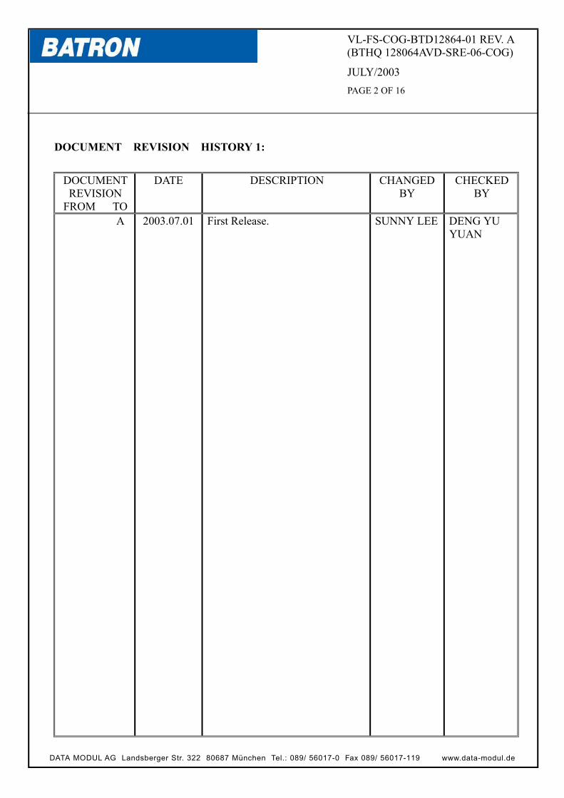
DOCUMENT REVISION HISTORY 1:
DOCUMENTREVISION
FROM TO
DATE DESCRIPTION CHANGED BY
CHECKEDBY
A 2003.07.01 First Release. SUNNY LEE DENG YU YUAN
www.data-modul.deDATA MODUL AG Landsberger Str. 322 80687 München Tel.: 089/ 56017-0 Fax 089/ 56017-119

VL-FS-COG-BTD12864-01 REV. A(BTHQ 128064AVD-SRE-06-COG)
JULY/2003
PAGE 3 OF 16
CONTENTS
Page No. 1. GENERAL DESCRIPTION 4 2. MECHANICAL SPECIFICATIONS 4 3. INTERFACE SIGNALS 9 4. ABSOLUTE MAXIMUM RATINGS 11 4.1 ELECTRICAL MAXIMUM RATINGS (Ta=25¯C) 11 4.2 ENVIRONMENTAL CONDITION 11 5. ELECTRICAL SPECIFICATIONS 12 5.1 TYPICAL ELECTRICAL CHARACTERISTICS 12 5.2 TIMING SPECIFICATIONS 13 6. COMMAND TABLE 16
www.data-modul.deDATA MODUL AG Landsberger Str. 322 80687 München Tel.: 089/ 56017-0 Fax 089/ 56017-119

VL-FS-COG-BTD12864-01 REV. A(BTHQ 128064AVD-SRE-06-COG)
JULY/2003
PAGE 4 OF 16
Specificationof
LCD Module Type Model No.: COG-BTD12864-01
1. General Description
¶ 128 x 64 Dots STN Positive Yellow Reflective Dot Matrix LCD Module.
¶ Viewing Angle: 12 o’clock direction.
¶ Driving duty: 1/65 Duty, 1/7 bias.
¶ ‘Epson’ S1D10605D04B (COG) Dot Matrix LCD Driver or equivalent.
¶ FPC
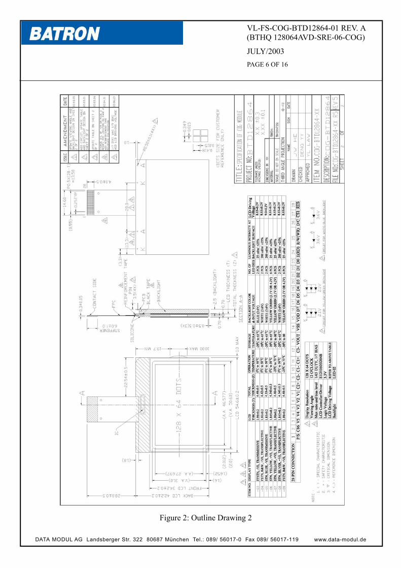
2. Mechanical Specifications
The mechanical detail is shown in Fig. 1 and summarized in Table 1 below.
Table 1
Parameter Specifications Unit Outline dimensions 55.6(W) x 70.2(H) x 1.095(D) (Included FPC) mm Viewing area 50.60(W) x 31.0(H) mm Active area 46.577(W) x 27.697(H) mm Display format 128(W) x 64(H) dots Dot size 0.349(W) x 0.418(H) mm Dot spacing 0.015(W) x 0.015(H) mm Dot pitch 0.364(W) x 0.433(H) mm Weight Approx. 9 grams
www.data-modul.deDATA MODUL AG Landsberger Str. 322 80687 München Tel.: 089/ 56017-0 Fax 089/ 56017-119

VL-FS-COG-BTD12864-01 REV. A(BTHQ 128064AVD-SRE-06-COG)
JULY/2003
PAGE 5 OF 16
Figure 1: Outline Drawing 1
www.data-modul.deDATA MODUL AG Landsberger Str. 322 80687 München Tel.: 089/ 56017-0 Fax 089/ 56017-119
VL-FS-COG-BTD12864-01 REV. A(BTHQ 128064AVD-SRE-06-COG)
JULY/2003
PAGE 6 OF 16
Figure 2: Outline Drawing 2
www.data-modul.deDATA MODUL AG Landsberger Str. 322 80687 München Tel.: 089/ 56017-0 Fax 089/ 56017-119

VL-FS-COG-BTD12864-01 REV. A(BTHQ 128064AVD-SRE-06-COG)
JULY/2003
PAGE 7 OF 16
COG-BTD12864 LCD GRAPHIC DISPLAY
128X64 DOTS
128
32
32
V2
V1
R/W(WR)
D/C
DOT MATRIXLCD
CONTROLLER/DRIVER
'EPSON'S1D10605D04B
(COG)
V4
E(RD)
VSS
VDD
V5
V3
C2+
C1-
C1+
C2-
C3-
VOUT
8D7~D0
CS1
RES
C86
P/S
Figure 3: Block Diagram.
www.data-modul.deDATA MODUL AG Landsberger Str. 322 80687 München Tel.: 089/ 56017-0 Fax 089/ 56017-119

VL-FS-COG-BTD12864-01 REV. A(BTHQ 128064AVD-SRE-06-COG)
JULY/2003
PAGE 8 OF 16
Figure 4: Reference Circuit
www.data-modul.deDATA MODUL AG Landsberger Str. 322 80687 München Tel.: 089/ 56017-0 Fax 089/ 56017-119

VL-FS-COG-BTD12864-01 REV. A(BTHQ 128064AVD-SRE-06-COG)
JULY/2003
PAGE 9 OF 16
3. Interface signals
Table 2(a): Pin Assignment
Pin No. Symbol Description 1 P/S This is the parallel data input/serial data input switch terminal.
P/S = HIGH: Parallel data input. P/S = LOW: Serial data input.
The following applies depending on the P/S status: P/S Data/Command Data Read/Write Serial Clock
HIGH D/C(A0) D0 to D7 RD, WR LOW D/C(A0) SI (D7) Write only SCL (D6)
When P/S = LOW, D0 to D5 are HZ. D0 to D5 may be HIGH, LOW or Open. RD(E) and WR(R/W) are fixed to either HIGH or LOW. With serial data input, RAM display data reading is not supported.
2 C86 This is the MPU interface switch terminal. C86=HIGH: 6800 Series MPU interface. C86=LOW: 8080 MPU interface.
3 V5 4 V4 5 V3 6 V2 7 V1
This is multi-level power supply for liquid crystal drive. Voltage levels are determined based on VDD, and must maintain the relative magnitudes shown below. VDD (=V0) V1 V2 V3 V4 V5
Master operation When the power supply turns ON, the internal power supply circuits produce V1 to V4 voltages shown below. The voltage setting are selected using the LCD bias set command.
For 1/7 bias: V1=(1/7)xV5, V2=(2/7)xV5, V3=(5/7)xV5, V4=(6/7)xV5. 8 C2+ DC/DC voltage converter. Connects a capacitor between this terminal and C2–
terminal. 9 C2- DC/DC voltage converter. Connects a capacitor between this terminal and C2+
terminal. 10 C1- DC/DC voltage converter. Connects a capacitor between this terminal and C1+
terminal. 11 C1+ DC/DC voltage converter. Connects a capacitor between this terminal and C1–
terminal. 12 C3- DC/DC voltage converter. Connects a capacitor between this terminal and C1+
terminal. 13 VOUT DC/DC voltage converter. Connects a capacitor between this terminal and VSS. 14 VSS 0 V pin connected to the system ground (GND) and this is also the reference
power supply for the step-up voltage circuit for the liquid crystal drive. 15 VDD Power supply for logic(+3.3V).
www.data-modul.deDATA MODUL AG Landsberger Str. 322 80687 München Tel.: 089/ 56017-0 Fax 089/ 56017-119

VL-FS-COG-BTD12864-01 REV. A(BTHQ 128064AVD-SRE-06-COG)
JULY/2003
PAGE 10 OF 16
Table 2(b): Pin Assignment
Pin No. Symbol Description 16 D7 17 D6 18 D5 19 D4 20 D3 21 D2 22 D1 23 D0
This is an 8-bit bi-directional data bus that connects to an 8-bit standard MPU data bus. When the serial interface is selected (P/S = LOW), then D7 serves as the serial data input terminal (SI) and D6 serves as the serial clock input terminal (SCL). At this time, D0 to D5 are set to high impedance. When the chip select is inactive, D0 to D7 are set to high impedance.
24 E(RD) When connected to an 8080 MPU, this is active LOW. This pin is connected to the RD signal of the 8080 MPU, and the S1D15605 series data bus is in an output status when this signal is LOW.
When connected to a 6800 Series MPU, this is active HIGH. This is the 6800 Series MPU enable clock input terminal.
25 R/W(WR) When connected to an 8080 MPU, this is active LOW. This terminal connects to the 8080 MPU WR signal. The signals on the data bus are latched at the rising edge of the WR signal.
When connected to an 6800 Series MPU: This is the read/write control signal input terminal. When R/W = HIGH: Read. When R/W = LOW: Write.
26 D/C This is connect to the least significant bit of the normal MPU address bus, and it determines whether the data bits are data or a command. D/C(A0)=“High”: Indicates that D0 to D7 are display data. D/C(A0)=“Low”: Indicates that D0 to D7 are control data.
27 CS1 This is the chip select signal for first chip. When CS1=LOW and CS2=HIGH, then the chip select becomes active and the data/commands I/O is enabled.
28 RES When RES is set to LOW, the settings are initialized. The reset operation is performed by the RES signal level.
www.data-modul.deDATA MODUL AG Landsberger Str. 322 80687 München Tel.: 089/ 56017-0 Fax 089/ 56017-119
VL-FS-COG-BTD12864-01 REV. A(BTHQ 128064AVD-SRE-06-COG)
JULY/2003
PAGE 11 OF 16
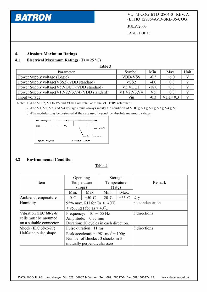
4. Absolute Maximum Ratings
4.1 Electrical Maximum Ratings (Ta = 25 ºC)
Table 3Parameter Symbol Min. Max. Unit
Power Supply voltage (Logic) VDD-VSS -0.3 +6.0 VPower Supply voltage(VSS2)(VDD standard) VSS2 -4.0 +0.3 V Power Supply voltage(V5,VOUT)(VDD standard) V5,VOUT -18.0 +0.3 V Power Supply voltage(V1,V2,V3,V4)(VDD standard) V1,V2,V3,V4 V5 +0.3 V Input voltage Vin -0.3 VDD+0.3 V
Note: 1.)The VSS2, V1 to V5 and VOUT are relative to the VDD=0V reference.
2.)The V1, V2, V3, and V4 voltages must always satisfy the condition of VDD V1 V2 V3 V4 V5.
3.)The modules may be destroyed if they are used beyond the absolute maximum ratings.
4.2 Environmental Condition
Table 4
OperatingTemperature
(Topr)
StorageTemperature
(Tstg) Item
Min. Max. Min. Max.
Remark
Ambient Temperature 0¯C +50¯C -20¯C +65¯C DryHumidity 95% max. RH for Ta ¢ 40¯C
< 95% RH for Ta > 40¯Cno condensation
Vibration (IEC 68-2-6) cells must be mounted on a suitable connector
Frequency: 10 ~ 55 Hz Amplitude: 0.75 mm Duration: 20 cycles in each direction.
3 directions
Shock (IEC 68-2-27) Half-sine pulse shape
Pulse duration : 11 ms Peak acceleration: 981 m/s2 = 100g Number of shocks : 3 shocks in 3 mutually perpendicular axes.
3 directions
www.data-modul.deDATA MODUL AG Landsberger Str. 322 80687 München Tel.: 089/ 56017-0 Fax 089/ 56017-119

VL-FS-COG-BTD12864-01 REV. A(BTHQ 128064AVD-SRE-06-COG)
JULY/2003
PAGE 12 OF 16
5. Electrical Specifications
5.1 Typical Electrical Characteristics
At Ta = +25 ¯C, VDD = +3.3°5%, VSS = 0V.
Table 5
Parameter Symbol Conditions Min. Typ. Max. Unit Supply voltage (Logic)
VDD-VSS 3.14 3.3 3.47 V
Ta = 0 ¯C,Character mode VDD = +3.3V, Note 1
- 8.80 - V
Ta = 25 ¯C,Character mode VDD = +3.3V, Note 1
8.45 8.65 8.85 V
Supply voltage (LCD) (built-in)
VLCD=VDD-V5
Ta = 50 ¯C,Character mode VDD = +3.3V, Note 1
- 7.95 - V
Low-level input signal voltage
VILC Note 2 VSS - 0.2xVDD V
High-level input signal voltage
VIHC Note 2 0.8xVDD - VDD V
VDD = +3.3V,Note 1, Character mode
- 0.3 0.45 mA Supply Current (Logic & LCD)
IDD
VDD = +3.3V,Note 1, Checker board mode
- 0.5 0.75 mA
Note 1: There is tolerance in optimum LCD driving voltage during production and it will be
within the specified range.
Note 2: A0, D0 to D5,D6(SCL),D7(SI),E(RD),R/W(WR),CS1,C86,P/S,RES terminals.
www.data-modul.deDATA MODUL AG Landsberger Str. 322 80687 München Tel.: 089/ 56017-0 Fax 089/ 56017-119
VL-FS-COG-BTD12864-01 REV. A(BTHQ 128064AVD-SRE-06-COG)
JULY/2003
PAGE 13 OF 16
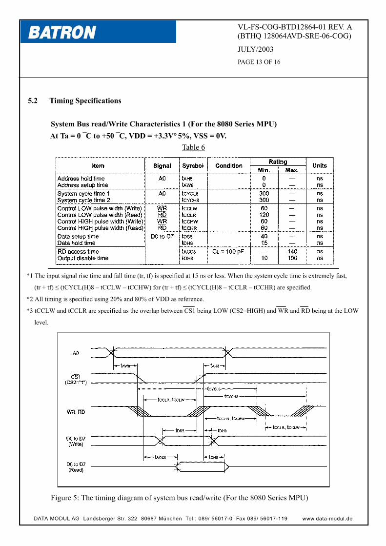
5.2 Timing Specifications
System Bus read/Write Characteristics 1 (For the 8080 Series MPU)
At Ta = 0 ¯C to +50 ¯C, VDD = +3.3V°5%, VSS = 0V.
Table 6
*1 The input signal rise time and fall time (tr, tf) is specified at 15 ns or less. When the system cycle time is extremely fast,
(tr + tf) (tCYCL(H)8 – tCCLW – tCCHW) for (tr + tf) (tCYCL(H)8 – tCCLR – tCCHR) are specified.
*2 All timing is specified using 20% and 80% of VDD as reference.
*3 tCCLW and tCCLR are specified as the overlap between CS1 being LOW (CS2=HIGH) and WR and RD being at the LOW
level.
Figure 5: The timing diagram of system bus read/write (For the 8080 Series MPU)
www.data-modul.deDATA MODUL AG Landsberger Str. 322 80687 München Tel.: 089/ 56017-0 Fax 089/ 56017-119

VL-FS-COG-BTD12864-01 REV. A(BTHQ 128064AVD-SRE-06-COG)
JULY/2003
PAGE 14 OF 16
System Bus read/Write Characteristics 2 (For the 6800 Series MPU)
At Ta = 0 ¯C to +50 ¯C, VDD = +3.3V°5%, VSS = 0V.
Table 7
*1 The input signal rise time and fall time (tr, tf) is specified at 15 ns or less. When the system cycle time is extremely fast,
(tr + tf) (tCYCH(L)6 – tEWLW – tEWHW) for (tr + tf) (tCYCH(L)6 – tEWLR – tEWHR) are specified.
*2 All timing is specified using 20% and 80% for VDD as the reference.
*3 tEWLW and tEWLR are specified as the overlap between CS1 being LOW (CS2=HIGH) and E.
Figure 6: The timing diagram of system bus read/write (For the 6800 Series MPU)
www.data-modul.deDATA MODUL AG Landsberger Str. 322 80687 München Tel.: 089/ 56017-0 Fax 089/ 56017-119
VL-FS-COG-BTD12864-01 REV. A(BTHQ 128064AVD-SRE-06-COG)
JULY/2003
PAGE 15 OF 16
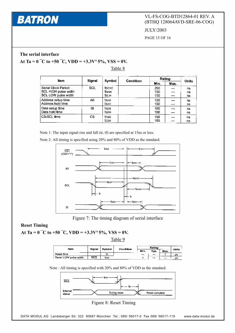
The serial interface
At Ta = 0 ¯C to +50 ¯C, VDD = +3.3V°5%, VSS = 0V.
Table 8
Note 1: The input signal rise and fall (tr, tf) are specified at 15ns or less.
Note 2: All timing is specified using 20% and 80% of VDD as the standard.
Figure 7: The timing diagram of serial interface
Reset Timing
At Ta = 0 ¯C to +50 ¯C, VDD = +3.3V°5%, VSS = 0V.
Table 9
Note : All timing is specified with 20% and 80% of VDD as the standard.
Figure 8: Reset Timing
www.data-modul.deDATA MODUL AG Landsberger Str. 322 80687 München Tel.: 089/ 56017-0 Fax 089/ 56017-119
VL-FS-COG-BTD12864-01 REV. A(BTHQ 128064AVD-SRE-06-COG)
JULY/2003
PAGE 16 OF 16
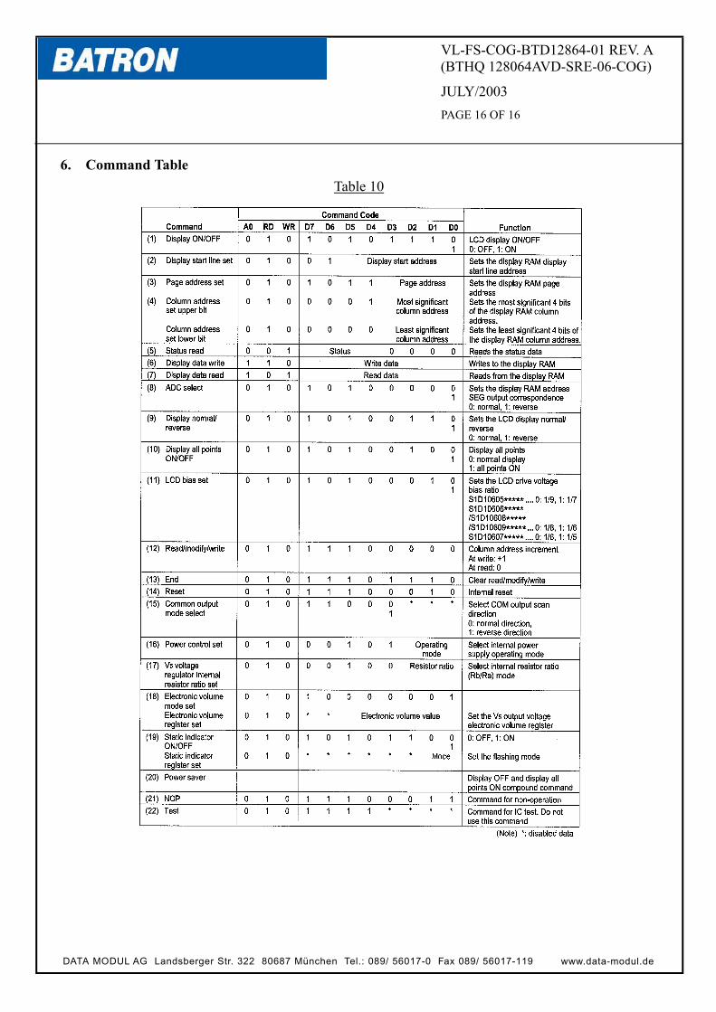
6. Command Table
Table 10
www.data-modul.deDATA MODUL AG Landsberger Str. 322 80687 München Tel.: 089/ 56017-0 Fax 089/ 56017-119