spec no. tq3c-8eaf0-e1yaf42-01 type : tcg 08 4sv … · spec no. tq3c-8eaf0-e1yaf42-01 spec d ate...
TRANSCRIPT

Spec No. TQ3C-8EAF0-E1YAF42-01
SPEC Date October 17, 2014
TYPE : TCG084SVLQAPFA-AA20
< 8.4 inch SVGA transmissive color TFT with LED backlight
constant current circuit for LED backlight and touch panel>
KYOCERA DISPLAY CORPORATION
This specification is subject to change without notice.
Consult Kyocera before ordering.
Original
Issue Date
Designed by: Engineering dept. Confirmed by: QA dept.
Prepared Checked Approved Checked Approved
January 30, 2013
CONTENTS
1. Application
2. Construction and outline
3. Mechanical specifications
4. Absolute maximum ratings
5. Electrical characteristics
6. Optical characteristics
7. Interface signals
8. Input timing characteristics
9. Design guidance for analog touch panel
10. Lot number identification
11. Warranty
12. Precautions for use
13. Reliability test data
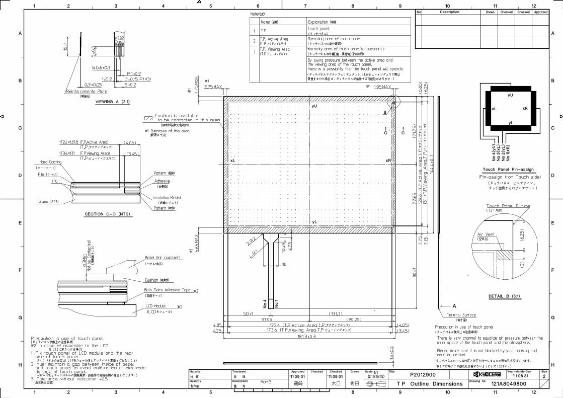
14. Outline drawing
Nov 11,2014

Spec No.
TQ3C-8EAF0-E1YAF42-01
Part No.
TCG084SVLQAPFA-AA20
Page
-
Warning
1. This Kyocera LCD module has been specifically designed for use only in
electronic devices and industrial machines in the area of audio control,
office automation, industrial control, home appliances, etc. The module
should not be used in applications where the highest level of safety and
reliability are required and module failure or malfunction of such module
results in physical harm or loss of life, as well as enormous damage or loss.
Such fields of applications include, without limitation, medical, aerospace,
communications infrastructure, atomic energy control. Kyocera expressly
disclaims any and all liability resulting in any way to the use of the module
in such applications.
2. Customer agrees to indemnify, defend and hold Kyocera harmless
from and against any and all actions, claims, damages, liabilities,
awards, costs, and expenses, including legal expenses, resulting from or
arising out of Customer's use, or sale for use, or Kyocera modules in
applications.
Caution
1. Kyocera shall have the right, which Customer hereby acknowledges, to
immediately scrap or destroy tooling for Kyocera modules for which no
Purchase Orders have been received from the Customer in a two-year period.

Spec No.
TQ3C-8EAF0-E1YAF42-01
Part No.
TCG084SVLQAPFA-AA20
Page
-
Revision record
Date Designed by : Engineering dept. Confirmed by : QA dept.
Prepared Checked Approved Checked Approved
October 17, 2014
Rev.No. Date Page Descriptions
01 Oct 17, 2014 - Change KYOCERA CORPORATION LCD DIVISION
→KYOCERA DISPLAY CORPORATION
5 5-2. Constant current circuit for LED Backlight
change Operating life time Typ70,000h →100,000h
Spec No.
TQ3C-8EAF0-E1YAF42-01
Part No.
TCG084SVLQAPFA-AA20
Page
1
M407011
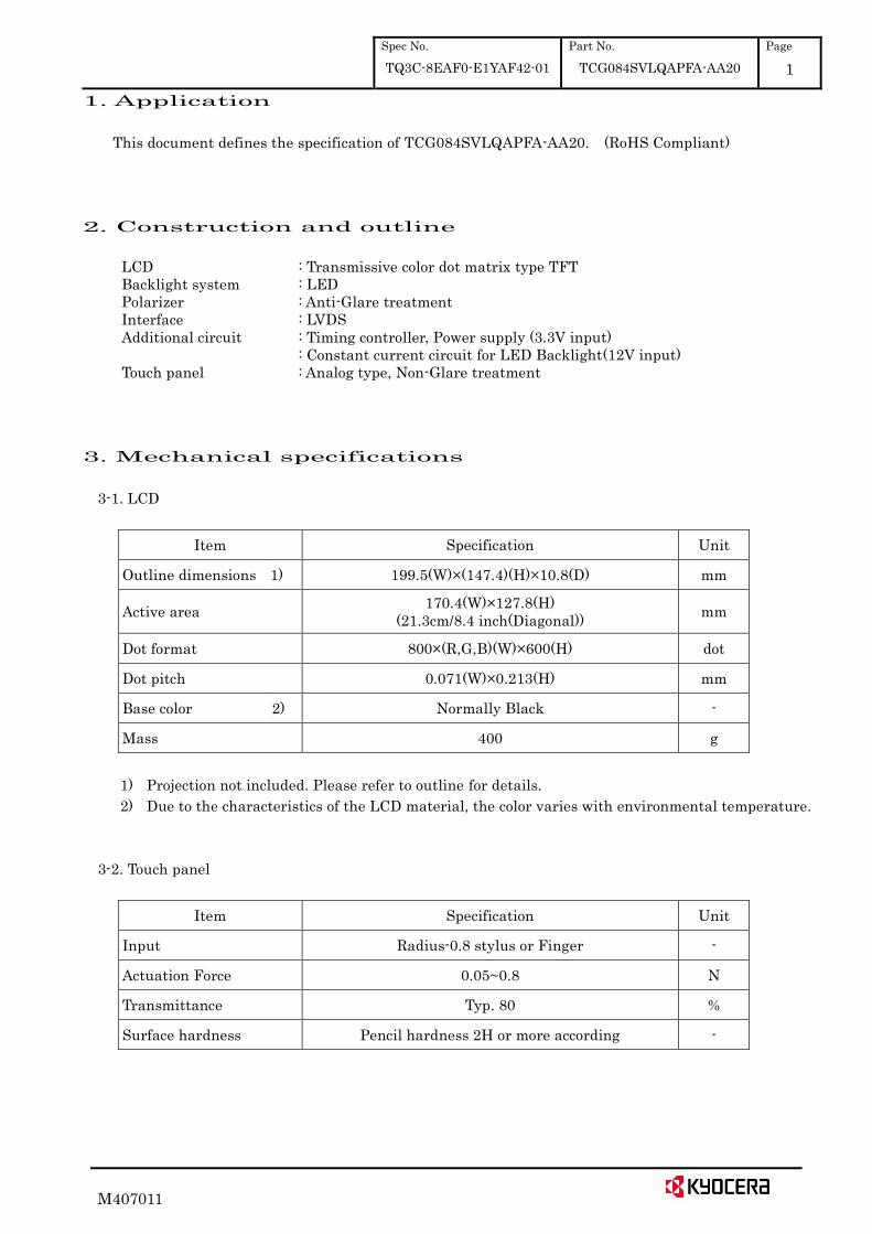
1. Application
This document defines the specification of TCG084SVLQAPFA-AA20. (RoHS Compliant)
2. Construction and outline
LCD
Backlight system
Polarizer
Interface
Additional circuit
Touch panel
: Transmissive color dot matrix type TFT
: LED
: Anti-Glare treatment
: LVDS
: Timing controller, Power supply (3.3V input)
: Constant current circuit for LED Backlight(12V input)
: Analog type, Non-Glare treatment
3. Mechanical specifications
3-1. LCD
Item Specification Unit
Outline dimensions 1) 199.5(W)×(147.4)(H)×10.8(D) mm
Active area 170.4(W)×127.8(H)
(21.3cm/8.4 inch(Diagonal)) mm
Dot format 800×(R,G,B)(W)×600(H) dot
Dot pitch 0.071(W)×0.213(H) mm
Base color 2) Normally Black -
Mass 400 g
1) Projection not included. Please refer to outline for details.
2) Due to the characteristics of the LCD material, the color varies with environmental temperature.
3-2. Touch panel
Item Specification Unit
Input Radius-0.8 stylus or Finger -
Actuation Force 0.05~0.8 N
Transmittance Typ. 80 %
Surface hardness Pencil hardness 2H or more according -

Spec No.
TQ3C-8EAF0-E1YAF42-01
Part No.
TCG084SVLQAPFA-AA20
Page
2
M407011
4. Absolute maximum ratings
4-1. Electrical absolute maximum ratings
Item Symbol Min. Max. Unit
Supply voltage(+3.3V) VDD -0.3 4.0 V
Supply voltage(+12V) VIN -0.3 14.0 V
Input signal
voltage 2)
RxINi+, RxINi- 1) VI1 -0.3 2.8 V
CK IN+, CK IN- VI2 -0.3 2.8 V
SELLVDS VI3 -0.3 VDD+0.5 V
BLBRT, BLEN VI4 -0.3 VIN V
Supply voltage for touch panel VTP 0 6.0 V
Input current of touch panel ITP 0 0.5 mA
1) i=0,1,2,3
2) VDD must be supplied correctly within the range described in 5-1.
4-2. Environmental absolute maximum ratings
Item Symbol Min. Max. Unit
Operating temperature 1) TOP -20 70 °C
Storage temperature 2) TSTO -30 80 °C
Operating humidity 3) HOP 10 4) %RH
Storage humidity 3) HSTO 10 4) %RH
Vibration - 5) 5) -
Shock - 6) 6) -
1) Operating temperature means a temperature which operation shall be guaranteed. Since display
performance is evaluated at 25°C, another temperature range should be confirmed.
2) Temp. = -30°C<48h , Temp. = 80°C<168h
Store LCD at normal temperature/humidity. Keep them free from vibration and shock.
An LCD that is kept at a low or a high temperature for a long time can be defective due to
other conditions, even if the low or high temperature satisfies the standard.
(Please refer to “Precautions for Use” for details.)
3) Non-condensing
4) Temp.≦40°C, 85%RH Max.
Temp.>40°C, Absolute humidity shall be less than 85%RH at 40°C.
5)
Frequency 10~55 Hz Acceleration value
(0.3~9 m/s2) Vibration width 0.15mm
Interval 10-55-10 Hz 1minutes
2 hours in each direction X, Y, Z (6 hours total)
EIAJ ED-2531
6) Acceleration: 490 m/s2, Pulse width: 11 ms
3 times in each direction: ±X, ±Y, ±Z
EIAJ ED-2531
Spec No.
TQ3C-8EAF0-E1YAF42-01
Part No.
TCG084SVLQAPFA-AA20
Page
3
M407011
5. Electrical characteristics
5-1. LCD
Temp. = -20~70°C
Item Symbol Condition Min. Typ. Max. Unit
Supply voltage 1) VDD - 3.0 3.3 3.6 V
Current consumption IDD 2) - 270 330 mA
Permissive input ripple voltage VRP VDD=3.3V - - 100 mVp-p
Input signal voltage 3) VIL "Low" level 0 - 0.8 V
VIH "High" level 2.0 - VDD V
Input reek current IOL VI3=0V -10 - 10 μA
IOH VI3=3.3V - - 400 μA
LVDS Input voltage 4) VL - 0 - 1.9 V
Differential input voltage 4) VID - 250 350 450 mV
Differential input
threshold voltage 4) 5)
VTL "Low" level VCM-100 - - mV
VTH "High" level - - VCM+100 mV
Terminator R1 - - 100 - Ω
VDD-turn-on conditions 1)
t1 - 0.1 - 10 ms
t2 - 0 - - ms
t3 - 0 - - ms
t4 - 1.0 - - s
t5 - 200 - - ms
t6 - 200 - - ms
t7 - 0 - 10 s
t8 - 0 - - ms
1) VDD-turn-on conditions
Spec No.
TQ3C-8EAF0-E1YAF42-01
Part No.
TCG084SVLQAPFA-AA20
Page
4
M407011
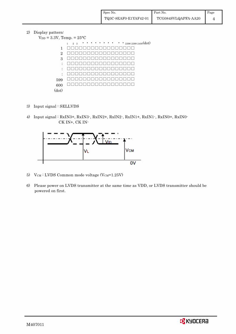
2) Display pattern:
VDD = 3.3V, Temp. = 25°C
1 2 3 ・・・・・・・・ ・・2398 2399 2400(dot)
1
2
3
:
:
:
599
600
(dot)
□□□□□□□□□□□□□□□□□
□□□□□□□□□□□□□□□□□
□□□□□□□□□□□□□□□□□
□□□□□□□□□□□□□□□□□
□□□□□□□□□□□□□□□□□
□□□□□□□□□□□□□□□□□
□□□□□□□□□□□□□□□□□
□□□□□□□□□□□□□□□□□
3) Input signal : SELLVDS
4) Input signal : RxIN3+, RxIN3-, RxIN2+, RxIN2-, RxIN1+, RxIN1-, RxIN0+, RxIN0-
CK IN+, CK IN-
5) VCM : LVDS Common mode voltage (VCM=1.25V)
6) Please power on LVDS transmitter at the same time as VDD, or LVDS transmitter should be
powered on first.

Spec No.
TQ3C-8EAF0-E1YAF42-01
Part No.
TCG084SVLQAPFA-AA20
Page
5
M407011
5-2. Constant current circuit for LED Backlight
Temp. = -20~70°C
Item Symbol Condition Min. Typ. Max. Unit
Supply voltage 1) VIN - 10.8 12.0 13.2 V
Current consumption IIN 2) - 330 500 mA
Permissive input ripple voltage VRP_BL VIN=12.0V - - 100 mVp-p
BLBRT Input signal voltage VIL_BLBRT "Low" level 0 - 0.8 V
VIH_BLBRT "High" level 2.3 - VIN V
BLBRT Input pull-down resistance RIN_BLBRT - 100 300 500 kΩ
BLEN Input signal voltage VIL_BLEN "Low" level 0 - 0.8 V
VIH_BLEN "High" level 2.3 - VIN V
BLEN Input pull-down resistance RIN_BLEN - 100 300 500 kΩ
PWM Frequency 3) fPWM - 200 - 10k Hz
PWM Duty ratio 3) DPWM
fPWM=200Hz 1 - 100 %
fPWM=2kHz 10 - 100 %
fPWM=10kHz 50 - 100 %
Operating life time 4), 5) T Temp.=25°C - 100,000 - h
1) VIN-turn-on conditions

Spec No.
TQ3C-8EAF0-E1YAF42-01
Part No.
TCG084SVLQAPFA-AA20
Page
6
M407011
2) VIN = 12V, Temp. = 25℃,DPWM = 100%
3) PWM Timing Diagram
tON,tOFF ≧ 50μs.
In case of lower frequency, the deterioration of the display quality, flicker etc., may occur.
4) When brightness decrease 50% of minimum brightness.
The average life of a LED will decrease when the LCD is operating at higher temperatures.
5) Life time is estimated data.(Condition : IF=60mA, Ta=25℃ in chamber).
5-3. Touch panel
Item Specification
Supply voltage for touch panel 5.0V
Terminal resistance xL~xR:363Ω~847Ω
yU~yL:230Ω~536Ω
Linearity less than ±2.0%
Insulation resistance 100MΩ or more at DC25V
Spec No.
TQ3C-8EAF0-E1YAF42-01
Part No.
TCG084SVLQAPFA-AA20
Page
7
M407011
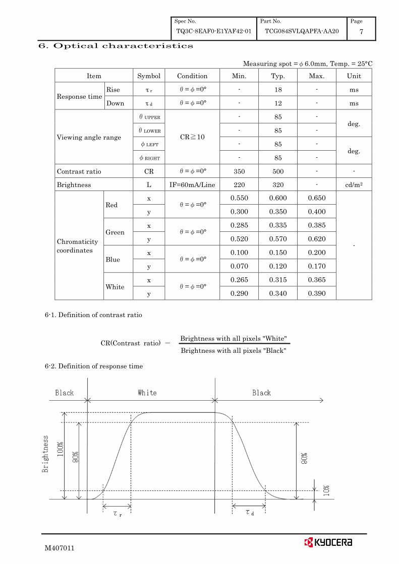
6. Optical characteristics
Measuring spot =φ6.0mm, Temp. = 25°C
Item Symbol Condition Min. Typ. Max. Unit
Response time Rise τ r θ=φ=0° - 18 - ms
Down τ d θ=φ=0° - 12 - ms
Viewing angle range
θUPPER
CR≧10
- 85 - deg.
θLOWER - 85 -
φLEFT - 85 - deg.
φRIGHT - 85 -
Contrast ratio CR θ=φ=0° 350 500 - -
Brightness L IF=60mA/Line 220 320 - cd/m2
Chromaticity
coordinates
Red x
θ=φ=0° 0.550 0.600 0.650
-
y 0.300 0.350 0.400
Green x
θ=φ=0° 0.285 0.335 0.385
y 0.520 0.570 0.620
Blue x
θ=φ=0° 0.100 0.150 0.200
y 0.070 0.120 0.170
White x
θ=φ=0° 0.265 0.315 0.365
y 0.290 0.340 0.390
6-1. Definition of contrast ratio
CR(Contrast ratio) =
Brightness with all pixels "White"
Brightness with all pixels "Black"
6-2. Definition of response time
Spec No.
TQ3C-8EAF0-E1YAF42-01
Part No.
TCG084SVLQAPFA-AA20
Page
8
M407011
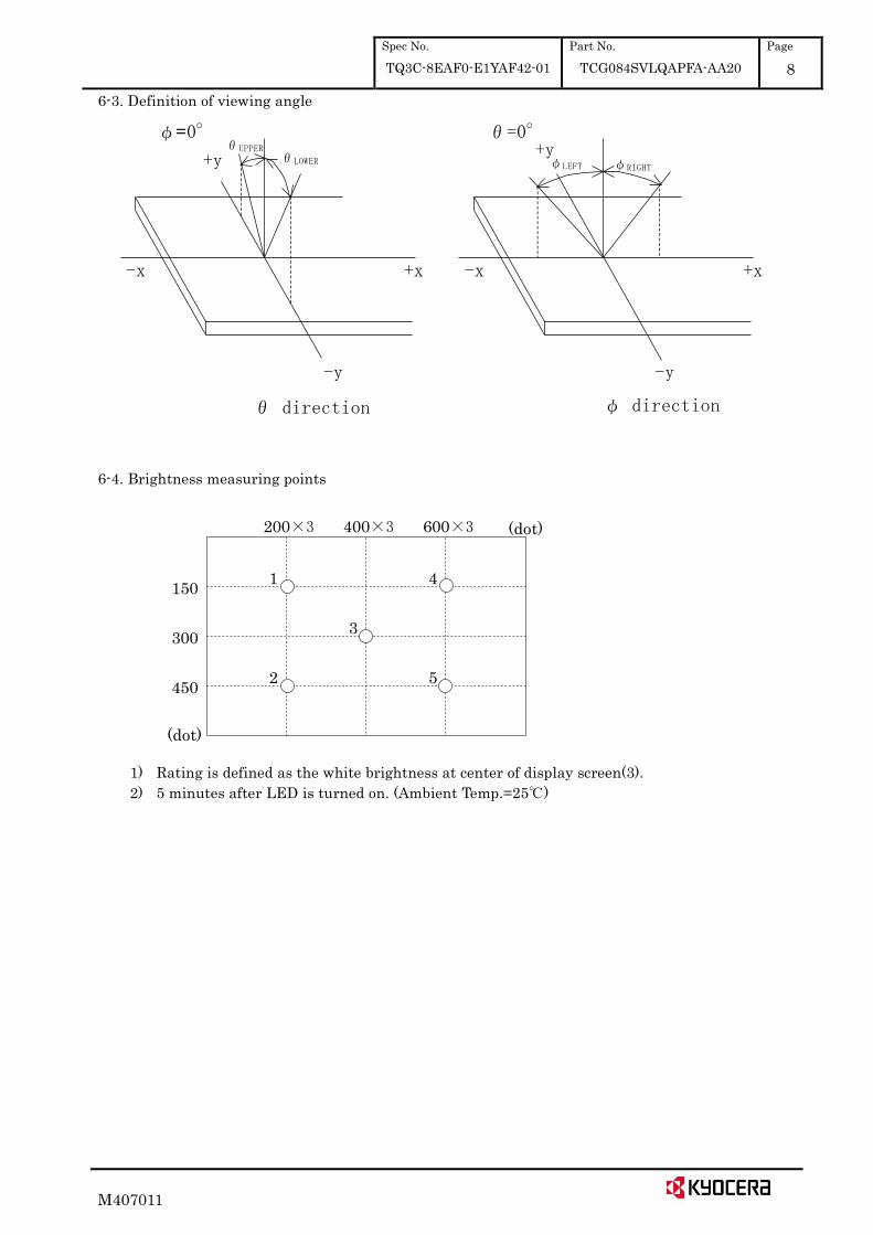
6-3. Definition of viewing angle
6-4. Brightness measuring points
1) Rating is defined as the white brightness at center of display screen(3).
2) 5 minutes after LED is turned on. (Ambient Temp.=25℃)
-x +x
-y
+y
φ=0°
θLOWER
θUPPER
-x +x
-y
θ=0°
φRIGHTφLEFT
θ direction φ direction
+y
(dot)
(dot)200×3 400×3 600×3
150
300
450
1
2
3
4
5

Spec No.
TQ3C-8EAF0-E1YAF42-01
Part No.
TCG084SVLQAPFA-AA20
Page
9
M407011
7. Interface signals
7-1. Interface signals
No. Symbol Description Note
1 GND GND
2 SELLVDS Mode select signal(LVDS Data mapping)
3 GND GND
4 GND GND
5 RxIN3+ LVDS receiver signal CH3(+) LVDS
6 RxIN3- LVDS receiver signal CH3(-) LVDS
7 GND GND
8 CK IN+ LVDS receiver signal CK(+) LVDS
9 CK IN- LVDS receiver signal CK(-) LVDS
10 GND GND
11 RxIN2+ LVDS receiver signal CH2(+) LVDS
12 RxIN2- LVDS receiver signal CH2(-) LVDS
13 GND GND
14 RxIN1+ LVDS receiver signal CH1(+) LVDS
15 RxIN1- LVDS receiver signal CH1(-) LVDS
16 GND GND
17 RxIN0+ LVDS receiver signal CH0(+) LVDS
18 RxIN0- LVDS receiver signal CH0(-) LVDS
19 GND GND
20 GND GND
21 VDD +3.3V power supply
22 VDD +3.3V power supply
23 GND GND
24 BLBRT PWM signal(Brightness adjustment)
25 BLEN ON/OFF terminal voltage
26 GND GND
27 VIN +12V power supply
28 VIN +12V power supply
29 GND GND
30 GND GND
LCD connector : FI-X30SSLA-HF (JAE)
Matching connector : FI-X30HL (JAE)
: FI-X30HL-T (JAE)
: FI-X30C2L-NPB (JAE)
: FI-X30C2L-T-NPB (JAE)
LVDS receiver : Embedded in ASIC
Matching LVDS transmitter : THC63LVDM83R(THine Electronics) or compatible

Spec No.
TQ3C-8EAF0-E1YAF42-01
Part No.
TCG084SVLQAPFA-AA20
Page
10
M407011
7-2. Data mapping(6bit RGB input)
1) Location of SELLVDS (THC63LVDM83R(THine Electronics) or compatible)
Transmitter 2Pin SELLVDS
Pin No. Data = L(GND) or OPEN = H(3.3V)
51 TA0 - R0(LSB)
52 TA1 - R1
54 TA2 - R2
55 TA3 - R3
56 TA4 - R4
3 TA5 - R5(MSB)
4 TA6 - G0(LSB)
6 TB0 - G1
7 TB1 - G2
11 TB2 - G3
12 TB3 - G4
14 TB4 - G5(MSB)
15 TB5 - B0(LSB)
19 TB6 - B1
20 TC0 - B2
22 TC1 - B3
23 TC2 - B4
24 TC3 - B5(MSB)
27 TC4 - (HS)
28 TC5 - (VS)
30 TC6 - DE
50 TD0 - GND
2 TD1 - GND
8 TD2 - GND
10 TD3 - GND
16 TD4 - GND
18 TD5 - GND
25 TD6 - GND
SELLVDS=H(3.3V)
1 C Y C L E
DE( H S ) B5 B4 B3 B2
G2
B2 DE ( V S )
G1 B1 B0 G1 B1
R4R5 R1 R0 G0
G5 G4 G3
G0R1 R3 R2
DE:DATA ENABLE
HS:HSYNC
VS:VSYNC

Spec No.
TQ3C-8EAF0-E1YAF42-01
Part No.
TCG084SVLQAPFA-AA20
Page
11
M407011
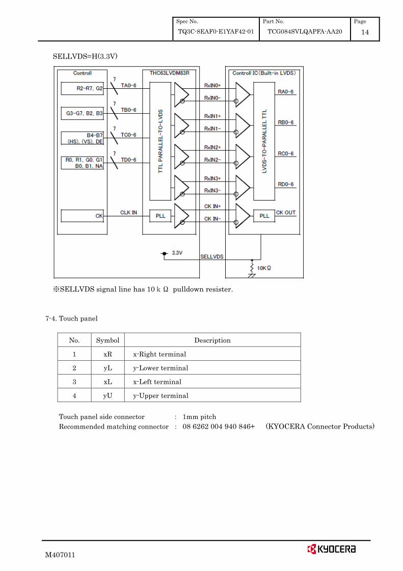
2) Block Diagram
SELLVDS=H(3.3V)
※SELLVDS signal line has 10kΩ pulldown resister.
When using “6-bit Transmitter”, please connect the unused channel of the control IC receiver
as described in the diagram below.
※SELLVDS signal line has 10kΩ pulldown resister.

Spec No.
TQ3C-8EAF0-E1YAF42-01
Part No.
TCG084SVLQAPFA-AA20
Page
12
M407011
7-3. Data mapping(8bit RGB input)
1) Location of SELLVDS (THC63LVDM83R(THine Electronics) or compatible)
Transmitter 2Pin SELLVDS
Pin No. Data = L(GND) or OPEN = H(3.3V)
51 TA0 R0(LSB) R2
52 TA1 R1 R3
54 TA2 R2 R4
55 TA3 R3 R5
56 TA4 R4 R6
3 TA5 R5 R7(MSB)
4 TA6 G0(LSB) G2
6 TB0 G1 G3
7 TB1 G2 G4
11 TB2 G3 G5
12 TB3 G4 G6
14 TB4 G5 G7(MSB)
15 TB5 B0(LSB) B2
19 TB6 B1 B3
20 TC0 B2 B4
22 TC1 B3 B5
23 TC2 B4 B6
24 TC3 B5 B7(MSB)
27 TC4 (HS) (HS)
28 TC5 (VS) (VS)
30 TC6 DE DE
50 TD0 R6 R0(LSB)
2 TD1 R7(MSB) R1
8 TD2 G6 G0(LSB)
10 TD3 G7(MSB) G1
16 TD4 B6 B0(LSB)
18 TD5 B7(MSB) B1
25 TD6 (NA) (NA)
SELLVDS=L(GND) or OPEN
1 CYCLE
NA
R1
G2
B3
R7 G7 G6 R7 R6R6 NA B7 B6
DE(HS) B5 B4 B3 B2
G2
B2 DE (VS)
G1 B1 B0 G1 B1
R4R5 R1 R0 G0
G5 G4 G3
G0R0 R3 R2
DE:DATA ENABLE
HS:HSYNC
VS:VSYNC

Spec No.
TQ3C-8EAF0-E1YAF42-01
Part No.
TCG084SVLQAPFA-AA20
Page
13
M407011
SELLVDS=H(3.3V)
1 C Y C L E
R0 G1 G0 R1 R0
R3
G4
B5
R1 NA B1 B0
DE( H S ) B7 B6 B5 B4
NA
G4
B4 DE ( V S )
G3 B3 B2 G3 B3
R6R7 R3 R2 G2
G7 G6 G5
G2R2 R5 R4
DE:DATA ENABLE
HS:HSYNC
VS:VSYNC
2) Block Diagram
SELLVDS=L(GND) or OPEN
※SELLVDS signal line has 10kΩ pulldown resister.
Spec No.
TQ3C-8EAF0-E1YAF42-01
Part No.
TCG084SVLQAPFA-AA20
Page
14
M407011
SELLVDS=H(3.3V)
※SELLVDS signal line has 10kΩ pulldown resister.
7-4. Touch panel
No. Symbol Description
1 xR x-Right terminal
2 yL y-Lower terminal
3 xL x-Left terminal
4 yU y-Upper terminal
Touch panel side connector : 1mm pitch
Recommended matching connector : 08 6262 004 940 846+ (KYOCERA Connector Products)

Spec No.
TQ3C-8EAF0-E1YAF42-01
Part No.
TCG084SVLQAPFA-AA20
Page
15
M407011
8. Input timing characteristics
8-1. Timing characteristics
Item Symbol Min. Typ. Max. Unit Note
Clock (CK) Frequency 1/Tc 30 40 48 MHz
Enable signal
(DE)
Horizontal Period Th 860 1056 1395 Tc
24.0 26.4 - μs 1)
Horizontal display period Thd 800 Tc
Vertical Period Tv 610 628 1024 Th
Vertical display period Tvd 600 Th
Refresh rate fv 50 60 70 Hz 2)
1) Please set a clock frequency, a vertical dormant period, and the horizontal dormant period
so that the Horizontal Period should not reach less than Min. value.
2) If the refresh rate reach less than Min. value, the deterioration of the display quality, flicker etc.,
may occur.(fv=1/Tv) Vertical Timing Diagram
Data DH1 DH2 DH3 DH598 DH599 DH600 DH1
DE
Tvd
Tv
Horizontal Timing Diagram
Tc
CK
Data D1 D2 D3 D798 D799 D800 D1
DE
Thd
Th
8-2. Input Data Signals and Display position on the screen
D 1 , D H 1D 2 , D H 1D 3 , D H 1 D 8 0 0 , D H 1
G B
D 1 , D H 6 0 0D 2 , D H 6 0 0D 3 , D H 6 0 0
D 1 , D H 2D 2 , D H 2D 3 , D H 2
R

Spec No.
TQ3C-8EAF0-E1YAF42-01
Part No.
TCG084SVLQAPFA-AA20
Page
16
M407011
9. Design guidance for analog touch panel
9-1. Electrical (In customer's design, please remember the following considerations.)
1) Do not use the current regulated circuit.
2) Keep the current limit with top and bottom layer.
(Please refer to “Electrical absolute maximum ratings” for details.)
3) Analog touch panel can not sense two points touching separately.
4) A contact resistance is appeared at the touch point between top and bottom layer.
After this resistance has stable read of the touch panel position data.
5) Because noise of inverter or peripheral circuits may interfere signal of touch panel itself
it is necessary to design carefully in advance to avoid these noise problem.
9-2. Software
1) Do the "User Calibration".
2) "User Calibration" may be needed with long term using.
Include "User Calibration" menu in your software.
3) When drawing a line with a stylus, there may be a slight discontinuity when the stylus
passes over a spacer-dot. If necessary, please provide a compensation feature within your
software.
9-3. Mounting on display and housing bezel
1) Do not use an adhesive tape to bond it on the front of touch panel and hang it to the housing
bezel.
2) Never expand the touch panel top layer (PET-film) like a balloon by internal air pressure.
The life of the touch panel will be extremely short.
3) If a dew will be on the heat-sealed area or exposed traces at the end of a flexible tail,
the migration of silver can occur. This will cause sometimes a short circuit.
4) Must maintain a gap between inside of bezel and touch panel to avoid malfunction or electrode
damage of touch panel.
Spec No.
TQ3C-8EAF0-E1YAF42-01
Part No.
TCG084SVLQAPFA-AA20
Page
17
M407011
10. Lot number identification
The lot number shall be indicated on the back of the backlight case of each LCD.
TCG084SVLQAPFA-AA20 - □□ - □□ - □ MADE IN □□□□□
↓ ↓ ↓ ↓ ↓
1 2 3 4 5
Year 2013 2014 2015 2016 2017 2018
Code 3 4 5 6 7 8
Month Jan. Feb. Mar. Apr. May Jun.
Code 1 2 3 4 5 6
Month Jul. Aug. Sep. Oct. Nov. Dec.
Code 7 8 9 X Y Z
11. Warranty
11-1. Incoming inspection
Please inspect the LCD within one month after your receipt.
11-2. Production warranty
Kyocera warrants its LCD’s for a period of 12 months from the ship date. Kyocera shall, by mutual
agreement, replace or re-work defective LCD’s that are shown to be Kyocera’s responsibility.
No1. - No5. above indicate
1. Year code
2. Month code
3. Date
4. Version Number
5. Country of origin (Japan or China)
Spec No.
TQ3C-8EAF0-E1YAF42-01
Part No.
TCG084SVLQAPFA-AA20
Page
18
M407011
12. Precautions for use
12-1. Installation of the LCD
1) Please ground either of the mounting (screw) holes located at each corner of an LCD,
in order to stabilize brightness and display quality.
2) The LCD shall be installed so that there is no pressure on the LSI chips.
3) Since this product is wide viewing product, occurrence level of in-plane unevenness by the external stress is different compared to current normal viewing product. So there is a possibility that
in-plane unevenness will be occurred by over twist, strain giving by attaching to LCD, and over pressure to touch panel. Please be careful of stress when designing the housing.
12-2. Static electricity 1) Workers should use body grounding. Operator should wear ground straps.
12-3. LCD operation
1) The LCD shall be operated within the limits specified. Operation at values outside of these limits
may shorten life, and/or harm display images.
2) Please select the best display pattern based on your evaluation because flicker, lines or
nonuniformity or unevenness can be visible depending on display patterns.
12-4. Storage
1) The LCD shall be stored within the temperature and humidity limits specified.
Store in a dark area, and protect the LCD from direct sunlight or fluorescent light.
2) Always store the LCD so that it is free from external pressure onto it.
12-5. Usage
1) DO NOT store in a high humidity environment for extended periods. Polarizer degradation bubbles,
and/or peeling off of the polarizer may result.
2) Do not push or rub the touch panel's surface with hard to sharp objects such as knives, or
the touch panel may be scratched.
3) When the touch panel is dirty, gently wipe the surface with a soft cloth, sometimes
moistened by mild detergent or alcohol. If a hazardous chemical is dropped on the touch
panel by mistake, wipe it off right away to prevent human contact.
4) Touch panel edges are sharp. Handle the touch panel with enough care to prevent cuts.
5) Always keep the LCD free from condensation during testing. Condensation may permanently spot
or stain the polarizer.
6) Do not disassemble LCD because it will result in damage.
7) This Kyocera LCD has been specifically designed for use in general electronic devices, but not
for use in a special environment such as usage in an active gas. Hence, when the LCD is supposed
to be used in a special environment, evaluate the LCD thoroughly beforehand and do not expose
the LCD to chemicals such as an active gas.
8) Please do not use solid-base image pattern for long hours because a temporary afterimage may
appear. We recommend using screen saver etc. in cases where a solid-base image pattern must
be used.
9) Liquid crystal may leak when the LCD is broken. Be careful not to let the fluid go into your eyes
and mouth. In the case the fluid touches your body; rinse it off right away with water and soap.

Spec No.
TQ3C-8EAF0-E1YAF42-01
Part No.
TCG084SVLQAPFA-AA20
Page
19
M407011
13. Reliability test data
Test item Test condition Test time Judgement
High temp.
atmosphere 80°C 240h
Display function
Display quality
Current consumption
: No defect
: No defect
: No defect
Low temp.
atmosphere -30°C 240h
Display function
Display quality
Current consumption
: No defect
: No defect
: No defect
High temp.
humidity
atmosphere
40°C 90% RH 240h
Display function
Display quality
Current consumption
: No defect
: No defect
: No defect
Temp. cycle
-30°C
R.T.
80°C
0.5h
0.5h
0.5h
10cycles
Display function
Display quality
Current consumption
: No defect
: No defect
: No defect
High temp.
operation 70°C 500h
Display function
Display quality
Current consumption
: No defect
: No defect
: No defect
Point
Activation
life
Silicon rubber,
Tip : R = 4.0
Hitting force 3N
Hitting speed
2 time/s
one
million
times
Terminal resistance
Insulation resistance
Linearity
Actuation Force
: No defect
: No defect
: No defect
: No defect
1) Each test item uses a test LCD only once. The tested LCD is not used in any other tests.
2) The LCD is tested in circumstances in which there is no condensation.
3) The reliability test is not an out-going inspection.
4) The result of the reliability test is for your reference purpose only.
The reliability test is conducted only to examine the LCD's capability.


Spec No. TQ3C-8EAF0-E2YAF42-01
Date October 17, 2014
KYOCERA INSPECTION STANDARD
TYPE : TCG084SVLQAPFA-AA20
KYOCERA DISPLAY CORPORATION
Original
Issue Date
Designed by : Engineering dept. Confirmed by : QA dept.
Prepared Checked Approved Checked Approved
January 30, 2013

Spec No.
TQ3C-8EAF0-E2YAF42-01
Part No.
TCG084SVLQAPFA-AA20
Page
-
Revision record
Date Designed by : Engineering dept. Confirmed by : QA dept.
Prepared Checked Approved Checked Approved
October 17, 2014
Rev.No. Date Page Descriptions
01 Oct 17, 2014 - Change KYOCERA CORPORATION LCD DIVISION
→KYOCERA DISPLAY CORPORATION
1 Change “Definition of inspection item”, Bright dot defect
Spec No.
TQ3C-8EAF0-E2YAF42-01
Part No.
TCG084SVLQAPFA-AA20
Page
1
Visuals specification
1) Note
Note
General 1. Customer identified anomalies not defined within this inspection standard shall be
reviewed by Kyocera, and an additional standard shall be determined by mutual consent.
2. This inspection standard about the image quality shall be applied to any defect within the
effective viewing area and shall not be applicable to outside of the area.
3. Inspection conditions
Luminance
Inspection distance
Temperature
Direction
: 500 Lux min.
: 300 mm.
: 25 ± 5℃
: Directly above
Definition of
inspection
item
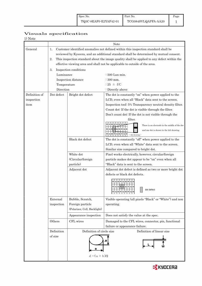
Dot defect Bright dot defect The dot is constantly “on” when power applied to the
LCD, even when all “Black” data sent to the screen.
Inspection tool: 5% Transparency neutral density filter.
Count dot: If the dot is visible through the filter.
Don’t count dot: If the dot is not visible through the
filter.
R G B R G B R G B
R G B R G B R G B
R G B R G B R G B
Black dot defect
The dot is constantly “off” when power applied to the
LCD, even when all “White” data sent to the screen.
Similar size compared to bright dot.
White dot
(Circular/foreign
particle)
Pixel works electrically, however, circular/foreign
particle makes dot appear to be “on” even when all
“Black” data is sent to the screen.
Adjacent dot Adjacent dot defect is defined as two or more bright dot
defects or black dot defects.
R G B R G B R G B
R G B R G B R G B
R G B R G B R G B
dot defect
External
inspection
Bubble, Scratch,
Foreign particle
(Polarizer, Cell, Backlight)
Visible operating (all pixels “Black” or “White”) and non
operating.
Appearance inspection Does not satisfy the value at the spec.
Others CFL wires Damaged to the CFL wires, connector, pin, functional
failure or appearance failure.
Definition
of size
Definition of circle size
d=(a+b)/2
Definition of linear size
<dot drawing>
There is an electrode in the middle of the dot
and one dot is shown in the left drawing.
Spec No.
TQ3C-8EAF0-E2YAF42-01
Part No.
TCG084SVLQAPFA-AA20
Page
2
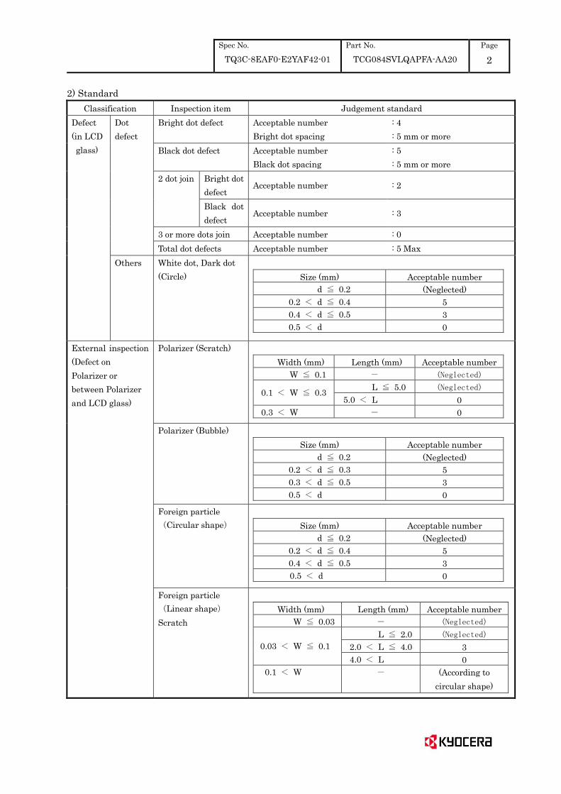
2) Standard
Classification Inspection item Judgement standard
Defect
(in LCD
glass)
Dot
defect
Bright dot defect Acceptable number
Bright dot spacing
: 4
: 5 mm or more
Black dot defect Acceptable number
Black dot spacing
: 5
: 5 mm or more
2 dot join Bright dot
defect Acceptable number : 2
Black dot
defect Acceptable number : 3
3 or more dots join Acceptable number : 0
Total dot defects Acceptable number : 5 Max
Others White dot, Dark dot
(Circle)
Size (mm) Acceptable number
0.2 < d ≦ 0.2 (Neglected)
0.2 < d ≦ 0.4 5
0.4 < d ≦ 0.5 3
0.5 < d ≦ 0.4 0
External inspection
(Defect on
Polarizer or
between Polarizer
and LCD glass)
Polarizer (Scratch)
Width (mm) Length (mm) Acceptable number
0.1 < W ≦ 0.1 - (Neglected)
0.1 < W ≦ 0.3 2.0 < L ≦ 5.0 (Neglected)
5.0 < L ≦ 5.0 0
0.3 < W ≦ 0.3 - 0
Polarizer (Bubble)
Size (mm) Acceptable number
0.2 < d ≦ 0.2 (Neglected)
0.2 < d ≦ 0.3 5
0.3 < d ≦ 0.5 3
0.5 < d ≦ 0.4 0
Foreign particle
(Circular shape)
Size (mm) Acceptable number
0.2 < d ≦ 0.2 (Neglected)
0.2 < d ≦ 0.4 5
0.4 < d ≦ 0.5 3
0.5 < d ≦0 .4 0
Foreign particle
(Linear shape)
Scratch
Width (mm) Length (mm) Acceptable number
0.00 < W ≦ 0.03 - (Neglected)
0.03 < W ≦ 0.10
2.0 < L ≦ 2.0 (Neglected)
2.0 < L ≦ 4.0 3
4.0 < L ≦ 5.0 0
0.1 < W ≦0.3 - (According to
circular shape)

Spec No.
TQ3C-8EAF0-E2YAF42-01
Part No.
TCG084SVLQAPFA-AA20
Page
3
Inspection item Judgement standard
Scratch,
Foreign particle
(Touch screen
portion)
( W = Width, L = Length, D = Diameter = (major axis+minor axis)/ 2)
Item Width(mm) Length(mm) Acceptable number
Scratch
d ≦ 0.03 L ≦ 20 Neglected
0.03 < d ≦ 0.05 L ≦ 10 2pcs within φ20mm
0.05 < d ≦ 0.08 L ≦ 6 2pcs within φ20mm
0.08 < d ≦ 0.1 L ≦ 4 1pcs within φ30mm
Foreign
(line like)
W ≦ 0.05 Neglected Neglected
0.05 < W ≦ 0.1 L ≦ 5 2pcs within φ30mm
Foreign
(circle like)
D ≦ 0.2 Neglected
0.2 < D ≦ 0.3 2pcs within φ30mm
Above are applied to the visible area.
Unless there are foreign particle and damage affected seriously to the electrical
performance out of the active area, we approve of this product.
Glass crack
(Touch screen
portion) Item Size (mm)
Acceptable
number
Corner crack
X ≦3
2 pcs
/panel Y ≦3
Z <t
Crack in
other area
than in
corner
X ≦5
2 pcs
/side Y ≦1.5
Z <t
Progressive
crack
0 pcs
(NG even 1pcs)