spartan-3 pci express - digi-key sheets/xilinx pdfs/sparten-3 pci... · spartan-3 pci express...
TRANSCRIPT

R
Spartan-3PCI Express
Starter Kit BoardUser Guide v1.2
UG2565 July 21, 2006
www.xilinx.com Spartan-3 PCI Express Starter Board Kit v1.2UG2565 July 21, 2006
Xilinx is disclosing this Document and Intellectual Property (hereinafter “the Design”) to you for use in the development of designs to operate on, or interface with Xilinx FPGAs. Except as stated herein, none of the Design may be copied, reproduced, distributed, republished, downloaded, displayed, posted, or transmitted in any form or by any means including, but not limited to, electronic, mechanical, photocopying, recording, or otherwise, without the prior written consent of Xilinx. Any unauthorized use of the Design may violate copyright laws, trademark laws, the laws of privacy and publicity, and communications regulations and statutes.
Xilinx does not assume any liability arising out of the application or use of the Design; nor does Xilinx convey any license under its patents, copyrights, or any rights of others. You are responsible for obtaining any rights you may require for your use or implementation of the Design. Xilinx reserves the right to make changes, at any time, to the Design as deemed desirable in the sole discretion of Xilinx. Xilinx assumes no obligation to correct any errors contained herein or to advise you of any correction if such be made. Xilinx will not assume any liability for the accuracy or correctness of any engineering or technical support or assistance provided to you in connection with the Design.
THE DESIGN IS PROVIDED “AS IS” WITH ALL FAULTS, AND THE ENTIRE RISK AS TO ITS FUNCTION AND IMPLEMENTATION IS WITH YOU. YOU ACKNOWLEDGE AND AGREE THAT YOU HAVE NOT RELIED ON ANY ORAL OR WRITTEN INFORMATION OR ADVICE, WHETHER GIVEN BY XILINX, OR ITS AGENTS OR EMPLOYEES. XILINX MAKES NO OTHER WARRANTIES, WHETHER EXPRESS, IMPLIED, OR STATUTORY, REGARDING THE DESIGN, INCLUDING ANY WARRANTIES OF MERCHANTABILITY, FITNESS FOR A PARTICULAR PURPOSE, TITLE, AND NONINFRINGEMENT OF THIRD-PARTY RIGHTS.
IN NO EVENT WILL XILINX BE LIABLE FOR ANY CONSEQUENTIAL, INDIRECT, EXEMPLARY, SPECIAL, OR INCIDENTAL DAMAGES, INCLUDING ANY LOST DATA AND LOST PROFITS, ARISING FROM OR RELATING TO YOUR USE OF THE DESIGN, EVEN IF YOU HAVE BEEN ADVISED OF THE POSSIBILITY OF SUCH DAMAGES. THE TOTAL CUMULATIVE LIABILITY OF XILINX IN CONNECTION WITH YOUR USE OF THE DESIGN, WHETHER IN CONTRACT OR TORT OR OTHERWISE, WILL IN NO EVENT EXCEED THE AMOUNT OF FEES PAID BY YOU TO XILINX HEREUNDER FOR USE OF THE DESIGN. YOU ACKNOWLEDGE THAT THE FEES, IF ANY, REFLECT THE ALLOCATION OF RISK SET FORTH IN THIS AGREEMENT AND THAT XILINX WOULD NOT MAKE AVAILABLE THE DESIGN TO YOU WITHOUT THESE LIMITATIONS OF LIABILITY.
The Design is not designed or intended for use in the development of on-line control equipment in hazardous environments requiring fail-safe controls, such as in the operation of nuclear facilities, aircraft navigation or communications systems, air traffic control, life support, or weapons systems (“High-Risk Applications”). Xilinx specifically disclaims any express or implied warranties of fitness for such High-Risk Applications. You represent that use of the Design in such High-Risk Applications is fully at your risk.
© 2006 Xilinx, Inc. All rights reserved. XILINX, the Xilinx logo, and other designated brands included herein are trademarks of Xilinx, Inc. All other trademarks are the property of their respective owners.
[
Revision HistoryThe following table shows the revision history for this document.
Date Version Revision
May 8, 2006 1.1 Initial Xilinx release
July 21, 2006 1.2 Minor editorial updates
R
Spartan-3 PCI Express Starter Board Kit v1.2 www.xilinx.comUG2565 July 21, 2006
Preface: About This GuideAcknowledgements . . . . . . . . . . . . . . . . . . . . . . . . . . . . . . . . . . . . . . . . . . . . . . . . . . . . . . . . . . 7Contents . . . . . . . . . . . . . . . . . . . . . . . . . . . . . . . . . . . . . . . . . . . . . . . . . . . . . . . . . . . . . . . . . . . . . 7Additional Resources . . . . . . . . . . . . . . . . . . . . . . . . . . . . . . . . . . . . . . . . . . . . . . . . . . . . . . . . 8Conventions . . . . . . . . . . . . . . . . . . . . . . . . . . . . . . . . . . . . . . . . . . . . . . . . . . . . . . . . . . . . . . . . . 9
Chapter 1: IntroductionKey Components and Features . . . . . . . . . . . . . . . . . . . . . . . . . . . . . . . . . . . . . . . . . . . . . . 11The PCI Express Evaluation Core . . . . . . . . . . . . . . . . . . . . . . . . . . . . . . . . . . . . . . . . . . . . 13Technical Support. . . . . . . . . . . . . . . . . . . . . . . . . . . . . . . . . . . . . . . . . . . . . . . . . . . . . . . . . . . 13
Chapter 2: PCI Express InterfaceOverview . . . . . . . . . . . . . . . . . . . . . . . . . . . . . . . . . . . . . . . . . . . . . . . . . . . . . . . . . . . . . . . . . . . 15Operation . . . . . . . . . . . . . . . . . . . . . . . . . . . . . . . . . . . . . . . . . . . . . . . . . . . . . . . . . . . . . . . . . . . 16Connections. . . . . . . . . . . . . . . . . . . . . . . . . . . . . . . . . . . . . . . . . . . . . . . . . . . . . . . . . . . . . . . . . 16Related Resources . . . . . . . . . . . . . . . . . . . . . . . . . . . . . . . . . . . . . . . . . . . . . . . . . . . . . . . . . . . 17
Chapter 3: EXP Expansion ConnectorsOverview . . . . . . . . . . . . . . . . . . . . . . . . . . . . . . . . . . . . . . . . . . . . . . . . . . . . . . . . . . . . . . . . . . . 19Operation . . . . . . . . . . . . . . . . . . . . . . . . . . . . . . . . . . . . . . . . . . . . . . . . . . . . . . . . . . . . . . . . . . . 19Connections. . . . . . . . . . . . . . . . . . . . . . . . . . . . . . . . . . . . . . . . . . . . . . . . . . . . . . . . . . . . . . . . . 20
Chapter 4: Clock SourcesOverview . . . . . . . . . . . . . . . . . . . . . . . . . . . . . . . . . . . . . . . . . . . . . . . . . . . . . . . . . . . . . . . . . . . 25Operation . . . . . . . . . . . . . . . . . . . . . . . . . . . . . . . . . . . . . . . . . . . . . . . . . . . . . . . . . . . . . . . . . . . 25Connections. . . . . . . . . . . . . . . . . . . . . . . . . . . . . . . . . . . . . . . . . . . . . . . . . . . . . . . . . . . . . . . . . 25
Chapter 5: Switches and ButtonsOverview . . . . . . . . . . . . . . . . . . . . . . . . . . . . . . . . . . . . . . . . . . . . . . . . . . . . . . . . . . . . . . . . . . . 27Connections. . . . . . . . . . . . . . . . . . . . . . . . . . . . . . . . . . . . . . . . . . . . . . . . . . . . . . . . . . . . . . . . . 27
Chapter 6: LEDsOverview . . . . . . . . . . . . . . . . . . . . . . . . . . . . . . . . . . . . . . . . . . . . . . . . . . . . . . . . . . . . . . . . . . . 29Operation . . . . . . . . . . . . . . . . . . . . . . . . . . . . . . . . . . . . . . . . . . . . . . . . . . . . . . . . . . . . . . . . . . . 29Connections. . . . . . . . . . . . . . . . . . . . . . . . . . . . . . . . . . . . . . . . . . . . . . . . . . . . . . . . . . . . . . . . . 29
Chapter 7: VGA Display PortOverview . . . . . . . . . . . . . . . . . . . . . . . . . . . . . . . . . . . . . . . . . . . . . . . . . . . . . . . . . . . . . . . . . . . 31
Table of Contents

Spartan-3 PCI Express Starter Board Kit v1.2 www.xilinx.comUG2565 July 21, 2006
Operation . . . . . . . . . . . . . . . . . . . . . . . . . . . . . . . . . . . . . . . . . . . . . . . . . . . . . . . . . . . . . . . . . . . 31Connections. . . . . . . . . . . . . . . . . . . . . . . . . . . . . . . . . . . . . . . . . . . . . . . . . . . . . . . . . . . . . . . . . 32
Chapter 8: RS-232 PORTOverview . . . . . . . . . . . . . . . . . . . . . . . . . . . . . . . . . . . . . . . . . . . . . . . . . . . . . . . . . . . . . . . . . . . 33Operation . . . . . . . . . . . . . . . . . . . . . . . . . . . . . . . . . . . . . . . . . . . . . . . . . . . . . . . . . . . . . . . . . . . 33Connections. . . . . . . . . . . . . . . . . . . . . . . . . . . . . . . . . . . . . . . . . . . . . . . . . . . . . . . . . . . . . . . . . 33
Chapter 9: DDR SDRAMOverview . . . . . . . . . . . . . . . . . . . . . . . . . . . . . . . . . . . . . . . . . . . . . . . . . . . . . . . . . . . . . . . . . . . 35Operation . . . . . . . . . . . . . . . . . . . . . . . . . . . . . . . . . . . . . . . . . . . . . . . . . . . . . . . . . . . . . . . . . . . 35UCF. . . . . . . . . . . . . . . . . . . . . . . . . . . . . . . . . . . . . . . . . . . . . . . . . . . . . . . . . . . . . . . . . . . . . . . . . 39Related Resources . . . . . . . . . . . . . . . . . . . . . . . . . . . . . . . . . . . . . . . . . . . . . . . . . . . . . . . . . . . 40
Chapter 10: SPI Serial FlashOverview . . . . . . . . . . . . . . . . . . . . . . . . . . . . . . . . . . . . . . . . . . . . . . . . . . . . . . . . . . . . . . . . . . . 41Operation . . . . . . . . . . . . . . . . . . . . . . . . . . . . . . . . . . . . . . . . . . . . . . . . . . . . . . . . . . . . . . . . . . . 41Connections. . . . . . . . . . . . . . . . . . . . . . . . . . . . . . . . . . . . . . . . . . . . . . . . . . . . . . . . . . . . . . . . . 42Related Resources . . . . . . . . . . . . . . . . . . . . . . . . . . . . . . . . . . . . . . . . . . . . . . . . . . . . . . . . . . . 42
Chapter 11: FPGA ConfigurationOverview . . . . . . . . . . . . . . . . . . . . . . . . . . . . . . . . . . . . . . . . . . . . . . . . . . . . . . . . . . . . . . . . . . . 43Operation . . . . . . . . . . . . . . . . . . . . . . . . . . . . . . . . . . . . . . . . . . . . . . . . . . . . . . . . . . . . . . . . . . . 44Connections. . . . . . . . . . . . . . . . . . . . . . . . . . . . . . . . . . . . . . . . . . . . . . . . . . . . . . . . . . . . . . . . . 45Related Resources . . . . . . . . . . . . . . . . . . . . . . . . . . . . . . . . . . . . . . . . . . . . . . . . . . . . . . . . . . . 45
Chapter 12: Power SuppliesOverview . . . . . . . . . . . . . . . . . . . . . . . . . . . . . . . . . . . . . . . . . . . . . . . . . . . . . . . . . . . . . . . . . . . 47
5V to 3.3V Regulation . . . . . . . . . . . . . . . . . . . . . . . . . . . . . . . . . . . . . . . . . . . . . . . . . . . 473.3V to 2.5V Regulation. . . . . . . . . . . . . . . . . . . . . . . . . . . . . . . . . . . . . . . . . . . . . . . . . . 473.3V to 1.2V Regulation. . . . . . . . . . . . . . . . . . . . . . . . . . . . . . . . . . . . . . . . . . . . . . . . . . 472.5V to 1.8V Regulation. . . . . . . . . . . . . . . . . . . . . . . . . . . . . . . . . . . . . . . . . . . . . . . . . . 481.25V Regulation. . . . . . . . . . . . . . . . . . . . . . . . . . . . . . . . . . . . . . . . . . . . . . . . . . . . . . . 485V to 3.3V Regulation . . . . . . . . . . . . . . . . . . . . . . . . . . . . . . . . . . . . . . . . . . . . . . . . . . . 48
Operation . . . . . . . . . . . . . . . . . . . . . . . . . . . . . . . . . . . . . . . . . . . . . . . . . . . . . . . . . . . . . . . . . . . 49Related Resources . . . . . . . . . . . . . . . . . . . . . . . . . . . . . . . . . . . . . . . . . . . . . . . . . . . . . . . . . . . 49
Appendix A: Example User Constraints File (UCF)
Appendix B: Schematics
Spartan-3 PCI Express Starter Board Kit v1.2 www.xilinx.comUG2565 July 21, 2006
List of FiguresChapter 1: Introduction
Figure 1-1: Spartan-3 PCI Express Starter Kit Board Block Diagram . . . . . . . . . . . . . . . . . 12Figure 1-2: Spartan-3 PCI Express Starter Kit Board Functional Diagram . . . . . . . . . . . . 12
Chapter 2: PCI Express InterfaceFigure 2-1: Spartan-3 FPGA and PX1011A PHY Connections . . . . . . . . . . . . . . . . . . . . . . . 16
Chapter 3: EXP Expansion ConnectorsFigure 3-1: EXP User I/O Voltage Settings . . . . . . . . . . . . . . . . . . . . . . . . . . . . . . . . . . . . . . . 19
Chapter 4: Clock Sources
Chapter 5: Switches and ButtonsFigure 5-1: DIP Switch. . . . . . . . . . . . . . . . . . . . . . . . . . . . . . . . . . . . . . . . . . . . . . . . . . . . . . . . . 27Figure 5-2: Push Button Switch . . . . . . . . . . . . . . . . . . . . . . . . . . . . . . . . . . . . . . . . . . . . . . . . . 27
Chapter 6: LEDsFigure 6-1: Basic Circuit LED Diagram . . . . . . . . . . . . . . . . . . . . . . . . . . . . . . . . . . . . . . . . . . 29
Chapter 7: VGA Display PortFigure 7-1: Video Port Functional Diagram . . . . . . . . . . . . . . . . . . . . . . . . . . . . . . . . . . . . . . 31
Chapter 8: RS-232 PORTFigure 8-1: RS 232 Serial Port Diagram . . . . . . . . . . . . . . . . . . . . . . . . . . . . . . . . . . . . . . . . . . 33
Chapter 9: DDR SDRAM
Chapter 10: SPI Serial FlashFigure 10-1: Serial Flash Interfaces . . . . . . . . . . . . . . . . . . . . . . . . . . . . . . . . . . . . . . . . . . . . . . 42
Chapter 11: FPGA Configuration
Chapter 12: Power SuppliesFigure 12-1: SSTL2 Termination Diagram. . . . . . . . . . . . . . . . . . . . . . . . . . . . . . . . . . . . . . . . 48

www.xilinx.com Spartan-3 PCI Express Starter Board Kit v1.2UG2565 July 21, 2006
Appendix A: Example User Constraints File (UCF)
Appendix B: Schematics

Spartan-3 PCI Express Starter Kit User Guide www.xilinx.com 7UG2565 July 21, 2006
R
Preface
About This Guide
This SpartanTM-3 PCI Express Starter Kit Board User Guide provides basic information about the capabilities, functions, and design of the Xilinx Spartan-3 PCI Express Starter Kit Board. It includes general information for using the various peripheral functions included on the board. For detailed reference designs, including VHDL or Verilog source code, please visit the Spartan-3 PCI Express Starter Board product page.
AcknowledgementsXilinx wishes to thank the following companies for their support of the Spartan-3 PCI Express Starter Kit board:
• Avnet Electronics
• Philips Semiconductors for the PCI Express x1 lane PHY
• Micron Technology, Inc. for the 32M x 16 DDR SDRAM
• STMicroelectronics for the 4M x 1 SPI serial EEPROM
• Texas Instruments Incorporated for the various power supply solutions
ContentsThis guide contains the following chapters:
• Preface, “About this Guide” introduces the organization and purpose of this guide, a list of additional resources, and the conventions used in this document.
• Chapter 1, “Introduction,”” describes the Xilinx Spartan-3 PCI Express Starter Kit board and provided information about key components and features. It also provides more information about additional core resources, recommended design experience, providing feedback to Xilinx, and getting technical support.
• Chapter 2, “PCI Express Interface,” provides detailed information about the PCI Express (PCIe) interface wo-chip solution consisting of the Xilinx Spartan-3 FPGA and the Philips PX1011A-EL1 PCI Express PHY (PX1011A).
• Chapter 3, “EXP Expansion Connectors,” describes expansion capabilities for customized user application daughter cards and interfaces over two EXP expansion connectors.
• Chapter 4, “Clock Sources,” details the Spartan-3 FPGA global clock input pins that can be used for high-performance, low-skew clocking.
• Chapter 5, “Switches and Buttons,” describes the operation, connection, and example constraints for user-defined switches and buttons.

8 www.xilinx.com Spartan-3 PCI Express Starter Board Kit v1.2UG2565 July 21, 2006
Preface: About This GuideR
• Chapter 6, “LEDs,” details the overview, operation, and connections of the eight user LEDs.
• Chapter 7, “VGA Display Port,” describes the video display port that is available through an on-board Philips TDA8777 Triple DAC.
• Chapter 8, “RS-232 PORT,” describes the DCE compatible RS-232 serial port for connection to most computer serial ports.
• Chapter 9, “DDR SDRAM,” provides details about the two 512 Mb (32M x 16) Micron Technology DDR SDRAM (MT46V32M16) that provide a 32-bit data interface to the Spartan-3 FPGA.
• Chapter 10, “SPI Serial Flash,” details the STMicroelectronics M25P40 4 Mb SPI serial flash, that can be used ins such applications as simple non-volatile data storage, storage for identifier codes, serial numbers, IP addresses, and storage of MicroBlaze processor code that can be shadowed into DDR SDRAM.
• Chapter 11, “FPGA Configuration,” describes the two supported FPGA configuration options.
• Chapter 12, “Power Supplies,” describes the power for all components on the board as well as the EXP expansion connectors.
• Appendix A, “Example User Constraints File (UCF),” contains the contents of the MASTER Constraints File for the Xilinx Spartan-3 PCIe Starter Board.
• Appendix B, “Schematics” contains comprehensive and detailed schematic maps.
Additional ResourcesFor additional information and resources, see www.xilinx.com/support. To go directly to a specific area of the support site, click a link in the table below.
Resource Description/URL
Tutorials Tutorials covering Xilinx design flows, from design entry to verification and debugging
www.xilinx.com/support/techsup/tutorials/index.htm
Answer Browser Database of Xilinx solution records
www.xilinx.com/xlnx/xil_ans_browser.jsp
Application Notes Descriptions of device-specific design techniques and approaches
www.xilinx.com/xlnx/xweb/xil_publications_index.jsp?category=Application+Notes
Data Sheets Device-specific information on Xilinx device characteristics, including readback, boundary scan, configuration, length count, and debugging
www.xilinx.com/xlnx/xweb/xil_publications_index.jsp
Problem Solvers Interactive tools that allow you to troubleshoot your design issues
www.xilinx.com/support/troubleshoot/psolvers.htm
Tech Tips Latest news, design tips, and patch information for the Xilinx design environment
www.xilinx.com/xlnx/xil_tt_home.jsp

Spartan-3 PCI Express Starter Board Kit v1.2 www.xilinx.com 9UG2565 July 21, 2006
ConventionsR
ConventionsThis document uses the following conventions.
TypographicalThe following typographical conventions are used in this document:
Convention Meaning or Use Example
Courier fontMessages, prompts, signal names, and program files speed grade: - 100
Courier boldLiteral commands you enter in a syntactical statement ngdbuild design_name
Italics
Variables in a syntax statement for which you must supply values
See the Development System Reference Guide for more information.
References to other manuals See the User Guide for details.
Emphasis in textIf a wire is drawn so that it overlaps the pin of a symbol, the two nets are not connected.
Shading Unsupported or reserved items This feature is not supported
Square brackets [ ]
Optional entry or parameter, with the exception of bus specifications. For bus specifications, brackets are required, for example bus[7:0].
ngdbuild [option_name] design_name
Braces { } A list of items from which you must choose one or more lowpwr ={on|off}
Vertical bar | Separates items in a list of choices lowpwr ={on|off}
Vertical ellipsis...
Omitted repetitive material
IOB #1: Name = QOUT’ IOB #2: Name = CLKIN’...
Horizontal ellipsis . . . Omitted repetitive material allow block block_name loc1 loc2 ... locn;
Notations
The prefix ‘0x’ or the suffix ‘h’ indicate hexadecimal notation
A read of address 0x00112975 returns 45524943h
An ‘_n’ means the signal is active low usr_teof_n is active low
10 www.xilinx.com Spartan-3 PCI Express Starter Board Kit v1.2UG2565 July 21, 2006
Preface: About This GuideR
Online DocumentThe following conventions are used in this document for cross-references and links to URLs.
Convention Meaning or Use Example
Blue textCross-reference link to a location in the current document
See “Additional Resources” for more information.
See “Title Formats” in Chapter 1 for detailed information.
Blue, underlined text Hyperlink to a website (URL) Go to www.xilinx.com for the latest speed files.

Spartan-3 PCI Express Starter Board Kit v1.2 www.xilinx.com 11UG2565 July 21, 2006
R
Chapter 1
Introduction
The Xilinx Spartan-3 PCI Express Starter Kit board provides everything you need to build a low-cost Spartan-3 based PCI Express application. To help you understand the full functionality and features of this board kit, the LogiCORETM PCI Express evaluation core can be downloaded and installed at no extra cost. This IP core has been tested and defined to work with the board kit, and is an integral part of the comprehensive solution. See “The PCI Express Evaluation Core” section in this chapter for more information about downloading and using the PCI Express core.
Key Components and FeaturesThe key features of the Spartan-3 PCI Express Kit board are listed below:
• Xilinx XC3S1000 Spartan-3 FPGA
♦ Up to 391 user I/O pins
♦ 676-pin FBGA package
♦ Over 17,000 logic cells
• Xilinx 8 Mbit Platform Flash configuration PROM
• Philips 2.5 Gbps, PCI Express single lane PHY
• EXP compatible expansion connectors
♦ 168 User I/O
♦ Full and half card support
♦ 2.5V and 3.3V
♦ 2 global clock inputs
• 128 Mbyte (512 Mbit x 2) of DDR SDRAM, x32 data interface, 100+ MHz
• VGA display port
• 9-pin RS-232 serial port
• 4 Mbits of SPI serial Flash memory with data and code storage
• 25.175 MHz clock oscillator
• 50 MHz clock oscillator
• 8-pin DIP socket for auxiliary clock input
• Eight discrete LEDs
• Three push button switches
• Four position DIP switch

12 www.xilinx.com Spartan-3 PCI Express Starter Board Kit v1.2UG2565 July 21, 2006
Chapter 1: IntroductionR
Figure 1-1 shows a block diagram of the board functions.
Figure 1-2 shows a detailed diagram of the Spartan-3 PCI Express board connectors, jumpers, and main functional blocks.
Figure 1-1: Spartan-3 PCI Express Starter Kit Board Block Diagram
Figure 1-2: Spartan-3 PCI Express Starter Kit Board Functional Diagram
EEPROM
RS232
Switches Dip (4)P.B. (2)
Clock 50 MHz
Clock 25.175 MHz
Clock Socket
Power Supply3.3V, 2.5V1.8V, 1.2V
XCF08P
EXP Expansion Slot
uProcessor
LEDs (8)
DDR SDRAM32Mx32
Video DAC
PCI ExpressX1 Card Edge
PhilipsPCI Express SerDes
PX1011A
XilinxSpartan-3
XC3S1000-4FG676
ON
OFF
1
A1
AF1
A26
AF26
1 3 52 4 6
D15
Disk Drive Power(J1)
D1
LED
1
LED
2
LED
3
LED
4
LED
5
LED
6
LED
7
LED
8SW1Program
SW2Push1
SW3Push2
SW4Reset
JP11 2 3
JP21 2 3
32Mx16DDR SDRAM
32Mx16DDR SDRAM
JP51 2 3
JP61 2 3
2.5V Regulator
1.2V Regulator
3.3V Regulator
M2 M1 M0
Mode(JP3) JP4JP3
1 3 52 4 6DIPs
SW51 2 3 4
JTAGSocket
(J2)
PX1011Ax1 PCIe
PHY
SerialFlash
Serial FlashProgrammingSocket (J6)
JP9
JP11
JP8
3 2
1
JP7
J4
JP10
VideoDAC
Xilinx Spartan-3PCI Express Starter
Board Revision 1
BarrellJack
Power(J5)
SW6
ClockSocket(U10)
U2050MHz
D14
Don
e
EX
P C
onne
ctor
(JX
2)
D13
D12
D11
F1
F2
PlatformFlash
VGA(P2)
RS232(P1)
Spartan-3FPGAFG676(U18)E
XP
Con
nect
or (
JX1)

Spartan-3 PCI Express Starter Board Kit v1.2 www.xilinx.com 13UG2565 July 21, 2006
The PCI Express Evaluation CoreR
The PCI Express Evaluation CoreThe instructions for downloading the PCI Express Evaluation core are included in the Spartan-3 PCI Express Starter Kit board hardware packaging.
Additional Core ResourcesFor additional information and documentation for the PCI Express core, go to the PCI Express product page at www.xilinx.com/pciexpress.
Recommended Design ExperienceAlthough the PCI Express core is a fully-verified solution, the challenge associated with implementing a complete design varies, depending on the configuration and functionality of the application. For best results, previous experience with building high-performance, pipelined FPGA designs using Xilinx implementation software and user constraints files is recommended.
Contact your local Xilinx representative for a closer review and estimation for your specific requirements.
Technical SupportFor technical support, go to www.xilinx.com/support. Questions are routed to a team with expertise using the PCI Express core.
Xilinx will provide technical support for use of this product as described in the PCI Express Getting Started Guide and the PCI Express User Guide. Xilinx cannot guarantee timing, functionality, or support of this product for designs that do not follow these guidelines.
DocumentFor comments or suggestions about the PCI Express core documentation, please submit a WebCase from www.xilinx.com/support/clearexpress/websupport.htm. Be sure to include the following information:
• Document title
• Document number
• Page number(s) to which your comments refer
• Explanation of your comments

14 www.xilinx.com Spartan-3 PCI Express Starter Board Kit v1.2UG2565 July 21, 2006
Chapter 1: IntroductionR
Spartan-3 PCI Express Starter Board Kit v1.2 www.xilinx.com 15UG2565 July 21, 2006
R
Chapter 2
PCI Express Interface
OverviewThe Spartan-3 PCI Express Starter Kit board provides a PCI Express (PCIe) interface through a two-chip solution consisting of the Xilinx Spartan-3 FPGA and the Philips PX1011A-EL1 PCI Express PHY (PX1011A). The PX1011A is a high-performance, low-power PCI Express electrical Physical layer (PHY) that handles the low level PCI Express protocol and signaling. The Spartan-3 FPGA is configured to include a PCIe PIPE (PHY Interface for PCI Express) endpoint core that interfaces to the external PX1011A, and provides the MAC layer function for the PCIe interface.
The PX1011A PHY includes features such as data serialization and de-serialization, 8b/10b encoding, analog buffers, elastic buffer and receiver detection, which provides superior performance to the media access control (MAC) layer in the FPGA. The PX1011A is a 2.5 Gb per second PCI Express PHY with 8-bit data PXPIPE interface. Its PXPIPE interface is a superset of the PHY Interface for the PCI Express (PIPE) specification, enhanced and adapted for off-chip applications. It contains a source synchronous clock for transmit and receive data. The 8-bit data interface operates at 250 MHz with SSTL_2 signaling. The SSTL_2 signaling is compatible with the I/O interfaces available in the Xilinx Spartan-3 FPGA.

16 www.xilinx.com Spartan-3 PCI Express Starter Board Kit v1.2UG2565 July 21, 2006
Chapter 2: PCI Express InterfaceR
Figure 2-1 shows a simple block diagram of the FPGA and PHY implementation.
OperationThe PX1011A-EL1 PCI Express PHY consists of the physical coding sub-layer (PCS), a Serializer and De-serializer (SerDes) and a set of I/Os (pads). The PCI Express PHY handles the low level PCI Express protocol and signaling. The PX1011A interface between the MAC and PHY is a superset of the PIPE specification, with the addition of source synchronous clocks for RX and TX data to simplify timing closure. The digital interface between the FPGA-based MAC and the PHY is also referred to as PXPIPE interface. It consists of 8-bit input and output words, each with control signals and source synchronous clocks. The data rate across the PXPIPE is 250 MB per second in both directions.
The PCI Express link consists of a differential input and differential output pair. The data rate of these signals is 2.5 Gb per second.
The PIPE receive (RXD) and transmit (TXD) signals must be properly terminated SSTL2-I signals at both the driving device and the receiving device. PCB signal routing for these signals are length matched to minimize skew.
ConnectionsThe following shows the user constraints file (UCF) location constraints for the PX1011A PCI Express PHY interface.
Figure 2-1: Spartan-3 FPGA and PX1011A PHY Connections
PXPIPE Interface PCI Express Link
PCIe Reset
PCIExpress
EdgeConnector
P3
TX_P
TX_N
RX_P
RX_N
CLK_P
CLK_N
JTAG
TXD[7:0]
RXD[7:0]
Command
Status
PHY Reset
U35U18
PhilipsPX1011A
PHY
XilinxSpartan-3
FPGA

Spartan-3 PCI Express Starter Board Kit v1.2 www.xilinx.com 17UG2565 July 21, 2006
Related ResourcesR
Related ResourcesFor more information about the Xilinx PCI Express PIPE Endpoint LogiCORE see the Xilinx LogiCORE PCI Express PIPE Endpoint 1-Lane User Guide.
For information about the Philips PCI Express PHY see the Philips PX1011A-EL1 PCI Express PHY data sheet.
# System reset signal from the PCIe interface to the FPGA NET "sys_reset_n" LOC = "AE4" | IOSTANDARD = LVCMOS25 | IOBDELAY = NONE ; # Receive Input Signals NET "rxclk" LOC = "AE13" | IOSTANDARD = SSTL2_I | IOBDELAY = NONE ; NET "phystatus" LOC = "AF12" | IOSTANDARD = SSTL2_I | IOBDELAY = NONE ; NET "rxvalid" LOC = "AD12" | IOSTANDARD = SSTL2_I | IOBDELAY = NONE ; NET "rxstatus<2>" LOC = "AC11" | IOSTANDARD = SSTL2_I | IOBDELAY = NONE ; NET "rxstatus<1>" LOC = "AD10" | IOSTANDARD = SSTL2_I | IOBDELAY = NONE ; NET "rxstatus<0>" LOC = "AC10" | IOSTANDARD = SSTL2_I | IOBDELAY = NONE ; NET "rxdatak<0>" LOC = "AF8" | IOSTANDARD = SSTL2_I | IOBDELAY = NONE ; NET "rxdata<0>" LOC = "AE8" | IOSTANDARD = SSTL2_I | IOBDELAY = NONE ; NET "rxdata<1>" LOC = "AC7" | IOSTANDARD = SSTL2_I | IOBDELAY = NONE ; NET "rxdata<2>" LOC = "AF6" | IOSTANDARD = SSTL2_I | IOBDELAY = NONE ; NET "rxdata<3>" LOC = "AE6" | IOSTANDARD = SSTL2_I | IOBDELAY = NONE ; NET "rxdata<4>" LOC = "AD6" | IOSTANDARD = SSTL2_I | IOBDELAY = NONE ; NET "rxdata<5>" LOC = "AC6" | IOSTANDARD = SSTL2_I | IOBDELAY = NONE ; NET "rxdata<6>" LOC = "AE5" | IOSTANDARD = SSTL2_I | IOBDELAY = NONE ; NET "rxdata<7>" LOC = "AD5" | IOSTANDARD = SSTL2_I | IOBDELAY = NONE ; NET "rxelecidle" LOC = "AF4" | IOSTANDARD = SSTL2_I | IOBDELAY = NONE ; # Transmit Output Signals NET "resetn" LOC = "AF24" | IOSTANDARD = SSTL2_I ; NET "rxpolarity" LOC = "AE24" | IOSTANDARD = SSTL2_I ; NET "txelecidle" LOC = "AF23" | IOSTANDARD = SSTL2_I ; NET "txcompliance" LOC = "AE23" | IOSTANDARD = SSTL2_I ; NET "powerdown<1>" LOC = "AD23" | IOSTANDARD = SSTL2_I ; NET "powerdown<0>" LOC = "AF22" | IOSTANDARD = SSTL2_I ; NET "txdatak<0>" LOC = "AE22" | IOSTANDARD = SSTL2_I ; NET "txdetectrx_loopback" LOC = "AF21" | IOSTANDARD = SSTL2_I ; NET "txclk" LOC = "AE21" | IOSTANDARD = SSTL2_I ; NET "txdata<7>" LOC = "AD21" | IOSTANDARD = SSTL2_I ; NET "txdata<6>" LOC = "AF20" | IOSTANDARD = SSTL2_I ; NET "txdata<5>" LOC = "AE20" | IOSTANDARD = SSTL2_I ; NET "txdata<4>" LOC = "AF19" | IOSTANDARD = SSTL2_I ; NET "txdata<3>" LOC = "AE19" | IOSTANDARD = SSTL2_I ; NET "txdata<2>" LOC = "AF15" | IOSTANDARD = SSTL2_I ; NET "txdata<1>" LOC = "AE15" | IOSTANDARD = SSTL2_I ; NET "txdata<0>" LOC = "AD15" | IOSTANDARD = SSTL2_I ;
18 www.xilinx.com Spartan-3 PCI Express Starter Board Kit v1.2UG2565 July 21, 2006
Chapter 2: PCI Express InterfaceR

Spartan-3 PCI Express Starter Board Kit v1.2 www.xilinx.com 19UG2565 July 21, 2006
R
Chapter 3
EXP Expansion Connectors
OverviewThe Spartan-3 PCI Express Starter Kit board provides expansion capabilities for customized user application daughter cards and interfaces over two EXP expansion connectors. The EXP expansion connectors on the PCI Express board can support two half-card EXP modules, or a single dual slot EXP module. Both off-the-shelf EXP modules and user-developed modules can easily be plugged onto the Spartan-3 PCI Express board to add features and functions to the backend application of the main board.
For more information, view the EXP speficiation at www.em.avnet.com/exp.
OperationThe EXP specification defines a 132-pin connector, with 24 power, 24 grounds, and 84 user I/Os. The standard EXP configuration implemented on the Spartan-3 PCI Express board uses two connectors (Samtec part number QTE-060-09-F-D-A) in a dual slot EXP configuration, for a total of 168 user I/Os. Using a jumper, you can set the voltage levels for the EXP user I/O to either 2.5V or 3.3V. JP5 sets the I/O voltage for both the JX1 and JX2 EXP connectors by setting the VCCO voltage for the 4 banks of the FPGA that connect to the EXP I/O. Figure 3-1 shows the JP5 settings.
The EXP specification defines four user signal types: Single Ended I/O, Differential I/O, Differential and Single Ended Clock Inputs, and Differential and Single Ended Clock
Figure 3-1: EXP User I/O Voltage Settings
VCCO VCCO
Bank 6and
Bank 7
Bank 2and
Bank 3
Spartan-3FPGA
User I/O User I/O
2.5V 3.3VJP5
JX2EXP
Connector
JX1EXP
Connector

20 www.xilinx.com Spartan-3 PCI Express Starter Board Kit v1.2UG2565 July 21, 2006
Chapter 3: EXP Expansion ConnectorsR
Outputs. Table 3-1 shows a summary of the signal categories for the standard, dual format EXP slot.
Because the FPGA I/Os can be configured for either single-ended or differential use, the differential I/Os defined in the EXP specification can serve a dual role. All the differential I/O signals can be configured as either differential pairs or single-ended signals, as required by the end application. In providing differential signaling, higher performance LVDS interfaces can be implemented between the baseboard and EXP module. Connection to high speed A/Ds, D/As, and flat panel displays are possible with this signaling configuration. Applications that require single-ended signals only can use each differential pair as two single-ended signals, for a total of 78 single-ended I/O per connector (156 total in the dual slot configuration).
ConnectionsThe Spartan-3 FPGA user I/O pins connect to the two EXP connectors, JX1 and JX2, as shown in the example UCF figures below. The JX1 and JX2 connectors are Samtec QTE-060-09-F-D-A high performance plugs that mate to Samtec QSE-060-01-F-D-A high-performance receptacles, located on the daughter card. Samtec also provides several high-performance ribbon cables that will mate to the JX1 and JX2 connectors.
UCF Location Constraints for the EXP Connectors JX1Net JX1_SE_IO_0 LOC = M3 ; # B6GIO_0Net JX1_SE_IO_1 LOC = J7 ; # B7GIO_0Net JX1_SE_IO_2 LOC = M7 ; # B6GIO_1Net JX1_SE_IO_3 LOC = J6 ; # B7GIO_1Net JX1_SE_IO_4 LOC = N7 ; # B6GIO_2Net JX1_SE_IO_5 LOC = H5 ; # B7GIO_2Net JX1_SE_IO_6 LOC = M8 ; # B6GIO_3Net JX1_SE_IO_7 LOC = H2 ; # B7GIO_3Net JX1_SE_IO_8 LOC = N8 ; # B6GIO_4Net JX1_SE_IO_9 LOC = J5 ; # B7GIO_4Net JX1_SE_IO_10 LOC = P8 ; # B6GIO_5Net JX1_SE_IO_11 LOC = J4 ; # B7GIO_5Net JX1_SE_IO_12 LOC = P2 ; # B6GIO_6
Table 3-1: EXP User I/O Types
Signal Category Pins per Connector Pins per Dual EXP Slot
Single-ended I/O 34 68
Single-ended clocks 2 4
Differential I/O pairs 22 44
Differential clock input pair 1 2
Differential clock output pair 1 2
2.5V pins (333 mA per pin) 12 24
3.3V pins (333 mA per pin) 12 24
Grounds 24 48
Total 108 216
Spartan-3 PCI Express Starter Board Kit v1.2 www.xilinx.com 21UG2565 July 21, 2006
ConnectionsR
Net JX1_SE_IO_13 LOC = K7 ; # B7GIO_6Net JX1_SE_IO_14 LOC = P7 ; # B6GIO_7Net JX1_SE_IO_15 LOC = K5 ; # B7GIO_7Net JX1_SE_IO_16 LOC = R1 ; # B6GIO_8Net JX1_SE_IO_17 LOC = L8 ; # B7GIO_8Net JX1_SE_IO_18 LOC = P1 ; # B6GIO_9Net JX1_SE_IO_19 LOC = L7 ; # B7GIO_9Net JX1_SE_IO_20 LOC = R2 ; # B6GIO_10Net JX1_SE_IO_21 LOC = H1 ; # B7GIO_10Net JX1_SE_IO_22 LOC = R3 ; # B6GIO_11Net JX1_SE_IO_23 LOC = L1 ; # B7GIO_11Net JX1_SE_IO_24 LOC = T1 ; # B6GIO_12Net JX1_SE_IO_25 LOC = L2 ; # B7GIO_12Net JX1_SE_IO_26 LOC = T2 ; # B6GIO_13Net JX1_SE_IO_27 LOC = L4 ; # B7GIO_13Net JX1_SE_IO_28 LOC = V6 ; # B7GIO_14Net JX1_SE_IO_29 LOC = U7 ; # B7GIO_15Net JX1_SE_IO_30 LOC = W5 ; # B6GIO_14Net JX1_SE_IO_31 LOC = V7 ; # B6GIO_15Net JX1_SE_IO_32 LOC = R8 ; # B7GIO_17Net JX1_SE_IO_33 LOC = R7 ; # B7GIO_18
Net JX1_SE_CLK_IN LOC = B13 ; # B0_GCLK7Net JX1_SE_CLK_OUT LOC = T4 ; # B7GIO_16
Net JX1_DIFF_N_0 LOC = AB4 ; # B6GPIOn_0Net JX1_DIFF_N_1 LOC = W7 ; # B7GPIOn_0Net JX1_DIFF_N_2 LOC = AC2 ; # B6GPIOn_1Net JX1_DIFF_N_3 LOC = V5 ; # B7GPIOn_1Net JX1_DIFF_N_4 LOC = W4 ; # B6GPIOn_2Net JX1_DIFF_N_5 LOC = T8 ; # B7GPIOn_2Net JX1_DIFF_N_6 LOC = W2 ; # B6GPIOn_3Net JX1_DIFF_N_7 LOC = R6 ; # B7GPIOn_3Net JX1_DIFF_N_8 LOC = U4 ; # B6GPIOn_4Net JX1_DIFF_N_9 LOC = P6 ; # B7GPIOn_4Net JX1_DIFF_N_10 LOC = U2 ; # B6GPIOn_5Net JX1_DIFF_N_11 LOC = M6 ; # B7GPIOn_5Net JX1_DIFF_N_12 LOC = P4 ; # B6GPIOn_6Net JX1_DIFF_N_13 LOC = N3 ; # B7GPIOn_6Net JX1_DIFF_N_14 LOC = N1 ; # B6GPIOn_7Net JX1_DIFF_N_15 LOC = L5 ; # B7GPIOn_7Net JX1_DIFF_N_16 LOC = K1 ; # B6GPIOn_9Net JX1_DIFF_N_17 LOC = J2 ; # B7GPIOn_8Net JX1_DIFF_N_18 LOC = K3 ; # B6GPIOn_10Net JX1_DIFF_N_19 LOC = H3 ; # B7GPIOn_9Net JX1_DIFF_N_20 LOC = G1 ; # B6GPIOn_11Net JX1_DIFF_N_21 LOC = E3 ; # B7GPIOn_10
Net JX1_DIFF_P_0 LOC = AB3 ; # B6GPIOp_0Net JX1_DIFF_P_1 LOC = W6 ; # B7GPIOp_0Net JX1_DIFF_P_2 LOC = AC1 ; # B6GPIOp_1Net JX1_DIFF_P_3 LOC = V4 ; # B7GPIOp_1Net JX1_DIFF_P_4 LOC = W3 ; # B6GPIOp_2Net JX1_DIFF_P_5 LOC = T7 ; # B7GPIOp_2Net JX1_DIFF_P_6 LOC = W1 ; # B6GPIOp_3Net JX1_DIFF_P_7 LOC = R5 ; # B7GPIOp_3Net JX1_DIFF_P_8 LOC = U3 ; # B6GPIOp_4Net JX1_DIFF_P_9 LOC = P5 ; # B7GPIOp_4Net JX1_DIFF_P_10 LOC = U1 ; # B6GPIOp_5

22 www.xilinx.com Spartan-3 PCI Express Starter Board Kit v1.2UG2565 July 21, 2006
Chapter 3: EXP Expansion ConnectorsR
Net JX1_DIFF_P_11 LOC = M5 ; # B7GPIOp_5Net JX1_DIFF_P_12 LOC = P3 ; # B6GPIOp_6Net JX1_DIFF_P_13 LOC = N4 ; # B7GPIOp_6Net JX1_DIFF_P_14 LOC = N2 ; # B6GPIOp_7Net JX1_DIFF_P_15 LOC = L6 ; # B7GPIOp_7Net JX1_DIFF_P_16 LOC = K2 ; # B6GPIOp_9Net JX1_DIFF_P_17 LOC = J3 ; # B7GPIOp_8Net JX1_DIFF_P_18 LOC = K4 ; # B6GPIOp_10Net JX1_DIFF_P_19 LOC = H4 ; # B7GPIOp_9Net JX1_DIFF_P_20 LOC = G2 ; # B6GPIOp_11Net JX1_DIFF_P_21 LOC = E4 ; # B7GPIOp_10
Net JX1_DIFF_CLK_P_IN LOC = D2 ; # B6GPIOp_12Net JX1_DIFF_CLK_N_IN LOC = D1 ; # B6GPIOn_12
Net JX1_DIFF_CLK_P_OUT LOC = M2 ; # B6GPIOp_8Net JX1_DIFF_CLK_N_OUT LOC = M1 ; # B6GPIOn_8
UCF Location Constraints for the EXP Connectors JX2
Net JX2_SE_IO_0 LOC = M19 ; # B2GIO_0Net JX2_SE_IO_1 LOC = P20 ; # B3GIO_0Net JX2_SE_IO_2 LOC = M20 ; # B2GIO_1Net JX2_SE_IO_3 LOC = T20 ; # B3GIO_1Net JX2_SE_IO_4 LOC = K20 ; # B2GIO_2Net JX2_SE_IO_5 LOC = P21 ; # B3GIO_2Net JX2_SE_IO_6 LOC = J20 ; # B2GIO_3Net JX2_SE_IO_7 LOC = R21 ; # B3GIO_3Net JX2_SE_IO_8 LOC = H20 ; # B2GIO_4Net JX2_SE_IO_9 LOC = P24 ; # B3GIO_4Net JX2_SE_IO_10 LOC = J21 ; # B2GIO_5Net JX2_SE_IO_11 LOC = P22 ; # B3GIO_5Net JX2_SE_IO_12 LOC = H21 ; # B2GIO_6Net JX2_SE_IO_13 LOC = R24 ; # B3GIO_6Net JX2_SE_IO_14 LOC = H22 ; # B2GIO_7Net JX2_SE_IO_15 LOC = R22 ; # B3GIO_7Net JX2_SE_IO_16 LOC = J22 ; # B2GIO_8Net JX2_SE_IO_17 LOC = T23 ; # B3GIO_8Net JX2_SE_IO_18 LOC = J23 ; # B2GIO_9Net JX2_SE_IO_19 LOC = T22 ; # B3GIO_9Net JX2_SE_IO_20 LOC = L23 ; # B2GIO_10Net JX2_SE_IO_21 LOC = U22 ; # B3GIO_10Net JX2_SE_IO_22 LOC = M24 ; # B2GIO_11Net JX2_SE_IO_23 LOC = T21 ; # B3GIO_11Net JX2_SE_IO_24 LOC = T19 ; # B2GIO_12Net JX2_SE_IO_25 LOC = V23 ; # B3GIO_12Net JX2_SE_IO_26 LOC = N20 ; # B2GIO_13Net JX2_SE_IO_27 LOC = V22 ; # B3GIO_13Net JX2_SE_IO_28 LOC = W22 ; # B3GIO_14Net JX2_SE_IO_29 LOC = U20 ; # B3GIO_16Net JX2_SE_IO_30 LOC = AC26 ; # B2GIO_14Net JX2_SE_IO_31 LOC = K21 ; # B2GIO_15Net JX2_SE_IO_32 LOC = U21 ; # B3GIO_17Net JX2_SE_IO_33 LOC = V20 ; # B3GIO_18 Net JX2_SE_CLK_IN LOC = AE14 ; # B4_GCLK1Net JX2_SE_CLK_OUT LOC = V21 ; # B3GIO_15
Net JX2_DIFF_N_0 LOC = AB24 ; # B2GPIOn_0
Spartan-3 PCI Express Starter Board Kit v1.2 www.xilinx.com 23UG2565 July 21, 2006
ConnectionsR
Net JX2_DIFF_N_1 LOC = W26 ; # B3GPIOn_0Net JX2_DIFF_N_2 LOC = Y26 ; # B2GPIOn_1Net JX2_DIFF_N_3 LOC = U24 ; # B3GPIOn_1Net JX2_DIFF_N_4 LOC = W24 ; # B2GPIOn_2Net JX2_DIFF_N_5 LOC = N23 ; # B3GPIOn_2Net JX2_DIFF_N_6 LOC = V25 ; # B2GPIOn_3Net JX2_DIFF_N_7 LOC = N25 ; # B3GPIOn_3Net JX2_DIFF_N_8 LOC = U26 ; # B2GPIOn_4Net JX2_DIFF_N_9 LOC = M25 ; # B3GPIOn_4Net JX2_DIFF_N_10 LOC = T26 ; # B2GPIOn_5Net JX2_DIFF_N_11 LOC = L25 ; # B3GPIOn_5Net JX2_DIFF_N_12 LOC = R26 ; # B2GPIOn_6Net JX2_DIFF_N_13 LOC = K25 ; # B3GPIOn_6Net JX2_DIFF_N_14 LOC = P26 ; # B2GPIOn_7Net JX2_DIFF_N_15 LOC = J24 ; # B3GPIOn_7Net JX2_DIFF_N_16 LOC = L19 ; # B2GPIOn_9Net JX2_DIFF_N_17 LOC = H25 ; # B3GPIOn_8Net JX2_DIFF_N_18 LOC = L21 ; # B2GPIOn_10Net JX2_DIFF_N_19 LOC = E23 ; # B3GPIOn_9Net JX2_DIFF_N_20 LOC = K23 ; # B2GPIOn_11Net JX2_DIFF_N_21 LOC = D25 ; # B3GPIOn_10 Net JX2_DIFF_P_0 LOC = AB23 ; # B2GPIOp_0Net JX2_DIFF_P_1 LOC = W25 ; # B3GPIOp_0Net JX2_DIFF_P_2 LOC = Y25 ; # B2GPIOp_1Net JX2_DIFF_P_3 LOC = U23 ; # B3GPIOp_1Net JX2_DIFF_P_4 LOC = W23 ; # B2GPIOp_2Net JX2_DIFF_P_5 LOC = N24 ; # B3GPIOp_2Net JX2_DIFF_P_6 LOC = V24 ; # B2GPIOp_3Net JX2_DIFF_P_7 LOC = N26 ; # B3GPIOp_3 Net JX2_DIFF_P_8 LOC = U25 ; # B2GPIOp_4Net JX2_DIFF_P_9 LOC = M26 ; # B3GPIOp_4Net JX2_DIFF_P_10 LOC = T25 ; # B2GPIOp_5Net JX2_DIFF_P_11 LOC = L26 ; # B3GPIOp_5Net JX2_DIFF_P_12 LOC = R25 ; # B2GPIOp_6Net JX2_DIFF_P_13 LOC = K26 ; # B3GPIOp_6Net JX2_DIFF_P_14 LOC = P25 ; # B2GPIOp_7Net JX2_DIFF_P_15 LOC = J25 ; # B3GPIOp_7Net JX2_DIFF_P_16 LOC = L20 ; # B2GPIOp_9Net JX2_DIFF_P_17 LOC = H26 ; # B3GPIOp_8Net JX2_DIFF_P_18 LOC = L22 ; # B2GPIOp_10Net JX2_DIFF_P_19 LOC = E24 ; # B3GPIOp_9Net JX2_DIFF_P_20 LOC = K24 ; # B2GPIOp_11Net JX2_DIFF_P_21 LOC = D26 ; # B3GPIOp_10 Net JX2_DIFF_CLK_P_IN LOC = H24 ; # B2GPIOp_12Net JX2_DIFF_CLK_N_IN LOC = H23 ; # B2GPIOn_12 Net JX2_DIFF_CLK_P_OUT LOC = N22 ; # B2GPIOp_8Net JX2_DIFF_CLK_N_OUT LOC = N21 ; # B2GPIOn_8

24 www.xilinx.com Spartan-3 PCI Express Starter Board Kit v1.2UG2565 July 21, 2006
Chapter 3: EXP Expansion ConnectorsR

Spartan-3 PCI Express Starter Board Kit v1.2 www.xilinx.com 25UG2565 July 21, 2006
R
Chapter 4
Clock Sources
OverviewThe Spartan-3 FPGA has eight global clock input pins that can be used for high-performance, low-skew clocking. All of these clock pins are used on the PCI Express board and are defined in this chapter.
OperationTable 4-1 shows the 8 clock inputs to the Spartan-3 FPGA. Six of the eight clocks are buffered to avoid voltage compatibility issues that could result from the adjustable voltage bank settings.
Two user clock options are available through the user clock socket (U10) and the un-populated SMT layout at U26. Both of these locations can accept a user supplied, 3.3V compatible clock oscillator device.
Connections
UCF Example Constraints for Global Clock InputsNet CLK_50MHZ LOC = A13 | IOSTANDARD = LVCMOS25; # U20 - 50MHz OSCNet CLK_SOCKET LOC = B14 | IOSTANDARD = LVCMOS25; # U10 - 3.3V OSC Socket
Table 4-1: Global Clock Inputs
Function Clock Input FPGA PinGlobal Clock
Buffer
25.175 MHz Video Clock VIDEO_CLK AF14 GCLK0
JX2 Clock Input JX2_SE_CLK_IN AE14 GCLK1
DDR Clock Feedback DDR_CLK_FB_IN
AD13 GCLK2
PCIe RX Clock RXCLK AE13 GCLK3
User Clock - SMT CLK_SMT C14 GCLK4
User Clock - Socket CLK_SOCKET B14 GCLK5
50 MHz Clock CLK_50MHZ A13 GCLK6
JX1 Clock Input JX1_SE_CLK_IN B13 GCLK7

26 www.xilinx.com Spartan-3 PCI Express Starter Board Kit v1.2UG2565 July 21, 2006
Chapter 4: Clock SourcesR
Net CLK_SMT LOC = C14 | IOSTANDARD = LVCMOS25; # U26 - 3.3V OSC SMT
NET VIDEO_CLK LOC = AF14 | IOSTANDARD = LVCMOS25;
Net JX1_SE_CLK_IN LOC = B13 ; # B0_GCLK7Net JX2_SE_CLK_IN LOC = AE14 ; # B4_GCLK1
NET "rxclk" LOC = "AE13" | IOSTANDARD = SSTL2_I | IOBDELAY = NONE ;
Net DDR_CLK_FB_IN LOC = AD13 | IOSTANDARD = SSTL2_I;

Spartan-3 PCI Express Starter Board Kit v1.2 www.xilinx.com 27UG2565 July 21, 2006
R
Chapter 5
Switches and Buttons
OverviewThe Spartan-3 PCI Express board has three user-defined push-button switches (USR1, USR2, and RST) and four user defined DIP switches (SW5-1 through SW5-4). Although the RESET push button is labeled “RST” its actual function is still user defined.
OperationFigure 5-1 shows the basic circuit for the four DIP switches on the Spartan-3 PCI Express board. All four DIP switches are packaged in the SW5 four position DIP switch. When the DIP switch is in the ON position, the signal to the FPGA pin is high, and when the switch is in the OFF position, the signal is low.
Figure 5-2 shows the basic circuit for the three push button switches on the Spartan-3 PCI Express board. When the push button switch is pressed, the signal to the FPGA is low, and when the switch is not pressed, the signal is high.
ConnectionsUCF examples of the various switch signals are provided in this section.
Figure 5-1: DIP Switch
Figure 5-2: Push Button Switch
SW5
SW5-x
10K
1K
2.5V
2.5V
4.75VUSR1USR2RST

28 www.xilinx.com Spartan-3 PCI Express Starter Board Kit v1.2UG2565 July 21, 2006
Chapter 5: Switches and ButtonsR
UCF Example Constraints for Board SwitchesNet FPGA_RESETn LOC = F21 | IOSTANDARD = LVCMOS25; # Push button SW4
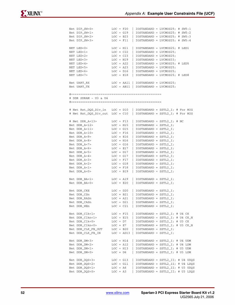
Net PUSH_BUTTON<0> LOC = N5 | IOSTANDARD = LVCMOS33; # SW3 - User PB1Net PUSH_BUTTON<1> LOC = K22 | IOSTANDARD = LVCMOS33; # SW2 - User PB2 Net DIP_SW<0> LOC = F20 | IOSTANDARD = LVCMOS25; # SW5:1Net DIP_SW<1> LOC = G19 | IOSTANDARD = LVCMOS25; # SW5:2Net DIP_SW<2> LOC = B23 | IOSTANDARD = LVCMOS25; # SW5:3Net DIP_SW<3> LOC = F11 | IOSTANDARD = LVCMOS25; # SW5:4

Spartan-3 PCI Express Starter Board Kit v1.2 www.xilinx.com 29UG2565 July 21, 2006
R
Chapter 6
LEDs
OverviewThe Spartan-3 PCI Express board has eight user LEDs that are located along the top of the board, just to the right of the push-button switches.
OperationFigure 6-1 shows the basic circuit diagram for the LEDs on the Spartan-3 PCI Express board. A high logic level on the FPGA pin will turn the corresponding LED ON and a low logic level with turn the LED OFF.
ConnectionsA UCF example of the LED signals is listed below.
NET LED<0> LOC = H11 | IOSTANDARD = LVCMOS25; # LED1NET LED<1> LOC = C22 | IOSTANDARD = LVCMOS25;NET LED<2> LOC = C23 | IOSTANDARD = LVCMOS25;NET LED<3> LOC = N19 | IOSTANDARD = LVCMOS33;NET LED<4> LOC = A22 | IOSTANDARD = LVCMOS25; # LED5NET LED<5> LOC = A23 | IOSTANDARD = LVCMOS25;NET LED<6> LOC = D16 | IOSTANDARD = LVCMOS25;NET LED<7> LOC = E18 | IOSTANDARD = LVCMOS25; # LED8
Figure 6-1: Basic Circuit LED Diagram
100LED
x
30 www.xilinx.com Spartan-3 PCI Express Starter Board Kit v1.2UG2565 July 21, 2006
Chapter 6: LEDsR

Spartan-3 PCI Express Starter Board Kit v1.2 www.xilinx.com 31UG2565 July 21, 2006
R
Chapter 7
VGA Display Port
OverviewThe Spartan-3 PCI Express board includes a video display port through an on-board Philips TDA8777 Triple DAC. Although the DAC is capable of 10-bit resolution, only 8-bits per color (RGB) are connected to the FPGA. A DB15 connector (P2) is provided for easy connection to standard monitors.
OperationFigure 7-1 shows a functional diagram of the Video Port implemented on the Spartan-3 PCI Express board.
The FPGA is responsible for driving the video DAC with 8-bits of red, green, and blue. It must also provide the timing and control signals to both the DAC and monitor itself. The provided 25.175 MHz clock oscillator enables 640 x 480 VGA resolution.
Two jumpers, JP8 and JP11, are also part of this circuit. JP8 enables and disables the 25.175 MHz oscillator. When JP8 is set to pins 1–2, the oscillator is disabled. When it is set to pins 2–3, it is enabled. Jumper JP11 controls the power mode of the Video DAC. JP11 is open for normal DAC operation and jumpered closed to place the video DAC in power- save mode.
Figure 7-1: Video Port Functional Diagram
TDA8777Video DAC
HSYNC
FPGA
RED[7:0]
BLANK
VSYNC
GREEN[7:0]
BLUE[7:0]
CSYNC
RED
GREEN
BLUE
13
14
1
2
3
P2
DB15
25.175MHz
U30

32 www.xilinx.com Spartan-3 PCI Express Starter Board Kit v1.2UG2565 July 21, 2006
Chapter 7: VGA Display PortR
ConnectionsA UCF example of the Video Port is shown below.
NET DAC_B<0> LOC = W15 | IOSTANDARD = LVCMOS25;NET DAC_B<1> LOC = AA13 | IOSTANDARD = LVCMOS25;NET DAC_B<2> LOC = Y11 | IOSTANDARD = LVCMOS25; NET DAC_B<3> LOC = AB9 | IOSTANDARD = LVCMOS25;NET DAC_B<4> LOC = AA9 | IOSTANDARD = LVCMOS25; NET DAC_B<5> LOC = Y9 | IOSTANDARD = LVCMOS25;NET DAC_B<6> LOC = Y8 | IOSTANDARD = LVCMOS25;NET DAC_B<7> LOC = AB7 | IOSTANDARD = LVCMOS25;NET DAC_G<0> LOC = AA17 | IOSTANDARD = LVCMOS25;NET DAC_G<1> LOC = AA16 | IOSTANDARD = LVCMOS25;NET DAC_G<2> LOC = AC16 | IOSTANDARD = LVCMOS25;NET DAC_G<3> LOC = AB16 | IOSTANDARD = LVCMOS25;NET DAC_G<4> LOC = AB15 | IOSTANDARD = LVCMOS25;NET DAC_G<5> LOC = AA15 | IOSTANDARD = LVCMOS25;NET DAC_G<6> LOC = Y16 | IOSTANDARD = LVCMOS25;NET DAC_G<7> LOC = W16 | IOSTANDARD = LVCMOS25;NET DAC_R<0> LOC = AC21 | IOSTANDARD = LVCMOS25;NET DAC_R<1> LOC = AB21 | IOSTANDARD = LVCMOS25;NET DAC_R<2> LOC = AA20 | IOSTANDARD = LVCMOS25;NET DAC_R<3> LOC = AB20 | IOSTANDARD = LVCMOS25;NET DAC_R<4> LOC = Y18 | IOSTANDARD = LVCMOS25;NET DAC_R<5> LOC = AA18 | IOSTANDARD = LVCMOS25;NET DAC_R<6> LOC = AB17 | IOSTANDARD = LVCMOS25;NET DAC_R<7> LOC = AC17 | IOSTANDARD = LVCMOS25;NET DAC_HSYNC LOC = AB6 | IOSTANDARD = LVCMOS25; NET DAC_VSYNC LOC = AA7 | IOSTANDARD = LVCMOS25; NET DAC_CSYNC LOC = AA6 | IOSTANDARD = LVCMOS25;NET DAC_BLANK LOC = AD4 | IOSTANDARD = LVCMOS25;NET VIDEO_CLK LOC = AF14 | IOSTANDARD = LVCMOS25;
Related ResourcesFor more information about the Philips TDA8777 Video DAC, visit www.semiconductors.philips.com.

Spartan-3 PCI Express Starter Board Kit v1.2 www.xilinx.com 33UG2565 July 21, 2006
R
Chapter 8
RS-232 PORT
OverviewThe Spartan-3 PCI Express board provides a DCE compatible RS-232 serial port for connection to most computer serial ports.
OperationFigure 8-1 shows the connection between the FPGA and the DB9 connector. The FPGA supplies serial output data using 2.5V LVCMOS levels to the TI device, which in turn converts the logic value to the appropriate RS-232 voltage level. Similarly, the TI device converts the RS-232 serial input data to 2.5V LVCMOS levels for the FPGA.
ConnectionsA UCF example of the RS-232 serial port signals is listed below.
Net UART_RX LOC = AA11 | IOSTANDARD = LVCMOS25;Net UART_TX LOC = AB11 | IOSTANDARD = LVCMOS25;
Figure 8-1: RS 232 Serial Port Diagram
P1
2
3
1
5
AB11
AB11
UART_TXLevel
ShifterUART_RX
FPGA

34 www.xilinx.com Spartan-3 PCI Express Starter Board Kit v1.2UG2565 July 21, 2006
Chapter 8: RS-232 PORTR

Spartan-3 PCI Express Starter Board Kit v1.2 www.xilinx.com 35UG2565 July 21, 2006
R
Chapter 9
DDR SDRAM
OverviewThe Spartan-3 PCI Express Starter Kit board includes two 512 Mb (32M x 16) Micron Technology DDR SDRAM (MT46V32M16). This provides a 32-bit data interface to the Spartan-3 FPGA. All DDR SDRAM interface pins connect to the FPGA I/O Banks 0 and 1—with the exception of the DDR clock feedback pin, which is in Bank 5. These three FPGA banks and the DDR SDRAM chips are powered by 2.5V, generated by a PTH03000W regulator from the 3.3V supply rail of the board. The 1.25V reference voltage, common to the FPGA and DDR SDRAM, is generated using TPS51100.
All DDR SDRAM interface signals are terminated. An SSTL_2, I/O standard is used. The system supply for signal termination resistors uses the TPS51100, which sets the termination voltage equal to VREF and tracks variations in the DC level of VREF.
The DDR feedback clock pin DDR_CLK_FB (output Pin B20) is fed back into FPGA pin AD13 in I/O Bank 5 to have best access to one of the FPGA Digital Clock Managers (DCMs). This path is required when using the MicroBlaze OPB DDR controller. The MicroBlaze OPB DDR SDRAM controller IP core documentation is also available from within the EDK 8.1i development software.
OperationThe 512Mb DDR SDRAM is a high-speed CMOS, dynamic random-access memory containing 536,870,912 bits. It is internally configured as a quad-bank DRAM.
The 512Mb DDR SDRAM uses a double-data-rate architecture to achieve high-speed operation. The double-data-rate architecture is essentially a 2n-prefetch architecture with an interface designed to transfer two data words per clock cycle at the I/O pins. A single read or write access for the 512Mb DDR SDRAM effectively consists of a single 2n-bit wide, one-clock-cycle data transfer at the internal DRAM core and two corresponding n-bit wide, one-half-clock-cycle data transfers at the I/O pins.
A bidirectional data strobe (DQS) is transmitted externally, along with data, for use in data capture at the receiver. DQS is a strobe transmitted by the DDR SDRAM during READs and by the memory controller during WRITEs. DQS is edge-aligned with data for READs and center-aligned with data for WRITEs. The x16 offering has two data strobes, one for the lower byte and one for the upper byte.
The 512Mb DDR SDRAM operates from a differential clock (CK and CK#); the crossing of CK going HIGH and CK# going LOW will be referred to as the positive edge of CK. Commands (address and control signals) are registered at every positive edge of CK. Input data is registered on both edges of DQS, and output data is referenced to both edges of DQS, as well as to both edges of CK.

36 www.xilinx.com Spartan-3 PCI Express Starter Board Kit v1.2UG2565 July 21, 2006
Chapter 9: DDR SDRAMR
Read and write accesses to the DDR SDRAM are burst oriented; accesses start at a selected location and continue for a programmed number of locations in a programmed sequence. Accesses begin with the registration of an ACTIVE command, which may then be followed by a READ or WRITE command. The address bits registered coincident with the ACTIVE command are used to select the bank and row to be accessed. The address bits registered coincident with the READ or WRITE command are used to select the bank and the starting column location for the burst access.
The DDR SDRAM provides for programmable READ or WRITE burst lengths of 2, 4, or 8 locations. An auto precharge function may be enabled to provide a self-timed row precharge that is initiated at the end of the burst access.
As with standard SDR SDRAMs, the pipelined, multibank architecture of DDR SDRAMs allows for concurrent operation, thereby providing high effective bandwidth by hiding row precharge and activation time.
An auto refresh mode is provided, along with a power-saving power-down mode. All inputs are compatible with the JEDEC Standard for SSTL_2. All full drive option outputs are SSTL_2, Class II compatible.
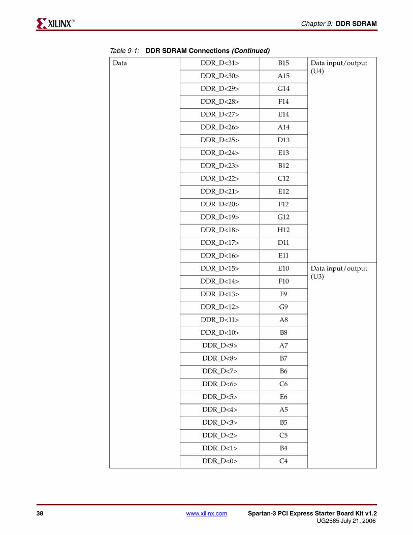
Table 9-1: DDR SDRAM Connections
CategoryDDR SDRAM Signal
NameFPGA Pin Number
Function
Address DDR_A<12> H15 Address Inputs
DDR_A<11> G15
DDR_A<10> F16
DDR_A<9> E16
DDR_A<8> H16
DDR_A<7> G16
DDR_A<6> E17
DDR_A<5> D17
DDR_A<4> G17
DDR_A<3> F17
DDR_A<2> G18
DDR_A<1> F18
DDR_A<0> B19
DDR_BA<1> A19 Bank address inputs
DDR_BA<0> E20

Spartan-3 PCI Express Starter Board Kit v1.2 www.xilinx.com 37UG2565 July 21, 2006
OperationR
Control DDR_CKE D20 Clock Enable
DDR_CSn B21 Chip select
DDR_RASn A21 Row address strobe
DDR_CASn D21 Column address strobe
DDR_WEn C21 Write enable
DDR_Clk<1> F15 Clock for upper 16-bits
DDR_Clkn<1> E15
DDR_Clk<0> D7 Clock for lower 16-bits
DDR_Clkn<0> E7
DDR_CLK_FB_OUT B20 Clock output feedback
DDR_CLK_FB_IN AD13 Clock input feedback
DDR_DM<3> H14 Data mask. Upper and lower data masks for each DDR chip
DDR_DM<2> A12
DDR_DM<1> H13
DDR_DM<0> D6
DDR_DQS<3> G13 Data strobe. Upper and lower data strobes for each DDR chip
DDR_DQS<2> G11
DDR_DQS<1> A6
DDR_DQS<0> A3
Table 9-1: DDR SDRAM Connections (Continued)
38 www.xilinx.com Spartan-3 PCI Express Starter Board Kit v1.2UG2565 July 21, 2006
Chapter 9: DDR SDRAMR
Data DDR_D<31> B15 Data input/output (U4)
DDR_D<30> A15
DDR_D<29> G14
DDR_D<28> F14
DDR_D<27> E14
DDR_D<26> A14
DDR_D<25> D13
DDR_D<24> E13
DDR_D<23> B12
DDR_D<22> C12
DDR_D<21> E12
DDR_D<20> F12
DDR_D<19> G12
DDR_D<18> H12
DDR_D<17> D11
DDR_D<16> E11
DDR_D<15> E10 Data input/output (U3)
DDR_D<14> F10
DDR_D<13> F9
DDR_D<12> G9
DDR_D<11> A8
DDR_D<10> B8
DDR_D<9> A7
DDR_D<8> B7
DDR_D<7> B6
DDR_D<6> C6
DDR_D<5> E6
DDR_D<4> A5
DDR_D<3> B5
DDR_D<2> C5
DDR_D<1> B4
DDR_D<0> C4
Table 9-1: DDR SDRAM Connections (Continued)

Spartan-3 PCI Express Starter Board Kit v1.2 www.xilinx.com 39UG2565 July 21, 2006
UCFR
UCF
AddressListed below are the UCF constraints for the DDR SDRAM address pins, including the I/O pin assignment and the I/O standard used.
Net DDR_A<12> LOC = H15 | IOSTANDARD = SSTL2_I; Net DDR_A<11> LOC = G15 | IOSTANDARD = SSTL2_I; Net DDR_A<10> LOC = F16 | IOSTANDARD = SSTL2_I; Net DDR_A<9> LOC = E16 | IOSTANDARD = SSTL2_I; Net DDR_A<8> LOC = H16 | IOSTANDARD = SSTL2_I; Net DDR_A<7> LOC = G16 | IOSTANDARD = SSTL2_I; Net DDR_A<6> LOC = E17 | IOSTANDARD = SSTL2_I; Net DDR_A<5> LOC = D17 | IOSTANDARD = SSTL2_I; Net DDR_A<4> LOC = G17 | IOSTANDARD = SSTL2_I; Net DDR_A<3> LOC = F17 | IOSTANDARD = SSTL2_I; Net DDR_A<2> LOC = G18 | IOSTANDARD = SSTL2_I; Net DDR_A<1> LOC = F18 | IOSTANDARD = SSTL2_I; Net DDR_A<0> LOC = B19 | IOSTANDARD = SSTL2_I; Net DDR_BA<1> LOC = A19 | IOSTANDARD = SSTL2_I; Net DDR_BA<0> LOC = E20 | IOSTANDARD = SSTL2_I;
ControlListed below are the UCF constraints for the DDR SDRAM control pins, including the I/O pin assignment and the I/O standard used.
Net DDR_CKE LOC = D20 | IOSTANDARD = SSTL2_I; Net DDR_CSn LOC = B21 | IOSTANDARD = SSTL2_I; Net DDR_RASn LOC = A21 | IOSTANDARD = SSTL2_I; Net DDR_CASn LOC = D21 | IOSTANDARD = SSTL2_I; Net DDR_WEn LOC = C21 | IOSTANDARD = SSTL2_I; Net DDR_Clk<1> LOC = F15 | IOSTANDARD = SSTL2_I; # U4 CK Net DDR_Clkn<1> LOC = E15 | IOSTANDARD = SSTL2_I; # U4 CK_N Net DDR_Clk<0> LOC = D7 | IOSTANDARD = SSTL2_I; # U3 CK Net DDR_Clkn<0> LOC = E7 | IOSTANDARD = SSTL2_I; # U3 CK_N Net DDR_CLK_FB_OUT LOC = B20 | IOSTANDARD = SSTL2_I; Net DDR_CLK_FB_IN LOC = AD13 | IOSTANDARD = SSTL2_I; Net DDR_DM<3> LOC = H14 | IOSTANDARD = SSTL2_I; # U4 UDM Net DDR_DM<2> LOC = A12 | IOSTANDARD = SSTL2_I; # U4 LDM Net DDR_DM<1> LOC = H13 | IOSTANDARD = SSTL2_I; # U3 UDM Net DDR_DM<0> LOC = D6 | IOSTANDARD = SSTL2_I; # U3 LDM Net DDR_DQS<3> LOC = G13 | IOSTANDARD = SSTL2_II; # U4 UDQS Net DDR_DQS<2> LOC = G11 | IOSTANDARD = SSTL2_II; # U4 LDQS Net DDR_DQS<1> LOC = A6 | IOSTANDARD = SSTL2_II; # U3 UDQS Net DDR_DQS<0> LOC = A3 | IOSTANDARD = SSTL2_II; # U3 LDQS
DataThis section provides the UCF constraints for the DDR SDRAM data pins, including the I/O pin assignment and the I/O standard used.

40 www.xilinx.com Spartan-3 PCI Express Starter Board Kit v1.2UG2565 July 21, 2006
Chapter 9: DDR SDRAMR
Net DDR_D<31> LOC = B15 | IOSTANDARD = SSTL2_II; # U4 DQ15 Net DDR_D<30> LOC = A15 | IOSTANDARD = SSTL2_II; Net DDR_D<29> LOC = G14 | IOSTANDARD = SSTL2_II; Net DDR_D<28> LOC = F14 | IOSTANDARD = SSTL2_II; Net DDR_D<27> LOC = E14 | IOSTANDARD = SSTL2_II; Net DDR_D<26> LOC = A14 | IOSTANDARD = SSTL2_II; Net DDR_D<25> LOC = D13 | IOSTANDARD = SSTL2_II; Net DDR_D<24> LOC = E13 | IOSTANDARD = SSTL2_II; Net DDR_D<23> LOC = B12 | IOSTANDARD = SSTL2_II; Net DDR_D<22> LOC = C12 | IOSTANDARD = SSTL2_II; Net DDR_D<21> LOC = E12 | IOSTANDARD = SSTL2_II; Net DDR_D<20> LOC = F12 | IOSTANDARD = SSTL2_II; Net DDR_D<19> LOC = G12 | IOSTANDARD = SSTL2_II; Net DDR_D<18> LOC = H12 | IOSTANDARD = SSTL2_II; Net DDR_D<17> LOC = D11 | IOSTANDARD = SSTL2_II; Net DDR_D<16> LOC = E11 | IOSTANDARD = SSTL2_II; # U4 DQ0 Net DDR_D<15> LOC = E10 | IOSTANDARD = SSTL2_II; # U3 DQ15 Net DDR_D<14> LOC = F10 | IOSTANDARD = SSTL2_II; Net DDR_D<13> LOC = F9 | IOSTANDARD = SSTL2_II; Net DDR_D<12> LOC = G9 | IOSTANDARD = SSTL2_II; Net DDR_D<11> LOC = A8 | IOSTANDARD = SSTL2_II; Net DDR_D<10> LOC = B8 | IOSTANDARD = SSTL2_II; Net DDR_D<9> LOC = A7 | IOSTANDARD = SSTL2_II; Net DDR_D<8> LOC = B7 | IOSTANDARD = SSTL2_II; Net DDR_D<7> LOC = B6 | IOSTANDARD = SSTL2_II; Net DDR_D<6> LOC = C6 | IOSTANDARD = SSTL2_II; Net DDR_D<5> LOC = E6 | IOSTANDARD = SSTL2_II; Net DDR_D<4> LOC = A5 | IOSTANDARD = SSTL2_II; Net DDR_D<3> LOC = B5 | IOSTANDARD = SSTL2_II; Net DDR_D<2> LOC = C5 | IOSTANDARD = SSTL2_II; Net DDR_D<1> LOC = B4 | IOSTANDARD = SSTL2_II; Net DDR_D<0> LOC = C4 | IOSTANDARD = SSTL2_II; # U3 DQ0
Related ResourcesBelow listed are related resources. Click any of the following links to download the desired documention.
Xilinx Embedded Design Kit (EDK)
MT46V32M16 (32M x 16) DDR SDRAM Data Sheet
MicroBlaze OPB Double Data Rate (DDR) SDRAM Controller (v2.00b)

Spartan-3 PCI Express Starter Board Kit v1.2 www.xilinx.com 41UG2565 July 21, 2006
R
Chapter 10
SPI Serial Flash
OverviewThe Spartan-3 PCI Express board includes a STMicroelectronics M25P40 4 Mb SPI serial Flash, useful in a variety of applications, such as:
• Simple non-volatile data storage
• Storage for identifier codes, serial numbers, IP addresses, etc.
• Storage of MicroBlaze processor code that can be shadowed into DDR SDRAM.
OperationThe M25P40 is a 4 Mb (512K x 8) Serial Flash Memory, with advanced write protection mechanisms, accessed by a high speed SPI-compatible bus.
The memory can be programmed 1 to 256 bytes at a time, using the Page Program instruction. The memory is organized as 8 sectors, each containing 256 pages. Each page is 256 bytes wide. Thus, the whole memory can be viewed as consisting of 2048 pages, or 524,288 bytes. The whole memory can be erased using the Bulk Erase instruction, or a sector at a time, using the Sector Erase instruction.
On the Spartan-3 PCI Express board, the SPI Serial Flash signals are placed in Banks 2 and 3. These banks have an adjustable I/O voltage to add flexibility to the EXP connector. Therefore, the FPGA I/O voltage could be either 2.5V or 3.3V, depending on the setting of JP5. Voltage translator buffers are used to enable the 3.3V serial flash to connect to the FPGA. The SPROM_EN signal turns on these translator buffers. If the design uses the serial flash, this signal must be asserted.
The SPI Serial Flash can be programmed directly by the FPGA using MicroBlazeTM or PicoBlazeTM. The serial flash pins can also be accessed through connector J6. This is compatible with the Xilinx XSPI programming utility (see XAPP445) and iMPACT 8.2i. To enable serial flash programming via the J6 JTAG connector, the FPGA must drive the SPROM_ENABLE pin (K6) from the FPGA to a logic level low. When SPROM_ENABLE is

42 www.xilinx.com Spartan-3 PCI Express Starter Board Kit v1.2UG2565 July 21, 2006
Chapter 10: SPI Serial FlashR
driven high, the FPGA has access to the Serial Flash interface. Figure 10-1 shows the Serial Flash connection options.
ConnectionsA UCF example of the SPI Serial Flash is shown below.
#================================================= # SPI PROM - U33 #================================================= # IOSTANDARD depends on JP5 jumper selection except "SPROM_EN" Net SPROM_DIN LOC = P19 | IOSTANDARD = LVCMOS25/33; Net SPROM_DOUT LOC = M22 | IOSTANDARD = LVCMOS25/33; Net SPROM_EN LOC = K6 | IOSTANDARD = LVCMOS33; Net SPROM_CSn LOC = P23 | IOSTANDARD = LVCMOS25/33; Net SPROM_CLK LOC = M21 | IOSTANDARD = LVCMOS25/33;
Related ResourcesClick on the following links to download the desired supporting documentation.
STMicro M25P40 Data Sheet
Xilinx Application Note XAPP445
Figure 10-1: Serial Flash Interfaces
SPROM_DIN
FPGASPROM_DOUTSPROM_CLKSPROM_CS#
TDI
JTAGConnector
TDOTCLKTMS
SerialFlash
Memory
SerialFlash
Memory
J6
SPROM_ENABLE_1
SPROM_ENABLE_0

Spartan-3 PCI Express Starter Board Kit v1.2 www.xilinx.com 43UG2565 July 21, 2006
R
Chapter 11
FPGA Configuration
OverviewThe Spartan-3 PCI Express Starter Kit board supports two FPGA configuration options:
• Download FPGA designs directly to the Spartan-3 FPGA via JTAG, using the download cable interface.
• Program the on-board 8 Mb Xilinx XCF08P parallel Platform Flash PROM, then configure the FPGA from the image stored in the Platform Flash PROM using either Master Serial or Master SelectMAP (Parallel) modes.
The configuration mode jumpers determine which configuration mode the FPGA uses when power is first applied, or whenever the PROG button is pressed. The DONE pin LED lights when the FPGA successfully finishes configuration. Pressing the PROG button forces the FPGA to restart its configuration process.
The JTAG download cable interface supports the Xilinx USB-JTAG and the Parallel Cable IV. Xilinx Parallel Cable III or Memec IJC-x cables are not supported. This interface also provides in-system programming for the on-board Platform Flash PROM. This interface is accessed through connector socket J2.
Note: Do not confuse the J2 socket with the Serial Flash programming socket (J6), which is identical.
The 8 Mb Xilinx Platform Flash PROM provides easy, JTAG-programmable configuration storage for the FPGA. The FPGA configures from the Platform Flash using either Master Serial or Master SelectMAP modes.

44 www.xilinx.com Spartan-3 PCI Express Starter Board Kit v1.2UG2565 July 21, 2006
Chapter 11: FPGA ConfigurationR
Operation
Configuration Mode jumpersAs shown in Table 11-1, the JP3 jumper block settings control the FPGA configuration mode. Inserting a jumper grounds the associated mode pin. Insert or remove individual jumpers to select the FPGA configuration mode and associated configuration source.
PROG SwitchSW1 causes a toggling of the PROG signal on the FPGA, which forces a reconfiguraton based on the current setting of the Mode jumpers.
DONE LEDD14 is the DONE LED. If the FPGA successfully configures, then DONE is asserted, which causes D14 to be lit. This is the only blue colored LED on the board.
Using the Platform Flash for User StorageThe Spartan-3 PCI Express board provides the necessary connections to allow you to use the Platform Flash for user storage (as discussed in XAPP694).
Jumper J4 makes the connection between PROM_CE# and FPGA_DONE. Under typical PROM operation, this jumper should be installed. However, to exercise the technique discussed in XAPP694, this jumper is removed.
This board also provides signals FPGA_PROM_READ, FPGA_to_PROM_CCLK, and FPGA_to_PROM_CE#, also used when implemented as described in XAPP694.
Reprogramming Platform Flash from the FPGAThe Spartan-3 PCI Express board provides connections between FPGA I/Os and the JTAG chain. This makes possible the creation of a design (like MicroBlaze) to reprogram the Platform Flash PROM from the FPGA (see XAPP058). These signals include FPGA_to_PROM, FPGA_TDI_to_PROM, FPGA_TCK_to_PROM, FPGA_TMS_to_PROM, and PROM_TDO_to_FPGA.
Table 11-1: Configuration Mode Jumper Settings
Configuration ModeMode PinsM2:M1:M0
FPGA Configuration Image Source
Jumper Settings
JTAG 1:1:1 J6 programming socket
M1 installed
Master Serial 0:0:0 Platform flash in serial mode (DO only)
M0, M1, M2 installed
Master SelectMAP 0:1:1 Platform flash in parallel mode (D[07]used)
M2 installed

Spartan-3 PCI Express Starter Board Kit v1.2 www.xilinx.com 45UG2565 July 21, 2006
ConnectionsR
ConnectionsA UCF example listed below.
#=================================================# Platform Flash PROM Config (JTAG) - U24#=================================================
Net FPGA_to_PROM LOC = AA10 | IOSTANDARD = LVCMOS25;Net FPGA_TDI_to_PROM LOC = W12 | IOSTANDARD = LVCMOS25;Net FPGA_TCK_to_PROM LOC = Y13 | IOSTANDARD = LVCMOS25;Net FPGA_TMS_to_PROM LOC = W13 | IOSTANDARD = LVCMOS25;Net PROM_TDO_to_FPGA LOC = AB10 | IOSTANDARD = LVCMOS25;
# IOSTANDARD depends on JP5 jumper selectionNet FPGA_PROM_READ LOC = R20 | IOSTANDARD = LVCMOS25/33;Net FPGA_to_PROM_CCLK LOC = AB10 | IOSTANDARD = LVCMOS25/33;Net FPGA_to_PROM_CE LOC = AC25 | IOSTANDARD = LVCMOS25/33;
Related ResourcesClick the links below to download related documentation.
Xilinx Platform Flash Data Sheet
Xilinx Application Note XAPP694
Xilinx Application Note XAPP058

46 www.xilinx.com Spartan-3 PCI Express Starter Board Kit v1.2UG2565 July 21, 2006
Chapter 11: FPGA ConfigurationR

Spartan-3 PCI Express Starter Board Kit v1.2 www.xilinx.com 47UG2565 July 21, 2006
R
Chapter 12
Power Supplies
OverviewThe Spartan-3 PCI Express board provides complete and stable power for all components on the board as well as the EXP expansion connectors. The board can be powered from multiple sources, such as:
• 3.3V PCI Express edge connector
• 5V ATX power supply disk drive socket (supply not provided in the Starter Kit)
• 5V barrel jack (supply not provided in the Starter Kit)
The input source is selected by the position of a fuse on the board.
Input Power RegulationsSeveral power rails are regulated based on the input power.
5V to 3.3V Regulation
A PTH050101W DC/DC switching module provides 5V to 3.3V conversion when either the disk drive or barrel jack is used to provide 5V input power. The PTH050101W is capable of producing 15A of output voltage. A TPS3828 provides input voltage tracking.
If a barrel jack is used, then SW6 allows the user to switch power on and off without unplugging the supply.
3.3V is used for the I/O voltage on the FPGA, source voltage for EXP, the Video DAC, the SPI Serial Flash, the clocks oscillators, RS-232, LEDs, switches, and PX1011A PHY VDD1.
3.3V to 2.5V Regulation
A PTH03000W DC/DC switching module provides 3.3V to 2.5V conversion with a maximum output of 6A.
2.5V is used for the I/O voltage on the FPGA, source voltage for EXP, the DDR, Platform Flash I/O, the JTAG chain, and PX1011A PHY VDD2.
3.3V to 1.2V Regulation
A PTH03000W DC/DC switching module provides 3.3V to 1.2V conversion with a maximum output of 6A.
1.2V is used for the FPGA internal voltage and the PX1011A PHY VDD4.

48 www.xilinx.com Spartan-3 PCI Express Starter Board Kit v1.2UG2565 July 21, 2006
Chapter 12: Power SuppliesR
2.5V to 1.8V Regulation
A TPS72501 DC/DC linear regulator provides 2.5V to 1.8V conversion with a maximum output of 1A.
1.8V is used for the Platform Flash internal voltage.
1.25V Regulation
1.25V is needed for the PX1011A PHY reference voltage, the DDR reference voltage, and the PHY and DDR termination tracking voltage.
The TPS736125 linear regulator produces the 1.25V PHY reference voltage from 2.5V.
The TPS51100 produces both the 1.25V reference for the DDR as well as the 1.25V termination tracking voltage for both the PHY and the DDR. The TPS51100 has a 2.5V source input and a 5V reference input. Figure 12-1 is a diagram of the SSTL2 termination.
5V to 3.3V Regulation
A TPS60131 boost regulator provides 5V from 3.3V. This is necessary in the scenario that the PCI Express edge connector is the source voltage.
This 5V is used as a reference to the termination tracking voltage regulator. It is also used as a source voltage for the POWER GOOD LEDs.
Voltage SupervisionThe TPS3126 and TPS3307 devices provide voltage supervision for the board. 1.2V, 1.8V, 2.5V, and 3.3V are monitored. When all of these supplies have regulated properly, the PROG signal to the FPGA is released such that configuration can begin. Pressing SW1 causes a reset on the TPS3126 supervisor, which in turn causes PROG to be toggled causing a reconfiguration.
Figure 12-1: SSTL2 Termination Diagram
25 ohm
Spartan-3/Spartan-3EFPGA
PX1011APHY
Rx
Tx
Tx
Rx
25_ohm
50 ohm 50 ohm
SSTL2_11
+1.25V_TT
TPS51100TerminationRegulator

Spartan-3 PCI Express Starter Board Kit v1.2 www.xilinx.com 49UG2565 July 21, 2006
OperationR
OperationWhen power is properly applied to the board, the following POWER GOOD LEDs are lit:
• D12 for 1.2V
• D15 for 1.25V Termination Voltage
• D11 for 2.5V
• D13 for 3.3V
PCI Express Edge Connector as Source1. Place the fuse in socket F2. Do NOT place a separate fuse in F1 or damage may occur
to the board.
2. Plug the board into the PC.
3. When power is applied to the PC, power will immediately be distributed to the board.
Disk Drive Connector as Source1. Place the fuse in socket F1. Do NOT place a separate fuse in F2 or damage may occur
to the board.
2. Plug the board into the PC.
3. Plug in a spare disk drive connector to socket J1 on the board.
4. When power is applied to the PC, power will immediately be distributed to the board.
Barrel Jack as SourceThis mode is intended for benchtop operation only. This is useful for programming the PROM or working on a non-PCI Express design.
1. Place the fuse in socket F1. Do NOT place a separate fuse in F2 or damage may occur to the board.
2. Insert a 5V source into the barrel jack.
3. Move the power switch to the ON position.
Related ResourcesClick the link below to download related documentation.
TI Power References

50 www.xilinx.com Spartan-3 PCI Express Starter Board Kit v1.2UG2565 July 21, 2006
Chapter 12: Power SuppliesR

Spartan-3 PCI Express Starter Board Kit v1.2 www.xilinx.com 51UG2565 July 21, 2006
Appendix A
Example User Constraints File (UCF)
#---------------------------------------------------------------------# MASTER Constraints File for the Xilinx Spartan-3 PCIe Starter Board:##---------------------------------------------------------------------
#---------------------------------------------------------------------# Xilinx Technology : Spartan-3# Part : XC3S1000# Package : FG676# Speed Grade : -4#---------------------------------------------------------------------# Revision : 1.0 <Original Release># Date : 3/01/2006# Project : #=====================================================================
#*********************************************************************# *# DISCLAIMER: *# Avnet, Inc. makes no warranty for the use of this code*# or design. This code is provided "As Is". Avnet,Inc *# assumes no responsibility for any errors, which may * # appear in this code, nor does it make a commitment *# to update the information contained herein. *# Avnet, Inc specifically disclaims any implied *# warranties of fitness for a particular purpose. *# *#*********************************************************************
###################################################################### # User Constraints (Pinout, Placement, Etc.)######################################################################
#=================================================# CLOCKS, SWITCHES, LEDS, RS323(UART)#=================================================
Net CLK_50MHZ LOC = A13 | IOSTANDARD = LVCMOS25; # U20 - 50MHz OSCNet CLK_SOCKET LOC = B14 | IOSTANDARD = LVCMOS25; # U10 - 3.3V OSC SocketNet CLK_SMT LOC = C14 | IOSTANDARD = LVCMOS25; # U26 - 3.3V OSC SMT Net FPGA_RESETn LOC = F21 | IOSTANDARD = LVCMOS25; # Push button SW4 Net PUSH_BUTTON<0> LOC = N5 | IOSTANDARD = LVCMOS33; # SW3 - User PB1Net PUSH_BUTTON<1> LOC = K22 | IOSTANDARD = LVCMOS33; # SW2 - User PB2
52 www.xilinx.com Spartan-3 PCI Express Starter Board Kit v1.2UG2565 July 21, 2006
Appendix A: Example User Constraints File (UCF)R
Net DIP_SW<0> LOC = F20 | IOSTANDARD = LVCMOS25; # SW5:1Net DIP_SW<1> LOC = G19 | IOSTANDARD = LVCMOS25; # SW5:2Net DIP_SW<2> LOC = B23 | IOSTANDARD = LVCMOS25; # SW5:3Net DIP_SW<3> LOC = F11 | IOSTANDARD = LVCMOS25; # SW5:4 NET LED<0> LOC = H11 | IOSTANDARD = LVCMOS25; # LED1NET LED<1> LOC = C22 | IOSTANDARD = LVCMOS25;NET LED<2> LOC = C23 | IOSTANDARD = LVCMOS25;NET LED<3> LOC = N19 | IOSTANDARD = LVCMOS33;NET LED<4> LOC = A22 | IOSTANDARD = LVCMOS25; # LED5NET LED<5> LOC = A23 | IOSTANDARD = LVCMOS25;NET LED<6> LOC = D16 | IOSTANDARD = LVCMOS25;NET LED<7> LOC = E18 | IOSTANDARD = LVCMOS25; # LED8 Net UART_RX LOC = AA11 | IOSTANDARD = LVCMOS25;Net UART_TX LOC = AB11 | IOSTANDARD = LVCMOS25;
#=================================================# DDR SDRAM - U3 & U4#=================================================
# Net Rst_DQS_Div_in LOC = D10 | IOSTANDARD = SSTL2_I; # For MIG# Net Rst_DQS_Div_out LOC = C10 | IOSTANDARD = SSTL2_I; # For MIG
# Net DDR_A<13> LOC = F13 | IOSTANDARD = SSTL2_I; # NC Net DDR_A<12> LOC = H15 | IOSTANDARD = SSTL2_I; Net DDR_A<11> LOC = G15 | IOSTANDARD = SSTL2_I; Net DDR_A<10> LOC = F16 | IOSTANDARD = SSTL2_I; Net DDR_A<9> LOC = E16 | IOSTANDARD = SSTL2_I;Net DDR_A<8> LOC = H16 | IOSTANDARD = SSTL2_I;Net DDR_A<7> LOC = G16 | IOSTANDARD = SSTL2_I;Net DDR_A<6> LOC = E17 | IOSTANDARD = SSTL2_I;Net DDR_A<5> LOC = D17 | IOSTANDARD = SSTL2_I;Net DDR_A<4> LOC = G17 | IOSTANDARD = SSTL2_I;Net DDR_A<3> LOC = F17 | IOSTANDARD = SSTL2_I;Net DDR_A<2> LOC = G18 | IOSTANDARD = SSTL2_I;Net DDR_A<1> LOC = F18 | IOSTANDARD = SSTL2_I; Net DDR_A<0> LOC = B19 | IOSTANDARD = SSTL2_I;
Net DDR_BA<1> LOC = A19 | IOSTANDARD = SSTL2_I; Net DDR_BA<0> LOC = E20 | IOSTANDARD = SSTL2_I;
Net DDR_CKE LOC = D20 | IOSTANDARD = SSTL2_I;Net DDR_CSn LOC = B21 | IOSTANDARD = SSTL2_I;Net DDR_RASn LOC = A21 | IOSTANDARD = SSTL2_I;Net DDR_CASn LOC = D21 | IOSTANDARD = SSTL2_I;Net DDR_WEn LOC = C21 | IOSTANDARD = SSTL2_I;
Net DDR_Clk<1> LOC = F15 | IOSTANDARD = SSTL2_I; # U4 CKNet DDR_Clkn<1> LOC = E15 | IOSTANDARD = SSTL2_I; # U4 CK_NNet DDR_Clk<0> LOC = D7 | IOSTANDARD = SSTL2_I; # U3 CKNet DDR_Clkn<0> LOC = E7 | IOSTANDARD = SSTL2_I; # U3 CK_NNet DDR_CLK_FB_OUT LOC = B20 | IOSTANDARD = SSTL2_I;Net DDR_CLK_FB_IN LOC = AD13 | IOSTANDARD = SSTL2_I;
Net DDR_DM<3> LOC = H14 | IOSTANDARD = SSTL2_I; # U4 UDMNet DDR_DM<2> LOC = A12 | IOSTANDARD = SSTL2_I; # U4 LDMNet DDR_DM<1> LOC = H13 | IOSTANDARD = SSTL2_I; # U3 UDMNet DDR_DM<0> LOC = D6 | IOSTANDARD = SSTL2_I; # U3 LDM
Net DDR_DQS<3> LOC = G13 | IOSTANDARD = SSTL2_II; # U4 UDQSNet DDR_DQS<2> LOC = G11 | IOSTANDARD = SSTL2_II; # U4 LDQSNet DDR_DQS<1> LOC = A6 | IOSTANDARD = SSTL2_II; # U3 UDQSNet DDR_DQS<0> LOC = A3 | IOSTANDARD = SSTL2_II; # U3 LDQS

Spartan-3 PCI Express Starter Kit User Guide www.xilinx.com 53UG2565 July 21, 2006
R
Net DDR_D<31> LOC = B15 | IOSTANDARD = SSTL2_II; # U4 DQ15Net DDR_D<30> LOC = A15 | IOSTANDARD = SSTL2_II;Net DDR_D<29> LOC = G14 | IOSTANDARD = SSTL2_II;Net DDR_D<28> LOC = F14 | IOSTANDARD = SSTL2_II;Net DDR_D<27> LOC = E14 | IOSTANDARD = SSTL2_II;Net DDR_D<26> LOC = A14 | IOSTANDARD = SSTL2_II;Net DDR_D<25> LOC = D13 | IOSTANDARD = SSTL2_II;Net DDR_D<24> LOC = E13 | IOSTANDARD = SSTL2_II;Net DDR_D<23> LOC = B12 | IOSTANDARD = SSTL2_II;Net DDR_D<22> LOC = C12 | IOSTANDARD = SSTL2_II;Net DDR_D<21> LOC = E12 | IOSTANDARD = SSTL2_II;Net DDR_D<20> LOC = F12 | IOSTANDARD = SSTL2_II;Net DDR_D<19> LOC = G12 | IOSTANDARD = SSTL2_II;Net DDR_D<18> LOC = H12 | IOSTANDARD = SSTL2_II;Net DDR_D<17> LOC = D11 | IOSTANDARD = SSTL2_II;Net DDR_D<16> LOC = E11 | IOSTANDARD = SSTL2_II; # U4 DQ0 Net DDR_D<15> LOC = E10 | IOSTANDARD = SSTL2_II; # U3 DQ15Net DDR_D<14> LOC = F10 | IOSTANDARD = SSTL2_II;Net DDR_D<13> LOC = F9 | IOSTANDARD = SSTL2_II;Net DDR_D<12> LOC = G9 | IOSTANDARD = SSTL2_II;Net DDR_D<11> LOC = A8 | IOSTANDARD = SSTL2_II;Net DDR_D<10> LOC = B8 | IOSTANDARD = SSTL2_II;Net DDR_D<9> LOC = A7 | IOSTANDARD = SSTL2_II;Net DDR_D<8> LOC = B7 | IOSTANDARD = SSTL2_II;Net DDR_D<7> LOC = B6 | IOSTANDARD = SSTL2_II;Net DDR_D<6> LOC = C6 | IOSTANDARD = SSTL2_II;Net DDR_D<5> LOC = E6 | IOSTANDARD = SSTL2_II;Net DDR_D<4> LOC = A5 | IOSTANDARD = SSTL2_II;Net DDR_D<3> LOC = B5 | IOSTANDARD = SSTL2_II;Net DDR_D<2> LOC = C5 | IOSTANDARD = SSTL2_II;Net DDR_D<1> LOC = B4 | IOSTANDARD = SSTL2_II;Net DDR_D<0> LOC = C4 | IOSTANDARD = SSTL2_II; # U3 DQ0
#=================================================# Video DAC - U30#=================================================
NET DAC_B<0> LOC = W15 | IOSTANDARD = LVCMOS25;NET DAC_B<1> LOC = AA13 | IOSTANDARD = LVCMOS25;NET DAC_B<2> LOC = Y11 | IOSTANDARD = LVCMOS25; NET DAC_B<3> LOC = AB9 | IOSTANDARD = LVCMOS25;NET DAC_B<4> LOC = AA9 | IOSTANDARD = LVCMOS25; NET DAC_B<5> LOC = Y9 | IOSTANDARD = LVCMOS25;NET DAC_B<6> LOC = Y8 | IOSTANDARD = LVCMOS25;NET DAC_B<7> LOC = AB7 | IOSTANDARD = LVCMOS25;NET DAC_G<0> LOC = AA17 | IOSTANDARD = LVCMOS25;NET DAC_G<1> LOC = AA16 | IOSTANDARD = LVCMOS25;NET DAC_G<2> LOC = AC16 | IOSTANDARD = LVCMOS25;NET DAC_G<3> LOC = AB16 | IOSTANDARD = LVCMOS25;NET DAC_G<4> LOC = AB15 | IOSTANDARD = LVCMOS25;NET DAC_G<5> LOC = AA15 | IOSTANDARD = LVCMOS25;NET DAC_G<6> LOC = Y16 | IOSTANDARD = LVCMOS25;NET DAC_G<7> LOC = W16 | IOSTANDARD = LVCMOS25;NET DAC_R<0> LOC = AC21 | IOSTANDARD = LVCMOS25;NET DAC_R<1> LOC = AB21 | IOSTANDARD = LVCMOS25;NET DAC_R<2> LOC = AA20 | IOSTANDARD = LVCMOS25;NET DAC_R<3> LOC = AB20 | IOSTANDARD = LVCMOS25;NET DAC_R<4> LOC = Y18 | IOSTANDARD = LVCMOS25;NET DAC_R<5> LOC = AA18 | IOSTANDARD = LVCMOS25;NET DAC_R<6> LOC = AB17 | IOSTANDARD = LVCMOS25;NET DAC_R<7> LOC = AC17 | IOSTANDARD = LVCMOS25;NET DAC_HSYNC LOC = AB6 | IOSTANDARD = LVCMOS25; NET DAC_VSYNC LOC = AA7 | IOSTANDARD = LVCMOS25;

54 www.xilinx.com Spartan-3 PCI Express Starter Board Kit v1.2UG2565 July 21, 2006
Appendix A: Example User Constraints File (UCF)R
NET DAC_CSYNC LOC = AA6 | IOSTANDARD = LVCMOS25;NET DAC_BLANK LOC = AD4 | IOSTANDARD = LVCMOS25;NET VIDEO_CLK LOC = AF14 | IOSTANDARD = LVCMOS25;
#=================================================# SPI PROM - U33#=================================================
# IOSTANDARD depends on JP5 jumper selection except "SPROM_EN"
Net SPROM_DIN LOC = P19 ;Net SPROM_DOUT LOC = M22 ;Net SPROM_EN LOC = K6 | IOSTANDARD = LVCMOS33;Net SPROM_CSn LOC = P23 ;Net SPROM_CLK LOC = M21 ;
#=================================================# Platform Flash PROM Config (JTAG) - U24#=================================================
Net FPGA_to_PROM LOC = AA10 | IOSTANDARD = LVCMOS25;Net FPGA_TDI_to_PROM LOC = W12 | IOSTANDARD = LVCMOS25;Net FPGA_TCK_to_PROM LOC = Y13 | IOSTANDARD = LVCMOS25;Net FPGA_TMS_to_PROM LOC = W13 | IOSTANDARD = LVCMOS25;Net PROM_TDO_to_FPGA LOC = AB10 | IOSTANDARD = LVCMOS25;
#=================================================# SPI PROM - U5#=================================================
# IOSTANDARD depends on JP5 jumper selection
Net ID_DATA LOC = T5;
#=================================================# 8-bit AVR Microcontroller - U8#=================================================
# IOSTANDARD depends on JP5 jumper selection
Net ATTINY_TX LOC = V2;Net ATTINY_RX LOC = U6;Net ATTINY_RSTn LOC = U5;Net ATTINY_CLK LOC = V3;
#=================================================# EXP I/O - Connector JX1#=================================================
# IOSTANDARD depends on JP5 jumper selection
Net JX1_SE_IO_0 LOC = M3 ; # B6GIO_0Net JX1_SE_IO_1 LOC = J7 ; # B7GIO_0Net JX1_SE_IO_2 LOC = M7 ; # B6GIO_1Net JX1_SE_IO_3 LOC = J6 ; # B7GIO_1Net JX1_SE_IO_4 LOC = N7 ; # B6GIO_2Net JX1_SE_IO_5 LOC = H5 ; # B7GIO_2Net JX1_SE_IO_6 LOC = M8 ; # B6GIO_3Net JX1_SE_IO_7 LOC = H2 ; # B7GIO_3Net JX1_SE_IO_8 LOC = N8 ; # B6GIO_4Net JX1_SE_IO_9 LOC = J5 ; # B7GIO_4Net JX1_SE_IO_10 LOC = P8 ; # B6GIO_5Net JX1_SE_IO_11 LOC = J4 ; # B7GIO_5Net JX1_SE_IO_12 LOC = P2 ; # B6GIO_6Net JX1_SE_IO_13 LOC = K7 ; # B7GIO_6

Spartan-3 PCI Express Starter Kit User Guide www.xilinx.com 55UG2565 July 21, 2006
R
Net JX1_SE_IO_14 LOC = P7 ; # B6GIO_7Net JX1_SE_IO_15 LOC = K5 ; # B7GIO_7Net JX1_SE_IO_16 LOC = R1 ; # B6GIO_8Net JX1_SE_IO_17 LOC = L8 ; # B7GIO_8Net JX1_SE_IO_18 LOC = P1 ; # B6GIO_9Net JX1_SE_IO_19 LOC = L7 ; # B7GIO_9Net JX1_SE_IO_20 LOC = R2 ; # B6GIO_10Net JX1_SE_IO_21 LOC = H1 ; # B7GIO_10Net JX1_SE_IO_22 LOC = R3 ; # B6GIO_11Net JX1_SE_IO_23 LOC = L1 ; # B7GIO_11Net JX1_SE_IO_24 LOC = T1 ; # B6GIO_12Net JX1_SE_IO_25 LOC = L2 ; # B7GIO_12Net JX1_SE_IO_26 LOC = T2 ; # B6GIO_13Net JX1_SE_IO_27 LOC = L4 ; # B7GIO_13Net JX1_SE_IO_28 LOC = V6 ; # B7GIO_14Net JX1_SE_IO_29 LOC = U7 ; # B7GIO_15Net JX1_SE_IO_30 LOC = W5 ; # B6GIO_14Net JX1_SE_IO_31 LOC = V7 ; # B6GIO_15Net JX1_SE_IO_32 LOC = R8 ; # B7GIO_17Net JX1_SE_IO_33 LOC = R7 ; # B7GIO_18
Net JX1_SE_CLK_IN LOC = B13 ; # B0_GCLK7Net JX1_SE_CLK_OUT LOC = T4 ; # B7GIO_16
Net JX1_DIFF_N_0 LOC = AB4 ; # B6GPIOn_0Net JX1_DIFF_N_1 LOC = W7 ; # B7GPIOn_0Net JX1_DIFF_N_2 LOC = AC2 ; # B6GPIOn_1Net JX1_DIFF_N_3 LOC = V5 ; # B7GPIOn_1Net JX1_DIFF_N_4 LOC = W4 ; # B6GPIOn_2Net JX1_DIFF_N_5 LOC = T8 ; # B7GPIOn_2Net JX1_DIFF_N_6 LOC = W2 ; # B6GPIOn_3Net JX1_DIFF_N_7 LOC = R6 ; # B7GPIOn_3Net JX1_DIFF_N_8 LOC = U4 ; # B6GPIOn_4Net JX1_DIFF_N_9 LOC = P6 ; # B7GPIOn_4Net JX1_DIFF_N_10 LOC = U2 ; # B6GPIOn_5Net JX1_DIFF_N_11 LOC = M6 ; # B7GPIOn_5Net JX1_DIFF_N_12 LOC = P4 ; # B6GPIOn_6Net JX1_DIFF_N_13 LOC = N3 ; # B7GPIOn_6Net JX1_DIFF_N_14 LOC = N1 ; # B6GPIOn_7Net JX1_DIFF_N_15 LOC = L5 ; # B7GPIOn_7Net JX1_DIFF_N_16 LOC = K1 ; # B6GPIOn_9Net JX1_DIFF_N_17 LOC = J2 ; # B7GPIOn_8Net JX1_DIFF_N_18 LOC = K3 ; # B6GPIOn_10Net JX1_DIFF_N_19 LOC = H3 ; # B7GPIOn_9Net JX1_DIFF_N_20 LOC = G1 ; # B6GPIOn_11Net JX1_DIFF_N_21 LOC = E3 ; # B7GPIOn_10
Net JX1_DIFF_P_0 LOC = AB3 ; # B6GPIOp_0Net JX1_DIFF_P_1 LOC = W6 ; # B7GPIOp_0Net JX1_DIFF_P_2 LOC = AC1 ; # B6GPIOp_1Net JX1_DIFF_P_3 LOC = V4 ; # B7GPIOp_1Net JX1_DIFF_P_4 LOC = W3 ; # B6GPIOp_2Net JX1_DIFF_P_5 LOC = T7 ; # B7GPIOp_2Net JX1_DIFF_P_6 LOC = W1 ; # B6GPIOp_3Net JX1_DIFF_P_7 LOC = R5 ; # B7GPIOp_3Net JX1_DIFF_P_8 LOC = U3 ; # B6GPIOp_4Net JX1_DIFF_P_9 LOC = P5 ; # B7GPIOp_4Net JX1_DIFF_P_10 LOC = U1 ; # B6GPIOp_5Net JX1_DIFF_P_11 LOC = M5 ; # B7GPIOp_5Net JX1_DIFF_P_12 LOC = P3 ; # B6GPIOp_6Net JX1_DIFF_P_13 LOC = N4 ; # B7GPIOp_6Net JX1_DIFF_P_14 LOC = N2 ; # B6GPIOp_7Net JX1_DIFF_P_15 LOC = L6 ; # B7GPIOp_7Net JX1_DIFF_P_16 LOC = K2 ; # B6GPIOp_9Net JX1_DIFF_P_17 LOC = J3 ; # B7GPIOp_8

56 www.xilinx.com Spartan-3 PCI Express Starter Board Kit v1.2UG2565 July 21, 2006
Appendix A: Example User Constraints File (UCF)R
Net JX1_DIFF_P_18 LOC = K4 ; # B6GPIOp_10Net JX1_DIFF_P_19 LOC = H4 ; # B7GPIOp_9Net JX1_DIFF_P_20 LOC = G2 ; # B6GPIOp_11Net JX1_DIFF_P_21 LOC = E4 ; # B7GPIOp_10
Net JX1_DIFF_CLK_P_IN LOC = D2 ; # B6GPIOp_12Net JX1_DIFF_CLK_N_IN LOC = D1 ; # B6GPIOn_12
Net JX1_DIFF_CLK_P_OUT LOC = M2 ; # B6GPIOp_8Net JX1_DIFF_CLK_N_OUT LOC = M1 ; # B6GPIOn_8
#=================================================# EXP I/O - Connector JX2#=================================================
# IOSTANDARD depends on JP5 jumper selection
Net JX2_SE_IO_0 LOC = M19 ; # B2GIO_0Net JX2_SE_IO_1 LOC = P20 ; # B3GIO_0Net JX2_SE_IO_2 LOC = M20 ; # B2GIO_1Net JX2_SE_IO_3 LOC = T20 ; # B3GIO_1Net JX2_SE_IO_4 LOC = K20 ; # B2GIO_2Net JX2_SE_IO_5 LOC = P21 ; # B3GIO_2Net JX2_SE_IO_6 LOC = J20 ; # B2GIO_3Net JX2_SE_IO_7 LOC = R21 ; # B3GIO_3Net JX2_SE_IO_8 LOC = H20 ; # B2GIO_4Net JX2_SE_IO_9 LOC = P24 ; # B3GIO_4Net JX2_SE_IO_10 LOC = J21 ; # B2GIO_5Net JX2_SE_IO_11 LOC = P22 ; # B3GIO_5Net JX2_SE_IO_12 LOC = H21 ; # B2GIO_6Net JX2_SE_IO_13 LOC = R24 ; # B3GIO_6Net JX2_SE_IO_14 LOC = H22 ; # B2GIO_7Net JX2_SE_IO_15 LOC = R22 ; # B3GIO_7Net JX2_SE_IO_16 LOC = J22 ; # B2GIO_8Net JX2_SE_IO_17 LOC = T23 ; # B3GIO_8Net JX2_SE_IO_18 LOC = J23 ; # B2GIO_9Net JX2_SE_IO_19 LOC = T22 ; # B3GIO_9Net JX2_SE_IO_20 LOC = L23 ; # B2GIO_10Net JX2_SE_IO_21 LOC = U22 ; # B3GIO_10Net JX2_SE_IO_22 LOC = M24 ; # B2GIO_11Net JX2_SE_IO_23 LOC = T21 ; # B3GIO_11Net JX2_SE_IO_24 LOC = T19 ; # B2GIO_12Net JX2_SE_IO_25 LOC = V23 ; # B3GIO_12Net JX2_SE_IO_26 LOC = N20 ; # B2GIO_13Net JX2_SE_IO_27 LOC = V22 ; # B3GIO_13Net JX2_SE_IO_28 LOC = W22 ; # B3GIO_14Net JX2_SE_IO_29 LOC = U20 ; # B3GIO_16Net JX2_SE_IO_30 LOC = AC26 ; # B2GIO_14Net JX2_SE_IO_31 LOC = K21 ; # B2GIO_15Net JX2_SE_IO_32 LOC = U21 ; # B3GIO_17Net JX2_SE_IO_33 LOC = V20 ; # B3GIO_18 Net JX2_SE_CLK_IN LOC = AE14 ; # B4_GCLK1Net JX2_SE_CLK_OUT LOC = V21 ; # B3GIO_15
Net JX2_DIFF_N_0 LOC = AB24 ; # B2GPIOn_0Net JX2_DIFF_N_1 LOC = W26 ; # B3GPIOn_0Net JX2_DIFF_N_2 LOC = Y26 ; # B2GPIOn_1Net JX2_DIFF_N_3 LOC = U24 ; # B3GPIOn_1Net JX2_DIFF_N_4 LOC = W24 ; # B2GPIOn_2Net JX2_DIFF_N_5 LOC = N23 ; # B3GPIOn_2Net JX2_DIFF_N_6 LOC = V25 ; # B2GPIOn_3Net JX2_DIFF_N_7 LOC = N25 ; # B3GPIOn_3Net JX2_DIFF_N_8 LOC = U26 ; # B2GPIOn_4Net JX2_DIFF_N_9 LOC = M25 ; # B3GPIOn_4

Spartan-3 PCI Express Starter Kit User Guide www.xilinx.com 57UG2565 July 21, 2006
R
Net JX2_DIFF_N_10 LOC = T26 ; # B2GPIOn_5Net JX2_DIFF_N_11 LOC = L25 ; # B3GPIOn_5Net JX2_DIFF_N_12 LOC = R26 ; # B2GPIOn_6Net JX2_DIFF_N_13 LOC = K25 ; # B3GPIOn_6Net JX2_DIFF_N_14 LOC = P26 ; # B2GPIOn_7Net JX2_DIFF_N_15 LOC = J24 ; # B3GPIOn_7Net JX2_DIFF_N_16 LOC = L19 ; # B2GPIOn_9Net JX2_DIFF_N_17 LOC = H25 ; # B3GPIOn_8Net JX2_DIFF_N_18 LOC = L21 ; # B2GPIOn_10Net JX2_DIFF_N_19 LOC = E23 ; # B3GPIOn_9Net JX2_DIFF_N_20 LOC = K23 ; # B2GPIOn_11Net JX2_DIFF_N_21 LOC = D25 ; # B3GPIOn_10 Net JX2_DIFF_P_0 LOC = AB23 ; # B2GPIOp_0Net JX2_DIFF_P_1 LOC = W25 ; # B3GPIOp_0Net JX2_DIFF_P_2 LOC = Y25 ; # B2GPIOp_1Net JX2_DIFF_P_3 LOC = U23 ; # B3GPIOp_1Net JX2_DIFF_P_4 LOC = W23 ; # B2GPIOp_2Net JX2_DIFF_P_5 LOC = N24 ; # B3GPIOp_2Net JX2_DIFF_P_6 LOC = V24 ; # B2GPIOp_3Net JX2_DIFF_P_7 LOC = N26 ; # B3GPIOp_3 Net JX2_DIFF_P_8 LOC = U25 ; # B2GPIOp_4Net JX2_DIFF_P_9 LOC = M26 ; # B3GPIOp_4Net JX2_DIFF_P_10 LOC = T25 ; # B2GPIOp_5Net JX2_DIFF_P_11 LOC = L26 ; # B3GPIOp_5Net JX2_DIFF_P_12 LOC = R25 ; # B2GPIOp_6Net JX2_DIFF_P_13 LOC = K26 ; # B3GPIOp_6Net JX2_DIFF_P_14 LOC = P25 ; # B2GPIOp_7Net JX2_DIFF_P_15 LOC = J25 ; # B3GPIOp_7Net JX2_DIFF_P_16 LOC = L20 ; # B2GPIOp_9Net JX2_DIFF_P_17 LOC = H26 ; # B3GPIOp_8Net JX2_DIFF_P_18 LOC = L22 ; # B2GPIOp_10Net JX2_DIFF_P_19 LOC = E24 ; # B3GPIOp_9Net JX2_DIFF_P_20 LOC = K24 ; # B2GPIOp_11Net JX2_DIFF_P_21 LOC = D26 ; # B3GPIOp_10 Net JX2_DIFF_CLK_P_IN LOC = H24 ; # B2GPIOp_12Net JX2_DIFF_CLK_N_IN LOC = H23 ; # B2GPIOn_12 Net JX2_DIFF_CLK_P_OUT LOC = N22 ; # B2GPIOp_8Net JX2_DIFF_CLK_N_OUT LOC = N21 ; # B2GPIOn_8
#=================================================# PCI Express Transceiver - U35#=================================================
## SYS reset (input) signal. The sys_reset_n signal should be# obtained from the PCI Express interface if possible. For# slot based form factors, a system reset signal is usually# present on the connector. For cable based form factors, a# system reset signal may not be available. In this case, the# system reset signal must be generated locally by some form of# supervisory circuit. You may change the IOSTANDARD and LOC# to suit your requirements and VCCO voltage banking rules.#
NET "sys_reset_n" LOC = "AE4" | IOSTANDARD = LVCMOS25 | IOBDELAY = NONE ;
## PIPE receive (input) signals. These inputs must be properly# terminated SSTL2_I signals. Termination is required at both# the driving device and the receiving device. When routing# these signals on the board, they should be length matched to# minimize skew. For FPGA devices that support DCI, you may

58 www.xilinx.com Spartan-3 PCI Express Starter Board Kit v1.2UG2565 July 21, 2006
Appendix A: Example User Constraints File (UCF)R
# elect to change the IOSTANDARD from SSTL2_I to SSTL2_I_DCI.# Use of DCI requires proper setting of VRN and VRP reference# resistors, but eliminates the need for external termination# at the FPGA device. Note that the proper termination at the# PHY device is still required, even when DCI is used. Please# consult the core documentation and the FPGA device datasheet# for additional information.#
NET "rxclk" LOC = "AE13" | IOSTANDARD = SSTL2_I | IOBDELAY = NONE ;NET "phystatus" LOC = "AF12" | IOSTANDARD = SSTL2_I | IOBDELAY = NONE ;NET "rxvalid" LOC = "AD12" | IOSTANDARD = SSTL2_I | IOBDELAY = NONE ;NET "rxstatus<2>" LOC = "AC11" | IOSTANDARD = SSTL2_I | IOBDELAY = NONE ;NET "rxstatus<1>" LOC = "AD10" | IOSTANDARD = SSTL2_I | IOBDELAY = NONE ;NET "rxstatus<0>" LOC = "AC10" | IOSTANDARD = SSTL2_I | IOBDELAY = NONE ;NET "rxdatak<0>" LOC = "AF8" | IOSTANDARD = SSTL2_I | IOBDELAY = NONE ;NET "rxdata<0>" LOC = "AE8" | IOSTANDARD = SSTL2_I | IOBDELAY = NONE ;NET "rxdata<1>" LOC = "AC7" | IOSTANDARD = SSTL2_I | IOBDELAY = NONE ;NET "rxdata<2>" LOC = "AF6" | IOSTANDARD = SSTL2_I | IOBDELAY = NONE ;NET "rxdata<3>" LOC = "AE6" | IOSTANDARD = SSTL2_I | IOBDELAY = NONE ;NET "rxdata<4>" LOC = "AD6" | IOSTANDARD = SSTL2_I | IOBDELAY = NONE ;NET "rxdata<5>" LOC = "AC6" | IOSTANDARD = SSTL2_I | IOBDELAY = NONE ;NET "rxdata<6>" LOC = "AE5" | IOSTANDARD = SSTL2_I | IOBDELAY = NONE ;NET "rxdata<7>" LOC = "AD5" | IOSTANDARD = SSTL2_I | IOBDELAY = NONE ;NET "rxelecidle" LOC = "AF4" | IOSTANDARD = SSTL2_I | IOBDELAY = NONE ;
## PIPE transmit (output) signals. These outputs must be properly# terminated SSTL2_I signals. Termination is required at both# the driving device and the receiving device. When routing# these signals on the board, they should be length matched to# minimize skew. For FPGA devices that support DCI, you may# elect to change the IOSTANDARD from SSTL2_I to SSTL2_I_DCI.# Use of DCI requires proper setting of VRN and VRP reference# resistors, but eliminates the need for external termination# at the FPGA device. Note that the proper termination at the# PHY device is still required, even when DCI is used. Please# consult the core documentation and the FPGA device datasheet# for additional information.#
NET "resetn" LOC = "AF24" | IOSTANDARD = SSTL2_I ;NET "rxpolarity" LOC = "AE24" | IOSTANDARD = SSTL2_I ;NET "txelecidle" LOC = "AF23" | IOSTANDARD = SSTL2_I ;NET "txcompliance" LOC = "AE23" | IOSTANDARD = SSTL2_I ;NET "powerdown<1>" LOC = "AD23" | IOSTANDARD = SSTL2_I ;NET "powerdown<0>" LOC = "AF22" | IOSTANDARD = SSTL2_I ;NET "txdatak<0>" LOC = "AE22" | IOSTANDARD = SSTL2_I ;NET "txdetectrx_loopback" LOC = "AF21" | IOSTANDARD = SSTL2_I ;NET "txclk" LOC = "AE21" | IOSTANDARD = SSTL2_I ;NET "txdata<7>" LOC = "AD21" | IOSTANDARD = SSTL2_I ;NET "txdata<6>" LOC = "AF20" | IOSTANDARD = SSTL2_I ;NET "txdata<5>" LOC = "AE20" | IOSTANDARD = SSTL2_I ;NET "txdata<4>" LOC = "AF19" | IOSTANDARD = SSTL2_I ;NET "txdata<3>" LOC = "AE19" | IOSTANDARD = SSTL2_I ;NET "txdata<2>" LOC = "AF15" | IOSTANDARD = SSTL2_I ;NET "txdata<1>" LOC = "AE15" | IOSTANDARD = SSTL2_I ;NET "txdata<0>" LOC = "AD15" | IOSTANDARD = SSTL2_I ;
################################################################################ Timing Constraints############################################################################## ## Ignore timing on asynchronous signals.

Spartan-3 PCI Express Starter Kit User Guide www.xilinx.com 59UG2565 July 21, 2006
R
#
NET "sys_reset_n" TIG ;
## Timing requirements and related constraints.#
NET "rxclk" TNM_NET = "TNM_NET_RXCLK" ;TIMESPEC "TS_RXCLK" = PERIOD "TNM_NET_RXCLK" 250 MHz HIGH 50 % PRIORITY 0 ;PIN "pcie_pipe/BU2/U0/pci_exp_1_lane_epipe_ep0/plm/kh2_mgt/kh2_bufg.I0" TIG ;
PIN "pcie_pipe/BU2/U0/pci_exp_1_lane_epipe_ep0/plm/kh2_mgt/kh2_bufg.S" TPSYNC = "SYNC_SELECT" ;TIMESPEC "TS_SYNC_SELECT" = FROM FFS(*) TO "SYNC_SELECT" 4 ns ;
INST "pcie_pipe/BU2/U0/pci_exp_1_lane_epipe_ep0/plm/*" AREA_GROUP = "AG_PLM" ;AREA_GROUP "AG_PLM" RANGE = SLICE_X2Y0:SLICE_X77Y31 ;
INST "pcie_pipe/BU2/U0/pci_exp_1_lane_epipe_ep0/plm/kh2_mgt/kh2_bufg" LOC = "BUFGMUX3" ;INST "pcie_pipe/BU2/U0/pci_exp_1_lane_epipe_ep0/plm/kh2_mgt/mgt_bufg" LOC = "BUFGMUX1" ;INST "pcie_pipe/BU2/U0/pci_exp_1_lane_epipe_ep0/plm/kh2_mgt/phy_bufg" LOC = "BUFGMUX0" ;INST "pcie_pipe/BU2/U0/pci_exp_1_lane_epipe_ep0/plm/kh2_mgt/dcm" LOC = "DCM_X0Y0" ;
INST "pcie_pipe/BU2/U0/pci_exp_1_lane_epipe_ep0/plm/kh2_mgt/reg_pipe_ckel" RANGE = "SLICE_X44Y0:SLICE_X48Y0" ;INST "pcie_pipe/BU2/U0/pci_exp_1_lane_epipe_ep0/plm/kh2_mgt/nstxdata0" RANGE = "SLICE_X44Y0:SLICE_X48Y0" ;INST "pcie_pipe/BU2/U0/pci_exp_1_lane_epipe_ep0/plm/kh2_mgt/nstxdata1" RANGE = "SLICE_X45Y0:SLICE_X49Y0" ;INST "pcie_pipe/BU2/U0/pci_exp_1_lane_epipe_ep0/plm/kh2_mgt/nstxdata2" RANGE = "SLICE_X45Y0:SLICE_X49Y0" ;
INST "pcie_pipe/BU2/U0/pci_exp_1_lane_epipe_ep0/plm/kh2_mgt/reg_pipe_ckem" RANGE = "SLICE_X60Y0:SLICE_X64Y0" ;INST "pcie_pipe/BU2/U0/pci_exp_1_lane_epipe_ep0/plm/kh2_mgt/nstxdata3" RANGE = "SLICE_X60Y0:SLICE_X64Y0" ;INST "pcie_pipe/BU2/U0/pci_exp_1_lane_epipe_ep0/plm/kh2_mgt/nstxdata4" RANGE = "SLICE_X60Y0:SLICE_X64Y0" ;INST "pcie_pipe/BU2/U0/pci_exp_1_lane_epipe_ep0/plm/kh2_mgt/nstxdata5" RANGE = "SLICE_X61Y0:SLICE_X65Y0" ;INST "pcie_pipe/BU2/U0/pci_exp_1_lane_epipe_ep0/plm/kh2_mgt/nstxdata6" RANGE = "SLICE_X61Y0:SLICE_X65Y0" ;
INST "pcie_pipe/BU2/U0/pci_exp_1_lane_epipe_ep0/plm/kh2_mgt/reg_pipe_cker" RANGE = "SLICE_X5Y0:SLICE_X90Y0" ;INST "pcie_pipe/BU2/U0/pci_exp_1_lane_epipe_ep0/plm/kh2_mgt/nstxdata7" RANGE = "SLICE_X5Y0:SLICE_X90Y0" ;INST "pcie_pipe/BU2/U0/pci_exp_1_lane_epipe_ep0/plm/kh2_mgt/nstxdatak" RANGE = "SLICE_X5Y0:SLICE_X91Y0" ;INST "pcie_pipe/BU2/U0/pci_exp_1_lane_epipe_ep0/plm/kh2_mgt/nstxcompl" RANGE = "SLICE_X5Y0:SLICE_X91Y0" ;
INST "pcie_pipe/BU2/U0/pci_exp_1_lane_epipe_ep0/plm/kh2_mgt/reg_dcm_rst" LOC = "SLICE_X38Y0" ;INST "pcie_pipe/BU2/U0/pci_exp_1_lane_epipe_ep0/plm/kh2_mgt/_n00041" LOC = "SLICE_X38Y0";INST "pcie_pipe/BU2/U0/pci_exp_1_lane_epipe_ep0/plm/kh2_mgt/reg_dcm_rst" XBLKNM = "reg_dcm_rst_blk" ;INST "pcie_pipe/BU2/U0/pci_exp_1_lane_epipe_ep0/plm/kh2_mgt/_n00041" XBLKNM = "reg_dcm_rst_blk" ;

60 www.xilinx.com Spartan-3 PCI Express Starter Board Kit v1.2UG2565 July 21, 2006
Appendix A: Example User Constraints File (UCF)R
NET "pcie_pipe/BU2/U0/pci_exp_1_lane_epipe_ep0/plm/kh2_mgt/reg_dcm_rst" ROUTE="{3;1;3s1000fg676;38070486!-1;-560;-81464;S!0;-240;-1191!0;1881;" "-520!1;3280;-638!1;-11216;-600!2;-2048;408!3;-2200;-1155;L!4;-20968;206!" "5;167;0;L!7;-21656;0!9;-11613;-791!10;1390;-64!11;559;0;L!}";
## Timing requirements; input and output register# packing into IOB. The following constraints are# bogus constraints, used with the intent that they# fail should the IOB flops not be properly packed.# If you encounter timing failures, check that you# are using map with the correct option, "-pr b".# You should manually verify in the .mrp report# file that the rxclk input register is properly# packed into the IOB. It is illegal to specify# an OFFSET constraint on a clock input with respect# to itself, so no constraint is present for rxclk.# The OFFSET constraint for txclk is larger than the# other outputs to account for the fact that it is# clocked by both edges of rxclk; the timing tools# report this as an extra half-cycle worth of delay.#
NET "phystatus" OFFSET = IN 1.5 ns VALID 3.0 ns BEFORE "rxclk" ;NET "rxvalid" OFFSET = IN 1.5 ns VALID 3.0 ns BEFORE "rxclk" ;NET "rxstatus<2>" OFFSET = IN 1.5 ns VALID 3.0 ns BEFORE "rxclk" ;NET "rxstatus<1>" OFFSET = IN 1.5 ns VALID 3.0 ns BEFORE "rxclk" ;NET "rxstatus<0>" OFFSET = IN 1.5 ns VALID 3.0 ns BEFORE "rxclk" ;NET "rxdatak<0>" OFFSET = IN 1.5 ns VALID 3.0 ns BEFORE "rxclk" ;NET "rxdata<0>" OFFSET = IN 1.5 ns VALID 3.0 ns BEFORE "rxclk" ;NET "rxdata<1>" OFFSET = IN 1.5 ns VALID 3.0 ns BEFORE "rxclk" ;NET "rxdata<2>" OFFSET = IN 1.5 ns VALID 3.0 ns BEFORE "rxclk" ;NET "rxdata<3>" OFFSET = IN 1.5 ns VALID 3.0 ns BEFORE "rxclk" ;NET "rxdata<4>" OFFSET = IN 1.5 ns VALID 3.0 ns BEFORE "rxclk" ;NET "rxdata<5>" OFFSET = IN 1.5 ns VALID 3.0 ns BEFORE "rxclk" ;NET "rxdata<6>" OFFSET = IN 1.5 ns VALID 3.0 ns BEFORE "rxclk" ;NET "rxdata<7>" OFFSET = IN 1.5 ns VALID 3.0 ns BEFORE "rxclk" ;NET "rxelecidle" OFFSET = IN 1.5 ns VALID 3.0 ns BEFORE "rxclk" ;
NET "resetn" OFFSET = OUT 4.5 ns AFTER "rxclk" ;NET "rxpolarity" OFFSET = OUT 4.5 ns AFTER "rxclk" ;NET "txelecidle" OFFSET = OUT 4.5 ns AFTER "rxclk" ;NET "txcompliance" OFFSET = OUT 4.5 ns AFTER "rxclk" ;NET "powerdown<1>" OFFSET = OUT 4.5 ns AFTER "rxclk" ;NET "powerdown<0>" OFFSET = OUT 4.5 ns AFTER "rxclk" ;NET "txdatak<0>" OFFSET = OUT 4.5 ns AFTER "rxclk" ;NET "txdetectrx_loopback" OFFSET = OUT 4.5 ns AFTER "rxclk" ;NET "txdata<7>" OFFSET = OUT 4.5 ns AFTER "rxclk" ;NET "txdata<6>" OFFSET = OUT 4.5 ns AFTER "rxclk" ;NET "txdata<5>" OFFSET = OUT 4.5 ns AFTER "rxclk" ;NET "txdata<4>" OFFSET = OUT 4.5 ns AFTER "rxclk" ;NET "txdata<3>" OFFSET = OUT 4.5 ns AFTER "rxclk" ;NET "txdata<2>" OFFSET = OUT 4.5 ns AFTER "rxclk" ;NET "txdata<1>" OFFSET = OUT 4.5 ns AFTER "rxclk" ;NET "txdata<0>" OFFSET = OUT 4.5 ns AFTER "rxclk" ;NET "txclk" OFFSET = OUT 6.5 ns AFTER "rxclk" ;
################################################################################ Timing Budget Information, PX1011A-EL to XC3S1000############################################################################## ## Timing info; output data valid window, PX1011A-EL.# All output signals from PX1011A-EL are synchronous# to rxclk. The rxclk is a source synchronous clock

Spartan-3 PCI Express Starter Kit User Guide www.xilinx.com 61UG2565 July 21, 2006
R
# that is center aligned with the data. This creates# a data valid window of 3.0 ns, with the data valid# 1.5 ns before the rising edge of rxclk and 1.5 ns# after the rising edge. This timing information is# from the device datasheet and is assumed to account# for all skew associated with the device.#
## Timing info; input data setup/hold window, XC3S1000.# All input signals to the XC3S1000 are synchronous# to rxclk. The rxclk is a source synchronous clock# that is center aligned with the data. This design# uses an implementation of active phase alignment from# Xilinx Application Note 268. The required input data# setup/hold window at the device is based on parameters:## * Tsamp, 800 ps# This parameter indicates the total sampling error# at the input registers across voltage, temperature,# and process. For a single data rate interface, this# number includes the DCM jitter, the DCM phase shift# resolution, and DCM phase offset. This value is an# estimate based on source synchronous characterization# data.## * package skew, +/- 150 ps# This is the worst case package skew between pins# used for rxclk and the inputs. This value is a# conservative estimate based on published package# skew data for another device family.## * clock skew, +/- 250 ps# This is the worst case clock skew between pins# used for rxclk and the inputs. This value is# measured for the clk2x signal using the delay# function in FPGA Editor for this specific device# and pinout.## The input data valid window computed as the result:# Rx = [800 + 150 + 250] = 1200 ps#
## Timing budget, from PX1011A-EL to XC3S1000. The# remaining slack is sufficient to cover skew in the# signal routing, inter-symbol interference, and other# analog considerations. Xilinx is not responsible# for board-related failures and therefore strongly# recommends all users perform simulations.#
################################################################################ Timing Budget Information, XC3S1000 to PX1011A-EL############################################################################## ## Timing info; output data valid window, XC3S1000.# All output signals from XC3S1000 are synchronous# to txclk. The txclk is a source synchronous clock# that is center aligned with the data. The internal# clock signals are generated from a 250 MHz reference# (rxclk) that enters the DCM using the divide by two# option. Three DCM outputs are used; clk2x is 250 MHz,# clk0 is 125 MHz, and clkdv is 62.5 MHz. The clk0 is

62 www.xilinx.com Spartan-3 PCI Express Starter Board Kit v1.2UG2565 July 21, 2006
Appendix A: Example User Constraints File (UCF)R
# used as the DCM feedback clock. The clk2x signal is# used to forward txclk via a DDR output register. The# txclk yields an ideal data valid window of 4.0 ns,# with the data valid 2.0 ns before the rising edge# and 2.0 ns after the rising edge. This ideal window# must then be adjusted for sources of skew:## * DCM output jitter, +/- 200 ps# This output jitter figure is for the 2x output,# obtained from the device datasheet. Jitter is# the only number in the timing budget defined# with absolute magnitude; in this case, the jitter# magnitude used in calculations is twice the value# shown above.## * duty cycle distortion, +/- 400 ps# In this design, clk2x is used to forward txclk via# a DDR output register using local clock inversion.# The negative edge of clk2x causes the rising edge# on txclk. Therefore, duty cycle distortion is an# important consideration. This value is an estimate# based on source synchronous characterization data.## * package skew, +/- 150 ps# This is the worst case package skew between pins# used for txclk and the outputs. This value is a# conservative estimate based on published package# skew data for another device family.## * clock skew, +/- 250 ps# This is the worst case clock skew between pins# used for txclk and the outputs. This value is# measured for the clk2x signal using the delay# function in FPGA Editor for this specific device# and pinout.## * DCM phase offset, +/- 400 ps# This figure is the sum of the clkout_phase and# clkin_clkfb_phase parameters. The clkout_phase# specifies the phase relationship between the DCM# outputs clk2x and clk0. The clkin_clkfb_phase# defines the amount of phase offset between the# clock input and the feedback input of the DCM.## The output data valid window computed as the result:# Tx = 4000 - [400 + 400 + 150 + 250 + 400] = 2400 ps#
## Timing info; input data setup/hold window, PX1011A-EL.# All input signals to the PX1011A-EL are synchronous# to txclk. The txclk is a source synchronous clock# that is center aligned with the data. The required# input data setup/hold window at the device is 1.0 ns,# with the data setup 0.5 ns before the rising edge of# txclk and data hold 0.5 ns after the rising edge.# This timing information is from the device datasheet# and is assumed to account for all skew associated# with the device.#
## Timing budget, from XC3S1000 to PX1011A-EL. The# remaining slack is sufficient to cover skew in the# signal routing, inter-symbol interference, and other

Spartan-3 PCI Express Starter Kit User Guide www.xilinx.com 63UG2565 July 21, 2006
R
# analog considerations. Xilinx is not responsible# for board-related failures and therefore strongly# recommends all users perform simulations.#
################################################################################ End##############################################################################

64 www.xilinx.com Spartan-3 PCI Express Starter Board Kit v1.2UG2565 July 21, 2006
Appendix A: Example User Constraints File (UCF)R
Spartan-3 PCI Express Starter Board Kit v1.2 www.xilinx.com 65UG2565 July 21, 2006
Appendix B
Schematics
Note: Scroll down to the next page to view schematics.

5
5
4
4
3
3
2
2
1
1
D D
C C
B B
A A
Title
Size Document Number Rev
Date: Sheet of
Avnet, Inc. Engineering Services Copyright 2006
AES-SP3-PCIE-SCH 2
Spartan-3 PCIe Starter Board
B
1Friday, March 31, 2006 13
Cover sheetTitle
Size Document Number Rev
Date: Sheet of
Avnet, Inc. Engineering Services Copyright 2006
AES-SP3-PCIE-SCH 2
Spartan-3 PCIe Starter Board
B
1Friday, March 31, 2006 13
Cover sheetTitle
Size Document Number Rev
Date: Sheet of
Avnet, Inc. Engineering Services Copyright 2006
AES-SP3-PCIE-SCH 2
Spartan-3 PCIe Starter Board
B
1Friday, March 31, 2006 13
Cover sheet
03/27/06
FPGA Power
Function
12
www.em.avnet.com/xilinx
1Cover Sheet
6
4
FPGA - PCIe Banks 6 & 7
10
8
Board Power
Sheet Number
5
3FPGA - Banks 0 & 1
Avnet Engineering Services
11
7
9FPGA Configuration
Copyright 2006, Avnet, Inc. All Rights Reserved.
This material may not be reproduced, distributed, republished, displayed, posted, transmitted or copied inany form or by any means without the prior written permission of Avnet, Inc. AVNET and the AV logo areregistered trademarks of Avnet, Inc. All trademarks and trade names are the properties of their respectiveowners and Avnet, Inc. disclaims any proprietary interest or right in trademarks, service marks and tradenames other than its own.
Avnet is not responsible for typographical or other errors or omissions or for direct, indirect, incidental orconsequential damages related to this material or resulting from its use. Avnet makes no warranty orrepresentation respecting this material, which is provided on an "AS IS" basis. AVNET HEREBYDISCLAIMS ALL WARRANTIES OR LIABILITY OF ANY KIND WITH RESPECT THERETO, INCLUDING,WITHOUT LIMITATION, REPRESENTATIONS REGARDING ACCURACY AND COMPLETENESS, ALLIMPLIED WARRANTIES AND CONDITIONS OF MERCHANTABILITY, SUITABILITY OR FITNESS FOR APARTICULAR PURPOSE, TITLE AND/OR NON-INFRINGEMENT. This material is not designed, intendedor authorized for use in medical, life support, life sustaining or nuclear applications or applications in whichthe failure of the product could result in personal injury, death or property damage. Any party using orselling products for use in any such applications do so at their sole risk and agree that Avnet is not liable,in whole or in part, for any claim or damage arising from such use, and agree to fully indemnify, defend andhold harmless Avnet from and against any and all claims, damages, loss, cost, expense or liability arisingout of or in connection with the use or performance of products in such applications.
Spartan-3 PCIe Starter Board
REVISION 2
FPGA - Banks 2 & 3FPGA - LVDS Banks 4 & 5
PCI ExpressDDR SDRAMVideo DAC
2Block Diagram
13Revision Notes
Powered By:

5
5
4
4
3
3
2
2
1
1
D D
C C
B B
A A
Title
Size Document Number Rev
Date: Sheet of
Avnet, Inc. Engineering Services Copyright 2006
AES-SP3-PCIE-SCH 2
Spartan-3 PCIe Starter Board
B
2Friday, March 31, 2006 13
Block DiagramTitle
Size Document Number Rev
Date: Sheet of
Avnet, Inc. Engineering Services Copyright 2006
AES-SP3-PCIE-SCH 2
Spartan-3 PCIe Starter Board
B
2Friday, March 31, 2006 13
Block DiagramTitle
Size Document Number Rev
Date: Sheet of
Avnet, Inc. Engineering Services Copyright 2006
AES-SP3-PCIE-SCH 2
Spartan-3 PCIe Starter Board
B
2Friday, March 31, 2006 13
Block Diagram

5
5
4
4
3
3
2
2
1
1
D D
C C
B B
A A
A2
DDR_A0DDR_A1DDR_A2DDR_A3 A3
A10
A11
A8A9
BA0BA1
A12
RAS#
CAS#
CS#WE#
CKECK0#CK0
A0A1
DDR_D16
DDR_D8DDR_D9
DDR_D10DDR_D11DDR_D12DDR_D13DDR_D14DDR_D15
DDR_D0DDR_D1DDR_D2DDR_D3DDR_D4DDR_D5DDR_D6DDR_D7
DDR_D17
DM0
DDR_D18DDR_D19
DM1
DDR_D20DDR_D21DDR_D22DDR_D23
DM2DM3
CK1#
DDR_D24DDR_D25DDR_D26DDR_D27DDR_D28DDR_D29DDR_D30DDR_D31
CK1
SW1
SW4SW3SW2
LED1
LED7
LED8
LED2
LED3
LED5
LED6
DDR_D26
DDR_D27
DDR_D28
DDR_D29
DDR_D30DDR_D31
WE#
A13
A0
BA0
A1
BA1
CS#
A2A3A4
A5A6A7
RAS#
A8A9A10A11
CAS#
A12
CKE
LED5LED6LED7LED8
DM2
DM3
CK1#CK1
Cntrl0_Rst_DQS_Div_Out
DDR_D24
DDR_D25
SW1
CK0#CK0
DM0
SW2
SW3
DM1
DDR_D9DDR_D10DDR_D11DDR_D12DDR_D13DDR_D14DDR_D15
DDR_D1
DDR_D2DDR_D3
DDR_D4
DDR_D5
DDR_D6DDR_D7
DDR_D16
DDR_D0
DDR_D17
DDR_D8
DDR_D18
DDR_D19
DDR_D20DDR_D21
DDR_D22
DDR_D23
LED1
LED2
Cntrl0_Rst_DQS_Div_In
A6
A7A4
A5
DDR_A4
DDR_A5DDR_A6
DDR_A7
DDR_A8DDR_A9
DDR_A10
DDR_A11
DDR_A12DDR_A13 A13
SW4
LED3
+3.3V
+3.3V
+3.3V
+2.5V
+2.5V
+2.5V
+2.5V
+2.5V
+1.25V_REF+1.25V_REF
+2.5V
+2.5V
+2.5V
+1.25V_TT
NC_NET4,5,6NC_NET4,5,6NC_NET4,5,6NC_NET4,5,6NC_NET4,5,6NC_NET4,5,6NC_NET4,5,6NC_NET4,5,6NC_NET4,5,6NC_NET4,5,6NC_NET4,5,6NC_NET4,5,6
NC_NET 4,5,6NC_NET 4,5,6NC_NET 4,5,6NC_NET 4,5,6NC_NET 4,5,6NC_NET 4,5,6
NC_NET 4,5,6NC_NET 4,5,6NC_NET 4,5,6NC_NET 4,5,6
DDR_DM310
DDR_A[0:13]10
DDR_CKE10
DDR_CK010DDR_CK0#10
DDR_CS#10DDR_WE#10
DDR_RAS#10
DDR_CAS#10
DDR_BA010DDR_BA110
DDR_D[0:31]10
DDR_CK110DDR_CK1#10
DDR_DM010DDR_DM110DDR_DM210
DDR_DQS310
DDR_DQS010DDR_DQS110
DDR_CK_FB 5
DDR_DQS210
JX1_SE_CLK_IN6
LED44
Title
Size Document Number Rev
Date: Sheet of
Avnet, Inc. Engineering Services Copyright 2006
AES-SP3-PCIE-SCH 2
Spartan-3 PCIe Starter Board
C
3Friday, March 31, 2006 13
FPGA Banks 0 & 1Title
Size Document Number Rev
Date: Sheet of
Avnet, Inc. Engineering Services Copyright 2006
AES-SP3-PCIE-SCH 2
Spartan-3 PCIe Starter Board
C
3Friday, March 31, 2006 13
FPGA Banks 0 & 1Title
Size Document Number Rev
Date: Sheet of
Avnet, Inc. Engineering Services Copyright 2006
AES-SP3-PCIE-SCH 2
Spartan-3 PCIe Starter Board
C
3Friday, March 31, 2006 13
FPGA Banks 0 & 1
Place R25 close to U18.C10. Total length of U18.C10 toR25 to U18.D10 is 2X therouted DDR Clock length(DDR_CK0, DDR_CK1).
R111KR111K
R31 33R0R31 33R0
R4 100R4 100
C40.1uFC4
0.1uF
U19
NC7SV126
U19
NC7SV126
2 45
1
3
SW5
SW DIP-4/SM
SW5
SW DIP-4/SM
U23
NC7SV126
U23
NC7SV126
245
1
3
RP11 24R0RP11 24R0
18273645
D5
LED3
D5
LED3
R2849R9R2849R9
D7
LED5
D7
LED5
R74.75K
R74.75K
R67 100R67 100
R37 33R0R37 33R0
C169
0.1uF
C169
0.1uF
U12
SN74CB3T1G125
U12
SN74CB3T1G125
A2 B 4
OE1 GND 3
VCC 5
R2349R9R2349R9
R81KR81K
C100
0.1uF
C100
0.1uF
RP32 24R0RP32 24R0
18273645
U26
DNI
U26
DNI
VCC 4
EN 1
GND 2
OUT3
RP27
10K
RP27
10K
1 82 73 64 5
D3
LED1
D3
LED1
D6
LED4
D6
LED4
R25 24R0R25 24R0
bank0
bank1
add for 1500 & 2000
add for 1500 & 2000
U18A
XC3S1000_FG676
bank0
bank1
add for 1500 & 2000
add for 1500 & 2000
U18A
XC3S1000_FG676
IO_0_No_Pair_4C8
IO_0_No_Pair_5C12IO_0_No_Pair_6E13IO_0_No_Pair_7H11IO_0_No_Pair_8H12
IO_0_No_Pair_9/VREF_0B3IO_0_No_Pair_10/VREF_0F7
IO_L01N_0/VRP_0E5IO_L01P_0/VRN_0D5
IO_L05N_0B4IO_L05P_0/VREF_0A4IO_L06N_0C5IO_L06P_0B5IO_L07N_0E6IO_L07P_0D6IO_L08N_0C6IO_L08P_0B6IO_L09N_0E7IO_L09P_0D7
IO_L10N_0B7IO_L10P_0A7
IO_L11N_0G8IO_L11P_0F8IO_L12N_0E8IO_L12P_0D8
IO_L15N_0B8IO_L15P_0A8IO_L16N_0G9IO_L16P_0F9
IO_L17N_0E9IO_L17P_0D9IO_L18N_0C9IO_L18P_0B9
IO_L19N_0F10IO_L19P_0E10IO_L22N_0D10IO_L22P_0C10
IO_L23N_0B10IO_L23P_0A10
IO_L24N_0G11IO_L24P_0F11IO_L25N_0E11IO_L25P_0D11
IO_L26N_0B11IO_L26P_0/VREF_0A11
IO_L27N_0G12IO_L27P_0H13IO_L28N_0F12IO_L28P_0E12IO_L29N_0B12IO_L29P_0A12
IO_L30N_0G13IO_L30P_0F13IO_L31N_0D13IO_L31P_0/VREF_0C13
IO_L32N_0/GCLK7B13IO_L32P_0/GCLK6A13
IO_1_No_Pair_0 A14IO_1_No_Pair_1 A22IO_1_No_Pair_2 A23IO_1_No_Pair_3 D16IO_1_No_Pair_4 E18IO_1_No_Pair_5 F14
IO_1_No_Pair_8/VREF_1 C15
IO_L01N_1/VRP_1 D22IO_L01P_1/VRN_1 E22
IO_L04N_1 B23IO_L04P_1 C23IO_L05N_1 E21IO_L05P_1 F21
IO_L06N_1/VREF_1 B22IO_L06P_1 C22IO_L07N_1 C21IO_L07P_1 D21IO_L08N_1 A21IO_L08P_1 B21
IO_L09N_1 D20IO_L09P_1 E20
IO_L10N_1/VREF_1 A20IO_L10P_1 B20
IO_L11N_1 E19IO_L11P_1 F19IO_L12N_1 C19IO_L12P_1 D19
IO_L15N_1 A19IO_L15P_1 B19IO_L16N_1 F18IO_L16P_1 G18
IO_L18N_1 B18IO_L18P_1 C18
IO_L19N_1 F17IO_L19P_1 G17
IO_L22N_1 D17IO_L22P_1 E17
IO_L23N_1 A17IO_L23P_1 B17
IO_L24N_1 G16IO_L24P_1 H16IO_L25N_1 E16IO_L25P_1 F16
IO_L26N_1 A16IO_L26P_1 B16
IO_L27N_1 G15IO_L27P_1 H15IO_L28N_1 E15IO_L28P_1 F15
IO_L29N_1 A15IO_L29P_1 B15IO_L30N_1 G14IO_L30P_1 H14
IO_L31N_1/VREF_1 D14IO_L31P_1 E14
IO_L32N_1/GCLK5 B14IO_L32P_1/GCLK4 C14
IO_0_No_Pair_11/VREF_0G10
IO_0_No_Pair_3C4 IO_0_No_Pair_2A6 IO_0_No_Pair_1A5 IO_0_No_Pair_0A3
IO_1_No_Pair_6 F20IO_1_No_Pair_7 G19
IO_1_No_Pair_9/VREF_1 C17
IO_1_No_Pair_10/VREF_1 D18
R384.75KR384.75K
RP12 24R0RP12 24R0
18273645
R2449R9R2449R9
D4
LED2
D4
LED2
R101KR101K
D8
LED6
D8
LED6D9
LED7
D9
LED7
U20
50MHz
U20
50MHz
VCC4
EN1
GND2
OUT 3
D2
ERROR
D2
ERROR
R91KR91K
R62 100R62 100
D10
LED8
D10
LED8
RP38 24R0RP38 24R0
18273645
R2749R9R2749R9
R744.75KR744.75K
R66 100R66 100
R2249R9R2249R9
C1090.1uF C1090.1uF
R64 100R64 100
R73 33R0R73 33R0
C189
0.1uF
C189
0.1uF
RP7 24R0RP7 24R0
18273645
OSC
U10
OSC_8PIN
OSC
U10
OSC_8PIN
VCC 8
ENABLE 1
GND 4
OUT5
RP43 24R0RP43 24R0
18273645
R60 100R60 100
C940.1uF C940.1uF
C1790.1uF C1790.1uF
C159 0.1uFC159 0.1uF R63 100R63 100
U40
NC7SV126
U40
NC7SV126
245
1
3
RP15 24R0RP15 24R0
18273645
R61 100R61 100
R35 33R0R35 33R0
RP3 24R0RP3 24R0
18273645
R65 100R65 100
SW4
FPGA Reset
SW4
FPGA Reset3
14
2

5
5
4
4
3
3
2
2
1
1
D D
C C
B B
A A
+2.5V
+2.5V
+2.5V
+2.5V
+2.5V
+2.5V
GND_POWER
GND_POWER
GND_POWER
GND_POWER
GND_POWER
GND_POWER
+3.3V
+3.3V
+3.3V
+3.3V
+3.3V
+3.3V
+2.5V
+3.3V
+3.3V
+3.3V
+3.3V
+3.3V
+3.3V
+3.3V
GND_POWER
GND_POWER
GND_POWER
GND_POWER
GND_POWER
GND_POWER
+2.5V
+2.5V
+2.5V
+2.5V
+2.5V
+2.5V
GND_POWER
JX2_SE_IO_12JX2_SE_IO_14
JX2_SE_IO_16JX2_SE_IO_18
JX2_SE_IO_30
JX2_SE_IO_20JX2_SE_IO_22
JX2_SE_IO_24
JX2_SE_IO_26
JX2_SE_IO_0JX2_SE_IO_2
JX2_SE_IO_4JX2_SE_IO_6
JX2_SE_IO_8
JX2_SE_IO_10
JX2_DIFF_20_nJX2_DIFF_20_p
JX2_DIFF_CLK_IN_nJX2_DIFF_CLK_IN_p
JX2_DIFF_CLK_OUT_n
JX2_DIFF_14_nJX2_DIFF_14_p
JX2_DIFF_CLK_OUT_p
JX2_DIFF_12_p
JX2_DIFF_10_pJX2_DIFF_10_n
JX2_DIFF_8_pJX2_DIFF_8_n
JX2_DIFF_12_n
JX2_DIFF_0_p
JX2_DIFF_2_n
JX2_DIFF_0_n
JX2_DIFF_2_p
JX2_SE_IO_5
JX2_SE_IO_1
JX2_SE_IO_3
JX2_SE_IO_11
JX2_SE_IO_13
JX2_SE_IO_15
JX2_SE_IO_9
JX2_SE_IO_17
JX2_SE_IO_19
JX2_SE_IO_28JX2_SE_CLK_OUT
JX2_SE_IO_29
JX2_SE_IO_25JX2_SE_IO_27
JX2_SE_IO_21
JX2_SE_IO_23
JX2_SE_IO_32
JX2_SE_IO_33
JX2_DIFF_21_n
JX2_DIFF_19_n
JX2_DIFF_17_n
JX2_DIFF_19_p
JX2_DIFF_17_p
JX2_DIFF_21_p
JX2_DIFF_1_n
JX2_DIFF_3_n
JX2_DIFF_1_P
JX2_DIFF_3_p
JX2_DIFF_15_nJX2_DIFF_15_p
JX2_DIFF_13_p
JX2_DIFF_11_pJX2_DIFF_11_n
JX2_DIFF_9_p
JX2_DIFF_7_n
JX2_DIFF_9_n
JX2_DIFF_13_n
JX2_DIFF_7_p
JX2_DIFF_5_pJX2_DIFF_5_n
JX2_DIFF_4_nJX2_DIFF_4_p
JX2_DIFF_6_nJX2_DIFF_6_p
JX2_SE_IO_7
JX2_SE_IO_31
JX2_DIFF_18_nJX2_DIFF_18_p
JX2_DIFF_16_nJX2_DIFF_16_p
SPROM_DIN
SPROM_CLK
SPROM_CLK
SPROM_DOUT
SPROM_DOUT
SPROM_CS#
SPROM_DIN
SPROM_CS#
SPROM_EN
JX2_SE_IO_1JX2_SE_IO_3
JX2_SE_IO_5JX2_SE_IO_7
JX2_SE_IO_9JX2_SE_IO_11
JX2_SE_IO_13JX2_SE_IO_15
JX2_SE_IO_17JX2_SE_IO_19
JX2_SE_IO_21JX2_SE_IO_23
JX2_SE_IO_25JX2_SE_IO_27
JX2_SE_IO_28
JX2_SE_IO_29JX2_SE_CLK_OUT
JX2_DIFF_21_pJX2_DIFF_21_n
JX2_SE_IO_32JX2_SE_IO_33
JX2_DIFF_19_pJX2_DIFF_19_n
JX2_DIFF_17_pJX2_DIFF_17_n
JX2_DIFF_15_pJX2_DIFF_15_n
JX2_DIFF_13_pJX2_DIFF_13_n
JX2_DIFF_11_pJX2_DIFF_11_n
JX2_DIFF_9_pJX2_DIFF_9_n
JX2_DIFF_7_pJX2_DIFF_7_n
JX2_DIFF_5_pJX2_DIFF_5_n
JX2_DIFF_3_pJX2_DIFF_3_n
JX2_DIFF_1_PJX2_DIFF_1_n
JX2_SE_IO_0JX2_SE_IO_2
JX2_SE_IO_4JX2_SE_IO_6
JX2_SE_IO_8JX2_SE_IO_10
JX2_SE_IO_12JX2_SE_IO_14
JX2_SE_IO_16JX2_SE_IO_18
JX2_SE_IO_20JX2_SE_IO_22
JX2_SE_IO_24JX2_SE_IO_26
JX2_DIFF_CLK_IN_pJX2_DIFF_CLK_IN_n
JX2_SE_IO_30JX2_SE_IO_31
JX2_DIFF_20_pJX2_DIFF_20_n
JX2_DIFF_18_pJX2_DIFF_18_n
JX2_DIFF_16_pJX2_DIFF_16_n
JX2_DIFF_CLK_OUT_pJX2_DIFF_CLK_OUT_n
JX2_DIFF_14_pJX2_DIFF_14_n
JX2_DIFF_12_pJX2_DIFF_12_n
JX2_DIFF_10_pJX2_DIFF_10_n
JX2_DIFF_8_pJX2_DIFF_8_n
JX2_DIFF_6_pJX2_DIFF_6_n
JX2_DIFF_4_pJX2_DIFF_4_n
JX2_DIFF_2_pJX2_DIFF_2_n
JX2_DIFF_0_pJX2_DIFF_0_n
+2.5V
+3.3V
+3.3V
+3.3V
+3.3V
+3.3V
+3.3V
Vbank_2_3_6_7
Vbank_2_3_6_7
Vbank_2_3_6_7
Vbank_2_3_6_7
+3.3V
+3.3V
NC_NET3,5,6NC_NET3,5,6NC_NET3,5,6
NC_NET3,5,6
NC_NET 3,5,6
NC_NET3,5,6NC_NET3,5,6NC_NET3,5,6NC_NET3,5,6NC_NET3,5,6NC_NET3,5,6NC_NET3,5,6NC_NET3,5,6
NC_NET 3,5,6NC_NET 3,5,6NC_NET 3,5,6NC_NET 3,5,6NC_NET 3,5,6NC_NET 3,5,6NC_NET 3,5,6NC_NET 3,5,6
NC_NET 3,5,6NC_NET 3,5,6
FPGA_PROM_READ 8FPGA_to_PROM_CE# 8
FPGA_to_PROM_CCLK 8
LED43
SPROM_EN6
JX2_SE_CLK_IN 5
Title
Size Document Number Rev
Date: Sheet of
Avnet, Inc. Engineering Services Copyright 2006
AES-SP3-PCIE-SCH 2
Spartan-3 PCIe Starter Board
C
4Friday, March 31, 2006 13
FPGA Banks 2 & 3Title
Size Document Number Rev
Date: Sheet of
Avnet, Inc. Engineering Services Copyright 2006
AES-SP3-PCIE-SCH 2
Spartan-3 PCIe Starter Board
C
4Friday, March 31, 2006 13
FPGA Banks 2 & 3Title
Size Document Number Rev
Date: Sheet of
Avnet, Inc. Engineering Services Copyright 2006
AES-SP3-PCIE-SCH 2
Spartan-3 PCIe Starter Board
C
4Friday, March 31, 2006 13
FPGA Banks 2 & 3
JTAG Parallel IV Connector
Jumper JP9 1:2 prior toprogramming EEPROM
C203 0.1uFC203 0.1uF
C1970.1uF C1970.1uF
C2130.1uF C2130.1uF
SW2
User PB2
SW2
User PB23
14
2
U28
NC7SV126
U28
NC7SV126
2 45
1
3
C214 0.1uFC214 0.1uF
JX2
QTE-060
JX2
QTE-060
224466881010121214141616181820202222242426262828303032323434363638384040
42424444464648485050525254545656585860606262646466666868707072727474767678788080
828284848686888890909292949496969898100100102102104104106106108108110110112112114114116116118118120120
122122124124126126128128130130132132
1 13 35 57 79 9
11 1113 1315 1517 1719 1921 2123 2325 2527 2729 2931 3133 3335 3537 3739 39
41 4143 4345 4547 4749 4951 5153 5355 5557 5759 5961 6163 6365 6567 6769 6971 7173 7375 7577 7779 79
81 8183 8385 8587 8789 8991 9193 9395 9597 9799 99
101 101103 103105 105107 107109 109111 111113 113115 115117 117119 119
121 121123 123125 125127 127129 129131 131
J6
87833-1420
J6
87833-1420
NC14 GND 13NC12 GND 11TDI10 GND 9TDO8 GND 7TCK6 GND 5TMS4 GND 3VREF2 GND 1
R9149R9R9149R9
U37
NC7SV126
U37
NC7SV126
245
1
3
R54.75KR54.75K
R8749R9R8749R9
R434.75KR434.75K
R58 1KR58 1K
R7849R9R7849R9
R1074.75KR1074.75K
C20.1uFC20.1uF
R7749R9R7749R9
C2020.1uF C2020.1uF
U36
NC7SV126
U36
NC7SV126
2 45
1
3
R810R0R810R0
U31
NC7SV126
U31
NC7SV126
2 45
1
3
R830R0R830R0
R444.75KR444.75K JP9
HEADER 2
JP9
HEADER 2
12
U33
M25P40
U33
M25P40
S1
Q2 W 3VSS 4D5
C6 HOLD 7VCC 8
bank2
bank3
add for 1500 & 2000
add for 1500 & 2000
add for 2000
U18B
XC3S1000_FG676
bank2
bank3
add for 1500 & 2000
add for 1500 & 2000
add for 2000
U18B
XC3S1000_FG676
IO_2_No_Pair_0F22
IO_L01N_2/VRP_2C25IO_L01P_2/VRN_2C26
IO_L02N_2E23IO_L02P_2E24IO_L03N_2/VREF_2D25IO_L03P_2D26
IO_L05N_2E25IO_L05P_2E26IO_L06N_2G20IO_L06P_2G21IO_L07N_2F23IO_L07P_2F24IO_L08N_2G22IO_L08P_2G23IO_L09N_2/VREF_2F25IO_L09P_2F26IO_L10N_2G25IO_L10P_2G26
IO_L14N_2H20IO_L14P_2H21IO_L16N_2H22IO_L16P_2J21
IO_L19N_2H25IO_L19P_2H26IO_L20N_2J20IO_L20p_2K20IO_L21N_2J22IO_L21P_2J23IO_L22N_2J24IO_L22P_2J25IO_L23N_2/VREF_2K21IO_L23P_2K22
IO_L24N_2K23IO_L24P_2K24IO_L26N_2K25IO_L26P_2K26IO_L27N_2L19IO_L27P_2L20IO_L28N_2L21IO_L28P_2L22IO_L29N_2L25IO_L29P_2L26
IO_L31N_2M19IO_L31P_2M20IO_L32N_2M21IO_L32P_2M22IO_L33N_2L23IO_L33P_2M24IO_L34N_2/VREF_2M25IO_L34P_2M26IO_L35N_2N19IO_L35P_2N20
IO_L38N_2N21IO_L38P_2N22IO_L39N_2N23IO_L39P_2N24IO_L40N_2N25IO_L40P_2/VREF_2N26
IO_L01N_3/VRP_3 AA22IO_L01P_3/VRN_3 AA21
IO_L02N_3/VREF_3 AB24IO_L02P_3 AB23IO_L03N_3 AC26IO_L03P_3 AC25
IO_L05N_3 Y21IO_L05P_3 Y20IO_L06N_3 AB26IO_L06P_3 AB25IO_L07N_3 AA24IO_L07P_3 AA23IO_L08N_3 Y23IO_L08P_3 Y22IO_L09N_3 AA26
IO_L09P_3/VREF_3 AA25IO_L10N_3 W21IO_L10P_3 W20
IO_L14N_3 Y26IO_L14P_3 Y25IO_L16N_3 V21IO_L16P_3 W22IO_L17N_3 W24
IO_L17P_3/VREF_3 W23
IO_L19N_3 W26IO_L19P_3 W25IO_L20N_3 U20IO_L20P_3 V20IO_L21N_3 V23IO_L21P_3 V22IO_L22N_3 V25IO_L22P_3 V24IO_L23N_3 U22
IO_L23P_3/VREF_3 U21
IO_L24N_3 U24IO_L24P_3 U23IO_L26N_3 U26IO_L26P_3 U25IO_L27N_3 T20IO_L27P_3 T19IO_L28N_3 T22IO_L28P_3 T21IO_L29N_3 T26IO_L29P_3 T25
IO_L31N_3 R20IO_L31P_3 R19IO_L32N_3 R22IO_L32P_3 R21IO_L33N_3 R24IO_L33P_3 T23IO_L34N_3 R26
IO_L34P_3/VREF_3 R25IO_L35N_3 P20IO_L35P_3 P19
IO_L38N_3 P22IO_L38P_3 P21IO_L39N_3 P24IO_L39P_3 P23
IO_L40N_3/VREF_3 P26IO_L40P_3 P25
IO_L17N_2H23IO_L17P_2/VREF_2H24

5
5
4
4
3
3
2
2
1
1
D D
C C
B B
A A
PCIe_Rx_D0PCIe_Rx_D1PCIe_Rx_D2PCIe_Rx_D3PCIe_Rx_D4PCIe_Rx_D5PCIe_Rx_D6PCIe_Rx_D7
PCIe_Rx_D0PCIe_Rx_D1PCIe_Rx_D2PCIe_Rx_D3
PCIe_Rx_D4PCIe_Rx_D5PCIe_Rx_D6PCIe_Rx_D7
PCIe_Rx_DATAKPCIe_Rx_VALIDPCIe_Rx_CLKPCIe_Rx_EIDLE
PCIe_Rx_STAT0PCIe_Rx_STAT1PCIe_Rx_STAT2
PCIe_Tx_D0PCIe_Tx_D1PCIe_Tx_D2PCIe_Tx_D3
PCIe_Tx_D4PCIe_Tx_D5PCIe_Tx_D6PCIe_Tx_D7
PCIe_Rx_D6
PCIe_Rx_D3
PCIe_Rx_D7
PCIe_Rx_D1
PCIe_Rx_D2
PCIe_Rx_D0
PCIe_Rx_D4PCIe_Rx_D5Tx_CLK
Tx_COMP
Tx_D0
Tx_D1Tx_D2
Tx_D3Tx_D4
Tx_D5Tx_D6
Tx_D7
Tx_EIDLE
Tx_EIDLE
Tx_CLK
Tx_COMPTx_DATAKPHY_LOOP
Tx_D0Tx_D1Tx_D2Tx_D3
Tx_D4Tx_D5Tx_D6Tx_D7
Tx_DATAKPWRDN0
PWRDN1
UART_Rx
UART_Tx
UART_TxUART_Rx
DDR_CK_FB
DDR_CK_FB
B0B1
B2B3
B4B5
B6B7
VSYNCHSYNC
CSYNCBLANK
DAC_B0DAC_B1
DAC_B2DAC_B3
DAC_B4DAC_B5
DAC_B6DAC_B7
PCIe_PHY_STAT
PCIe_PWRDN0PCIe_PWRDN1
G0G1
G2G3
G4G5
G6G7
R0R1
R2R3
R4R5
R6R7
DAC_R0DAC_R1
DAC_R2DAC_R3
DAC_R4DAC_R5
DAC_R6DAC_R7
DAC_G0DAC_G1
DAC_G2DAC_G3
DAC_G4DAC_G5
DAC_G6DAC_G7
B0
B1
B2
B3
B4B5
B6
B7
CSYNC
BLANKHSYNC
G1
G2G3
G0
G4G5
G6
G7
R0R1
R2
R3
R4R5
R6
R7
VSYNC
PWRDN0
PWRDN1PHY_LOOP
+3.3V+3.3V
+3.3V
+2.5V
+1.25V_TT
+2.5V
+3.3V+3.3V
+3.3V +3.3V
+3.3V
+2.5V
+2.5V
+2.5V
+1.25V_TT +1.25V_TT
+1.25V_TT
+3.3V
FPGA_D4 8FPGA_D5 8
FPGA_D6 8FPGA_D7 8
FPGA_D08FPGA_D18
FPGA_D28FPGA_D38FPGA_INIT#8FPGA_BUSY#8
PCIe_Rx_VALID 9PCIe_Rx_EIDLE 9
PCIe_Rx_STAT0 9
PCIe_Rx_STAT1 9PCIe_Rx_STAT2 9
PCIe_Rx_POLAR9
PCIe_Rx_D[0:7] 9
PCIe_Rx_CLK 9
PCIe_Rx_DATAK 9
PCIe_Tx_CLK9
PCIe_Tx_D[0:7]9
PCIe_Tx_DATAK9
PCIe_Tx_EIDLE9PCIe_Tx_COMP9
PCIe_Tx_DET_LOOP9
PCIe_PHY_STAT 9
FPGA_PHY_RESET#9PCIe_RESET# 9
PCIe_PWRDN09
PCIe_PWRDN19
DDR_CK_FB 3
VIDEO_CLK11
DAC_B[0:7] 11
DAC_VSYNC 11DAC_HSYNC 11
DAC_CSYNC 11DAC_BLANK 11
NC_NET3,4,6NC_NET3,4,6NC_NET3,4,6NC_NET3,4,6NC_NET3,4,6NC_NET3,4,6NC_NET3,4,6NC_NET3,4,6NC_NET3,4,6NC_NET3,4,6NC_NET3,4,6
NC_NET3,4,6
NC_NET 3,4,6NC_NET 3,4,6NC_NET 3,4,6NC_NET 3,4,6NC_NET 3,4,6NC_NET 3,4,6NC_NET 3,4,6NC_NET 3,4,6NC_NET 3,4,6NC_NET 3,4,6
NC_NET 3,4,6
FPGA_to_PROM 8
FPGA_TDI_to_PROM 8
FPGA_TCK_to_PROM 8FPGA_TMS_to_PROM 8
PROM_TDO_to_FPGA 8
JX2_SE_CLK_IN4
DAC_R[0:7] 11
DAC_G[0:7] 11
NC_NET3,4,6
Title
Size Document Number Rev
Date: Sheet of
Avnet, Inc. Engineering Services Copyright 2006
AES-SP3-PCIE-SCH 2
Spartan-3 PCIe Starter Board
C
5Friday, March 31, 2006 13
FPGA Banks 4 & 5Title
Size Document Number Rev
Date: Sheet of
Avnet, Inc. Engineering Services Copyright 2006
AES-SP3-PCIE-SCH 2
Spartan-3 PCIe Starter Board
C
5Friday, March 31, 2006 13
FPGA Banks 4 & 5Title
Size Document Number Rev
Date: Sheet of
Avnet, Inc. Engineering Services Copyright 2006
AES-SP3-PCIE-SCH 2
Spartan-3 PCIe Starter Board
C
5Friday, March 31, 2006 13
FPGA Banks 4 & 5
Place RP16 - RP23, R95 - R97 close to U18
Match lengths of DDR traces,except DDR_CLK_FB make 2X thelength
25.175MHz clock forVGA resolution (DAC)
C1160.1uF C1160.1uF
C66
0.1uF
C66
0.1uF
U25
NC7SV126
U25
NC7SV126
2 45
1
3
C53
0.1uF
C53
0.1uF
RP18 49R9RP18 49R91 82 73 64 5
RP22 24R0RP22 24R01 82 73 64 5
C46
0.1uF
C46
0.1uF
C121 0.1uFC121 0.1uF1 2
RP19 49R9RP19 49R91 82 73 64 5
C65
0.1uF
C65
0.1uF
RP20 24R0RP20 24R01 82 73 64 5
R95 24R0R95 24R0
bank4
bank5
add for 1500 & 2000
add for 1500 & 2000
U18C
XC3S1000_FG676
bank4
bank5
add for 1500 & 2000
add for 1500 & 2000
U18C
XC3S1000_FG676
IO_4_No_Pair_2AA20IO_4_No_Pair_3AD15
IO_4_No_Pair_4AD19
IO_4_No_Pair_5AD23IO_4_No_Pair_6AF21IO_4_No_Pair_7AF22IO_4_No_Pair_8/VREF_4Y17IO_4_No_Pair_9/VREF_4AB14
IO_L01N_4/VRP_4AB22IO_L01P_4/VRN_4AC22
IO_L04N_4AE24IO_L04P_4AF24IO_L05N_4AE23IO_L05P_4AF23IO_L06N_4/VREF_4AD22IO_L06P_4AE22IO_L07N_4AB21IO_L07P_4AC21IO_L08N_4AD21IO_L08P_4AE21
IO_L09N_4AB20IO_L09P_4AC20IO_L10N_4AE20IO_L10P_4AF20
IO_L11N_4Y19IO_L11P_4AA19IO_L12N_4AB19IO_L12P_4AC19
IO_L15N_4AE19IO_L15P_4AF19IO_L16N_4Y18IO_L16P_4AA18
IO_L17N_4AB18IO_L17P_4AC18IO_L18N_4AD18IO_L18P_4AE18
IO_L19N_4AC17IO_L19P_4AA17
IO_L22N_4/VREF_4AD17IO_L22P_4AB17
IO_L23N_4AE17IO_L23P_4AF17
IO_L24N_4Y16IO_L24P_4AA16IO_L25N_4AB16IO_L25P_4AC16
IO_L26N_4AE16IO_L26P_4/VREF_4AF16
IO_L27N_4/DIN/D0Y15IO_L27P_4/D1W14IO_L28N_4AA15IO_L28P_4AB15
IO_L29N_4AE15IO_L29P_4AF15IO_L30N_4/D2Y14IO_L30P_4/D3AA14IO_L31N_4/INIT_BAC14IO_L31P_4/DOUT/BUSYAD14
IO_L32N_4/GCLK1AE14IO_L32P_4/GCLK0AF14
IO_5_No_Pair_4 AC9
IO_5_No_Pair_5 AC11IO_5_No_Pair_6 AD10IO_5_No_Pair_7 AD12IO_5_No_Pair_8 AF4
IO_5_No_Pair_9/VREF_5 AF5IO_5_No_Pair_10/VREF_5 AF13
IO_L01N_5/RDWR_B AC5IO_L01P_5/CS_B AB5
IO_L04N_5 AE4IO_L04P_5 AD4IO_L05N_5 AB6IO_L05P_5 AA6IO_L06N_5 AE5IO_L06P_5 AD5IO_L07N_5 AD6IO_L07P_5 AC6
IO_L08N_5 AF6IO_L08P_5 AE6IO_L09N_5 AC7IO_L09P_5 AB7
IO_L10N_5/VRP_5 AF7IO_L10P_5/VRN_5 AE7
IO_L11N_5/VREF_5 AB8IO_L11P_5 AA8IO_L12N_5 AD8IO_L12P_5 AC8
IO_L15N_5 AF8IO_L15P_5 AE8IO_L16N_5 AA9IO_L16P_5 Y9
IO_L18N_5 AE9IO_L18P_5 AD9
IO_L19N_5 AA10IO_L19P_5/VREF_5 Y10
IO_L22N_5 AC10IO_L22P_5 AB10
IO_L23N_5 AF10IO_L23P_5 AE10
IO_L24N_5 Y11IO_L24P_5 W11IO_L25N_5 AB11IO_L25P_5 AA11
IO_L26N_5 AF11IO__L26P_5 AE11
IO_L27N_5/VREF_5 Y12IO_L27P_5 W12
IO_L28N_5/D6 AB12IO_L28P_5/D7 AA12
IO_L29N_5 AF12IO_L29P_5/VREF_5 AE12
IO_L30N_5 Y13IO_L30P_5 W13
IO_L31N_5/D4 AC13IO_L31P_5/D5 AB13
IO_L32N_5/GCLK3 AE13IO_L32P_5/GCLK2 AD13
IO_4_No_Pair_0W15IO_4_No_Pair_1W16
IO_4_No_Pair_10/VREF_4AD25
IO_5_No_Pair_0 Y8IO_5_No_Pair_1 AA7IO_5_No_Pair_2 AA13IO_5_No_Pair_3 AB9
U46
74ALVCH162244
U46
74ALVCH162244
1Y1 21Y2 3
1Y3 51Y4 6
1OE 1
1A1471A246
1A3441A443
2Y1 82Y2 9
2Y3 112Y4 12
2A1412A240
2A3382A437
2OE48
3Y1 133Y2 14
3Y3 163Y4 17
3A1363A235
3A3333A432
4OE 24
4Y1 194Y2 20
4Y3 224Y4 23
4A1304A229
4A3274A426
3OE25
VCC 7VCC42
VCC 18VCC31
GND 4GND45
GND 10GND39
GND 15GND34
GND 21GND28
U17NC7SV126
U17NC7SV126
2 45
1
3
R40 33R0R40 33R0
C27 0.1uFC27 0.1uF1 2
R97 24R0R97 24R0
RP21 24R0RP21 24R01 82 73 64 5
R851KR851K
U16NC7SV126
U16NC7SV126
245
1
3
C14
DNI
C14
DNI
RP23 49R9RP23 49R91 82 73 64 5
R96 24R0R96 24R0
P1
CO
NN
ECTO
R D
B9
P1
CO
NN
ECTO
R D
B9
594837261
C33
0.1uF
C33
0.1uF
12
C148 0.1uFC148 0.1uF
R2649R9R2649R9
C188 0.1uFC188 0.1uF
R34 33R0R34 33R0
C28
0.1uF
C28
0.1uF
12
R841KR841K
R9249R9R9249R9
RP16 49R9RP16 49R91 82 73 64 5
C68
0.1uF
C68
0.1uF
R9349R9
R9349R9
U43
74ALVCH162244
U43
74ALVCH162244
1Y1 21Y2 3
1Y3 51Y4 6
1OE 1
1A1471A246
1A3441A443
2Y1 82Y2 9
2Y3 112Y4 12
2A1412A240
2A3382A437
2OE48
3Y1 133Y2 14
3Y3 163Y4 17
3A1363A235
3A3333A432
4OE 24
4Y1 194Y2 20
4Y3 224Y4 23
4A1304A229
4A3274A426
3OE25
VCC 7VCC42
VCC 18VCC31
GND 4GND45
GND 10GND39
GND 15GND34
GND 21GND28
R8649R9R8649R9
U14
MAX3221
U14
MAX3221
EN1C1+2V+3C1-4C2+5C2-6V-7RIN8 ROUT 9INVALID 10DIN 11F_ON 12DOUT 13GND 14VCC 15F_OFF 16
U13
SN74CB3T1G125
U13
SN74CB3T1G125
A2 B 4
OE1 GND 3
VCC 5
R9824R0 R9824R0
R99 1KR99 1K
R881KR881K
C147 0.1uFC147 0.1uF
C69
0.1uF
C69
0.1uF
R9449R9
R9449R9
C34 0.1uFC34 0.1uF1 2
RP17 49R9RP17 49R91 82 73 64 5
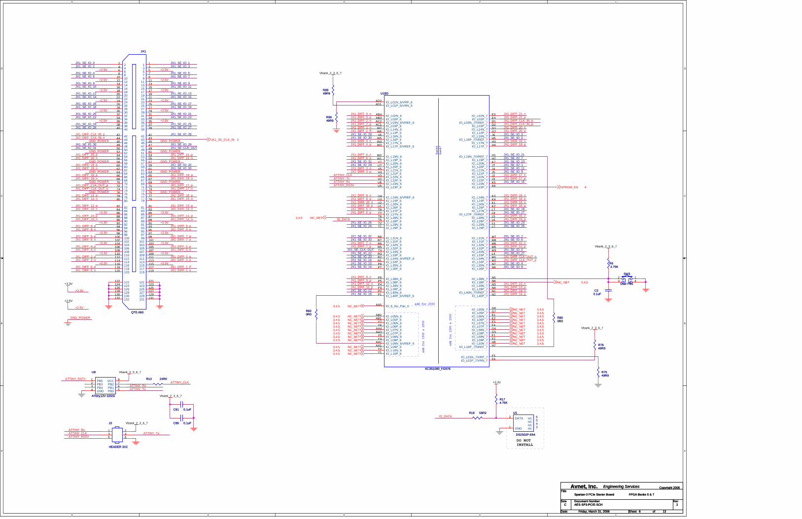
5
5
4
4
3
3
2
2
1
1
D D
C C
B B
A A
JX1_SE_IO_21
JX1_SE_IO_18
+2.5V
+3.3V
GND_POWER
+3.3V
+3.3V
+3.3V
+3.3V
+3.3V
+3.3V
GND_POWER
GND_POWER
GND_POWER
GND_POWER
GND_POWER
GND_POWER
+2.5V
+2.5V
+2.5V
+2.5V
+2.5V
+2.5V
+2.5V
+2.5V
+2.5V
+2.5V
+2.5V
+2.5V
GND_POWER
GND_POWER
GND_POWER
GND_POWER
GND_POWER
GND_POWER
+3.3V
+3.3V
+3.3V
+3.3V
+3.3V
+3.3V
ATTINY_RST#
ATTINY_RxATTINY_Tx
ATTINY_CLK
ATTINY_RxATTINY_CLKATTINY_RST#
ATTINY_Tx
JX1_DIFF_0_nJX1_DIFF_0_p
JX1_SE_IO_12
JX1_DIFF_CLK_IN_nJX1_DIFF_CLK_IN_p
JX1_DIFF_12_p
JX1_DIFF_18_nJX1_DIFF_18_pJX1_DIFF_16_nJX1_DIFF_16_p
JX1_DIFF_CLK_OUT_nJX1_DIFF_CLK_OUT_p
JX1_DIFF_14_nJX1_DIFF_14_p
JX1_DIFF_12_n
JX1_DIFF_10_nJX1_DIFF_10_p
JX1_DIFF_8_nJX1_DIFF_8_p
JX1_DIFF_6_nJX1_DIFF_6_p
JX1_DIFF_4_nJX1_DIFF_4_p
JX1_DIFF_2_nJX1_DIFF_2_p
JX1_DIFF_20_nJX1_DIFF_20_p
JX1_SE_IO_30
JX1_SE_IO_31
JX1_SE_IO_20JX1_SE_IO_22
JX1_SE_IO_24JX1_SE_IO_26
JX1_SE_IO_8
JX1_SE_IO_0
JX1_SE_IO_2
JX1_SE_IO_4
JX1_SE_IO_6
JX1_SE_IO_10JX1_SE_IO_14
JX1_SE_IO_16
ATTINY_RST#ATTINY_RxATTINY_TxATTINY_CLK
JX1_DIFF_11_nJX1_DIFF_11_p
JX1_DIFF_9_nJX1_DIFF_9_p
JX1_DIFF_7_nJX1_DIFF_7_p
JX1_DIFF_5_nJX1_DIFF_5_p
JX1_DIFF_3_nJX1_DIFF_3_p
JX1_DIFF_1_nJX1_DIFF_1_P
JX1_DIFF_21_nJX1_DIFF_21_p
JX1_DIFF_19_nJX1_DIFF_19_p
JX1_DIFF_17_nJX1_DIFF_17_p
JX1_DIFF_15_nJX1_DIFF_15_p
JX1_DIFF_13_p
JX1_SE_IO_23JX1_SE_IO_25
JX1_SE_IO_27
JX1_SE_IO_28
JX1_SE_IO_29
JX1_SE_CLK_OUT
JX1_DIFF_13_n
JX1_SE_IO_32JX1_SE_IO_33
JX1_SE_IO_3
JX1_SE_IO_1
JX1_SE_IO_5
JX1_SE_IO_11
JX1_SE_IO_13
JX1_SE_IO_15
JX1_SE_IO_17JX1_SE_IO_19
JX1_SE_IO_7
JX1_SE_IO_9
ID_DATA
ID_DATA
JX1_SE_IO_1JX1_SE_IO_3
JX1_SE_IO_5JX1_SE_IO_7
JX1_SE_IO_9JX1_SE_IO_11
JX1_SE_IO_13JX1_SE_IO_15
JX1_SE_IO_17JX1_SE_IO_19
JX1_SE_IO_21JX1_SE_IO_23
JX1_SE_IO_25JX1_SE_IO_27
JX1_SE_IO_28
JX1_SE_IO_29JX1_SE_CLK_OUT
JX1_DIFF_21_pJX1_DIFF_21_n
JX1_SE_IO_32JX1_SE_IO_33
JX1_DIFF_19_pJX1_DIFF_19_n
JX1_DIFF_17_pJX1_DIFF_17_n
JX1_DIFF_15_pJX1_DIFF_15_n
JX1_DIFF_13_pJX1_DIFF_13_n
JX1_DIFF_11_pJX1_DIFF_11_n
JX1_DIFF_9_pJX1_DIFF_9_n
JX1_DIFF_7_pJX1_DIFF_7_n
JX1_DIFF_5_pJX1_DIFF_5_n
JX1_DIFF_3_pJX1_DIFF_3_n
JX1_SE_IO_0JX1_SE_IO_2
JX1_SE_IO_4JX1_SE_IO_6
JX1_SE_IO_8JX1_SE_IO_10
JX1_SE_IO_12JX1_SE_IO_14
JX1_SE_IO_16JX1_SE_IO_18
JX1_SE_IO_20JX1_SE_IO_22
JX1_SE_IO_24JX1_SE_IO_26
JX1_DIFF_CLK_IN_pJX1_DIFF_CLK_IN_n
JX1_SE_IO_30JX1_SE_IO_31
JX1_DIFF_20_pJX1_DIFF_20_n
JX1_DIFF_18_pJX1_DIFF_18_n
JX1_DIFF_16_pJX1_DIFF_16_n
JX1_DIFF_CLK_OUT_pJX1_DIFF_CLK_OUT_n
JX1_DIFF_14_pJX1_DIFF_14_n
JX1_DIFF_12_pJX1_DIFF_12_n
JX1_DIFF_10_pJX1_DIFF_10_n
JX1_DIFF_8_pJX1_DIFF_8_n
JX1_DIFF_6_pJX1_DIFF_6_n
JX1_DIFF_4_pJX1_DIFF_4_n
JX1_DIFF_2_pJX1_DIFF_2_n
JX1_DIFF_0_pJX1_DIFF_0_n
JX1_DIFF_1_PJX1_DIFF_1_n
+3.3V
+2.5V
Vbank_2_3_6_7
Vbank_2_3_6_7
Vbank_2_3_6_7
Vbank_2_3_6_7
Vbank_2_3_6_7
Vbank_2_3_6_7
+3.3V
NC_NET3,4,5NC_NET3,4,5
NC_NET3,4,5NC_NET3,4,5NC_NET3,4,5NC_NET3,4,5NC_NET3,4,5NC_NET3,4,5NC_NET3,4,5NC_NET3,4,5
NC_NET3,4,5
NC_NET 3,4,5NC_NET 3,4,5NC_NET 3,4,5NC_NET 3,4,5NC_NET 3,4,5NC_NET 3,4,5NC_NET 3,4,5NC_NET 3,4,5NC_NET 3,4,5NC_NET 3,4,5NC_NET 3,4,5
NC_NET3,4,5
NC_NET 3,4,5
JX1_SE_CLK_IN 3
SPROM_EN 4
NC_NET3,4,5
Title
Size Document Number Rev
Date: Sheet of
Avnet, Inc. Engineering Services Copyright 2006
AES-SP3-PCIE-SCH 2
Spartan-3 PCIe Starter Board
C
6Friday, March 31, 2006 13
FPGA Banks 6 & 7Title
Size Document Number Rev
Date: Sheet of
Avnet, Inc. Engineering Services Copyright 2006
AES-SP3-PCIE-SCH 2
Spartan-3 PCIe Starter Board
C
6Friday, March 31, 2006 13
FPGA Banks 6 & 7Title
Size Document Number Rev
Date: Sheet of
Avnet, Inc. Engineering Services Copyright 2006
AES-SP3-PCIE-SCH 2
Spartan-3 PCIe Starter Board
C
6Friday, March 31, 2006 13
FPGA Banks 6 & 7
DO NOTINSTALL
U8
ATtiny13V-10SSI
U8
ATtiny13V-10SSI
PB51PB32PB43GND4 PB0 5PB1 6PB2 7VCC 8
J3
HEADER 3X2
J3
HEADER 3X2
246
135
bank6
bank7
add for 1500 & 2000
add for 1500 & 2000
add for 2000
U18D
XC3S1000_FG676
bank6
bank7
add for 1500 & 2000
add for 1500 & 2000
add for 2000
U18D
XC3S1000_FG676
IO_6_No_Pair_0AA5
IO_L01N_6/VRP_6AD2IO_L01P_6/VRN_6AD1
IO_L02N_6AB4IO_L02P_6AB3IO_L03N_6/VREF_6AC2IO_L03P_6AC1
IO_L05N_6AB2IO_L05P_6AB1IO_L06N_6Y7IO_L06P_6Y6IO_L07N_6AA4IO_L07P_6AA3IO_L08N_6Y5IO_L08P_6Y4IO_L09N_6/VREF_6AA2IO_L09P_6AA1IO_L10N_6Y2IO_L10P_6Y1
IO_L14N_6W7IO_L14P_6W6IO_L16N_6V6IO_L16P_6W5IO_L17N_6W4IO_L17P_6/VREF_6W3
IO_L19N_6W2IO_L19P_6W1IO_L20N_6V7IO_L20P_6U7IO_L21N_6V5IO_L21P_6V4IO_L22N_6V3IO_L22P_6V2
IO_L24N_6/VREF_6U4IO_L24P_6U3IO_L26N_6U2IO_L26P_6U1
IO_L27N_6T7 IO_L27P_6T8
IO_L28N_6T6IO_L28P_6T5IO_L29N_6T2IO_L29P_6T1
IO_L31N_6R8IO_L31P_6R7IO_L32N_6R6IO_L32P_6R5IO_L33N_6T4IO_L33P_6R3IO_L34N_6/VREF_6R2IO_L34P_6R1IO_L35N_6P8IO_L35P_6P7
IO_L38N_6P6IO_L38P_6P5IO_L39N_6P4IO_L39P_6P3IO_L40N_6P2IO_L40P_6/VREF_6P1
IO_L01N_7/VRP_7 F5IO_L01P_7/VRN_7 F6
IO_L02N_7 E3IO_L02P_7 E4
IO_L03N_7/VREF_7 D1IO_L03P_7 D2
IO_L05N_7 G6IO_L05P_7 G7IO_L06N_7 E1IO_L06P_7 E2IO_L07N_7 F3IO_L07P_7 F4IO_L08N_7 G4IO_L08P_7 G5IO_L09N_7 F1IO_L09P_7 F2IO_L10N_7 H6
IO_L10P_7/VREF_7 H7
IO_L14N_7 G1IO_L14P_7 G2IO_L16N_7 J6
IO_L16P_7/VREF_7 H5IO_L17N_7 H3IO_L17P_7 H4
IO_L19N_7/VREF_7 H1IO_L19P_7 H2IO_L20N_7 K7IO_L20P_7 J7IO_L21N_7 J4IO_L21P_7 J5IO_L22N_7 J2IO_L22P_7 J3IO_L23N_7 K5IO_L23P_7 K6
IO_L24N_7 K3IO_L24P_7 K4IO_L26N_7 K1IO_L26P_7 K2IO_L27N_7 L7
IO_L27P_7/VREF_7 L8IO_L28N_7 L5IO_L28P_7 L6IO_L29N_7 L1IO_L29P_7 L2
IO_L31N_7 M7IO_L31P_7 M8IO_L32N_7 M6IO_L32P_7 M5IO_L33N_7 M3IO_L33P_7 L4IO_L34N_7 M1IO_L34P_7 M2IO_L35N_7 N7IO_L35P_7 N8
IO_L38N_7 N5IO_L38P_7 N6IO_L39N_7 N3IO_L39P_7 N4
IO_L40N_7/VREF_7 N1IO_L40P_7 N2
IO_L23N_6U6IO_L23P_6U5
C91 0.1uFC91 0.1uF
R13 24R0R13 24R0
R800R0R800R0
C96 0.1uFC96 0.1uF
R820R0R820R0
R7549R9R7549R9
U5
DS2502P-E64
U5
DS2502P-E64
GND1
DATA2
n/c 3n/c 4n/c 5n/c 6
R7649R9R7649R9
SW3
User PB1
SW3
User PB13
14
2
R18 56R2R18 56R2
R8949R9R8949R9
R174.75KR174.75K
R9049R9R9049R9
R64.75K
R64.75K
JX1
QTE-060
JX1
QTE-060
224466881010121214141616181820202222242426262828303032323434363638384040
42424444464648485050525254545656585860606262646466666868707072727474767678788080
828284848686888890909292949496969898100100102102104104106106108108110110112112114114116116118118120120
122122124124126126128128130130132132
1 13 35 57 79 9
11 1113 1315 1517 1719 1921 2123 2325 2527 2729 2931 3133 3335 3537 3739 39
41 4143 4345 4547 4749 4951 5153 5355 5557 5759 5961 6163 6365 6567 6769 6971 7173 7375 7577 7779 79
81 8183 8385 8587 8789 8991 9193 9395 9597 9799 99
101 101103 103105 105107 107109 109111 111113 113115 115117 117119 119
121 121123 123125 125127 127129 129131 131
C30.1uFC3
0.1uF

5
5
4
4
3
3
2
2
1
1
D D
C C
B B
A A
+1.2V +2.5V
+2.5V
+3.3V +2.5V
+1.2V
+2.5V
Vbank_2_3_6_7
+2.5V
Vbank_2_3_6_7Vbank_2_3_6_7
Vbank_2_3_6_7
+1.25V_REF +1.25V_TT
Title
Size Document Number Rev
Date: Sheet of
Avnet, Inc. Engineering Services Copyright 2006
AES-SP3-PCIE-SCH 2
Spartan-3 PCIe Starter Board
C
7Friday, March 31, 2006 13
FPGA PowerTitle
Size Document Number Rev
Date: Sheet of
Avnet, Inc. Engineering Services Copyright 2006
AES-SP3-PCIE-SCH 2
Spartan-3 PCIe Starter Board
C
7Friday, March 31, 2006 13
FPGA PowerTitle
Size Document Number Rev
Date: Sheet of
Avnet, Inc. Engineering Services Copyright 2006
AES-SP3-PCIE-SCH 2
Spartan-3 PCIe Starter Board
C
7Friday, March 31, 2006 13
FPGA Power
CAP 0201 CAP 0402 CAP 0603
CAP 0201 CAP 0402 CAP 0603
CAP 0201 CAP 0402 CAP 0603
CAP TAN-D
CAP TAN-D
CAP TAN-D
CAP 0201CAP 0201 CAP 0402 CAP 0402
C212
4.7uF
C212
4.7uF
C185
0.01uF
C185
0.01uF
C106
0.01uF
C106
0.01uF
C186
0.01uF
C186
0.01uF
C164
0.01uF
C164
0.01uF
C153
0.01uF
C153
0.01uF
C101
0.01uF
C101
0.01uF
C184
0.01uF
C184
0.01uF
C49
4.7uF
C49
4.7uF
C51
1.0uF
C51
1.0uF
C181
1.0uF
C181
1.0uF
C47
1.0uF
C47
1.0uF
C12
4.7uF
C12
4.7uF
C36
4.7uF
C36
4.7uF
C167
0.01uF
C167
0.01uF
C102
0.01uF
C102
0.01uF
C23
1.0uF
C23
1.0uF
C35
4.7uF
C35
4.7uF
C168
0.01uF
C168
0.01uF
C123
0.01uF
C123
0.01uF
C165
0.01uF
C165
0.01uF
C150
1.0uF
C150
1.0uF
C125
0.01uF
C125
0.01uF
C155
0.01uF
C155
0.01uF
C166
0.01uF
C166
0.01uF
C22
1.0uF
C22
1.0uF
C117
0.01uF
C117
0.01uF
+C40470uF
+C40470uF
12
C92
1.0uF
C92
1.0uF
C130
0.01uF
C130
0.01uF
C131
0.01uF
C131
0.01uF
C17
1.0uF
C17
1.0uF
C129
1.0uF
C129
1.0uF
C151
1.0uF
C151
1.0uF
C99
1.0uF
C99
1.0uF
C77
1.0uF
C77
1.0uF
C118
0.01uF
C118
0.01uF
C103
0.01uF
C103
0.01uF
C105
0.01uF
C105
0.01uF
C172
0.01uF
C172
0.01uF
C110
0.01uF
C110
0.01uF
C154
0.01uF
C154
0.01uF
C50
1.0uF
C50
1.0uF
C182
0.01uF
C182
0.01uF
C119
0.01uF
C119
0.01uF
C104
0.01uF
C104
0.01uF
C149
0.01uF
C149
0.01uF
C19
4.7uF
C19
4.7uF
C20
1.0uF
C20
1.0uF
C112
1.0uF
C112
1.0uF
C127
0.01uF
C127
0.01uF
C25
4.7uF
C25
4.7uF
C107
0.01uF
C107
0.01uF
C124
0.01uF
C124
0.01uF
C113
1.0uF
C113
1.0uF
C173
4.7uF
C173
4.7uF
C141
0.01uF
C141
0.01uF
C41
1.0uF
C41
1.0uF
C157
0.01uF
C157
0.01uF
C132
0.01uF
C132
0.01uF
C108
0.01uF
C108
0.01uF
C78
1.0uF
C78
1.0uF
C146
4.7uF
C146
4.7uF
C90
1.0uF
C90
1.0uF
U18F
XC3S1000_FG676
U18F
XC3S1000_FG676
VCCAUX A2VCCAUX A9VCCAUX A18VCCAUX A25VCCAUX B1VCCAUX B26VCCAUX J1VCCAUX J26VCCAUX V1VCCAUX V26
VCCAUX AE1VCCAUX AE26VCCAUX AF2VCCAUX AF9VCCAUX AF18VCCAUX AF25
VCCINTH8VCCINTH19VCCINTJ9VCCINTJ10VCCINTJ17VCCINTJ18VCCINTK9VCCINTK10VCCINTK17VCCINTK18
VCCINTU9VCCINTU10VCCINTU17VCCINTU18VCCINTV9VCCINTV10VCCINTV17VCCINTV18VCCINTW8VCCINTW19
C145
1.0uF
C145
1.0uF
C133
0.01uF
C133
0.01uF
C76
1.0uF
C76
1.0uF
+C39470uF
+C39470uF
12
C26
4.7uF
C26
4.7uF
C183
0.01uF
C183
0.01uF
C48
1.0uF
C48
1.0uF
C143
0.01uF
C143
0.01uF
C95
0.01uF
C95
0.01uF
C160
0.01uF
C160
0.01uF
C177
0.01uF
C177
0.01uF
C170
0.01uF
C170
0.01uF
C134
0.01uF
C134
0.01uF
C161
0.01uF
C161
0.01uF
C152
1.0uF
C152
1.0uF
C156
0.01uF
C156
0.01uF
C140
0.01uF
C140
0.01uF
C115
0.01uF
C115
0.01uF
C135
0.01uF
C135
0.01uF
C139
1.0uF
C139
1.0uF
C158
0.01uF
C158
0.01uF
C120
0.01uF
C120
0.01uF
JP5
Bank 2, 3, 6, 7 VCCO Select
JP5
Bank 2, 3, 6, 7 VCCO Select
1 3
2
C126
1.0uF
C126
1.0uF
C178
0.01uF
C178
0.01uF
C42
1.0uF
C42
1.0uF
C162
1.0uF
C162
1.0uF
C137
0.01uF
C137
0.01uF
C138
1.0uF
C138
1.0uF
C128
0.01uF
C128
0.01uF
C175
0.01uF
C175
0.01uF
C142
0.01uF
C142
0.01uF
C30
1.0uF
C30
1.0uF
C21
4.7uF
C21
4.7uF
bank0
bank4
bank1
bank5
bank2
bank6
bank3
bank7
U18E
XC3S1000_FG676
bank0
bank4
bank1
bank5
bank2
bank6
bank3
bank7
U18E
XC3S1000_FG676
VCCO_0C7VCCO_0C11VCCO_0H9VCCO_0H10VCCO_0J11VCCO_0J12VCCO_0J13VCCO_0K13
VCCO_1C16VCCO_1C20VCCO_1H17VCCO_1H18VCCO_1J14VCCO_1J15VCCO_1J16VCCO_1K14
VCCO_2G24VCCO_2J19VCCO_2K19VCCO_2L18VCCO_2L24VCCO_2M18VCCO_2N17VCCO_2N18
VCCO_3P17VCCO_3P18VCCO_3R18VCCO_3T18VCCO_3T24VCCO_3U19VCCO_3V19VCCO_3Y24
VCCO_4 U14VCCO_4 V14VCCO_4 V15VCCO_4 V16VCCO_4 W17VCCO_4 W18VCCO_4 AD16VCCO_4 AD20
VCCO_5 U13VCCO_5 V11VCCO_5 V12VCCO_5 V13VCCO_5 W9VCCO_5 W10VCCO_5 AD7VCCO_5 AD11
VCCO_6 P9VCCO_6 P10VCCO_6 R9VCCO_6 T3VCCO_6 T9VCCO_6 U8VCCO_6 V8VCCO_6 Y3
VCCO_7 G3VCCO_7 J8VCCO_7 K8VCCO_7 L3VCCO_7 L9VCCO_7 M9VCCO_7 N9VCCO_7 N10
C144
1.0uF
C144
1.0uF
C114
4.7uF
C114
4.7uF
C18
1.0uF
C18
1.0uF
+C52470uF
+C52470uF
12
C88
1.0uF
C88
1.0uF
C93
1.0uF
C93
1.0uF
C163
0.01uF
C163
0.01uF
C136
0.01uF
C136
0.01uF
C176
0.01uF
C176
0.01uF
C122
4.7uF
C122
4.7uF
+C24470uF
+C24470uF
12
C75
1.0uF
C75
1.0uF
U18G
XC3S1000_FG676
U18G
XC3S1000_FG676
GNDA1GNDA26GNDB2GNDB25GNDC3GNDC24GNDD4GNDD12GNDD15GNDD23
GNDK11GNDK12GNDK15GNDK16GNDL10GNDL11GNDL12GNDL13GNDL14GNDL15
GNDL16GNDL17GNDM4GNDM10GNDM11GNDM12GNDM13GNDM14GNDM15GNDM16
GNDM17GNDM23GNDN11GNDN12GNDN13GNDN14GNDN15GNDN16
GND P11GND P12GND P13GND P14GND P15GND P16GND R4GND R10GND R11GND R12
GND R13GND R14GND R15GND R16GND R17GND R23GND T10GND T11GND T12GND T13
GND T14GND T15GND T16GND T17GND U11GND U12GND U15GND U16GND AC4GND AC12
GND AC15GND AC23GND AD3GND AD24GND AE2GND AE25GND AF1GND AF26
C111
0.01uF
C111
0.01uF
C89
1.0uF
C89
1.0uF
C29
1.0uF
C29
1.0uF

5
5
4
4
3
3
2
2
1
1
D D
C C
B B
A A
FPGA_DONE
FPGA_PROG#
FPGA_D0FPGA_D1FPGA_D2FPGA_D3FPGA_D4FPGA_D5FPGA_D6FPGA_D7
FPGA_CCLK
FPGA_CCLK
PROM_CE#
JTAG_TMSJTAG_TCK
PROM_TDI
PROM_TDO
JTAG_TMS
FPGA_TDIFPGA_TDO
PROM_TDIJTAG_TDOJTAG_TCK
FPGA_TDI
FPGA_DONE
JTAG_TDI
JTAG_TMS
PROM_TDO
FPGA_DONEPROM_CE#
JTAG_TCK
FPGA_CCLK
PROM_CE#
FPGA_PROG#
FPGA_PROG#
PROM_TDO
FPGA_TDO
+3.3V
+2.5V+1.8V
+2.5V
+2.5V
+2.5V
+2.5V
+2.5V
+2.5V
+2.5V+2.5V
+2.5V
+3.3V
+2.5V
+2.5V
+2.5V
+2.5V
+2.5V
+2.5V
+2.5V
+2.5V
+2.5V
+2.5V
+2.5V
+2.5V
+2.5V
FPGA_BUSY# 5FPGA_INIT#5
FPGA_D05FPGA_D15FPGA_D25FPGA_D35FPGA_D45FPGA_D55FPGA_D65FPGA_D75
FPGA_to_PROM5
FPGA_TDI_to_PROM5
FPGA_TCK_to_PROM5
FPGA_TMS_to_PROM5
PROM_TDO_to_FPGA5
FPGA_PROM_READ4
FPGA_to_PROM_CCLK4
FPGA_to_PROM_CE#4
PO_RESET# 12
Title
Size Document Number Rev
Date: Sheet of
Avnet, Inc. Engineering Services Copyright 2006
AES-SP3-PCIE-SCH 2
Spartan-3 PCIe Starter Board
C
8Friday, March 31, 2006 13
FPGA ConfigurationTitle
Size Document Number Rev
Date: Sheet of
Avnet, Inc. Engineering Services Copyright 2006
AES-SP3-PCIE-SCH 2
Spartan-3 PCIe Starter Board
C
8Friday, March 31, 2006 13
FPGA ConfigurationTitle
Size Document Number Rev
Date: Sheet of
Avnet, Inc. Engineering Services Copyright 2006
AES-SP3-PCIE-SCH 2
Spartan-3 PCIe Starter Board
C
8Friday, March 31, 2006 13
FPGA Configuration
JTAG Parallel IV Connector
Jumper J4 for normal operation (default)
Remove J4 jumper to allow FPGA toaccess Config PROM for data storage
DNI
JP1/JP2 Settings:PROM and FPGA in chain - JP2 2:3, JP1 2:3PROM only in chain - JP2 2:3, JP1 1:2FPGA only in chain - JP2 1:2, JP1 2:3
Configuration Mode M0 (JP3 5:6) M1 (JP3 3:4) M2 (JP3 1:2)
Master Serial
Slave Serial
Master Parallel
Slave Parallel
JTAG
0 0 0
1 1 1
1 1
1 1
11
0
0
0
Note: With no shunts installed on JP3, M0 = M1 = M2 = 1 via RP28
R46 1KR46 1K
C190 0.1uFC190 0.1uF
U18H
XC3S1000_FG676
U18H
XC3S1000_FG676
CCLK AD26PROG_B D3
DONE AC24
M0 AE3M1 AC3M2 AF3
HSWAP_EN C2
TCKB24TDIC1TDOD24TMSA24
U29
NC7SV126
U29
NC7SV126
2 45
1
3
C193 0.1uFC193 0.1uF
JP10
HEADER 2
JP10
HEADER 2
12
JP7
HEADER 2
JP7
HEADER 2
12
R484.75KR484.75K
RP29 1KRP29 1K18273645
U41
NC7SV126
U41
NC7SV126
2 45
1
3
C171 0.1uFC171 0.1uFJP1
JUMPER_2WAYJP1
JUMPER_2WAY1 3
2
JP3
HEADER 3X2
JP3
HEADER 3X2
246
135
C187 0.1uFC187 0.1uF
J4
HEA
DER
2
J4
HEA
DER
2
12
JP4
HEADER 3X2
JP4
HEADER 3X2
246
135
JP2JUMPER_2WAY
JP2JUMPER_2WAY
1 3
2
R55330R55330
U27
NC7SV126
U27
NC7SV126
2 45
1
3
RP28 1KRP28 1K18273645
C198 0.1uFC198 0.1uF
R514.75KR514.75K
U44
NC7SV126
U44
NC7SV126
2 45
1
3
R214.75KR214.75K
U24
XCFxxP - VO48
U24
XCFxxP - VO48
CLK12OE/RST11CE13
GN
D2
VC
CO
8
VC
C_I
NT
4V
CC
_IN
T15
D028D129D232D333D443D544D647D748
CEO 10
GN
D7
GN
D17
GN
D23
VC
C_I
NT
34
VC
CO
30V
CC
O38
VC
CO
45
CF 6
TDI19
TCK20TMS21 TDO 22
EN_EXT_SEL 25REV_SEL0 26REV_SEL1 27
BUSY 5CLKOUT 9
VC
CJ
24
GN
D31
GN
D36
GN
D46
NC40NC41NC42
NC
1N
C3
NC
14N
C16
NC
18
NC
39N
C37
NC
35
R5010KR5010K
R106
100
R106
100
J2
87832-1420
J2
87832-1420
NC 14GND13NC 12GND11TDI 10GND9
TDO 8GND7TCK 6GND5TMS 4GND3
VREF 2GND1
U45
NC7SV126
U45
NC7SV126
245
1
3
R105
100
R105
100
D14
DONE
D14
DONE
C192 0.1uFC192 0.1uF
U38
74V1G04
U38
74V1G04
2 4
5
3
U42
NC7SV126
U42
NC7SV126
2 45
1
3
R494.75K
R494.75K
R201KR201K
R47 680R47 680

5
5
4
4
3
3
2
2
1
1
D D
C C
B B
A A
PCIe_Tx_D0PCIe_Tx_D1PCIe_Tx_D2PCIe_Tx_D3PCIe_Tx_D4PCIe_Tx_D5PCIe_Tx_D6PCIe_Tx_D7
PCIe_TDIPCIe_TDOPCIe_TCKPCIe_TMS
PCIe_REF_CLKn
PCIe_REF_CLKp
PCIe_Rx_D0PCIe_Rx_D1PCIe_Rx_D2PCIe_Rx_D3
PCIe_Rx_D4PCIe_Rx_D5PCIe_Rx_D6PCIe_Rx_D7
PCIe_RXn
PCIe_RXp
PCIe_RXpPCIe_RXn
PCIe_TDIPCIe_TDO
PCIe_REF_CLKpPCIe_REF_CLKn
PCIe_PERST#
PCIe_PRSNT#
PCIe_PRSNT#
PCIe_SMCLK
PCIe_SMDAT
PCIe_WAKE#
PCIe_Tx_EIDLEPCIe_Tx_COMPPCIe_Tx_DATAKPCIe_Tx_DET_LOOP
PCIe_Tx_D0PCIe_Tx_D1PCIe_Tx_D2PCIe_Tx_D3
PCIe_Tx_D4PCIe_Tx_D5PCIe_Tx_D6PCIe_Tx_D7
PCIe_Rx_POLARPCIe_Tx_CLK
PCIe_PERST#
PCIe_TXn
PCIe_TXp
PCIe_TXn
PCIe_TXp
PCIe_PERST#
PCIe_TRST#PCIe_TMS
PCIe_TCK
PCIe_TRST#
+2.5V
+3.3V
+3.3V
+3.3V
+2.5V
+1.2V
+2.5V
+1.25V_TT
+3.3V
+2.5V
+1.25V_PHY+2.5V
+1.25V_PHY
+1.25V_TT
+1.25V_PHY
+1.25V_PHY
PCIe_Tx_D[0:7]5
PCIe_Rx_DATAK5PCIe_Rx_VALID5
PCIe_Rx_CLK5
PCIe_Rx_STAT05PCIe_Rx_STAT15PCIe_Rx_STAT25
PCIe_Rx_EIDLE5
PCIe_Rx_POLAR5
PCIe_Tx_DATAK5PCIe_Tx_CLK5PCIe_Tx_EIDLE5PCIe_Tx_COMP5
PCIe_Tx_DET_LOOP5
PCIe_Rx_D[0:7]5
FPGA_PHY_RESET#5
PCIe_RESET#5
PCIe_PWRDN05PCIe_PWRDN15
PCIe_PHY_STAT5
Title
Size Document Number Rev
Date: Sheet of
Avnet, Inc. Engineering Services Copyright 2006
AES-SP3-PCIE-SCH 2
Spartan-3 PCIe Starter Board
C
9Friday, March 31, 2006 13
PCI ExpressTitle
Size Document Number Rev
Date: Sheet of
Avnet, Inc. Engineering Services Copyright 2006
AES-SP3-PCIE-SCH 2
Spartan-3 PCIe Starter Board
C
9Friday, March 31, 2006 13
PCI ExpressTitle
Size Document Number Rev
Date: Sheet of
Avnet, Inc. Engineering Services Copyright 2006
AES-SP3-PCIE-SCH 2
Spartan-3 PCIe Starter Board
C
9Friday, March 31, 2006 13
PCI Express
Place RP24 - RP26, RP48 - RP52, R101 close to U35
To supply power from PCIe, fuse MUST be infuseholder F2 and NOT in fuseholder F1 (Powerconnector J1/J5)
C59 0.1uFC59 0.1uF
RP25 49R9RP25 49R91 82 73 64 5
TP4TP4
C56
0.1uF
C56
0.1uF
C218 0.1uFC218 0.1uF
C57
0.1uF
C57
0.1uF
C217 0.1uFC217 0.1uF
C61
0.1uF
C61
0.1uF
FB3
FER
RIT
E BE
ADFB
3FE
RR
ITE
BEAD
11
22
RP52 24R0RP52 24R018273645
C222 0.1uFC222 0.1uF
TP3TP3
R56 49R9R56 49R9
R101 24R0R101 24R0
+C64
10uF
+C64
10uF
12
C73 0.1uFC73 0.1uF
TP2TP2
RP50 24R0RP50 24R018273645
C204
0.1uF
C204
0.1uF
RP26 49R9RP26 49R91 82 73 64 5
+ C63
10uF
+ C63
10uF
12
C72 0.1uFC72 0.1uF
F2
FUSEHOLDER
F2
FUSEHOLDER
FB1
FER
RIT
E BE
ADFB
1FE
RR
ITE
BEAD
11
22
C216
0.1uF
C216
0.1uF
C208
0.1uF
C208
0.1uF
R53DNIR53DNI
U35
PX1011A
U35
PX1011A
VS
SA
1
Rx_EIDLEA2
Rx_D6A3
Rx_D4A4 Rx_D3A5
Rx_D1A6
Rx_DATAKA7
Rx_CLKA8
Rx_STAT0A9
RE
F_C
LKp
B1
VS
SB
2
Rx_D7B3
Rx_D5B4
VS
SB
5
Rx_D2B6
Rx_D0B7
VS
SB
8
Rx_STAT1B9
VS
SD
1V
SS
D2
VD
D4
D3
VD
D_A
2D
4
VD
D_A
1D
5
PV
TD
6
VS
SD
7
PHY_STATD8
Tx_D0D9
RXp E1
VS
SE
2
VD
D1
E3
TMS E4
VD
D1
E5
VD
D3
E6
VD
D2
E7
VS
SE
8
Tx_D1E9
RE
F_C
LKn
C1
VS
SC
2
VD
D2
C3
VS
SC
4
VD
D2
C5
VS
SC
6
VD
D2
C7
Rx_VALIDC8
Rx_STAT2C9
RXn F1
VS
SF2
TCK F3
TRST# F4
VD
D3
F5V
DD
3F6
VS
SF7
Tx_D3F8 Tx_D2F9
VS
SG
1V
SS
G2
TDI G3
VS
SG
4V
DD
2G
5V
SS
G6
VD
D2
G7
Tx_D5G8 Tx_D4G9 TXp H1
VS
SH
2
TDO H3
Tx_EIDLEH4
VS
SH
5
PWR_DN0H6
Tx_DET_LOOPH7
VS
SH
8
Tx_D6H9
TXn J1
Vre
f_S
STL
J2
RESETnJ3
Rx_POLARJ4
Tx_COMPJ5
PWR_DN1J6
Tx_DATAKJ7Tx_CLKJ8
Tx_D7J9
C55
0.1uF
C55
0.1uF
C210
0.1uF
C210
0.1uF
C206
0.1uF
C206
0.1uF
C74 0.1uFC74 0.1uF
C62
0.1uF
C62
0.1uF
C670.1uF C670.1uF
Mechanical Key
1x
Note: Pin names are from the add-in board perspective
P3
PCI_Express_x1
Mechanical Key
1x
Note: Pin names are from the add-in board perspective
P3
PCI_Express_x1
+12VB1+12VB2RSVDB3GNDB4SMCLKB5SMDATB6GNDB7+3.3VB8TRST#B93.3VauxB10WAKE#B11
PERp0B14PERn0B15GNDB16PRSNT2#B17GNDB18
REFCLK_N A14GND A15
PETp0 A16PETn0 A17
GND A18
PRSNT1# A1+12V A2+12V A3GND A4TCK A5TDI A6
TDO A7TMS A8
+3.3V A9+3.3V A10
PERST# A11
RSVDB12GNDB13 GND A12
REFCLK_P A13
C71 0.1uFC71 0.1uF
RP49 49R9RP49 49R91 82 73 64 5
C211
0.1uF
C211
0.1uF
C207
0.1uF
C207
0.1uF
R1111K
R1111K
R109330R109330
C223 0.1uFC223 0.1uF
C221 0.1uFC221 0.1uF
RP51 49R9RP51 49R91 82 73 64 5
U32TPS736125DRB
U32TPS736125DRB
OUT 1
N/C 2
NR/FB 3
GND4
EN5
N/C 6N/C 7
IN8
Pad9
FB2
FER
RIT
E BE
ADFB
2FE
RR
ITE
BEAD
11
22
R104DNIR104DNI
RP24 24R0RP24 24R018273645
C220 0.1uFC220 0.1uF
C209
0.1uF
C209
0.1uF
C60
0.1uF
C60
0.1uF
C215
0.1uF
C215
0.1uF
R102560R102560
+
C70 47uF
+
C70 47uF1 2
R103560R103560
C219 0.1uFC219 0.1uF
RP48 24R0RP48 24R018273645

5
5
4
4
3
3
2
2
1
1
D D
C C
B B
A A
DDR_D12DDR_D13DDR_D14DDR_D15
MEM_D[0:31]
MEM_D12MEM_D13MEM_D14MEM_D15
MEM_D0MEM_D1MEM_D2MEM_D3
MEM_D4MEM_D5MEM_D6MEM_D7
MEM_D8MEM_D9MEM_D10MEM_D11
DDR_D0DDR_D1DDR_D2DDR_D3
DDR_D4DDR_D5DDR_D6DDR_D7
DDR_D8DDR_D9DDR_D10DDR_D11
MEM_D7
MEM_D3
MEM_D0MEM_D1MEM_D2
MEM_D11
MEM_D8MEM_D9MEM_D10
MEM_D15
MEM_D12MEM_D13MEM_D14
MEM_D4MEM_D5MEM_D6
MEM_D0MEM_D1MEM_D2MEM_D3DDR_DQS1_TermMEM_D4MEM_D5
MEM_D[0:31]
MEM_D6MEM_D7MEM_D8MEM_D9MEM_D10MEM_D11MEM_D12
DDR_DQS0_Term
MEM_D13MEM_D14
DDR_A0DDR_A1DDR_A2DDR_A3
DDR_A4DDR_A5DDR_A6DDR_A7
DDR_A11DDR_A9
DDR_A8
DDR_A10
MEM_D15
DDR_A0DDR_A1DDR_A2DDR_A3DDR_A4DDR_A5DDR_A6DDR_A7DDR_A8DDR_A9DDR_A10DDR_A11DDR_A12
MEM_D16MEM_D17MEM_D18MEM_D19MEM_D20MEM_D21MEM_D22MEM_D23MEM_D24MEM_D25MEM_D26MEM_D27MEM_D28MEM_D29MEM_D30MEM_D31
DDR_A0DDR_A1DDR_A2DDR_A3DDR_A4DDR_A5DDR_A6DDR_A7DDR_A8DDR_A9DDR_A10DDR_A11DDR_A12
DDR_D16DDR_D17
DDR_D19DDR_D18
DDR_D21
DDR_D23DDR_D22
DDR_D20
DDR_D25
DDR_D27DDR_D26
DDR_D24
DDR_D29
DDR_D31DDR_D30
DDR_D28
MEM_D17
MEM_D19MEM_D18
MEM_D16
MEM_D21
MEM_D23MEM_D22
MEM_D20
MEM_D25
MEM_D27MEM_D26
MEM_D24
MEM_D29
MEM_D31MEM_D30
MEM_D28
DDR_DQS3_TermDDR_DQS2_Term
MEM_D23
MEM_D19
MEM_D16MEM_D17MEM_D18
MEM_D27
MEM_D24MEM_D25MEM_D26
MEM_D31
MEM_D28MEM_D29MEM_D30
MEM_D20MEM_D21MEM_D22
DDR_A13DDR_A13
DDR_DQS1_Term
DDR_DQS0_TermDDR_DM0DDR_DM1
DDR_DQS2_TermDDR_DQS3_Term
DDR_DM2
DDR_DM3
DDR_A13
DDR_A12
+1.25V_TT +1.25V_TT
+2.5V
+1.25V_TT
+2.5V
+1.25V_TT
+1.25V_REF
+2.5V
+1.25V_TT
+1.25V_TT
+5V
+5V
+1.25V_TT
+1.25V_TT
+1.25V_TT
+2.5V
+1.25V_REF
+1.25V_REF
DDR_D[0:31] 3
DDR_A[0:13]3
DDR_RAS#3
DDR_CS#3
DDR_BA0 3DDR_BA1 3
DDR_DM03
DDR_WE#3
DDR_CAS#3
DDR_DM13
DDR_CK0#3DDR_CK03DDR_CKE3
DDR_A[0:13] 3
DDR_RAS# 3
DDR_CS# 3DDR_WE# 3
DDR_CAS# 3
DDR_CK1# 3DDR_CK1 3DDR_CKE 3
DDR_DM2 3DDR_DM3 3
DDR_DQS03DDR_DQS13
DDR_DQS2 3DDR_DQS3 3
Title
Size Document Number Rev
Date: Sheet of
Avnet, Inc. Engineering Services Copyright 2006
AES-SP3-PCIE-SCH 2
Spartan-3 PCIe Starter Board
C
10Friday, March 31, 2006 13
DDR SDRAMTitle
Size Document Number Rev
Date: Sheet of
Avnet, Inc. Engineering Services Copyright 2006
AES-SP3-PCIE-SCH 2
Spartan-3 PCIe Starter Board
C
10Friday, March 31, 2006 13
DDR SDRAMTitle
Size Document Number Rev
Date: Sheet of
Avnet, Inc. Engineering Services Copyright 2006
AES-SP3-PCIE-SCH 2
Spartan-3 PCIe Starter Board
C
10Friday, March 31, 2006 13
DDR SDRAM
Place Close to DDR memory devices U3 and U4
Install Terminators on Far Side of DDR memory devices U3 and U4
DDR Termination Voltage
Place Close to DDR memory devices U3, U4
Place R19 at furthest distance of +1.25_VTT at DDR
Place R59 at furthest distance of +1.25_VTT at PCIe PHY
DNI
RP45 49R9RP45 49R918273645
R59 0R0R59 0R0
U6TPS51100
U6TPS51100
VDDQsns1VinLDO2 VTT 3
PG
ND
4
VTTsns 5VTTref 6S37
GN
D8
S59
VIN 10
PA
D11
RP14 24R0RP14 24R01 82 73 64 5
RP36 49R9RP36 49R9
18273645
C85
0.1uF
C85
0.1uF
RP37 49R9RP37 49R918273645
JP6JP6
13
2
R7024R0 R7024R0
RP13 24R0RP13 24R01 82 73 64 5
R69 24R0R69 24R0
RP44 49R9RP44 49R918273645
RP10 24R0RP10 24R01 82 73 64 5
C83
0.1uF
C83
0.1uF
RP30 49R9RP30 49R91 82 73 64 5
RP40 49R9RP40 49R918273645
U3
MT46V32M16_FBGA_60
U3
MT46V32M16_FBGA_60
VDD F8
VDD A7
VSS F2VSS A3
VDDQ B2VDDQ D2VDDQ C8
VDDQ A9VDDQ E8
VSSQ A1VSSQ C2VSSQ E2VSSQ B8VSSQ D8
VDD M7
VSS M3
VREF F1
DQ0 A8DQ1 B9DQ2 B7DQ3 C9DQ4 C7DQ5 D9DQ6 D7DQ7 E9DQ8 E1DQ9 D3
DQ10 D1DQ11 C3DQ12 C1DQ13 B3DQ14 B1DQ15 A2
CSH8WEG7RASH7CASG8
LDMF7UDMF3
CKEH3CKG2CK_NG3
LDQSE7UDQSE3
BA0J8BA1J7
A0K7A1L8A2L7A3M8A4M2A5L3A6L2A7K3A8K2A9J3A10/APK8A11J2A12H2A13/NCF9
C84
0.1uF
C84
0.1uF
R7124R0 R7124R0
C98
10.0uF
C98
10.0uF
12
RP39 49R9RP39 49R918273645
C16
10.0uF
C16
10.0uF
12
C9710.0uF
C9710.0uF
12
RP47 49R9RP47 49R9
18273645
C1510.0uF
C1510.0uF
12
U4
MT46V32M16_FBGA_60
U4
MT46V32M16_FBGA_60
VDDF8
VDDA7
VSSF2 VSSA3
VDDQB2VDDQD2VDDQC8
VDDQA9 VDDQE8
VSSQA1VSSQC2VSSQE2VSSQB8VSSQD8
VDDM7
VSSM3
VREFF1
DQ0A8DQ1B9DQ2B7DQ3C9DQ4C7DQ5D9DQ6D7DQ7E9DQ8E1DQ9D3DQ10D1DQ11C3DQ12C1DQ13B3DQ14B1DQ15A2
CS H8WE G7
RAS H7CAS G8
LDM F7UDM F3
CKE H3CK G2
CK_N G3
LDQS E7UDQS E3
BA0 J8BA1 J7
A0 K7A1 L8A2 L7A3 M8A4 M2A5 L3A6 L2A7 K3A8 K2A9 J3
A10/AP K8A11 J2A12 H2
A13/NC F9
C82
0.1uF
C82
0.1uF
RP1 24R0RP1 24R01 82 73 64 5
HG7+1.25V_REF
HG7+1.25V_REF
RP6 49R9RP6 49R9
18273645
HG5+1.25V_TT
HG5+1.25V_TT
RP9 24R0RP9 24R01 82 73 64 5
RP8 49R9RP8 49R9
18273645
C80
0.1uF
C80
0.1uF
RP31 49R9RP31 49R91 82 73 64 5
RP33 49R9RP33 49R91 82 73 64 5
C6 0.1uFC6 0.1uF
C81
0.1uF
C81
0.1uF
RP4 24R0RP4 24R01 82 73 64 5
C5 4.7uFC5 4.7uF
R19 0R0R19 0R0
RP2 24R0RP2 24R01 82 73 64 5
C86
0.1uF
C86
0.1uF
RP34 49R9RP34 49R91 82 73 64 5
RP5 24R0RP5 24R01 82 73 64 5
R68 24R0R68 24R0
RP4649R9 RP4649R91 82 73 64 5
C87
0.1uF
C87
0.1uF
RP42 49R9RP42 49R918273645
RP35 49R9RP35 49R918273645
RP41 49R9RP41 49R918273645

5
5
4
4
3
3
2
2
1
1
D D
C C
B B
A A
DAC_G0DAC_G1DAC_G2DAC_G3DAC_G4DAC_G5DAC_G6DAC_G7
DAC_B0DAC_B1DAC_B2DAC_B3DAC_B4DAC_B5DAC_B6DAC_B7
DAC_R0DAC_R1DAC_R2DAC_R3DAC_R4DAC_R5DAC_R6DAC_R7
+DACVA
+DACVA
+DACVA
+3.3V
+3.3V +3.3V
+3.3V
+3.3V
+DACVA
DAC_BLANK5
DAC_CSYNC5
DAC_HSYNC5
DAC_VSYNC5
DAC_G[0:7]5
DAC_B[0:7]5
DAC_R[0:7]5
VIDEO_CLK5
Title
Size Document Number Rev
Date: Sheet of
Avnet, Inc. Engineering Services Copyright 2006
AES-SP3-PCIE-SCH 2
Spartan-3 PCIe Starter Board
B
11Friday, March 31, 2006 13
Video DACTitle
Size Document Number Rev
Date: Sheet of
Avnet, Inc. Engineering Services Copyright 2006
AES-SP3-PCIE-SCH 2
Spartan-3 PCIe Starter Board
B
11Friday, March 31, 2006 13
Video DACTitle
Size Document Number Rev
Date: Sheet of
Avnet, Inc. Engineering Services Copyright 2006
AES-SP3-PCIE-SCH 2
Spartan-3 PCIe Starter Board
B
11Friday, March 31, 2006 13
Video DAC
Note: 25.175MHz provides 640 X 480 VGA resolution
C201
0.1uF
C201
0.1uF
C54 0.1uFC54 0.1uF
U22NC7SV126U22NC7SV126
2 45
1
3C196
0.1uF
C196
0.1uF
U30
TDA8777
U30
TDA8777
R948 R847 R746 R645 R544 R443 R342 R241 R140 R039
PS
AV
E38
RSET 37
VREF 36
COMP 35
IOR 34
IOR 33
IOG 32
IOG 31
VA
A30
VA
A29
IOB 28
IOB 27
GN
D26
GN
D25
G01G12G23G34G45G56G67G78G89G910
BLA
NK
11
SY
NC
12V
AA
13
B014B115B216B317B418B519B620B721B822B923
CLO
CK
24
C58 0.1uFC58 0.1uF
C200
0.1uF
C200
0.1uF
JP8JP8
13
2
FB6
BLM18BB121SN1
FB6
BLM18BB121SN111 2 2
R4175R4175
R3933R0R3933R0
C180
0.1uF
C180
0.1uF
R4575R4575
FB5
BLM18BB121SN1
FB5
BLM18BB121SN111 2 2
R4275R4275
HG14AGNDHG14AGND
C174 0.1uFC174 0.1uF
C199
0.1uF
C199
0.1uF
R54 560R54 560
12
JP11
HEADER 2
JP11
HEADER 2
12
FB4
BLM18BB121SN1
FB4
BLM18BB121SN111 2 2
P2
CO
NN
EC
TOR
DB
15
P2
CO
NN
EC
TOR
DB
15
815
714
613
512
411
310
291
+ C205
10uF
+ C205
10uF
12
OSC
U21
25.175MHz
OSC
U21
25.175MHz
VC
C4
ENABLE1
GN
D2
OUT 3
C195
0.1uF
C195
0.1uF
FB7
BLM18BB121SN1
FB7
BLM18BB121SN111 2 2
R110 10KR110 10K
HG15DGNDHG15DGND

5
5
4
4
3
3
2
2
1
1
D D
C C
B B
A A
PTH_Track
PTH_Track
+2.5V
+1.2V
+3.3V+3.3V+2.5V
+3.3V
+3.3V+2.5V
+1.8V
+1.2V
+1.8V
+5V
+1.2V
+3.3V
+2.5V
+5V
+1.25V_TT
+3.3V
+3.3V +5V
+5V
PO_RESET# 8
Title
Size Document Number Rev
Date: Sheet of
Avnet, Inc. Engineering Services Copyright 2006
AES-SP3-PCIE-SCH 2
Spartan-3 PCIe Starter Board
B
12Friday, March 31, 2006 13
Board PowerTitle
Size Document Number Rev
Date: Sheet of
Avnet, Inc. Engineering Services Copyright 2006
AES-SP3-PCIE-SCH 2
Spartan-3 PCIe Starter Board
B
12Friday, March 31, 2006 13
Board PowerTitle
Size Document Number Rev
Date: Sheet of
Avnet, Inc. Engineering Services Copyright 2006
AES-SP3-PCIE-SCH 2
Spartan-3 PCIe Starter Board
B
12Friday, March 31, 2006 13
Board Power
+12VGNDGND+5V
Input Power Vin = +5V Vdc
+3.3V @15A
+2.5V @6A
+1.2V @6A
To supply power from J1 or J5, fuse MUST be infuseholder F1 and NOT in fuseholder F2 (PCIe)
DNI
D12
+1.2V
D12
+1.2V
D1RESETD1RESET
C79 0.1uFC79 0.1uF1 2
C13 2.2uFC13 2.2uF
R100698R100698
TP1+5VTP1+5V
R33118K 1%
R33118K 1%
HG8+1.2VHG8+1.2V
+ C31
100uF
+ C31
100uF
12
R2 470R2 470
R12 1MR12 1M
HG3DGNDHG3DGND
HG17DGNDHG17DGND
Q2MMBT2222LT1Q2MMBT2222LT1
1
23
+C43470uF
+C43470uF
12
F1
FUSEHOLDER
F1
FUSEHOLDER
U1
TPS3126
U1
TPS3126
RESET 1GND2 RESET 3
MR4 VDD 5
R14DNIR14DNI
R79 24.3KR79 24.3K
+C847uF
+C847uF
12
R310KR310K
+C10100uF
+C10100uF
12
R57 680R57 680
J5
Barrel Socket
J5
Barrel Socket
1
2
U11
TPS72501DCQ
U11
TPS72501DCQ
EN1IN2GND3OUT4RST/FB5
TAB 6
+C947uF
+C947uF
12
U15PTH03000W
U15PTH03000W
GN
D1
Vin2INH3 VoAdj 4Vout 5
R110KR110K
R30 49R9R30 49R9
U9PTH03000W
U9PTH03000W
GN
D1
Vin2INH3 VoAdj 4Vout 5
SW1
GLOBAL RESET
SW1
GLOBAL RESET3
14
2
R108 1KR108 1K
HG9+3.3VHG9+3.3V
D15
+1.25V
D15
+1.25V
Q1MMBT2222LT1Q1MMBT2222LT1
1
23
HG13+1.8VHG13+1.8V
HG2DGNDHG2DGND
U39
TPS3828
U39
TPS3828
RESET 1GND 2
MR 3WDI4
VDD5
+C32100uF
+C32100uF
12
R112 1KR112 1K
HG10DGNDHG10DGND
R36 680R36 680
+C3810uF +C3810uF
12
+C44 330uF+C44 330uF
HG12DGNDHG12DGND
SW6
C&K ET01MD1ABE
SW6
C&K ET01MD1ABE
C10.1uFC10.1uF
R52 49R9R52 49R9
R16 100R16 100
C191
0.01uF
C191
0.01uF
12
HG11DGNDHG11DGND
HG1DGNDHG1DGND
+C37 10uF+C37 10uF12
R15100KR15100K
HG4+2.5VHG4+2.5V
D11
+2.5V
D11
+2.5V
HG6+5VHG6+5V
C194
0.1uF
C194
0.1uF
12
HG16DGNDHG16DGND
R72 576R72 576+C45 330uF+C45 330uF12
U2
TPS3307-25
U2
TPS3307-25
Sns11Sns22Sns33GND4 RST 5RST 6MR 7VDD 8
D13
+3.3V
D13
+3.3V
+ C11
100uF
+ C11
100uF
12
U34
PTH05010W
U34
PTH05010WGND1
V_IN2
INHIBIT3VO_ADJUST 4
VO_SENSE 5
V_OUT 6
GND 7
TRACK8
MARGIN_DN9
MARGIN_UP10
R29 680R29 680
J1
MOLEX 15-24-4441
J1
MOLEX 15-24-4441
1234
C7 2.2uFC7 2.2uF
U7TPS60131PWP
U7TPS60131PWP
GND1GND2
EN3 FB 4
OUT 5
C1+6
IN7
C1-8
PGND 9PGND 10PGND 11PGND 12
C2- 13
IN14
C2+ 15
OUT 16
PG 17n/c18
GND19GND20 P
AD
21
R3256.2K 1%
R3256.2K 1%
5
5
4
4
3
3
2
2
1
1
D D
C C
B B
A A
Title
Size Document Number Rev
Date: Sheet of
Avnet, Inc. Engineering Services Copyright 2006
AES-SP3-PCIE-SCH 2
Spartan-3 PCIe Starter Board
A
13Friday, March 31, 2006 13
Revision NotesTitle
Size Document Number Rev
Date: Sheet of
Avnet, Inc. Engineering Services Copyright 2006
AES-SP3-PCIE-SCH 2
Spartan-3 PCIe Starter Board
A
13Friday, March 31, 2006 13
Revision NotesTitle
Size Document Number Rev
Date: Sheet of
Avnet, Inc. Engineering Services Copyright 2006
AES-SP3-PCIE-SCH 2
Spartan-3 PCIe Starter Board
A
13Friday, March 31, 2006 13
Revision Notes
Changes Rev1 to Rev2:
3/27/06 - Swapped power and ground connections to power switch SW6 to match PCB silk-screen (up = ON)