space product assurance - esaesmat.esa.int/ecss-q-st-70-11c.pdf · · 2008-11-21ecss-q-st-70-11c...
TRANSCRIPT

ECSS-Q-ST-70-11C 15 November 2008
Space product assurance Procurement of printed circuit boards
ECSS Secretariat ESA-ESTEC
Requirements & Standards Division Noordwijk, The Netherlands

ECSS‐Q‐ST‐70‐11C 15 November 2008
Foreword
This Standard is one of the series of ECSS Standards intended to be applied together for the management, engineering and product assurance in space projects and applications. ECSS is a cooperative effort of the European Space Agency, national space agencies and European industry associations for the purpose of developing and maintaining common standards. Requirements in this Standard are defined in terms of what shall be accomplished, rather than in terms of how to organize and perform the necessary work. This allows existing organizational structures and methods to be applied where they are effective, and for the structures and methods to evolve as necessary without rewriting the standards.
This Standard has been prepared by the ECSS Executive Secretariat, endorsed by the Document and Discipline Focal Points, and approved by the ECSS Technical Authority.
Disclaimer
ECSS does not provide any warranty whatsoever, whether expressed, implied, or statutory, including, but not limited to, any warranty of merchantability or fitness for a particular purpose or any warranty that the contents of the item are error‐free. In no respect shall ECSS incur any liability for any damages, including, but not limited to, direct, indirect, special, or consequential damages arising out of, resulting from, or in any way connected to the use of this Standard, whether or not based upon warranty, business agreement, tort, or otherwise; whether or not injury was sustained by persons or property or otherwise; and whether or not loss was sustained from, or arose out of, the results of, the item, or any services that may be provided by ECSS.
Published by: ESA Requirements and Standards Division ESTEC, P.O. Box 299, 2200 AG Noordwijk The Netherlands Copyright: 2008 © by the European Space Agency for the members of ECSS
2
ECSS‐Q‐ST‐70‐11C 15 November 2008
Change log
ECSS‐Q‐70‐11A
23 November 2001
First issue
ECSS‐Q‐70‐11B Never issued
ECSS‐Q‐ST‐70‐11C
15 November 2008
Second issue
Redrafting of ECSS‐Q‐70‐11A according to ECSS drafting rules and template.
Reorganization of the content to separate descriptive text and requirements and creation of DRD.
3

ECSS‐Q‐ST‐70‐11C 15 November 2008
Table of contents
Change log.................................................................................................................3
1 Scope.......................................................................................................................6
2 Normative references.............................................................................................7
3 Terms, definitions and abbreviated terms............................................................8 3.1 Terms from other standards .......................................................................................8 3.2 Terms specific to the present standard ......................................................................8 3.3 Abbreviated terms ....................................................................................................11
4 Principles ..............................................................................................................12
5 Requirements........................................................................................................13 5.1 Procurement of PCBs...............................................................................................13
5.1.1 General.......................................................................................................13 5.1.2 Design and layout.......................................................................................13
5.2 Base materials..........................................................................................................14 5.2.1 Base laminate materials .............................................................................14 5.2.2 Basic metallic layer.....................................................................................15 5.2.3 Plated metallic layers and finishes .............................................................15 5.2.4 Special materials ........................................................................................16
5.3 PCB delivery.............................................................................................................17 5.3.1 Marking.......................................................................................................17 5.3.2 Associated test coupons.............................................................................17 5.3.3 Outgoing inspection and PCB manufacturer data package........................18
5.4 Packaging.................................................................................................................18 5.4.1 Handling and storage .................................................................................18 5.4.2 Packaging...................................................................................................18
5.5 Supplier acceptance of PCBs...................................................................................19 5.5.1 Supplier acceptance inspection..................................................................19 5.5.2 Electrical test ..............................................................................................19
4
ECSS‐Q‐ST‐70‐11C 15 November 2008
6 Inspection of PCBs...............................................................................................20 6.1 General.....................................................................................................................20 6.2 Visual inspection and non-destructive test ...............................................................20
6.2.1 Verification of marking ................................................................................20 6.2.2 Visual aspects ............................................................................................20 6.2.3 External dimensions ...................................................................................23 6.2.4 Warp...........................................................................................................24 6.2.5 Twist ...........................................................................................................24
6.3 Microsection inspection criteria ................................................................................25 6.3.1 General.......................................................................................................25 6.3.2 Thickness of metal-plating..........................................................................26 6.3.3 Aspect of plated-through holes...................................................................28
7 Requirements for PCBs .......................................................................................31 7.1 Rigid single-sided and double-sided PCBs ..............................................................31 7.2 Rigid single-sided and double-sided PCBs for high frequency application ..............33 7.3 Flexible PCBs...........................................................................................................36 7.4 Rigid-flex PCBs ........................................................................................................37 7.5 Rigid multilayer PCBs...............................................................................................38 7.6 Sequential rigid multilayer PCBs ..............................................................................40
Annex A (normative) PCB Certificate of conformance (CoC) – DRD ..................44
Bibliography.............................................................................................................46 Figures Figure 6-1: Arbitrary defects on conductors ...........................................................................23 Figure 6-2: Arbitrary defects on spacing between conductors ...............................................23 Figure 6-3: Misalignment of cover layer (for flexible PCBs) ...................................................23 Figure 6-4: Warp ....................................................................................................................24 Figure 6-5: Twist.....................................................................................................................25 Figure 6-6: Dimensional parameters to be measured ............................................................25 Figure 6-7: Microsection of a PTH..........................................................................................27 Figure 6-8: Undercut for PCBs with fused SnPb finish...........................................................28 Figure 6-9: Undercut for PCBs with Au/Ni or Au finish...........................................................28 Figure 6-10: Overhang for PCBs with Au/Ni or Au finish........................................................28 Figure 6-11: Microsection in PTH: Possible defects...............................................................29 Figure 6-12: Microsection of PTH: Possible defects ..............................................................30 Figure 6-13: Voids in resin inside buried vias.........................................................................30 Figure A-1 : Example of a PCB CoC......................................................................................45
5

ECSS‐Q‐ST‐70‐11C 15 November 2008
1 Scope
This Standard defines the requirements imposed on the customer, the supplier and the qualified PCB manufacturer for PCB procurement.
The requirements of clause 7 apply to both qualification and procurement of finished PCBs and do not include the manufacturing tolerances.
This Standard is applicable for the following type of boards:
• Rigid PCBs (single‐sided, double‐sided, multilayer, sequential multilayer and PCBs with metal core)
• Flexible PCBs (single‐sided and double‐sided)
• Rigid‐flex PCBs (multilayer and sequential multilayer)
• High frequency PCBs
• Special PCBs.
PCBs are used for the mounting of components in order to produce PCB assemblies performing complex electrical functions. The PCBs are subjected to thermo‐mechanical stresses during their assembly such as mounting of components by soldering, rework and repair under normal terrestrial conditions. In addition the assembled PCB is subjected to the environment imposed by launch and space flights. Therefore the qualification of a PCB supplier to ECSS‐Q‐ST‐70‐10 is of extreme importance before the procurement of PCB for space usage.
This standard may be tailored for the specific characteristics and constraints of a space project in conformance with ECSS‐S‐ST‐00.
6
ECSS‐Q‐ST‐70‐11C 15 November 2008
2 Normative references
The following normative documents contain provisions which, through reference in this text, constitute provisions of this ECSS Standard. For dated references, subsequent amendments to, or revision of any of these publications do not apply. However, parties to agreements based on this ECSS Standard are encouraged to investigate the possibility of applying the more recent editions of the normative documents indicated below. For undated references, the latest edition of the publication referred to applies.
ECSS‐S‐ST‐00‐01 ECSS system — Glossary of terms
ECSS‐Q‐ST‐70 Space product assurance — Material, mechanical parts and processes
ECSS‐Q‐ST‐70‐02 Space product assurance — Thermal vacuum outgassing test for the screening of space materials
ECSS‐Q‐ST‐70‐07 Space product assurance — Verification and approval of automatic machine wave soldering
ECSS‐Q‐ST‐70‐08 Space product assurance — Manual soldering of high‐reliability electrical connections
ECSS‐Q‐ST‐70‐10 Space product assurance — Qualification of printed circuit boards
ECSS‐Q‐ST‐70‐28 Space product assurance — Repair and modification of printed circuit board assemblies for space use
ECSS‐Q‐ST‐70‐38 Space product assurance — High‐reliability soldering for surface‐mount and mixed technology printed‐circuit boards
IEC 60249 (1993‐05) Base materials for printed circuits
IEC 60326‐2‐am 1 (1992‐06) Printed boards. Part 2: Test methods
IPC‐4101 Specification for base materials for rigid and mulitlayer printed boards
IPC‐MF‐150F Metal foil for printed wiring applications
IPC‐CF‐152B Composite metallic material specification for printed wiring board
7
ECSS‐Q‐ST‐70‐11C 15 November 2008
3 Terms, definitions and abbreviated terms
3.1 Terms from other standards For the purpose of this Standard, the terms and definitions from ECSS‐S‐ST‐00‐01 apply.
3.2 Terms specific to the present standard 3.2.1 associated test coupon small piece of PCB designated to have a limited specific set of tests performed
NOTE The associated test coupon is manufactured as part of a PCB and at the final manufacturing stage it is separated from it. The associated test coupon is thus associated with the PCB, with which it was simultaneously manufactured.
3.2.2 blister delamination in the form of a localized swelling and separation between any of the layers of a lamination base material, or between base material and conductive foil or protective coating
[IEC 60194 (1999‐04)]
3.2.3 cover layer (flexible circuit) layer of insulating material that is applied covering totally or partially over a conductive pattern on the outer surfaces of a PCB
[IEC 60194 (1999‐04)]
3.2.4 crazing internal condition that occurs in reinforced base material whereby glass fibres are separated from the resin at the weave intersections
NOTE 1 This condition manifests itself in the form of connected white spots or crosses that are below the surface of the base material. It is usually related to mechanically induced stress.
NOTE 2 See also “measling”.
[IEC 60194 (1999‐04)]
8
ECSS‐Q‐ST‐70‐11C 15 November 2008
3.2.5 delamination separation between plies within a base material, between base material and a conductive foil, or any other planar separation with a PCB
NOTE See also “blister”.
[IEC 60194 (1999‐04)]
3.2.6 dewetting condition that results when molten solder coats a surface and then recedes to leave irregularly‐shaped mounds of solder that are separated by areas that are covered with a thin film of solder and with the basis metal not exposed
[IEC 60194 (1999‐04)]
3.2.7 flexible PCB PCB either single, double sided or multilayer consisting of a printed circuit or printed wiring using flexible base materials only
[IEC 60194 (1999‐04)]
3.2.8 haloing mechanically‐induced fracturing or delamination, on or below the surface of a base material, that is usually exhibited by a light area around holes or other machined features
[IEC 60194 (1999‐04)]
3.2.9 high frequency PCB PCB used for high frequency applications, that has specific requirements to the dielectric properties of the base laminates as well as special dimensional requirements to the lay‐out for electrical purposes
3.2.10 inclusions foreign particles, metallic or non‐metallic, that may be entrapped in an insulating material, conductive layer, plating, base material or solder connection
[IEC 60194 (1999‐04)]
3.2.11 key personnel personnel with specialist knowledge responsible for defined production or product assurance areas
3.2.12 measling condition that occurs in laminated base material in which internal glass fibres are separated from the resin at the weave intersection
NOTE 1 This condition manifests itself in the form of discrete white spots or “crosses” that are below the surface of the base material. It is usually related to thermally‐induced stress.
NOTE 2 See also “crazing”.
[IEC 60194 (1999‐04)]
9
ECSS‐Q‐ST‐70‐11C 15 November 2008
3.2.13 metal core PCB PCB using a metal core base material
[IEC 60194 (1999‐04)]
3.2.14 multilayer PCB PCB that consist of rigid or flexible insulation materials and three or more alternate printed wiring and/or printed circuit layers that have been bonded together and electrically interconnected
[IEC 60194 (1999‐04)]
3.2.15 prepreg sheet of material that has been impregnated with a resin and cured to an intermediate stage
NOTE B‐staged resin.
[IEC 60194 (1999‐04)]
3.2.16 printed circuit board (PCB) printed board that provides both point‐to‐point connections and printed components in a predetermined arrangement on a common base
NOTE This includes single‐sided, double sided and multilayer PCBs with rigid, flexible, and rigid‐flex base materials.
[IEC 60194 (1999‐04)]
3.2.17 rigid double-sided PCB double‐sided PCB, either printed circuit or printed wiring, using rigid base materials only
[IEC 60194 (1999‐04)]
3.2.18 rigid-flex PCB PCB with both rigid and flexible base materials
[IEC 60194 (1999‐04)]
3.2.19 rigid-flex double-sided PCB double‐sided PCB, either printed circuit or printed wiring, using combinations of rigid and flexible base materials
[IEC 60194 (1999‐04)]
3.2.20 rigid-flex multilayer PCB multilayer PCB, either printed circuit or printed wiring, using combinations of rigid multilayer and flexible single and double‐sided base materials
3.2.21 rigid PCB PCB using rigid base materials only
[IEC 60194 (1999‐04)]
10

ECSS‐Q‐ST‐70‐11C 15 November 2008
3.2.22 rigid single-sided PCB single‐sided PCB, either printed circuit or printed wiring, using rigid base materials only
[IEC 60194 (1999‐04)]
3.2.23 rigid multilayer PCB multilayer PCB, either printed circuit or printed wiring, using rigid base materials only
[IEC 60194 (1999‐04)]
3.2.24 scratch narrow furrow or grove in a surface
NOTE It is usually shallow and caused by the marking or rasping of the surface with a pointed or sharp object.
[IEC 60194 (1999‐04)]
3.2.25 sequentially laminated multilayer PCB multilayer PCB that is formed by laminating together through hole plated double‐sided or multilayer PCBs
NOTE Thus, some of its conductive layers are interconnected with blind or buried vias.
[IEC 60194 (1999‐04)]
3.2.26 test pattern part of the PCB that refers to the copper pattern on and within the PCB substrate for a specific test
3.3 Abbreviated terms For the purpose of this Standard, the abbreviated terms from ECSS‐S‐ST‐00‐01 and the following apply:
Abbreviation Meaning
CoC certificate of conformance
DML declared material list
n.a. not applicable
PCB printed circuit board
PTH plated‐through hole
PTFE polytetrafluoroethylene
r.m.s. root‐mean‐square
TBD to be defined
11

ECSS‐Q‐ST‐70‐11C 15 November 2008
4 Principles
For the need of this Standard the role “PCB manufacturer” as lowest level supplier has been explicitly introduced to allow proper allocation of requirements.
12
ECSS‐Q‐ST‐70‐11C 15 November 2008
5 Requirements
5.1 Procurement of PCBs
5.1.1 General a. The supplier shall procure PCBs from a PCB manufacturer with a
qualification approval for an identified technology in conformance with ECSS‐Q‐ST‐70‐10.
NOTE The supplier can procure space quality PCBs from a PCB manufacturer with qualification approval according to ECSS‐ST‐Q‐70‐10 during the valid period of the approval.
b. The supplier shall perform the incoming inspection and control of the delivered PCBs.
5.1.2 Design and layout a. The supplier and PCB manufacturer shall agree on the following issues:
1. The transfer of the plotting, drilling and routing data from the supplier to the PCB manufacturer;
2. The numbering system for the different issues;
NOTE This is done to avoid mistakes.
3. Construction data, such as hole sizes, contours and thickness dimensions, as well as specific requirements regarding electrical requirements and dielectric properties.
NOTE The agreement between the supplier and the PCB manufacturer can be described in the specific procurement document.
b. The supplier shall provide the PCB manufacturer with the net list documentation with a suitable format.
NOTE The net list is used to verify that the supplier’s data files are correctly transferred to the PCB manufacturer and to set up the electrical functional testing of the finished PCBs.
13

ECSS‐Q‐ST‐70‐11C 15 November 2008
c. The supplier shall include the manufacturing tolerances given by the PCB manufacturer when designing the PCB layout.
NOTE The tolerances and requirements for the various finished PCBs are specified in clause 7.
d. Multilayer PCBs shall have a layout and be built as symmetrical as possible to avoid excessive wrapage and twist.
e. The supplier shall use a minimum of two prepregs, between layers.
f. The number of electrical layers shall be an even number.
g. For rigid‐flex PCBs the customer shall order the PCB with its frame attached.
NOTE 1 This is done in order not to stress the flexible parts during handling and mounting of components.
NOTE 2 The frame can be detached after the assembly of the PCBs.
h. The PCB may be procured without the frame providing that stressing of the flexible connection is avoided.
i. The PCB manufacturer shall define during the design together with the supplier the amount of copper and its distribution.
NOTE An even distribution is preferred.
j. For surface mount technology and circuits to be wave soldered, only pads on the external layer should be used.
NOTE This is done because high density circuitry on external layers is not reliable.
k. The supplier shall use teardrop design for fine lines and small annular rings.
l. The PCB manufacturer shall not use hot air solder levelling (HAL or HASL) and infrared reflow.
NOTE These techniques can be destructive because of overheating of the PCB. Also it does not appear possible to fulfil the requirement for the tin‐lead surface finish with regard to dimensions.
m. Before any installation of components or soldering or desoldering operations a bake‐out shall be performed as specified in ECSS‐Q‐ST‐70‐08.
5.2 Base materials
5.2.1 Base laminate materials a. The PCB manufacturer shall use materials which conform to ECSS‐Q‐ST‐
70, IEC 60249 (1993‐05) and IPC‐4101 Standards.
NOTE All base materials are mentioned in clause 7.
14

ECSS‐Q‐ST‐70‐11C 15 November 2008
5.2.2 Basic metallic layer a. The supplier shall design the external layer using basic copper thickness
of 70 μm, 35 μm, 17,5 μm and 9 μm.
b. The supplier shall design the internal layers using basic copper thickness of 70 μm, 35 μm and 17,5 μm.
c. For Cu‐foil the PCB manufacturer shall use copper quality “HTE” (IPC‐MF‐150F).
5.2.3 Plated metallic layers and finishes
5.2.3.1 Copper (electrolytic) a. The PCB shall be manufactured with copper of purity of at least 99,5 %.
b. The copper ductility shall be at least 12 %.
NOTE A ductility of 18 % is recommended.
c. The PCB manufacturer shall plate the plated‐through holes with the following copper thickness:
1. For soldering holes at least 25 μm
2. Via holes at least 20 μm.
d. The total basic and plated copper on surface layers for soldering pads shall have a thickness of at least 40 μm.
e. The total basic and plated copper for internal layers shall have a thickness of at least 17,5 μm.
5.2.3.2 Electroplated tin-lead thickness over copper a. The fused tin‐lead shall have a minimum thickness of 8 μm in the highest
part of the pad and tracks.
NOTE Before reflow the thickness of (15 ± 7) μm is recommended.
b. The fused tin‐lead shall have a minimum thickness of 2 μm on the corner of the PTH.
NOTE A fused tin‐lead thickness of 1 μm on the corner of the PTH can be tolerated provided that the solderability is acceptable.
c. The fused tin‐lead shall have a thickness of 8 μm on half of the height of the hole wall.
d. The fused tin‐lead shall have a thickness of 2 μm on the remaining two quarters of the hole wall.
e. The fused tin‐lead should reflow over the edges of the copper pads and tracks.
15
ECSS‐Q‐ST‐70‐11C 15 November 2008
5.2.3.3 Nickel electrolytic plating (optional) over copper plating
a. The electrolytic nickel plating over copper shall have a thickness from 2 μm to 10 μm.
5.2.3.4 Gold (electrolytic) a. The PCB manufacturer shall use gold for high frequency circuits or other
assembly methods when specified by the supplier.
b. When gold finish is needed the PCB shall be manufactured with gold of a purity of at least 99,8 %.
c. When gold finish is needed the PCB shall be manufactured with gold that does not contain more than 0,2 % of silver.
NOTE Alternative types of gold (e.g. for high frequency circuits) can be used, provided that the gold is proven to be satisfactory during execution of the qualification programme.
d. The thickness of gold over bare copper shall be between 3 μm and 7 μm.
e. The thickness of gold over nickel plating shall be between 1 μm and 7 μm.
f. If tin‐lead plating is applied together with gold plating on the same PCB, a tin‐lead overlap on gold of minimum 200 μm shall be used on the surface of the PCB.
NOTE This is done in order to ensure protection of the plated copper layer.
g. The tin‐lead overlap area shall be a minimum of 200 μm distance from the termination pad designated for soldering as given in ECSS‐Q‐ST‐70‐08 clause 8.4.
5.2.4 Special materials
5.2.4.1 Metal core a. The PCB manufacturer shall use copper ‐ invar – copper or copper ‐
molybdenum – copper in conformance with IPC‐CF‐152B.
5.2.4.2 Heat-sinks: material and surface treatment a. For copper, aluminium and brass heat‐sinks, the PCB manufacturer shall
use the material as specified by the supplier’s DML.
16
ECSS‐Q‐ST‐70‐11C 15 November 2008
5.3 PCB delivery
5.3.1 Marking a. The PCB manufacturer shall mark the PCBs as follows:
1. PCB manufacturer’s logo
2. PCB reference code and serial number
NOTE In the event that there is not sufficient space on the PCBs for the marking, the PCB manufacturer can ensure traceability by other means or request for waiver.
3. Number of layers.
b. Marking inks shall be as follows:
1. Permanent polymer inks
2. Specified in the procurement documentation
3. Capable of withstanding fluxes, cleaning solvents, soldering, cleaning and coating processes encountered in later manufacturing processes according to ECSS‐Q‐ST‐70‐07, ECSS‐Q‐ST‐70‐08, ECSS‐Q‐ST‐70‐28, ECSS‐Q‐ST‐70‐38
4. Conform to the outgassing requirements of ECSS‐Q‐ST‐70‐02.
c. If a conductive marking is used, the marking shall be treated as a conductive element on the PCB.
5.3.2 Associated test coupons a. The PCB manufacturer shall produce one associated test coupon per
panel to be delivered to the supplier.
b. The design of the associated test coupon shall be representative of the PCBs to be delivered to the supplier.
c. The supplier and the PCB manufacturer shall agree on the design of the associated test coupon.
d. The associated test coupon shall enable:
1. Testing as defined in clause 6
2. Testing of insulation resistance as defined in ECSS‐Q‐ST‐70‐10 clause 7.2.8
3. Continuity testing as defined in ECSS‐Q‐ST‐70‐10 clause 7.2.8
4. Dielectric withstanding voltage as defined in ECSS‐Q‐ST‐70‐10 clause 7.2.8.
17

ECSS‐Q‐ST‐70‐11C 15 November 2008
5.3.3 Outgoing inspection and PCB manufacturer data package
a. The PCB manufacturer shall test an in house associated test coupon to demonstrate the compliance to the inspection criteria of microsections as described in clause 6.3.
b. The PCB manufacturer shall not deliver a PCB for which the results on the associated test coupon present any major nonconformance as per clauses 6 and 7.
c. The PCB manufacturer shall deliver the data package to the supplier.
d. The data package shall contain the following items:
1. The Certificate of conformance (CoC) in conformance with Annex A;
2. Supplier specification.
5.4 Packaging
5.4.1 Handling and storage a. PCBs shall be stored in a dry environment until they are soldered.
b. If assembly involves two or more steps, the supplier shall store the PCBs in between the assembly steps in containers either with desiccant or in dry nitrogen environment.
c. The PCBs shall be handled only with clean lint‐free gloves.
5.4.2 Packaging a. The PCBs and their associated test coupons shall be packed in order to
prevent any degradation due to corrosion, deterioration or physical damage.
b. The PCBs shall be individually packed in a non‐corrosive material.
c. The PCB manufacturer shall ensure safe delivery to the supplier.
d. The packaging shall consist of individual, air tight plastic containers.
e. PVC packaging shall not be used.
f. Desiccant or dry nitrogen filling shall be used in the packaging.
g. The PCB shall not be in direct contact with the desiccant.
h. If a desiccant is used, means for indication of moisture content shall be provided.
i. The PCBs and their associated test coupon shall be packed in order to avoid pressure on, or friction between the PCBs.
j. The containers used to ship the PCBs and the associated test coupon shall be of type and size that ensure acceptance by common carrier.
18

ECSS‐Q‐ST‐70‐11C 15 November 2008
k. Each shipment shall include for every delivered PCB the Certificate of conformance (CoC) established in conformance with Annex A.
l. Each shipping container shall be marked according to supplier requirements.
5.5 Supplier acceptance of PCBs
5.5.1 Supplier acceptance inspection a. The supplier shall inspect each of the delivered PCBs according to PCB
delivery clause 5.3.
b. The supplier shall visually inspect each of the delivered PCBs in conformance with the procedure shown in clause 6.
c. The supplier shall reject a PCB in case of a major nonconformance.
d. The supplier shall retain the associated test coupon for at least 10 years or as otherwise specified in the project requirements.
NOTE The associated test coupon can be used for supplementary testing.
5.5.2 Electrical test a. The supplier and the PCB manufacturer shall agree on the electrical test
to be performed by the PCB manufacturer.
b. The PCB manufacturer shall use either the test bed electrical tester or the flying probe tester to measure the continuity and the insulation as part of functional testing.
19

ECSS‐Q‐ST‐70‐11C 15 November 2008
6 Inspection of PCBs
6.1 General The tests specified in this clause are a subset of the tests in ECSS‐Q‐ST‐70‐10 clause 7.
6.2 Visual inspection and non-destructive test
6.2.1 Verification of marking a. Each board shall be inspected with the naked eye for correct marking.
b. The marking shall be legible and resistant to test stresses.
c. The nonconformance criteria shall be as follows:
1. Identification impossible..............................................................M
2. Marking not conforming to supplier’s specification ................M
3. Defects not affecting identifications. ..........................................m
6.2.2 Visual aspects a. Each board shall be inspected by magnification ≥ ×10 with suitable
lighting conditions to verify that construction and workmanship meet the requirements.
b. In case of any irregularity, the area shall be examined under ×20 ‐ ×40 magnification.
c. The nonconformance criteria for the general cleanliness and contamination shall be as follows:
1. Contamination visible to the naked eye and not removable by cleaning according to ECSS‐Q‐ST‐70‐08............M
2. Contamination visible to the naked eye and removable by cleaning according to ECSS‐Q‐ST‐70‐08 ...............................m
d. The nonconformance criteria for the substrate shall be as follows:
1. Not in conformance with PCB manufacturer’s trademark and required quality..................................................M
20

ECSS‐Q‐ST‐70‐11C 15 November 2008
2. Scratches cutting glass fibre or leaving marks in the dielectric laminate that are affecting reliability.........................M
3. Scratches not affecting reliability ................................................m
4. Dents, crazing and haloing:
(a) Visible to the naked eye ....................................................M
(b) Only visible with magnification aids ..............................m
5. Non‐homogeneity regarding colouring and opacity ...............m/M
6. Discoloured copper oxide layer on internal layer is acceptable
7. Inclusion of foreign matter, blistering or air bubbles:
(a) Visible to the naked eye ....................................................M
(b) Only visible with magnification aids ..............................m
8. Delamination..................................................................................M
9. Measling:
(a) General measling spread over the whole PCB surface..................................................................................M
(b) Local measling that causes reduction of the insulation distance in the outer layer to below the requirement ..................................................................M
(c) Local measling that does not cause reduction of the insulation distance in the outer layer to below the requirement ......................................................m
10. Fungus growth; .............................................................................M
11. Delamination of cover layer (only for flexible PCB).................m/M
e. The nonconformance criteria for non‐plated‐through holes shall be as follows:
1. Holes plated unintentionally .......................................................m/M
2. Incompletely drilled holes, missing or additional holes..........m/M
f. The nonconformance criteria for the routing shall be as follows:
1. Incomplete routing of board, such that dimensional or mechanical requirements are not met ........................................M
2. Arbitrary cutting defects that remain acceptable within the dimensional requirements ........................................m
g. The nonconformance criteria for the surface metallization shall be as follows:
1. Conductors or pads not conforming to supplier’s specification .................................................................M
2. Terminal pads or conductors partially or completely missing............................................................................................M
3. Terminal pads or conductors that are cut ..................................M
4. Terminal pads or conductors forming a short circuit...............M
5. Lifting/delamination of conductive pattern from substrate....M
21
ECSS‐Q‐ST‐70‐11C 15 November 2008
6. Scratches in the SnPb metallisation exposing the underlaying copper plating .........................................................M
7. Copper or nickel visible on top surface plated areas ...............M
NOTE Exposed copper can be accepted on the side of tracks or on the side of soldering pads.
8. Large number of superficial scratches not attributed to a manufacturing process evidencing bad workmanship............M
9. Dewetting of fused tin lead finish on solder pads....................M
10. Granular surface structure of fused tin lead finish on solder pads .....................................................................................m/M
11. Corrosion of exposed copper.......................................................M
12. Migration of underlaying copper through gold coating..........M
h. The nonconformance criteria for plated‐through holes shall be as follows:
1. Incompletely drilled, additional or missing holes ....................M
2. Partially or completely missing metallization...........................M
3. Component holes ≥ 0,6 mm filled or partially filled with solder resulting in a diameter smaller than the requirement..m/M
i. The nonconformance criteria for arbitrary defects of conductors and terminal pads shall be as follows:
1. a ≤ 20 % of x and minimum conductor width > requirement ........................m
2. a > 20 % of x....................................................................................M
3. minimum conductor width < requirement................................M
4. b ≤ x .................................................................................................m
5. b > x .................................................................................................M
6. Opposite peaks: if z < 80 % of y...................................................M
7. Isolated peaks or valleys: h > 20 % of x and z < requirement......................................................................M
8. Conducting island: a + h > 20 % of y and the isolation spacing < requirement....................................M
9. Minimum remaining spacing y ‐ a < requirement....................M
10. a > 20 % of y ...................................................................................M
11. b > y.................................................................................................M
12. Cover layer (flexible PCBs) covering part of solder pad (see Figure 6‐3)...............................................................................M
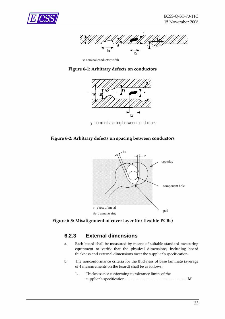
NOTE Intermittent and irregular metallisation defects on conductors are edge roughness (peak or valley), pits, pin holes, voids, protrusions or indentations, as shown in Figure 6‐1, Figure 6‐2 and Figure 6‐3.
22
ECSS‐Q‐ST‐70‐11C 15 November 2008
x: nominal conductor width
Figure 6‐1: Arbitrary defects on conductors
x
y: nominal spacing between conductors
Figure 6‐2: Arbitrary defects on spacing between conductors
r : rest of metal
δe : annular ring
coverlay
component hole
pad
δe r
Figure 6‐3: Misalignment of cover layer (for flexible PCBs)
6.2.3 External dimensions a. Each board shall be measured by means of suitable standard measuring
equipment to verify that the physical dimensions, including board thickness and external dimensions meet the supplier’s specification.
b. The nonconformance criteria for the thickness of base laminate (average of 4 measurements on the board) shall be as follows:
1. Thickness not conforming to tolerance limits of the supplier’s specification .................................................................M
23
ECSS‐Q‐ST‐70‐11C 15 November 2008
c. The nonconformance criteria for the length and width of board (average of 2 measurements on the board) shall be as follows:
1. Length or width not conforming to tolerance limits of the supplier’s specification .................................................................M
6.2.4 Warp a. The PCBs shall be placed unrestrained on a plane horizontal surface with
the convex side upward.
b. The warp shall be expressed in percentage terms.
c. The maximum bow between the plane horizontal surface and the PCB shall be measured as defined in Figure 6‐4.
d. The length of the PCB shall be measured.
e. The warp percentage shall be calculated as defined in equation [6‐1]:
100)(
)(.(%) ×=mmPCBtheofLength
mmblowMaxWarp [6‐1]
f. The nonconformance criteria shall be as follows:
1. Warp > requirement......................................................................M
max. bow
Figure 6‐4: Warp
6.2.5 Twist a. The PCB shall be placed on a plane horizontal surface so that it rests on
three corners.
b. The twist shall be expressed in percentage terms.
c. The distance between the plane horizontal surface and the fourth corner of the PCB shall be measured as defined in Figure 6‐5.
d. The length of the diagonal shall be measured.
e. The twist percentage shall be calculated as defined in equation [6‐2].
100)(
)(.(%) ×=mmdiagonaltheofLength
mmtwistMaxTwist [6‐2]
f. The nonconformance criteria shall be as follows:
1. Twist > requirement......................................................................M
24

ECSS‐Q‐ST‐70‐11C 15 November 2008
A, B and C are touching base
max. twist
Figure 6‐5: Twist
6.3 Microsection inspection criteria
6.3.1 General a. The test shall be carried out in conformance with tests 1c and 15b of
IEC 60326‐2‐am 1 (1992‐06).
b. For high frequency conductors the customer shall specify at which height of the conductor the width shall be measured (see Figure 6‐6).
w width of conductor δe minimum annular erring on external layer δe minimum annular erring on internal layer d diameter of plated‐through hole h height of conductor
Figure 6‐6: Dimensional parameters to be measured
25

ECSS‐Q‐ST‐70‐11C 15 November 2008
6.3.2 Thickness of metal-plating a. The test shall be carried out on a microsection.
b. Observations shall be made with magnification greater than or equal to ×250.
c. The nonconformance criteria for the thickness of copper plating on external layers shall be as follows:
1. Basic copper:
(a) Thickness not conforming to the supplier’s specification......................................................M
2. Basic copper plus electrolytic copper on non‐soldering areas:
(a) Thickness < requirement...................................................M
3. Basic copper plus electrolytic copper soldering pads (see Figure 6‐7 number 2):
(a) Thickness < 40 μm..............................................................M
d. The nonconformance criteria for the thickness of copper in plated‐through holes that are component holes shall be as follows:
1. Average thickness based on 3 measurements taken on the hole walls (see Figure 6‐7 number 1):
(a) Thickness < requirement...................................................M
e. The nonconformance criteria for the thickness of copper layer on internal layers shall be as follows:
1. Thickness not conforming to supplier’s specification..............M
f. The nonconformance criteria for the thickness of copper in plated‐through holes that are vias, buried vias or blind vias shall be as follows:
1. Thickness < requirement ..............................................................M
g. The nonconformance criteria for the thickness of tin‐lead alloy on surface, measured along the conductor longitudinal axis, shall be as follows:
1. 5 μm < thickness < 8 μm ...............................................................m
2. Thickness < 5 μm...........................................................................M
h. The nonconformance criteria for the thickness of tin‐lead alloy in holes shall be as follows:
1. In highest part of half of the hole wall height (see Figure 6‐7 number 3): thickness < 8 μm........................................................M
2. On angle of hole corner (see Figure 6‐7 number 4): 1 μm < thickness < 2 μm ...............................................................m
3. On angle of hole corner (see Figure 6‐7 number 4): thickness < 1 μm ............................................................................M
26

ECSS‐Q‐ST‐70‐11C 15 November 2008
Key 1 = Cu in PTH 2 = Cu at surface pattern 3 = SnPB in hole 4 = SnPb in angle area internal buging b < a
Figure 6‐7: Microsection of a PTH
i. The nonconformance criteria for the thickness of electrolytic Au or Au/Ni on surface and in holes (measured along the conductor longitudinal axis) shall be as follows:
1. Au for manual soldering on nickel:
(a) Thickness < 1 μm................................................................M
(b) Thickness > 7 μm................................................................M
2. Au for manual soldering on copper:
(a) Thickness < 3 μm................................................................M
(b) Thickness > 7 μm................................................................M
3. Au for high frequency circuits or other assembly methods ‐ as specified by customer:
(a) Thickness not conforming to tolerance limits of ........... supplier’s specification......................................................M
4. Ni:
(a) Thickness < 2 μm................................................................M
(b) Thickness > 10 μm..............................................................M
j. The nonconformance criteria for the distance between SnPb and Au overlap and the termination pad designated for soldering shall be as follows:
1. Distance < 200 μm .........................................................................M
k. The nonconformance criteria for the etch undercut on external and internal layers for fused SnPb (see Figure 6‐8) shall be as follows:
1. Undercut (u) > total copper thickness (h) ..................................M
27

ECSS‐Q‐ST‐70‐11C 15 November 2008
l. The nonconformance criteria for the etch undercut on external and internal layers for Au plating with or without Ni finish (see Figure 6‐9) shall be as follows:
1. If undercut (d) > 30 μm.................................................................M
m. The nonconformance criteria for the etch overhang on external layers for Au plating with or without Ni finish (see Figure 6‐10) shall be as follows:
1. If overhang (D) > 2× thickness of total copper ..........................M
NOTE For high frequency application overhang is normally undesirable and can be removed mechanically.
h
u
Cu elect.
Cu basic
SnPb
Figure 6‐8: Undercut for PCBs with fused SnPb finish
Au/NiAu/Ni
CuCu elect.
Cu basic
d dundercut undercut
Figure 6‐9: Undercut for PCBs with Au/Ni or Au finish
Au/Ni
Cu elect.
Cu basic
D Overhang
Figure 6‐10: Overhang for PCBs with Au/Ni or Au finish
6.3.3 Aspect of plated-through holes a. Sections of plated‐through holes shall be observed with magnification
greater than or equal to ×100.
28

ECSS‐Q‐ST‐70‐11C 15 November 2008
b. Layer misregistration compared to the minimum annular ring on pads.
c. The nonconformance criteria for the layer misregistration on the external layer (see Figure 6‐6) shall be as follows:
1. δe < requirement............................................................................M
d. The nonconformance criteria for the layer misregistration on the internal layers (see Figure 6‐6) shall be as follows:
1. δi < requirement.............................................................................M
2. Minimum insulation between layers < requirement................M
e. The nonconformance criteria for irregular drilling (see Figure 6‐11) shall be as follows:
1. Infiltration of metal into base laminate:
(a) 40 μm < infiltration < 80 μm..............................................m
(b) Infiltration> 80 μm .............................................................M
2. Presence of adhesive on basic copper not leading to rupture during fusing process or thermal shock ......................m
3. Adhesion defects between metal‐plating and basic copper ....M
4. Adhesion defects between metal‐plating and inner layers .....M
5. Resin smear on the interface between internal conductor and plated copper greater than 15 % of conductor thickness .M
6. Void in resin greater than 50 % of basic copper thickness.......M
Figure 6‐11: Microsection in PTH: Possible defects
f. The nonconformance criteria for voids in PCB base laminate substrate and resin recession in holes (see Figure 6‐12) shall be as follows:
1. Voids in the PCB base laminate substrate:
(a) Lc > 80 μm...........................................................................M
29

ECSS‐Q‐ST‐70‐11C 15 November 2008
2. At edge of metal‐plating:
(a) Sum of resin recession hc > 20 % sum hi..........................M
3. Resin recession in hole before or after test:
(a) Resin recession between 10 % and 20 % of height of hole ..................................................................................m
(b) If resin recession > 20 % of height of hole.......................M
g. The nonconformance criteria for the copper plating inside buried, blind, via and component holes shall be as follows:
1. Void in copper plating in holes ...................................................M
h. The nonconformance criteria for the resin inside buried vias shall be in conformance with Figure 6‐13.
hi = insulation distance
hc = height of resin recession
Lc = size of the void
hi hc
Lc
Laminate void
Resin recession
Figure 6‐12: Microsection of PTH: Possible defects
not acceptable acceptable
Figure 6‐13: Voids in resin inside buried vias
30

ECSS‐Q‐ST‐70‐11C 15 November 2008
7 Requirements for PCBs
7.1 Rigid single-sided and double-sided PCBs a. The base materials shall be in conformance with ECSS‐Q‐ST‐70, IEC
specifications and IPC‐4101 and shall be one of the following:
1. Woven‐glass‐reinforced epoxy resin FR4;
2. Woven‐glass‐reinforced polyimide resin.
b. The limits for the dimensional characteristics shall be as follows:
1. External dimension tolerance: ±0,2 mm;
2. Thickness tolerance: ±10 %;
3. Active board size, maximum: supplier’s specification;
4. Board thickness maximum: 3,2 mm;
5. Positioning tolerance between registration mark and edge of circuit: ±0,2 mm;
6. Conductor width: 200 μm minimum (for fine pitch 120 μm width is tolerated if less than 5 mm from component pad);
7. Spacing between conductors: 300 μm minimum (for fine pitch 150 μm spacing is tolerated if less than 5 mm from component pad);
8. Conductor tolerance (minimum/maximum): supplier’s specification, ±20 % maximum;
9. Tolerance on diameter of terminal pads: supplier’s specification, ±20 % maximum;
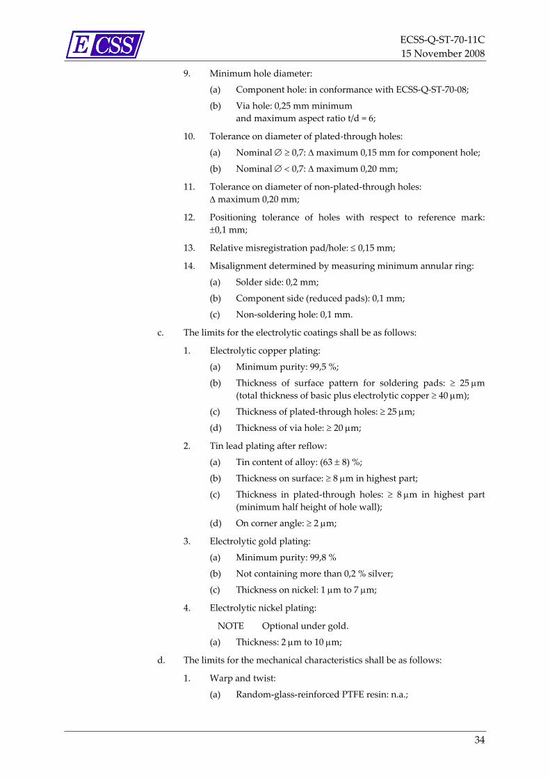
10. Minimum hole diameter:
(a) Component hole: in conformance with ECSS‐Q‐ST‐70‐08;
(b) Via hole: 0,25 mm minimum and maximum aspect ratio t/d = 6;
11. Tolerance on diameter of plated‐through holes:
(a) Nominal ∅ ≥ 0,7 mm: Δ maximum 0,15 mm for component hole;
(b) Nominal ∅ < 0,7 mm: Δ maximum 0,20 mm;
12. Tolerance on diameter of non‐plated‐through holes: Δ maximum 0,20 mm;
31

ECSS‐Q‐ST‐70‐11C 15 November 2008
13. Positioning tolerance of holes with respect to reference mark: ±0,1 mm;
14. Relative misregistration pad/hole: ≤ 0,15 mm;
15. Misalignment determined by measuring minimum annular ring:
(a) Solder side: 0,20 mm;
(b) Component side (reduced pads): 0,10 mm;
(c) Non‐soldering hole: 0,10 mm.
c. The limits for the electrolytic coatings are as follows:
1. Electrolytic copper plating:
(a) Minimum purity: 99,5 %;
(b) Thickness of surface pattern: ≥ 25 μm;
(c) Thickness of plated‐through holes: ≥ 25 μm;
(d) Thickness of via holes: ≥ 20 μm;
2. Tin lead plating after reflow:
(a) Tin content of alloy: (63 ± 8) %;
(b) Thickness on surface: 8 μm in highest part;
(c) Thickness in plated‐through holes: 8 μm in highest part (minimum half height of hole wall);
(d) Thickness on corner angle: 2 μm;
3. Electrolytic gold plating:
(a) Minimum purity: 99,8 % (not more than 0,2 % silver);
(b) Thickness on nickel: (4 ± 3) μm;
(c) Thickness on copper: (5 ± 2) μm;
4. Electrolytic nickel plating:
(a) Thickness: 2 μm to 10 μm.
NOTE Electrolytic nickel plating is optional under gold.
d. The limits for the mechanical characteristics are as follows:
1. Warp and twist: ≤ 1,1 % for board thickness ≥ 1,6 mm, ≤ 1,5 % for board thickness < 1,6 mm;
2. Conductor adhesion/peel strength:
(a) On epoxy: ≥ 16 N/cm;
(b) On polyimide: ≥ 12 N/cm;
3. Pull strength:
(a) For terminal pads 4 mm ∅ on epoxy: ≥ 140 N;
(b) For terminal pads 4 mm ∅ on polyimide: ≥ 80 N;
(c) For terminal pads 2 mm ∅ on epoxy: ≥ 35 N;
(d) For terminal pads 2 mm ∅ on polyimide: ≥ 20 N.
32

ECSS‐Q‐ST‐70‐11C 15 November 2008
e. The limits for the electrical characteristics are as follows:
1. Insulation resistance:
(a) Intralayer (i.e. in the same layer): > 104 MΩ;
(b) Interlayer (i.e. between opposite layers): > 105 MΩ;
2. Withstanding voltage per mm spacing between conductors:
(a) Intralayer and interlayer: 1 000 V r.m.s;
3. Short time overload:
(a) 0,035 mm copper thickness: 7 A for 4 s;
(b) 0,070 mm copper thickness: 14 A for 4 s;
4. Long time overload, destructive current:
(a) 0,035 mm copper thickness: I ≥ 8 A;
(b) 0,070 mm copper thickness: I ≥ 16 A.
7.2 Rigid single-sided and double-sided PCBs for high frequency application
a. The base materials shall be in conformance with ECSS‐Q‐ST‐70, IEC specifications and IPC‐4101 and shall be on of the following:
1. Random‐glass‐reinforced PTFE resin with or without Al backing;
2. Woven‐glass‐reinforced PTFE resin;
3. Ceramic filled woven‐glass‐reinforced PTFE resin;
4. Ceramic filled PTFE resin with or without Al backing;
5. Ceramic filled cross‐linked hydrocarbon/thermoset polymer;
6. Woven‐glass‐reinforced epoxy resin FR4;
7. Quartz filled polyimide resin.
b. The limits for the dimensional characteristics shall be as follows:
1. External dimension tolerance: ±0,2 mm;
2. Thickness tolerance: ±10 %;
3. Active board size, maximum: supplier’s specification;
4. Board thickness (minimum/maximum): customer’s and supplier’s specification according to electrical performance;
5. Positioning tolerance between registration mark and edge of circuit: ±0,2 mm;
6. Conductor width/spacing: customer’s and supplier’s specification according to electrical performance;
7. Tolerance on conductor (minimum/maximum): supplier’s specification;
8. Tolerance on diameter of terminal pads: customer’s and supplier’s specification according to electrical performance;
33
ECSS‐Q‐ST‐70‐11C 15 November 2008
9. Minimum hole diameter:
(a) Component hole: in conformance with ECSS‐Q‐ST‐70‐08;
(b) Via hole: 0,25 mm minimum and maximum aspect ratio t/d = 6;
10. Tolerance on diameter of plated‐through holes:
(a) Nominal ∅ ≥ 0,7: Δ maximum 0,15 mm for component hole;
(b) Nominal ∅ < 0,7: Δ maximum 0,20 mm;
11. Tolerance on diameter of non‐plated‐through holes: Δ maximum 0,20 mm;
12. Positioning tolerance of holes with respect to reference mark: ±0,1 mm;
13. Relative misregistration pad/hole: ≤ 0,15 mm;
14. Misalignment determined by measuring minimum annular ring:
(a) Solder side: 0,2 mm;
(b) Component side (reduced pads): 0,1 mm;
(c) Non‐soldering hole: 0,1 mm.
c. The limits for the electrolytic coatings shall be as follows:
1. Electrolytic copper plating:
(a) Minimum purity: 99,5 %;
(b) Thickness of surface pattern for soldering pads: ≥ 25 μm (total thickness of basic plus electrolytic copper ≥ 40 μm);
(c) Thickness of plated‐through holes: ≥ 25 μm;
(d) Thickness of via hole: ≥ 20 μm;
2. Tin lead plating after reflow:
(a) Tin content of alloy: (63 ± 8) %;
(b) Thickness on surface: ≥ 8 μm in highest part;
(c) Thickness in plated‐through holes: ≥ 8 μm in highest part (minimum half height of hole wall);
(d) On corner angle: ≥ 2 μm;
3. Electrolytic gold plating:
(a) Minimum purity: 99,8 %
(b) Not containing more than 0,2 % silver;
(c) Thickness on nickel: 1 μm to 7 μm;
4. Electrolytic nickel plating:
NOTE Optional under gold.
(a) Thickness: 2 μm to 10 μm;
d. The limits for the mechanical characteristics shall be as follows:
1. Warp and twist:
(a) Random‐glass‐reinforced PTFE resin: n.a.;
34
ECSS‐Q‐ST‐70‐11C 15 November 2008
(b) Woven‐glass‐reinforced PTFE resin: n.a.;
(c) Ceramic filled PTFE resin: ≤ 1,1 %;
(d) Ceramic filled x‐linked hydrocarbon/thermoset polymer: ≤ 1,1 %;
(e) Woven‐glass‐reinforced epoxy resin FR4: ≤ 1,1 % for board thickness ≥ 1,6 mm, ≤ 1,5 % for board thickness < 1,6 mm;
(f) Quartz filled polyimide: ≤ 1,1 % for board thickness ≥ 1,6 mm, ≤ 1,5 % for board thickness < 1,6 mm;
2. Conductor adhesion/peel strength:
(a) On PTFE reinforced/ceramic filled or non‐filled: ≥ 8 N/cm;
(b) Cross‐linked hydrocarbon: ≥ 8 N/cm;
(c) On epoxy: ≥ 16 N/cm;
(d) On polyimide quartz: ≥ 12 N/cm;
3. Pull strength:
(a) For terminal pads 4 mm ∅ on PTFE reinforced/ceramic filled or non‐filled: ≥ 60 N;
(b) For terminal pads 4 mm ∅ cross‐linked hydrocarbon: ≥ 60 N;
(c) For terminal pads 4 mm ∅ on epoxy: ≥ 140 N;
(d) For terminal pads 4 mm ∅ on polyimide quartz: ≥ 60 N;
(e) For terminal pads 2 mm ∅ on PTFE reinforced /ceramic filled or non‐filled: ≥ 12 N;
(f) For terminal pads 2 mm ∅ cross‐linked hydrocarbon: ≥ 12 N;
(g) For terminal pads 2 mm ∅ on epoxy: ≥ 35 N;
(h) For terminal pads 2 mm ∅ on polyimide quartz: ≥ 20 N.
e. The limits for the electrical characteristics shall be as follows:
1. Insulation resistance:
(a) Intralayer: > 104 MΩ;
(b) Interlayer: > 105 MΩ;
2. Withstanding voltage per mm spacing between conductors:
(a) Intralayer and interlayer: 1 000 V r.m.s.;
3. Short time overload:
(a) 0,009 mm copper thickness: n.a.;
(b) 0,017 mm copper thickness: n.a.;
(c) 0,035 mm copper thickness: 7 A for 4 s;
(d) 0,070 mm copper thickness: 14 A for 4 s;
4. Long time overload, destructive current:
(a) 0,009 mm copper thickness: n.a.;
35
ECSS‐Q‐ST‐70‐11C 15 November 2008
(b) 0,017 mm copper thickness: n.a.;
(c) 0,035 mm copper thickness: I ≥ 8 A;
(d) 0,070 mm copper thickness: I ≥ 16 A;
5. Permittivity: customer’s and supplier’s specification according to electrical performance;
6. Loss angle Tg δ: customer’s and supplier’s specification according to electrical performance.
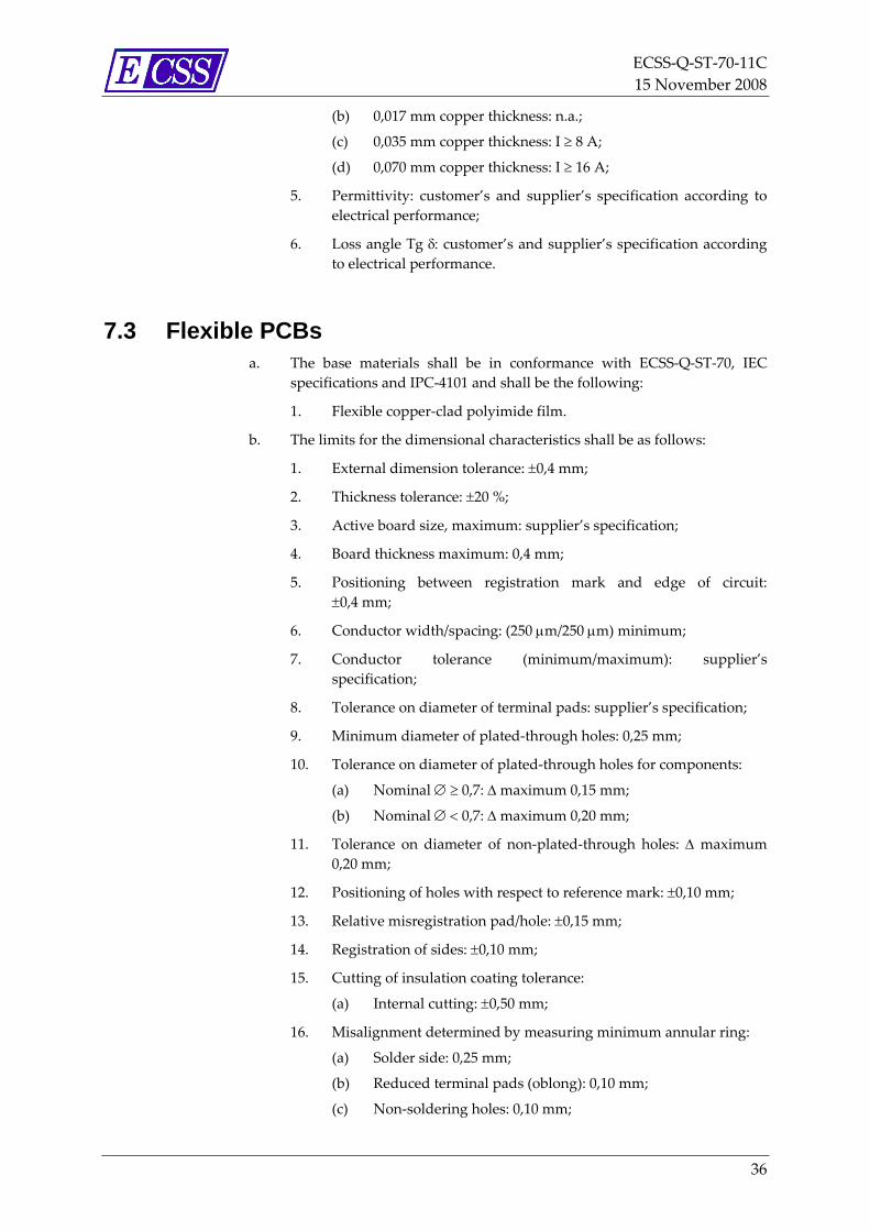
7.3 Flexible PCBs a. The base materials shall be in conformance with ECSS‐Q‐ST‐70, IEC
specifications and IPC‐4101 and shall be the following:
1. Flexible copper‐clad polyimide film.
b. The limits for the dimensional characteristics shall be as follows:
1. External dimension tolerance: ±0,4 mm;
2. Thickness tolerance: ±20 %;
3. Active board size, maximum: supplier’s specification;
4. Board thickness maximum: 0,4 mm;
5. Positioning between registration mark and edge of circuit: ±0,4 mm;
6. Conductor width/spacing: (250 μm/250 μm) minimum;
7. Conductor tolerance (minimum/maximum): supplier’s specification;
8. Tolerance on diameter of terminal pads: supplier’s specification;
9. Minimum diameter of plated‐through holes: 0,25 mm;
10. Tolerance on diameter of plated‐through holes for components:
(a) Nominal ∅ ≥ 0,7: Δ maximum 0,15 mm;
(b) Nominal ∅ < 0,7: Δ maximum 0,20 mm;
11. Tolerance on diameter of non‐plated‐through holes: Δ maximum 0,20 mm;
12. Positioning of holes with respect to reference mark: ±0,10 mm;
13. Relative misregistration pad/hole: ±0,15 mm;
14. Registration of sides: ±0,10 mm;
15. Cutting of insulation coating tolerance:
(a) Internal cutting: ±0,50 mm;
16. Misalignment determined by measuring minimum annular ring:
(a) Solder side: 0,25 mm;
(b) Reduced terminal pads (oblong): 0,10 mm;
(c) Non‐soldering holes: 0,10 mm;
36

ECSS‐Q‐ST‐70‐11C 15 November 2008
17. Misalignment of insulation coating determined by measuring rest of metal:
(a) Plated‐through holes: 0,15 mm;
(b) Non‐plated‐through holes: 0,25 mm;
18. Number of layers: 2.
c. The limits for the electrolytic coatings shall be as follows:
1. Electrolytic copper plating:
(a) Minimum purity: 99,5 %;
(b) Thickness of surface pattern: ≥ 25 μm;
(c) Thickness of plated‐through holes: ≥ 25 μm;
2. Tin lead plating after reflow:
(a) Tin content of alloy: (63 ± 8) %;
(b) Thickness on surface: ≥ 8 μm in highest part;
(c) Thickness in plated‐through holes: ≥ 8 μm in highest part (minimum half height of hole wall);
(d) On corner angle: ≥ 2 μm.
d. The limits for the mechanical characteristics shall be as follows:
1. Conductor adhesion/peel strength: ≥ 10 N/cm;
2. Pull strength:
(a) For terminal pads 4 mm ∅: ≥ 60 N;
(b) For terminal pads 2 mm ∅: ≥ 12 N;
3. Resistance to bending cycles: ≥ 250 cycles;
4. Bending test for rigid‐flex boards: ≥ 25 cycles.
e. The limits for the electrical characteristics shall be as follows:
1. Insulation resistance:
(a) Intralayer: ≥ 104 MΩ;
(b) Interlayer: ≥ 105 MΩ;
(c) With temperature at 80 °C: ≥ 102 MΩ;
2. Withstanding voltage per mm spacing between conductors: 1 000 V r.m.s.;
3. Short time overload: 7 A for 4 s;
4. Long time overload, destructive current: ≥ 8 A.
7.4 Rigid-flex PCBs a. The requirements for rigid‐flex PCBs shall be in conformance with clause
7.3 for the flexible part and clause 7.5 for the rigid part.
b. For the construction of multilayer rigid‐flex the flexible copper clad polyimide film shall be without adhesive
37
ECSS‐Q‐ST‐70‐11C 15 November 2008
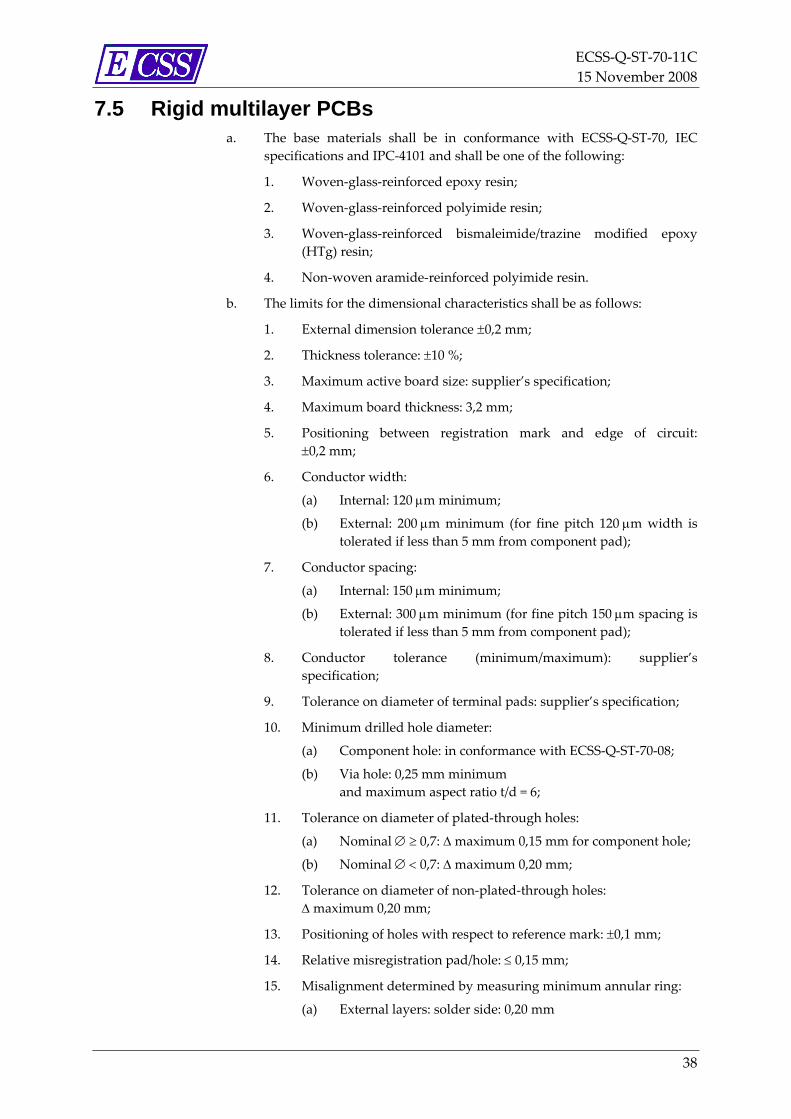
7.5 Rigid multilayer PCBs a. The base materials shall be in conformance with ECSS‐Q‐ST‐70, IEC
specifications and IPC‐4101 and shall be one of the following:
1. Woven‐glass‐reinforced epoxy resin;
2. Woven‐glass‐reinforced polyimide resin;
3. Woven‐glass‐reinforced bismaleimide/trazine modified epoxy (HTg) resin;
4. Non‐woven aramide‐reinforced polyimide resin.
b. The limits for the dimensional characteristics shall be as follows:
1. External dimension tolerance ±0,2 mm;
2. Thickness tolerance: ±10 %;
3. Maximum active board size: supplier’s specification;
4. Maximum board thickness: 3,2 mm;
5. Positioning between registration mark and edge of circuit: ±0,2 mm;
6. Conductor width:
(a) Internal: 120 μm minimum;
(b) External: 200 μm minimum (for fine pitch 120 μm width is tolerated if less than 5 mm from component pad);
7. Conductor spacing:
(a) Internal: 150 μm minimum;
(b) External: 300 μm minimum (for fine pitch 150 μm spacing is tolerated if less than 5 mm from component pad);
8. Conductor tolerance (minimum/maximum): supplier’s specification;
9. Tolerance on diameter of terminal pads: supplier’s specification;
10. Minimum drilled hole diameter:
(a) Component hole: in conformance with ECSS‐Q‐ST‐70‐08;
(b) Via hole: 0,25 mm minimum and maximum aspect ratio t/d = 6;
11. Tolerance on diameter of plated‐through holes:
(a) Nominal ∅ ≥ 0,7: Δ maximum 0,15 mm for component hole;
(b) Nominal ∅ < 0,7: Δ maximum 0,20 mm;
12. Tolerance on diameter of non‐plated‐through holes: Δ maximum 0,20 mm;
13. Positioning of holes with respect to reference mark: ±0,1 mm;
14. Relative misregistration pad/hole: ≤ 0,15 mm;
15. Misalignment determined by measuring minimum annular ring:
(a) External layers: solder side: 0,20 mm
38
ECSS‐Q‐ST‐70‐11C 15 November 2008
(b) External layers: component side (reduced pads): 0,10 mm
(c) External layers: non‐soldering hole: 0,10 mm
(d) Internal layers: 50 μm;
16. Layer to layer registration: ±100 μm;
17. Number of layers: 18 maximum.
c. The limits for the electrolytic coatings shall be as follows:
1. Electrolytic copper plating:
(a) Minimum purity: 99,5 %;
(b) Thickness of surface pattern: ≥ 25 μm;
(c) Thickness of plated‐through holes: ≥ 25 μm;
(d) Thickness of via holes: ≥ 20 μm;
2. Tin lead plating after reflow:
(a) Tin content of alloy: (63 ± 8) %;
(b) Thickness on surface: ≥ 8 μm in highest part;
(c) Thickness in plated‐through holes: ≥ 8 μm in highest part (minimum half height of hole wall);
(d) On corner angle: ≥ 2 μm;
3. Electrolytic gold plating:
(a) Minimum purity: 99,8 %
(b) Not containing more than 0,2 % silver;
(c) Thickness on nickel: (4 ± 3) μm;
(d) Thickness on copper: (5 ± 2) μm;
4. Electrolytic nickel plating:
NOTE Optional under gold.
(a) Thickness: 2 μm to 10 μm;
5. Insulation between layers: 70 μm minimum.
d. The limits for the mechanical characteristics shall be as follows:
1. Warp and twist: ≤ 1,1 % for board thickness ≥ 1,6 mm, ≤ 1,5 % for board thickness < 1,6 mm;
2. Conductor adhesion/peel strength:
(a) On epoxy with Tg < 160 °C: ≥ 16 N/cm;
(b) On epoxy with Tg > 180 °C: ≥ 12 N/cm;
(c) On polyimide: ≥ 12 N/cm;
(d) On bismaleimide/trazine modified epoxy HTg: ≥ 12 N/cm;
(e) Aramide/polyimide: ≥ 6 N/cm;
3. Bond strength/pull strength:
(a) For terminal pads 4 mm ∅ on epoxy Tg < 160 °C: ≥ 140 N;
(b) For terminal pads 4 mm ∅ on epoxy Tg > 180 °C: ≥ 80 N;
39
ECSS‐Q‐ST‐70‐11C 15 November 2008
(c) For terminal pads 4 mm ∅ on polyimide: ≥ 80 N;
(d) For terminal pads 4 mm ∅ on bismaleimide/trazine modified epoxy HTg: ≥ 60 N;
(e) For terminal pads 4 mm ∅ on aramide/polyimide: ≥ 60 N;
(f) For terminal pads 2 mm ∅ on epoxy Tg < 160 °C: ≥ 35 N;
(g) For terminal pads 2 mm ∅ on epoxy Tg > 180 °C: ≥ 20 N;
(h) For terminal pads 2 mm ∅ on polyimide: ≥ 20 N;
(i) For terminal pads 2 mm ∅ on bismaleimide/trazine modified epoxy HTg: ≥ 12 N;
(j) For terminal pads 2 mm ∅ on aramide/polyimide: ≥ 12 N.
e. The limits for the electrical characteristics shall be as follows:
1. Insulation resistance:
(a) Intralayer: > 104 MΩ;
(b) Interlayer: > 105 MΩ;
2. Withstanding voltage per mm spacing between conductors:
(a) Intralayer and interlayer: 1 000 V r.m.s.;
3. Short time overload:
(a) 35 μm copper thickness: 7 A for 4 s;
(b) 70 μm copper thickness: 14 A for 4 s;
4. Long time overload, destructive current:
(a) 35 μm copper thickness: I ≥ 8 A;
(b) 70 μm copper thickness: I ≥ 16 A;
5. Internal short circuit:
(a) Insulation resistance: ≥ 103 MΩ.
7.6 Sequential rigid multilayer PCBs a. The base materials shall be in conformance with ECSS‐Q‐ST‐70, IEC
specifications and IPC‐4101 and shall be one of the following:
1. Woven‐glass‐reinforced epoxy resin;
2. Woven‐glass‐reinforced polyimide resin;
3. Woven‐glass‐reinforced bismaleimide/trazine modified epoxy (HTg) resin;
4. Non‐woven‐aramide‐reinforced polyimide resin.
b. The limits for the dimensional characteristics shall be as follows:
1. External dimension tolerance: ±0,2 mm;
2. Thickness tolerance: ±10 %;
3. Maximum active board size: supplier’s specification;
4. Maximum board thickness: 3,2 mm;
40

ECSS‐Q‐ST‐70‐11C 15 November 2008
5. Positioning between registration mark and edge of circuit: Δ maximum 0,20 mm;
6. Conductor width:
(a) Internal: 120 μm minimum;
(b) External: 200 μm minimum (for fine pitch 120 μm width is tolerated if less than 5 mm from component pad);
7. Conductor spacing:
(a) Internal: 150 μm minimum;
(b) External: 300 μm minimum (for fine pitch 150 μm spacing is tolerated if less than 5 mm from component pad);
8. Conductor tolerance (minimum/maximum): supplier’s specification;
9. Tolerance on diameter of terminal pads: supplier’s specification;
10. Minimum drilled hole diameter:
(a) Component hole: in conformance with ECSS‐Q‐ST‐70‐08;
(b) Via hole: 0,25 mm minimum and maximum aspect ratio t/d = 6;
(c) Buried via: supplier’s specification and maximum aspect ratio t/d = 6;
(d) Blind via produced sequentially: supplier’s specification and maximum aspect ratio t/d = 6;
11. Tolerance on diameter of plated‐through holes:
(a) Nominal ∅ ≥ 0,7: Δ maximum 0,15 mm for component hole;
(b) Nominal ∅ < 0,7: Δ maximum 0,20 mm;
12. Tolerance on diameter of non‐plated‐through holes: Δ maximum 0,20 mm;
13. Positioning of holes with respect to reference mark: ±0,10 mm;
14. Relative misregistration pad/hole: ≤ 0,15 mm;
15. Misalignment determined by measuring minimum annular ring:
(a) External layers: solder side: 0,20 mm;
(b) External layers: component side (reduced pads): 0,10 mm;
(c) External layers: non‐soldering hole: 0,10 mm;
(d) Internal layers: 0,05 mm;
16. Layer to layer registration: ±100 μm;
17. Number of layers: 18 maximum.
c. The limits for the electrolytic coatings shall be as follows:
1. Electrolytic copper plating:
(a) Minimum purity: 99,5 %;
(b) Thickness of surface pattern: ≥ 25 μm;
(c) Thickness of plated‐through holes: ≥ 25 μm;
41

ECSS‐Q‐ST‐70‐11C 15 November 2008
(d) Thickness of via holes: ≥ 20 μm;
(e) Thickness of buried via holes: ≥ 18 μm;
(f) Thickness of blind via holes: ≥ 18 μm;
2. Tin lead plating after reflow:
(a) Tin content of alloy: (63 ± 8) %;
(b) Thickness on surface: ≥ 8 μm in highest part;
(c) Thickness in plated‐through holes: ≥ 8 μm highest part (minimum half height of hole wall);
(d) On corner angle: ≥ 2 μm;
3. Electrolytic gold plating:
(a) Minimum purity: 99,8 %
(b) Not containing more than 0,2 % silver;
(c) Thickness on nickel: (4 ± 3) μm;
(d) Thickness on copper: (5 ± 2) μm;
4. Electrolytic nickel plating:
(a) Thickness: 2 μm to 10 μm;
NOTE Electrolytic nickel plating is optional under gold.
5. Resin fill in buried vias: see 6.3.3h;
6. Insulation between layers: 70 μm minimum.
d. The limits for the mechanical characteristics shall be as follows:
1. Warp and twist: ≤ 1,1 % for board thickness ≥ 1,6 mm, ≤ 1,5 % for board thickness < 1,6 mm;
2. Conductor adhesion/peel strength:
(a) On epoxy with Tg < 160 °C: ≥ 16 N/cm;
(b) On epoxy with Tg > 180 °C: ≥ 12 N/cm;
(c) On polyimide: ≥ 12 N/cm;
(d) On bismaleimide/trazine modified epoxy HTg: ≥ 12 N/cm;
(e) Aramide/polyimide: ≥ 6 N/cm;
3. Bond strength/pull strength:
(a) For terminal pads 4 mm ∅ on epoxy Tg < 160 °C: ≥ 140 N;
(b) For terminal pads 4 mm ∅ on epoxy Tg > 180 °C: ≥ 80 N;
(c) For terminal pads 4 mm ∅ on polyimide: ≥ 80 N;
(d) For terminal pads 4 mm ∅ on bismaleimide/trazine modified epoxy HTg: ≥ 60 N;
(e) For terminal pads 4 mm ∅ on aramide/polyimide: ≥ 60 N;
(f) For terminal pads 2 mm ∅ on epoxy Tg < 160 °C: ≥ 35 N;
(g) For terminal pads 2 mm ∅ on epoxy Tg > 180 °C: ≥ 20 N;
(h) For terminal pads 2 mm ∅ on polyimide: ≥ 20 N;
42
ECSS‐Q‐ST‐70‐11C 15 November 2008
(i) For terminal pads 2 mm ∅ on bismaleimide/trazine modified epoxy HTg: ≥ 12 N;
(j) For terminal pads 2 mm ∅ aramide/polyimide: ≥ 12 N.
e. The limits for the electrical characteristics shall be as follows:
1. Insulation resistance:
(a) Intralayer: > 104 MΩ;
(b) Interlayer: > 105 MΩ;
2. Withstanding voltage per mm spacing between conductors:
(a) Intralayer and interlayer: 1 000 V r.m.s.;
3. Short time overload:
(a) 0,035 mm copper thickness: 7 A for 4 s;
(b) 0,070 mm copper thickness: 14 A for 4 s;
4. Long time overload, destructive current:
(a) 0,035 mm copper thickness: I ≥ 8 A;
(b) 0,070 mm copper thickness: I ≥ 16 A;
5. Internal short circuit:
(a) Insulation resistance: ≥ 103 MΩ.
43
ECSS‐Q‐ST‐70‐11C 15 November 2008
Annex A (normative) PCB Certificate of conformance (CoC) –
DRD
A.1 DRD identification
A.1.1 Requirement identification and source document This DRD is called from ECSS‐Q‐ST‐70‐11, requirements 5.3.3d.1 and 5.4.2k.
A.1.2 Purpose and objective The purpose of the DRD is to describe the content of the PCB Certificate of conformance (CoC) document.
A.2 Expected response
A.2.1 Scope and content
<1> Contents a. The PCB CoC shall contain the following items:
1. List of base materials used;
2. Results of tests and inspections;
3. Associated test coupon (one per panel);
4. Microsection of as received plated‐through holes (one per panel);
5. Any approved nonconformance with the above specifications.
A.2.2 Special remarks a. The example PCB CoC document in Figure A‐1 may be used.
44
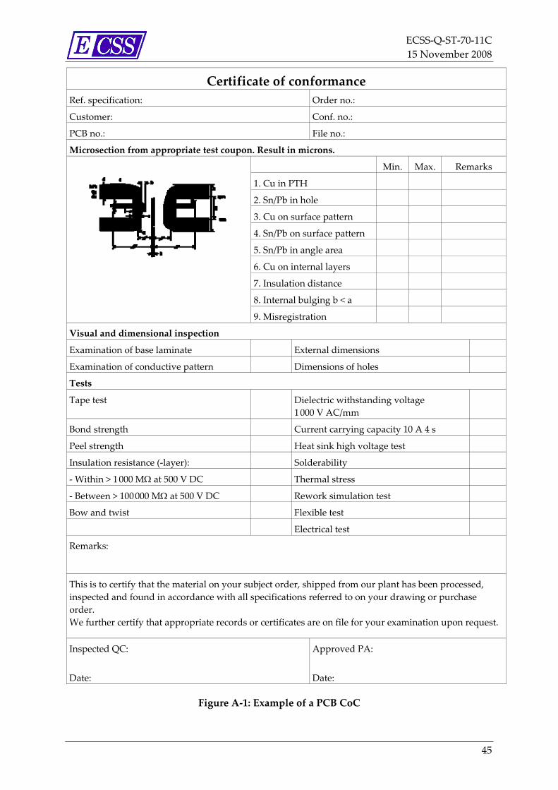
ECSS‐Q‐ST‐70‐11C 15 November 2008
Certificate of conformance Ref. specification: Order no.:
Customer: Conf. no.:
PCB no.: File no.:
Microsection from appropriate test coupon. Result in microns.
Min. Max. Remarks
1. Cu in PTH
2. Sn/Pb in hole
3. Cu on surface pattern
4. Sn/Pb on surface pattern
5. Sn/Pb in angle area
6. Cu on internal layers
7. Insulation distance
8. Internal bulging b < a
9. Misregistration
Visual and dimensional inspection
Examination of base laminate External dimensions
Examination of conductive pattern Dimensions of holes
Tests
Tape test Dielectric withstanding voltage 1 000 V AC/mm
Bond strength Current carrying capacity 10 A 4 s
Peel strength Heat sink high voltage test
Insulation resistance (‐layer): Solderability
‐ Within > 1 000 MΩ at 500 V DC Thermal stress
‐ Between > 100 000 MΩ at 500 V DC Rework simulation test
Bow and twist Flexible test
Electrical test
Remarks:
This is to certify that the material on your subject order, shipped from our plant has been processed, inspected and found in accordance with all specifications referred to on your drawing or purchase order. We further certify that appropriate records or certificates are on file for your examination upon request.
Inspected QC:
Date:
Approved PA:
Date:
Figure A‐1: Example of a PCB CoC
45

ECSS‐Q‐ST‐70‐11C 15 November 2008
Bibliography
ECSS‐S‐ST‐00 ECSS system – Description, implementation and general requirements
IEC 60194 (1999‐04) Printed board design, manufacture and assembly — Terms and definitions
46