source-synchronous timing with timequest€¦ · source-synchronous timing with timequest . wiki...
TRANSCRIPT

1
Source-Synchronous Timing with TimeQuest
Wiki Release 1.2 October 6th, 2011 By: Ryan Scoville Introduction: Although Altera has created much literature on source synchronous interfaces, I find it to still be one of the most difficult things to do in TimeQuest, and field questions quite often. There are many reasons for this difficulty. Third party datasheets spec their interfaces in many different ways. Altera’s literature provides multiple strategies for adding constraints, which allows flexibility but often leave users confused. Most material concentrates on entering constraints but without showing how to analyze the results. And perhaps most importantly, with multiple registers working off of multiple edges, the analysis is actually quite complex. This document is not meant to be a cook-book where the user just cuts and pastes the .sdc into their system. Instead, it starts with the most common and easy to understand scenarios and tries to explain how the constraints and analysis are done. The purpose is to help the user understand what each constraint does and how it relates to their system, so not only can they enter the correct constraint, they can feel confident that the analysis is correct. Once that framework has been built and hopefully understood, we will delve into corner cases and other scenarios that might cause confusion. Notes:
- This document is not mean for dedicated High-Speed SERDES(altlvds) built into many families. The following section discusses why.
- This document assumes the user is familiar with the TimeQuest User Guide at: http://www.alterawiki.com/wiki/TimeQuest_User_Guide Specifically Sections 1) Getting Started and 2) Timing Analysis Basics.
- I recommend turning on the Bookmarks when viewing this .pdf, allowing for easier navigation and to help understand the organization
Contact: TimeQuest support is not my primary responsibility, and so I will not be able to directly assist users. That being said, if there is anything ambiguous, incorrect, or missing, please contact me via www.alteraforum.com, sending an email to user Rysc. Be sure your account can accept emails too. I also monitor the forum a good amount and will try to answer questions there, as I much prefer helping with issues on the forum rather than direct email, since it can hopefully help multiple users. If you post something and I don’t respond, feel free to send me an email through the forum. That being said, if I am unable to respond, please don’t be offended. © 2011 Altera Corporation. The material in this wiki page or document is provided AS-IS and is not supported by Altera Corporation. Use the material in this document at your own risk; it might be, for example, objectionable, misleading or inaccurate.

2
Table of Contents
SECTION I: GETTING STARTED .......................................................................................................................... 4
ORGANIZATION – SUGGESTIONS FOR USING THIS DOCUMENT................................................................................... 4 SOURCE-SYNCHRONOUS BASICS ............................................................................................................................... 5 THE KEY TO SOURCE-SYNCHRONOUS PERFORMANCE ............................................................................................... 6 I/O TIMING BASICS .................................................................................................................................................... 7 INTRO TO TWO METHODS: EXPLICIT AND IMPLICIT CLOCK SHIFT ........................................................................... 10
SECTION II: THE EXPLICIT CLOCK SHIFT METHOD ................................................................................. 11 Case 1: The FPGA is the receiver and phase-shifts the clock ............................................................................ 13 Case 2: The FPGA is the receiver and does not phase-shift the clock ............................................................... 13 Case 3: FPGA is the transmitter and phase-shifts its clock ............................................................................... 16 Case 4: FPGA is the transmitter and sends a non-shifted clock ........................................................................ 17
EXTERNAL DELAYS OF THE EXPLICIT METHOD ....................................................................................................... 18 FPGA-Centric versus System-Centric ................................................................................................................ 20 Case 1 and Case 2: FPGA is the Receiver ......................................................................................................... 21 Case 3 and Case 4: FPGA is the Transmitter .................................................................................................... 22
BENEFITS OF THE EXPLICIT METHOD ....................................................................................................................... 24 REPORT_TIMING: PUTTING IT ALL TOGETHER .......................................................................................................... 24
SECTION III: THE IMPLICIT CLOCK SHIFT METHOD ............................................................................... 30
THE IMPLIED PHASE-SHIFT ...................................................................................................................................... 32 Case 5 : FPGA is Receiver, Implicit Method ..................................................................................................... 33 Case 6 : FPGA is Transmitter, Implicit Method ................................................................................................ 35
REALLY, THE INTERFACE HAS NO CLOCK SHIFT ..................................................................................................... 37
SECTION IV: SDR – SINGLE DATA RATE ........................................................................................................ 38
THE SDR EXPLICIT METHOD ................................................................................................................................... 39 Case 1: The FPGA is the receiver and centers the clock ................................................................................... 39 Case 2: The FPGA is the receiver and does not center the clock ...................................................................... 40 Case 3: FPGA is the transmitter and phase-shifts its clock ............................................................................... 40 Case 4: FPGA is the transmitter and sends a non-shifted clock ........................................................................ 41
THE SDR IMPLICIT METHOD ................................................................................................................................... 41 Case 5 : FPGA is Receiver, Implicit Method ..................................................................................................... 42 Case 6 : FPGA is Transmitter, Implicit Method ................................................................................................ 42
SECTION V: MISCELLANEOUS TOPICS .......................................................................................................... 42
EDGE-ALIGNED VERSUS CENTER-ALIGNED ............................................................................................................. 42 OUTPUT CLOCK IS UNCONSTRAINED ....................................................................................................................... 43 FALSE PATHS FOR LOOSE REQUIREMENTS .............................................................................................................. 44 DIFFERING RISE/FALL TRANSFERS: +90° VERSUS -90° CLOCK SHIFTS, NEXT-EDGE VERSUS SAME-EDGE TRANSFERS .............................................................................................................................................................. 46 EXACTLY 90°? ......................................................................................................................................................... 47 IMPLICIT METHOD: SAME-EDGE TRANSFERS .......................................................................................................... 51 DDR OUTPUTS: WHERE ARE MY REGISTERS? .......................................................................................................... 53 TIMING CLOSURE .................................................................................................................................................... 55 HIGH-SPEED DIFFERENTIAL I/O, DPA, CDR ........................................................................................................... 59
SECTION VI: EXTERNAL DEVICE CONSTRAINT EXAMPLES .................................................................. 61
EXAMINING COMMON SPECS ................................................................................................................................... 61 GENERIC: EXTERNAL DEVICE IS TRANSMITTER/ FPGA IS RECEIVER EXAMPLES .................................................... 62 TI – ADC/DAC EXAMPLES ..................................................................................................................................... 64

3
ADS5485 – Based on Case 1 .............................................................................................................................. 65 ADS4149 – Based on Case 2 .............................................................................................................................. 66 DAC5675a – Based on Case 3 ........................................................................................................................... 69 DAC5681 – Based on Case 4 ............................................................................................................................. 70
FPGA TO FPGA INTERFACES .................................................................................................................................. 72

4
Section I: Getting Started
Organization – Suggestions for Using this Document I had a lot of difficulty in organizing this document. There is a lot of information and a lot of different ways to analyze an interface. It’s all there for anyone who wants to read it all, but most people have a specific scenario they want to constrain and don’t care about all the subtleties and different options available. On the one hand, I completely understand, while on the other, I have seen user’s cut-and-paste constraints without understanding, and end up doing incorrect analysis. Here are three different approaches, from the most difficult to the easiest:
1) Read the entire document, or at least the parts that could pertain to your design, i.e. if your FPGA is receiving data, skip the sections where the FPGA a transmitter. It’s really not as long as it looks.
2) Read this initial Getting Started section, and then go to Section VI: External Device Constraints. This will have many examples of external devices and how they’re constrained, and then give explicit instructions on what method to use and how to enter the constraints. Find the one most similar to the device you’re interfacing with and follow the instructions. I currently have four good examples based on real TI devices, and would like to add examples from other vendors.
3) If the user really wants to constrain their FPGA in ~15 minutes, then just look at the four cases for an Explicit Clock Shift and decide which one applies to them: Case 1: The FPGA is the receiver and phase-shifts the clock Case 2: The FPGA is the receiver and does not phase-shift the clock. Case 3: The FPGA is the transmitter and phase-shifts the clock. Case 4: The FPGA is the transmitter and does not phase-shift the clock.
Based on that: a. Open the Quartus II project for the selected case. b. Open the PLL Megawizard and change the frequency to match the user’s
clock rate. c. Open the top level schematic (.bdf) and go to File -> Create HDL File and
choose what you need, VHDL or Verilog. d. Open ssync_test .sdc and change the –period options to match the user’s clock
rate. e. For case 2, modify the –waveform option to show a 90° shift based on the
clock period. f. Change the set_input/output_delay constraint’s –max and –min values to
reflect how much skew the FPGA can have on the data. This is calculated with:
+/- (90° - allowed_FPGA_skew) For example, if DDR interface runs off an 8ns clock, and the user wants to allow 800ps of skew within the FPGA, the calculation is:
+/- (90° - allowed_FPGA_skew) = +/- (2ns – 0.8) = +/-1.2

5
So the two –max values would be 1.2 and the two –min values would be -1.2.
The user now knows how much skew they have allowed on the data inside the FPGA, and based on the case selected, if the FPGA is skewing the clock, so they can determine exactly what the FPGA is doing. For example, if the above was used with Case 3, then data would be sent out with a skew of +/-0.8ns and the clock would be sent center-aligned since it has a phase-shift. If it were Case 4, then it would be sent edge-aligned. Likewise, if the above was used for Case 1, then the FPGA would be allowed to internally skew the data by +/-0.8ns and there would be an internal 90°phase-shift of the clock into the middle of the data eye. That means the external device is sending clock/data edge-aligned, and that there is +/-1.2ns skew from the external device and board skew. If case 2 were being used, then the FPGA would still be skewing data internally by +/-0.8ns, but it would not be phase-shifting the clock. That means the external device and board layout are still adding +/-1.2ns of data skew, but the external device is center-aligning the clock.
Source-Synchronous Basics Traditional I/O interfaces consist of a board-level clock that feeds two devices, and those
devices send data back and forth. A source-synchronous interface sends a clock with its data:
A source-synchronous interface may only pass data in one direction, such as when
interfacing with an ADC or DAC. Note that I did not draw the clock sources in the source-synchronous interface because there are multiple topologies. They could be driven by the same external clock, they might be driven by independent clocks, the Device A may have a clock driver and Device B just uses A2B_clk, etc.
Source-synchronous interfaces can be quite messy because they send a new clock domain with the data, which often needs to be passed back to the device’s core clock domain. That often

6
requires a FIFO to take care of any differences in clock phase, and if the clock rates are not matched exactly, could even require some sort of rate-match FIFO. So why do designs use source-synchronous interfaces? The major reason is that they can run considerably faster than traditional I/O interfaces. Why?
Devices vary considerably over PVT(Process, Voltage and Temperature). As a quick guesstimate, I usually say that delays can vary by 2x across PVT. So in the traditional I/O example above, if Device A’s Tco was a worst case of 6ns, it might also be as fast as 3ns. There is no way to control this, and hence we state that it varies by 3ns. That comes directly out of our margin. In the source-synchronous interface, the data from a device still might have a Tco that varies by 3ns, but the clock is routed alongside it, and so it will also vary in-step with the data.
The Key to Source-Synchronous Performance We just stated that source-synchronous interfaces achieve high performance by making sure the clock and data travel along similar paths, and hence their delays will track each other over PVT. Most users are aware of this, but there is one key point that is often over-looked. For a given interface:
If the clk and data delays are identical, then the clock edge and data edge arrive at the Receiver’s register at the exact same time. Having the clock and data change at the same time is the worst possible scenario. What we really want is the clock to change in the middle of the data eye, so that the data is stable for as long before and after the clock edge as possible. How is this done? Basically, all source synchronous interfaces need a way to shift the clock into the middle of the data eye, and the shift must occur in a way that does not vary over PVT. For SDR(Single-Data Rate Interfaces), this is easy. Inverting the clock will put the rising edge right into the middle of the data eye. If the clock does not have a 50/50 duty cycle, then a PLL can be used to shift the clock 180 degrees. For DDR(Double-Data Rate Interfaces), there needs to be a PLL that shifts the clock 90 degrees, in order to put it in the middle of the data eye.
Once the clock is phase-shifted and centered in the middle of the data eye, we get a clock relationship like so:

7
This waveform shows an 8ns clock running a DDR interface. I will use this for all the
upcoming examples. Although the clock is 125MHz, the data rate is 250Mbps because it transfers on both edges. This means the window is 4ns. In the waveform, there is a 90 degree phase-shift on the Latch Clock, which results in a 2ns setup relationship and -2ns hold relationship. These relationships are valid for when the rising edge sends data and the falling edge sends data, as shown by both sets of arrows.
For now we are going to concentrate on DDR interfaces, since they are the most common, but later on will discuss SDR(Single Data Rate) examples.
Note that this waveform does not specify if the FPGA is the transmitter or the receiver. That is fine since TimeQuest analyzes the entire I/O interface, and hence the clock relationships will look like this when the FPGA is the transmitter and when it’s the receiver. It also does not specify which device is phase-shifting the clock, the transmitter or the receiver. That is also fine, since the clock relationship is the same either way.
I/O Timing Basics When doing setup analysis on an I/O path, there are only two relevant numbers that come from the .sdc. One is the setup relationship, and the other is the external delay. The setup relationship will be shown in the timing report summary, and is also shown as the difference between the launch edge and latch edge. The other number is external delay, which will be iExt or oExt. The following setup report screenshot shows an example, where the top right box is the setup relationship, with arrows pointing to the launch and latch times used in the equation, and the other box shows the external delay of 0.7ns, iExt.

8
It’s important to remember that all of your .sdc constraints will boil down to these two numbers. Everything else in the analysis is based on the FPGA’s place-and-route and can be completely ignored until these two numbers are correct, because the place-and-route results do not matter until the constraints are correct. The hold analysis of a path similarly has a Hold Relationship and iExt or oExt delay. If things get confusing, always run report timing and look at those two numbers. Where do those numbers come from? The setup and hold relationship comes from your clock constraints. This is all discussed in the TimeQuest User Guide. The iExt and oExt values come directly from the set_input_delay and set_output_delay constraints. If a design has “set_input_delay –max 1.2….” and “set_input_delay –min 0.3…” applied to a port, then the iExt during setup analysis will be 1.2 and the iExt for hold analysis will be 0.3. The same goes for output ports, whereby a “set_output_delay –max 1.4…” will create an oExt of 1.4 and “set_output_delay –min 0.5…” will create an oExt of 0.5 during hold analysis. (Note that the oExt values show up in the Data Required Path, and are therefore negated). But it’s important to see how these two numbers are used during analysis. Let’s look at two straightforward equations: Setup Analysis: FPGA_Data_Delay – FPGA_Clock_Delay < Setup_Relationship – External_Delay_Max Hold Analysis: FPGA_Data_Delay – FPGA_Clock_Delay > Hold_Relationship – External_Delay_Min Note that the numbers on the right come out of the .sdc, and the numbers on the left come out of place and route. So if you’re ever unsure what you’re telling the FPGA to do, run “report_timing –setup…” and “report_timing –hold…” on your I/O port and pull out the four numbers on the right, Setup Relationship, iExt/oExt max, Hold Relationship and iExt/oExt min. And to help visualize what the “FPGA_Data_Delay” and “FPGA_Clock_Delay” are:

9
This is generalized drawing, but for the output, (FPGA_Data_Delay – FPGA_Clock_Delay) is just how much longer it takes the data to come out compared to the clock coming out. Likewise for the input, this just compares how much longer the data takes to get to the register compared to the clock reaching the register. (For DDR, the input would naturally drive two registers.) So let’s do a real simple example. Let’s look at an output port and assume the .sdc constrains it like so: Setup Relationship = 2ns Hold Relationship = -2ns oExt Max = 0.8ns oExt Min = -0.5ns Our equations above would boil down to: FPGA_Data_Delay – FPGA_Clock_Delay < 2 – 0.8 FPGA_Data_Delay – FPGA_Clock_Delay > -2 – (-0.5) Or: FPGA_Data_Delay – FPGA_Clock_Delay < 1.2 FPGA_Data_Delay – FPGA_Clock_Delay > -1.5 So what are we saying? The ssync_data can come out of the FPGA anywhere between 1.2ns after the ssync_clk to 1.5ns before the ssync_clk. Why go through this exercise? The main reason is to understand that there are 2 variables for setup analysis and 2 variables for hold analysis that come out of the user’s constraints, and to see exactly how they constrain the FPGA. I find we often get too wrapped up

10
in high-level analysis that we forget that all this can be boiled down to a straightforward equation. So now that we’ve simplified it, let’s complicate things a bit…
Intro to Two Methods: Explicit and Implicit Clock Shift Before diving into details and examples, I want to show two major ways to analyze source-synchronous interfaces. The following examples will be DDR and have an 8ns clock period, which equates to a 4ns data window, or 250Mbps interface. Let’s look at three waveforms with their setup and hold relationships, and the difference should be clear:
As mentioned, the key to getting good performance in a source-synchronous interface is that there is a clock shift to center its edge in the middle of the data window. The Explicit Clock Shift Method sets up our clocks to do that, creating a nice symmetric setup and hold relationship. The next two waveforms show the Implicit Clock Shift, or more exactly, they don’t show any clock shift at all. Instead they show edge-aligned waveforms, which then gives the user the

11
option to send data to the next latch edge(default analysis) or to the same edge it was launched from, which is done with multicycles. So why is it implicit and why have three ways at all? The answer comes from looking at the setup relationship when interfacing to three different devices: Device #1: FPGA_Data_Delay – FPGA_Clock_Delay < 2 – 0.8 Device #2: FPGA_Data_Delay – FPGA_Clock_Delay < 4 – 2.8 Device #3: FPGA_Data_Delay – FPGA_Clock_Delay < 0 – (-1.2) What you see are three different setup relationship based on the waveforms above, along with three different external delays. The net result is that the three different methods constrain the FPGA the same way. Two variables allow the user to constrain the FPGA the same way, yet with different external variables. Why would anyone want to do that? They probably wouldn’t, but external devices spec themselves in different ways, and this allows some powerful flexibility to follow these different methods. Personally, I prefer using the explicit method and think most designers could learn that one only and never have problems. That being said, there are certainly cases where the implicit method “falls out” of the external device’s specs and can be much easier. External device datasheets will be examined in Section VI. For a quick rule-of-thumb:
- Anytime the FPGA is phase-shifting the clock, that is an explicit shift and the Explicit Method should be used, specifically Case 1 where the FPGA is the receiver and Case 3 where the FPGA is the transmitter.
- If the FPGA is not phase-shifting the device, then the external device is. The user now has options on how to constrain this, which can be looked at based on how they want to describe the external delays. Let’s look at an 8ns clock, so a 90 degree shift is 2ns, and say the data varies around that by +/-500ps:
o The explicit method would explicitly phase-shift the external clock and the external –max and –min values would center around 0 degrees, such as 0.5ns and -0.5ns.
o The implicit method with next-edge transfers would be used if the external –max and –min delays were centered around 90 degrees, such as 2.5ns and 1.5ns.
o The implicit method with same-edge transfers would be used if the external –max and –min delays were centered around -90 degrees, such as -1.5ns and -2.5ns.
Note: For all of these, they don’t have to be centered exactly. A max value of 2.7 and min of 1.7, which would center around 2.2ns instead of 2ns, would still be constrained with the next-edge transfer Implicit Method.
- The last option is when there really is no phase-shift anywhere in the system.
Section II: The Explicit Clock Shift Method
I call this the Explicit Clock Method because the clock constraints are explicitly set up to say there is a clock shift in the interface. That does not mean the FPGA has to phase-shift the

12
clock, as they external device might be shifting the clock. This method is flexible in that, whether the FPGA is the transmitter or receiver, or whether it shifts the clock or not, the waveform always looks like one of the following:
The top waveform has 90 degree phase-shift on the Latch clock, while the bottom waveform has a -90 degree phase-shift. Since they result in the same setup and hold analysis, the timing analysis will be the same. I will mainly show a +90 degree shift, and just note that it equally applies to a -90 degree shift. There are two questions the user must ask before getting started, “Is the FPGA receiving or transmitting data?” and “Is the FPGA phase-shifting the clock?” This results in four cases: Case 1: The FPGA is the receiver and phase-shifts the clock
Case 2: The FPGA is the receiver and does not phase-shift the clock. Case 3: The FPGA is the transmitter and phase-shifts the clock. Case 4: The FPGA is the transmitter and does not phase-shift the clock.
It should be easy to tell if the FPGA is the receiver or transmitter. If both devices are FPGAs, please look at the section FPGA to FPGA Interfaces after completing this section. The second question is if the FPGA phase-shifts the clock or not. The user needs to determine this up front, not just for entering timing constraints, but for actually creating the design, since the phase-shift must be manually entered into the PLL megafunction. All Quartus II projects can be found in the file Source_Synchronous_Projects.zip. Each top-level file is a .bdf schematic for easy understanding, but they can be converted to VHDL or Verilog by opening the file in Quartus II and going to File -> Create HDL Design File.

13
Case 1: The FPGA is the receiver and phase-shifts the clock This design is nothing more than a PLL that takes the source-synchronous clock, phase-shifts it 90 degrees, and then drives the DDR input registers:
An important note is that the PLL is put into Source Synchronous compensation mode. This ensures that the PLL’s compensation is ideal for having the clock delay match the data delay. This should give optimum timing margin. Once this is done, the clocks constraints are created like so: create_clock -period 8.0 -name ssync_clk [get_ports ssync_rx_clk] derive_pll_clocks create_clock -period 8.0 -name ssync_clk_ext The first create_clock just puts an 8ns constraint on the clock coming in. The derive_pll_clocks will constrain the output of the PLL, which has a 90 degree phase-shift, and is what centers the clock onto the data eye. The final create_clock generates a virtual clock that represents the clock driving the external registers. Yes, it is identical to the first clock, but it is good practice to differentiate between the two. That’s it. The clocks are now constrained and there is a phase-shift in the interface, being done internally by the FPGA’s PLL.
Case 2: The FPGA is the receiver and does not phase-shift the clock Case 2 is very similar to case 1. The PLL is still put into Source Synchronous compensation mode. The only difference is that its output does not do a 90 degree phase-shift.

14
The SDC constraints are also similar except the clock coming into the FPGA has been shifted 90 degrees:. create_clock -period 8.0 -name ssync_clk [get_ports ssync_rx_clk] –waveform {2.0 6.0} derive_pll_clocks create_clock -period 8.0 -name ssync_clk_ext The –waveform option specifies where the first rising edge and the next falling edge occur after time 0. Note that phase-shifting the clock coming into the FPGA only affects its relationship to other clock domains, specifically to the external, non-shifted virtual clock. Anything inside the FPGA will have both its source and destination shifted and the shift will cancel out. What we’re saying is that the external device shifts the clock 90 degrees before sending it into the FPGA, which center-aligns it onto the data. Users sometimes protest this by stating they don’t know if the external device is phase-shifting the clock or not. They will look through the datasheet and not see it anywhere. The important point is not what the external device is doing explicitly, but what this tells the FPGA. This clock relationship says the clock has already been center-aligned onto the data, and so the FPGA’s goal is to maintain that relationship to the latching registers by making sure the clock and data delays match. Thinking in terms of what the FPGA is being told to do often alleviates that concern. Although shifting the clock coming into the FPGA does not affect internal timing, some users don’t feel comfortable with this approach, so I will mention two other solutions where the external clock is phase-shifted and produce the same affect. If you’re not sure, use the original clock relationships and don’t worry about these two other options, as they basically create the same analysis in the end. Option 2: This option entails phase-shifting the launch clock 90 degrees instead of the latch clock:

15
create_clock -period 8.0 -name ssync_clk [get_ports ssync_rx_clk] derive_pll_clocks create_clock -period 8.0 -name ssync_clk_ext –waveform {2.0 6.0} This results in a waveform like so:
The setup and hold relationship are still +/-90 degrees. The only difference is the edges being used, so the critical setup analyses are rising edge -> falling edge and falling edge -> rising edge, while the hold analyses are from rising edge -> rising edge and falling edge -> falling edge. This is the opposite of what happens when the latch clock is shifted +90 degrees, but due to symmetries in the relationship, generally has no affect. This is discussed in more detail in the section comparing different edge transfers, but the net sum is that it generally makes no difference. Option 3: If the user wants the same edge relationships as the original but does not want to shift the clock coming into the FPGA, a third option is to phase-shift the launch clock 270 degrees. create_clock -period 8.0 -name ssync_clk [get_ports ssync_rx_clk] derive_pll_clocks create_clock -period 8.0 -name ssync_clk_ext –waveform {6.0 10.0}
The –waveform option does not allow for negative numbers, but doing a 270 degree phase-shift is identical to doing a -90 phase-shift, as far as relationships to other clocks. This is discussed in the TimeQuest User Guide’s section on Periodicity. The waveform looks like so:
The setup and hold relationships are still +/- 90 degrees, and the edges used for setup analysis and hold analysis are the same as when the latch clock is shifted 90 degrees. This is just another option that will give identical slacks as the original option, but has a shift on the external clock instead of the one coming into the FPGA.

16
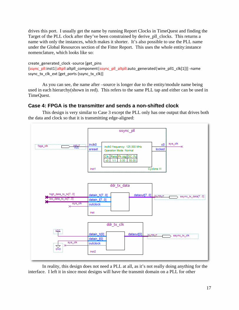
Case 3: FPGA is the transmitter and phase-shifts its clock When transmitting, the user sends the clock and data out through the altddio megafunction:
For Case 3, a second PLL tap is being used to phase-shift the clock 90 degrees. Note that this design uses an altddio_out megafunction for the clock output, and just ties off the ports to VCC and GND. This is not required, but common practice in source synchronous circuits in that it makes the clock path mimic the data path more closely. It also prevents the fitter from sending the clock out the dedicated PLL clock output path, which is not good for source-synchronous timing, since it has considerably different timing than the data output paths. The clock constraints in the .sdc look like so: create_clock -period 8.0 -name fpga_clk [get_ports fpga_clk] derive_pll_clocks create_generated_clock -source [get_pins {inst1|altpll_component|auto_generated|pll1|clk[1]}] -name ssync_tx_clk_ext [get_ports {ssync_tx_clk}]
The first two constraints are pretty straightforward. They constrain the clock coming into the FPGA and then call derive_pll_clocks to constrain the PLL’s outputs. The third constraint puts a generated clock on the output port ssync_tx_clk that sends out the clock, so that it can be used as a clock for our external registers. The –source of the clock is the output of the PLL that
17
drives this port. I usually get the name by running Report Clocks in TimeQuest and finding the Target of the PLL clock after they’ve been constrained by derive_pll_clocks. This returns a name with only the instances, which makes it shorter. It’s also possible to use the PLL name under the Global Resources section of the Fitter Report. This uses the whole entity:instance nomenclature, which looks like so:
create_generated_clock -source [get_pins {ssync_pll:inst1|altpll:altpll_component|ssync_pll_altpll:auto_generated|wire_pll1_clk[1]}] -name ssync_tx_clk_ext [get_ports {ssync_tx_clk}] As you can see, the name after –source is longer due to the entity/module name being used in each hierarchy(shown in red). This refers to the same PLL tap and either can be used in TimeQuest.
Case 4: FPGA is the transmitter and sends a non-shifted clock This design is very similar to Case 3 except the PLL only has one output that drives both the data and clock so that it is transmitting edge-aligned:
In reality, this design does not need a PLL at all, as it’s not really doing anything for the interface. I left it in since most designs will have the transmit domain on a PLL for other
18
reasons, and the generated clock on the clock output will have to use the PLL for its –source option. The .sdc constraints look like so: create_clock -period 8.0 -name fpga_clk [get_ports fpga_clk] derive_pll_clocks create_generated_clock -source {inst1|altpll_component|auto_generated|pll1|clk[1]} -name ssync_tx_clk_ext [get_ports {ssync_tx_clk}] -phase 90 Most of this is pretty straightforward. The generated clock is applied to the output port sending the source synchronous clock off chip and using the PLL as its source. The difference from Case 3 is that this generated clock has added “-phase 90”. Does this –phase do anything to the clock inside the FPGA? No. What this option does is state that the clock being sent off chip will be phase-shifted externally, at the receiver. (I think it would have made more sense to not have a the –phase 90, and instead create a virtual generated clock sourced from this clock going off chip, and put the –phase 90 on this external clock. It is not legal to have virtual generated clocks though, so I have done it this way. The end result is identical.) So the –phase 90 explicitly does nothing to the clock being sent off chip. What it implicitly does is say the external device receiving the data phase-shifts the clock to center it onto the data eye. Knowing the external device does the phase-shift, Quartus II will try to match clock and data delays going off-chip, sending them out edge-aligned.
External Delays of the Explicit Method Now that we’ve set up our clocks to show that there is a phase-shift in the system, we need to apply constraints to the data ports. The designer has already decided if the FPGA is phase-shifting the clock or not, and these external delays will be used to determine how much skew there can be between the data arrival path and data required path, i.e. between the data path and the clock path. For example, when the FPGA is the transmitter, the user will be able to easily say, the data output can leave the FPGA +/-800ps relative to the clock output. This method allows this to be done independently of the phase-shift. So if the FPGA is not phase-shifting the output clock(Case 4), then the data would leave edge-aligned +/-800ps relative to the clock. If the FPGA is phase-shifting the clock going off-chip, then the data would still constrained to be +/-800ps, but the clock would have a 90 degree offset. It’s very nice to be able to separate the data skew from the clock’s phase-shift, as long as you remember it. Cases 2 and 4 are where the FPGA does not phase-shift the clock, and so the skew between data and clock will reflect the physical differences in the FPGA. Cases 1 and 3 will have an additional phase-shift of the clock on top of the skew constraints we are about to enter.
For Case 1 and Case 2, where the FPGA is the receiver, the constraints look like so: set_input_delay -clock ssync_clk_ext -max 0.0 [get_ports {ssync_rx_data[*]}] set_input_delay -clock ssync_clk_ext -min 0.0 [get_ports {ssync_rx_data[*]}] set_input_delay -clock ssync_clk_ext -max 0.0 [get_ports {ssync_rx_data[*]}] -clock_fall -add_delay

19
set_input_delay -clock ssync_clk_ext -min 0.0 [get_ports {ssync_rx_data[*]}] -clock_fall -add_delay
Note that the –max and –min values are 0.0, which is just a placeholder for now. The first two constraints state that there is an external register clocked by ssync_clk_ext that drives data to the FPGA’s ssync_rx_data ports. The last two constraints use the –add_delay to state that there is a second register driving these ports, and –clock_fall states that this second register is clocked on the falling edge of ssync_clk_ext. The circuit described is outside the FPGA, shown in blue:
This covers both Case 1 and Case 2.
For outputs, the constraints look very similar. Once again, the –max and –min values are filled in with 0.0 as a place-holder: set_output_delay -clock ssync_tx_clk_ext -max 0.0 [get_ports {ssync_tx_data[*]}] set_output_delay -clock ssync_tx_clk_ext -min 0.0 [get_ports {ssync_tx_data[*]}] set_output_delay -clock ssync_tx_clk_ext -max 0.0 [get_ports {ssync_tx_data[*]}] -clock_fall -add_delay set_output_delay -clock ssync_tx_clk_ext -min 0.0 [get_ports {ssync_tx_data[*]}] -clock_fall -add_delay The first two constraints say the output ports ssync_tx_data[*] drive an external register clocked by ssync_tx_clk_ext. The last two constraints use the –add_delay to say there is a second external register, and the –clock_fall option says this register is clocked on the falling edge of ssync_tx_clk_ext. This results in the external circuit in blue:

20
Note that Case 3 has the FPGA’s output port ssync_tx_clk driven by a phase-shifted tap of the PLL, while Case 4 has both the data and clock outputs driven by the same tap. The set_output_delay constraints do not care, as they are describing what occurs outside the FPGA. Now that we’ve created our external circuit, it’s time to determine what the external –max and –min values should be.
FPGA-Centric versus System-Centric First off, I wanted to touch on the term FPGA-centric constraints, which tell the FPGA what to do, and System-Centric Constraints, which describe what is going on outside the FPGA. Although this concept can be useful they are also a bit misleading. The constraints set_input_delay and set_output_delay ALWAYS describe what is going on outside the FPGA, and are hence system-centric. That being said, once you state the external delays, you are also ALWAYS constraining the FPGA, and I believe the user should know how they’re constraining the FPGA. So rather than thinking purely in terms of system-centric or FPGA-centric, they really should be thinking of both. The point I believe that is often overlooked is that the system has a setup relationship and hold relationship, which is how the interface meets timing. Part of that relationship will be used by the external delays and part will be used by the FPGA. So when one side is constrained, so is the other. For example, if the setup relationship to an output port is 10ns, then the interface has 10ns to work with. By putting a “set_output_delay –max 3” on the output port, they are stating the external delay is 3ns, but they’re also stating the FPGA has 7ns to work with. When the user knows the setup and hold relationships, it’s easy to see how FPGA-Centric versus System-Centric constraints are really just different sides of the same coin.

21
I am going to concentrate on the FPGA side for the following discussion, since the user should always know what they’re telling the FPGA to do. For example, if the user knows their external receiver has a Tsu of 3ns, they might put in “set_output_delay –max 3”. If the setup relationship is 3.5ns, then they’re giving the FPGA 500ps to work with, but if the setup relationship is 20ns, then they’re giving the FPGA 17ns to work with, which is obviously a big difference. By knowing the setup relationship and hold relationship, as soon as the user says how much of that margin is being used externally, they will know how much they’re leaving for the FPGA. Luckily, the whole premise of the Explicit Clock Shift Method is that the clocks have a 90 degree phase-shift, and hence the setup relationship is +90 degrees and the hold relationship is -90 degrees, and just by knowing the clock period, we know the setup relationship and hold relationship. For example, if the clock period is 8ns, then 90 degrees is 2ns. If the external –max delay is 0.9ns, then the user is saying the FPGA’s data path can be no more than 1.1ns longer than the clock path. Likewise, if the external –min delay is -0.9ns, then the FPGA’s data path can be no less than 1.1ns shorter than the clock path. This is true whether we’re constraining inputs or outputs.
Case 1 and Case 2: FPGA is the Receiver Let’s look at an example set of input constraints, where I have made-up max/min values: set_input_delay -clock ssync_clk_ext -max 0.7 [get_ports {ssync_rx_data[*]}] set_input_delay -clock ssync_clk_ext -min -0.6 [get_ports {ssync_rx_data[*]}] set_input_delay -clock ssync_clk_ext -max 0.7 [get_ports {ssync_rx_data[*]}] -clock_fall -add_delay set_input_delay -clock ssync_clk_ext -min -0.6 [get_ports {ssync_rx_data[*]}] -clock_fall -add_delay
This translates to the following circuits for setup and hold analysis:
Looking at the setup analysis on the left, the relationship between the launch clock and latch clock is 2ns. The external –max delay is 0.7ns. That leaves 1.3ns for the FPGA. That means inside the FPGA, the data delay to the register can be 1.3ns longer than the clock delay and it will still meet timing. On the right side, the hold relationship is -2ns, and the external

22
delay is -0.6ns. That means the data delay inside the FPGA can be 1.4ns shorter than the clock delay and it will still meet timing. In the upcoming report_timing section, we will see this analysis. Now let’s look at a waveform to show the same thing:
The top waveform shows our setup and hold relationships. The bottom waveform shows them superimposed with actual delays. The yellow bars show the external device may skew its data in relation to its clock by +0.7ns to -0.6ns. That leaves the FPGA with +1.3ns and -1.4ns to work with and still meet timing. Using equations: FPGA’s_Data_Delay – Clock_Delay < Setup_Relationship – External_Delay_Max FPGA’s_Data_Delay – Clock_Delay > Hold_Relationship – External_Delay_Min In the Explicit Method, the setup relationship is 90 degrees and the hold relationship is -90 degrees. Using the external delays of 0.7 and -0.6, we get: FPGA’s_Data_Delay – Clock_Delay < 1.3 FPGA’s_Data_Delay – Clock_Delay > -1.4 One point that has been mentioned before but worth bringing up again, is that we’re looking at FPGA skew before analyzing the PLL shift. So in Case 2, where we say the clock-shift occurs externally and therefore clock/data come into the FPGA center-aligned with the data, the clock and data paths will try to maintain that relationship by staying within the required 1.3/-1.4 requirements. Case 1 does the same thing in trying to match the data and clock delays inside the FPGA, but since the clock/data come in edge-aligned, there is an additional 90 degree phase-shift that centers the clock into the middle of the data eye. This is very important not to forget, and easiest to think of skew and phase-shift as two separate things.
Case 3 and Case 4: FPGA is the Transmitter

23
Let’s look at the sample output constraints, with made-up max/min values: set_output_delay -clock ssync_tx_clk_ext -max 1.2 [get_ports {ssync_tx_data[*]}] set_output_delay -clock ssync_tx_clk_ext -min -1.1 [get_ports {ssync_tx_data[*]}] set_output_delay -clock ssync_tx_clk_ext -max 1.2 [get_ports {ssync_tx_data[*]}] -clock_fall -add_delay set_output_delay -clock ssync_tx_clk_ext -min -1.1 [get_ports {ssync_tx_data[*]}] -clock_fall -add_delay This translates to the following circuits for setup and hold analysis:
Looking at the setup analysis on the left, the setup relationship from fpga_clk to ssync_tx_clk_ext is 2ns. The –max external delay is 1.2ns, leaving 0.8ns for the FPGA to deal with. That means the FPGA’s data can come out up to 0.8ns later than the clock comes out and the interface will still make timing. Likewise on the right side, the hold relationship is -2ns, and the external –min delay is -1.1ns, which means the data can come out of the FPGA up to 0.9ns before the clock and the interface will still meet timing. Once again, the question of whether or not the FPGA phase-shifts the output clock is another layer on top of these requirements. For example, if the above constraints were in Case 4, where the FPGA does not phase-shift the output clock, the data output would be constrained within +0.8ns and -0.9ns to the clock output, and hence would be edge-aligned. If the above were used in Case 3, the same would hold true except there would be an additional 90 degree shift on the output clock, making it a center-aligned output. The Explicit Method allows the PLL phase-shift and the data skew to be analyzed separately. And of course the difference between Case 3 and Case 4 is not just how the .sdc constraints are set up. Case 3 physically uses another tap of the PLL with a 90 degree phase-shift to drive the output clock. .

24
Benefits of the Explicit Method There are multiple benefits to the Explicit Clock Shift Method.
- The clock relationships are the same for all cases with a +90° setup and -90° hold relationship, making it easy to understand and analyze all four cases in a similar manner.
- The clock relationships make sense when thinking about the key to source-synchronous timing.
- The default setup and hold relationship are always correct so users don’t have to worry about adding multicycles like the Implicit Method’s next-edge/same-edge transfer.
- Even if the user adds a phase-shift that is not 90 degrees, such as 80 degrees, the default relationships remain correct. See the section on exactly 90 degrees.
- The .sdc setup follows a very cookie-cutter like recipe. - For me, the biggest benefit is that it’s easy to see how the FPGA is being constrained. I
think of it as two layers: 1) How much the data path inside the FPGA can be skewed compared to the clock path.
This is controlled by the equations:
Setup Analysis: FPGA_Data_Delay – FPGA_Clock_Delay < 90° – External_Delay_Max Hold Analysis: FPGA_Data_Delay – FPGA_Clock_Delay > -90° – External_Delay_Min
2) If the clock is phase-shifted inside the FPGA. This is easy to determine since it must
explicitly be done while creating the PLL. It is the combination of these two layers that determine what the FPGA is doing with the data path and clock path.
report_timing: Putting it all together For any FPGA design, I recommend users create a custom Tcl script that analyzes the I/O interfaces(and anything else the user does custom analysis on). I always create a file called TQ_analysis.tcl, and have done so for these designs. The file can be accessed from TimeQuest’s pull-down menu Scripts, so I can analyze the I/O interface any time I want. This is especially useful if doing iterations to get the constraints correct, and hence I want to keep analyzing the same paths over and over. The contents of TQ_analysis.tcl for Case 1 look like so: # Analyze source-synchronous data coming from external clock ssync_clk_ext report_timing -setup -npaths 50 -detail full_path -from_clock {ssync_clk_ext} -panel_name "SSYNC Inputs||setup" report_timing -hold -npaths 50 -detail full_path -from_clock {ssync_clk_ext} -panel_name "SSYNC Inputs||hold" Some quick notes:
- These paths are already constrained and analyzed in TimeQuest. This report just breaks them out into custom reports.

25
- I generally do not add the TQ_analysis.tcl to the Assignments -> Settings -> TimeQuest -> Tcl Script File. The reason is that TimeQuest will then only report what’s in this file and not all the default reports. This behavior should change with Quartus 11.1, in which case I will probably start adding them.
- For I/O analysis, the –detail should be set to full_path, so that the clock tree is broken out into detail. Unlike internal paths, the source clock path and destination clock path are not symmetric and do not cancel out, so the “-detail full_path” is important.
- For I/O, report_timing’s “-from_clock” and “-to_clock” are useful for reporting all paths to/from an external clock. It’s not as necessary for source-synchronous interfaces where the data ports are part of a bus, but for something like a 66MHz PCI bus, where the ports have different names like trdy, irdy, ad[*], stop, perr, serr, etc. it’s easier to report paths based on the single external clock they connect to rather than naming all the individual I/O ports.
- It’s important that the –panel_name option give a good description of the report. And note that the double-pipe || in the panel-name will create a folder in the Report window, which helps organization.
Now let’s look at the timing reports. There are a couple things to analyze.
1) Are the setup and hold relationship correct, i.e. +/- 90 degrees? 2) Is the external delay correct? 3) Is the physical path correct? 4) What is the difference in delays ignoring the relationship and external delay?
Let’s look at the setup report from Case 1:

26
1) The setup relationship is 2ns. This is seen in the top-right, but is also the difference
between the latch edge and launch edge, 6ns – 4ns = 2ns. 2) The external delay is labeled iExt and shown as 0.7ns. That is exactly the
“set_input_delay –max” value from the .sdc. 3) One can follow the Location and Element column to see exactly what is being
analyzed. The Data Arrival Path starts with data ssync_rx_data[0] coming in on Pin_P2, going through the IOIBUF, a combinatorial node LCCOMB, and to the d input of the latching FF at location FF_X1_Y4_N13. The Data Required Path shows the latching clock, which comes in on Pin_E2, going through the IOIBUF, PLL_1, the Global Clock tree CLKCTRL_G3, and finally to the clk port of the latching register at X1_Y4_N13. These are the correct paths inside the FPGA. (Note that the targeted device, Cyclone III, does not have DDR registers in the I/O, which is why the register is in the logic fabric).
4) Ignoring the launch edge time and the iExt, the data path takes 2.220ns to go from the input port to the FF. Ignoring the latch edge time, the clock takes 2.064ns to go from the input port to the FF, for a difference of 156ps. There is also clock uncertainty of -0.060ps and a uTsu of 15ps at the register, which subtract out for a difference of

27
0.201ns. So looking at raw FPGA delays, the data path could be (2.220 – 2.064 + 0.06 – 0.015) = 201ps longer than the clock path. When we add the 700ps external delay, that gets us to 901ps across the interface. Since the requirement is half the data window, or 2ns, we’ve met timing by 2ns – 0.901ns = 1.099ns. That is exactly equal to our slack.
One doesn’t have to do this detailed analysis for every constraint, but the point is that
they can, and they can feel good the numbers add up. If the user is unsure of their constraints or what is being analyzed, I suggest going through this exercise.
I won’t show the hold analysis or any more timing reports, since the user can easily open the specific case projects, compile, launch TimeQuest and run the TQ_analysis.tcl report.
For an output report, here is the setup report from Case 3:

28
1) The setup relationship is 2ns, as it should be. This is seen both at the top-right, and in
the difference of latch edge minus launch edge, i.e. 6ns – 4ns = 2ns 2) The external output delay oExt is -1.2ns. Note that the set_output_delay –max value was
1.2ns, which could be added to the Data Arrival Path, but instead is subtracted from the Data Required Path. I’m not sure why it’s done this way, but it works out the same.
3) The Data Arrival Path starts at input clock fpga_clk on Pin_E2, goes through an IO buffer, PLL, global clock G3, the DDIO cell, the IO buffer and out data port Pin_P2. The

29
Data Required Path comes in on the same clock port, but works its way to the clock output port ssync_tx_clk at Pin_F2. IMPORTANT NOTE: The output clock is constrained with a create_generated_clcok on output port ssync_tx_clk, where the –source is the PLL that drives to that port. I occasionally see designs with an incorrect option for -source, whereby Quartus issues the warning: Warning: No paths exist between clock target "ssync_tx_clk" of clock "ssync_tx_clk_ext" and its clock source. Assuming zero source clock latency.
Besides issuing a warning, the Data Required Path would look like so:
This is wrong, as the path for getting the clock off-chip does not include any of
the delays inside the FPGA. If your design gets this warning, please fix it before looking at anything else, as the timing analysis is not correct. There are two common causes for this. One is specifying the wrong output tap of the clock. For example, the incorrect timing report just shown was created by using Case 3 and specifying the –source of the create_generated_clock as PLL clk[0] instead of clk[1]. Since clk[0] does not actually drive the output port, this problem occurs. The second case is when the output is driven by a ripple clock, i.e. the PLL drives the .clk port of a register before driving the output port.. Clocks do not propagate through registers, and the user must assign a create_generated_clock assignment to each stage of a ripple clock. (If the output clock goes through an altddio_out block, the user does not have to assign a clock to the registers, because the only relevant path is through the mux select, as discussed in the section ”DDR outputs: Where are my registers?”.)
4) Going back to the correct timing report, the final step is to add up the delays. The delays for the data to get off chip occur in the Data Arrival Path, -2.916 + 4.671 = 1.755ns. The delays for the clock to get off chip occur in the Data Required Path, of 1.494ns, minus the clock uncertainty of -110ps, or 1.384ns. The net difference between the data getting out and the clock is 1.755ns – 1.494 + 110ps = 371ps. Next add in the external –max delay of 1.2ns to make it 1.571ns across the interface. Since the setup relationship is 2ns, we make timing by +429ps, which is the reported slack.
Again, one does not have to go through this analysis, but it’s nice to see it once and know how to do it.

30
Section III: The Implicit Clock Shift Method What is the implicit method? Simply put, the implicit method occurs when there is no phase-shift in the interface, and so the clocks are edge-aligned from end to end. Note that if the FPGA phase-shifts the clock as in Case 1 and Case 3, then the user will always use the Explicit Clock Shift Method, as the PLL phase-shift in the FPGA is always explicit. It’s really only Case 2 and Case 4 of the Explicit method that could be done with the Implicit Method. There are two cases where the Implicit method occur.
- One scenario I call the “hidden phase-shift”. This is where the external device does not state it phase-shifts the clock, and instead makes it sound like the delays are phase-shifted. For example, a transmitting device’s datasheet might say that its data is skewed by 1.5ns-2.5ns from the clock. So rather than having a clock shift, the data has a longer output delay. Another example would be a receiving device with a Tsu of 2.5ns and a Th of -1.5ns. When we analyze External Device Constraints, we will look at more examples of this.
- When there really is no phase-shift in the system, and the FPGA must use physical
delays to center the clock edge onto the valid data window. The data and clock paths will no longer have matched delays and this difference will vary over PVT, making the interface run more slowly. The only scenarios where I have seen this occur are when the FPGA is the receiving data edge-aligned with the clock, but the FPGA can’t phase-shift the clock with a PLL. One reason is that the FPGA does not have enough PLLs, and the other reason is that the latching signal is not a clock but a strobe, in which case a PLL can’t be used since it won’t remain locked when the strobe disappears. These are not very common situations, and we will discuss them later in this section.
The first thing to do with the Implicit Method is to set up the clock constraints. That is
really easy, as there is only one way to do it. When the FPGA is receiving, we do:
create_clock -period 8.0 -name ssync_clk [get_ports ssync_rx_clk] derive_pll_clocks create_clock -period 8.0 -name ssync_clk_ext
Note that the external clock and fpga clock are identical. Also note that if there is a PLL inside the FPGA, it does not constraint the clock. Likewise, when the FPGA is the transmitter, the clock constraints are quite straightforward:
create_clock -period 8.0 -name fpga_clk [get_ports fpga_clk] derive_pll_clocks create_generated_clock -source {inst1|altpll_component|auto_generated|pll1|clk[0]} -name ssync_tx_clk_ext [get_ports {ssync_tx_clk}]

31
There really is no need for a PLL in this example, since the clock is not being phase-shifted, but most designs use a PLL anyway. If not, the generated clock on the tx output port would use the input port fpga_clk for its source.
So the clock constraints are easy, but the Implicit Method has a difficult question that needs to be decided by the user that never occurred with the Explicit Method, and is one of the reasons I consider the Implicit Method to be more difficult. Let’s start by looking at the relationships for a DDR interface without a clock-shift:
Since this is DDR, every edge launches data and every subsequent edge latches that data.
This is called a “next-edge” transfer, although nobody really uses that term since it’s just the expected behavior from default analysis. With a setup relationship of 4ns and hold relationship of 0ns, Quartus II will want 2ns added to the data path compared to the clock path, which will have the data arriving midway between the Latch Clock’s setup and hold edges. This will give the optimum setup and hold slack.
But what if it’s better to skew the data -2ns compared to the clock? That would mean we need to shift the setup relationship to 0ns and hold relationship to -4ns, like so:
This is called a “same-edge transfer” because the edge that launches the data is the same
edge that will latch it, i.e. when the rising edge at time 0ns launches data, that same clock edge will have a longer delay to the latching register and hence will be the one to latch it.
So how do we tell TimeQuest this is what we want? The quick answer is to add the following two multicycles:
set_multicycle_path –setup –rise_from [get_clocks {launch_clk}] –rise_to [get_clocks {latch_clk}] 0 set_multicycle_path –setup –fall_from [get_clocks {launch_clk}] –fall_to [get_clocks {latch_clk}] 0
For more details on why, please look at the Implicit Method: Same-Edge Transfers.

32
Note that the projects in Case 5 and Case 6 use the default relationship and hence a next-edge transfer, but the .sdc also has the multicycles that allow for a same-edge transfer, but they are commented out.
Deciding whether to use the next-edge transfer or same-edge transfer will make more sense once we cover the implied phase-shift.
The Implied Phase-Shift For good source-synchronous performance we want to phase-shift the clock somewhere along the interface, yet our clocks are aligned end-to-end. So how does this method get good performance? The key is that the external data delays imply a phase shift. For example, let’s say a receiver said it had a Tsu of 2.5ns and a Th of -1.5ns. There is no mention of a clock-shift and the set_output_delay would have a –max 2.5ns and –min 1.5ns. Taking a step back, remember that there are two variables controlled by the user for I/O constraints, the relationship and the external delay. (Four variables in total, as there is a setup relationship and external –max delay, and hold relationship and external –min delay, but they are analyzed separately). Let’s look at some of the equations we used earlier: Setup Analysis: FPGA_Data_Delay – FPGA_Clock_Delay < Setup_Relationship – External_Delay_Max Hold Analysis: FPGA_Data_Delay – FPGA_Clock_Delay > Hold_Relationship – External_Delay_Min In the Explicit Clock Shift Method, the setup relationship is +90 degrees and the hold relationship is -90 degrees, or +/-2ns for an 8ns clock. Making up terms, let’s say the external –max delay is 0.7ns and the external min delay is -0.6ns, resulting in: FPGA_Data_Delay – FPGA_Clock_Delay < 2 – 0.7 FPGA_Data_Delay – FPGA_Clock_Delay > -2 – (-0.6) Or: FPGA_Data_Delay – FPGA_Clock_Delay < 1.3 FPGA_Data_Delay – FPGA_Clock_Delay > -1.4 Now with the Implicit Method, the default setup relationship is 4 and the default hold relationship is 0. But what if the external delays had 2ns added to both of them for a –max delay of 2.7 and –min delay 1.4. The new analysis would be: FPGA_Data_Delay – FPGA_Clock_Delay < 4 – 2.7 FPGA_Data_Delay – FPGA_Clock_Delay > 0 – 1.4 Or: FPGA_Data_Delay – FPGA_Clock_Delay < 1.3 FPGA_Data_Delay – FPGA_Clock_Delay > -1.4

33
As you can see, the FPGA is constrained in the exact same manner, where the
(FPGA_Data_Delay – FPGA_Clock_Delay) must be less than 1.3ns and greater than -1.4ns. Remember that the FPGA is NOT phase-shifting the clock. In the Explicit Method, we say that the external device is phase-shifting the clock, which affects our setup and hold relationship. In the Implicit Method we do not say it phase-shifts the clock, and instead state that the external device’s delays are “shifted”. If we want to subtract 90 degrees from the data delays, then we need to add multicycles to tell TimeQuest to use the same-edge transfer setup and hold relationships of 0 and -4. The external delays would also be shifted by -2ns to 0.7 – 2 = -1.3ns and -0.6 – 2 = -2.6ns. That allows us to do:
FPGA_Data_Delay – FPGA_Clock_Delay < 0 – (-1.3) FPGA_Data_Delay – FPGA_Clock_Delay > -4 – (-2.6) Or: FPGA_Data_Delay – FPGA_Clock_Delay < 1.3 FPGA_Data_Delay – FPGA_Clock_Delay > -1.4 As can be seen, I call this the Implicit Clock Shift because the data delays have been shifted by -2ns instead of having the clock shifted. We know there needs to be a clock phase-shift in the system to get optimal timing. The explicit method clearly shows that shift in the clock relationships while the implicit method keeps the clocks aligned and instead shifts the external delays by +/-90 degrees. A quick rule of thumb is if the external delays are symmetric around 0, such as a max of 0.5 and min of -0.5, then the explicit method is being used. If they have an offset near 90 degrees, such as a max of 2.5 and min of 1.5, then the Implicit Method is being used with the default setup and hold relationships. If they have a -90 degree offset, such as a max of -1.5 and min of -2.5, then they are using the Implicit Method and need multicycles to specify a same-edge transfer. Why have all these methods? The main reason is to allow users to properly describe the external device, and there will be examples in the External Devices Constraint Examples.
Case 5 : FPGA is Receiver, Implicit Method The Case 5 design is identical to Case 2 except for the .sdc. The FPGA is receiving source synchronous data, the FPGA is not phase-shifting the clock. The only difference is how we describe the external world. Using the Explicit Method in Case 2, the external device phase-shifted the clock 90 degrees and the external delays described how much skew there was from the external device. The .sdc in Case 5 does not phase-shift the external clock, but instead adds 2ns to the external delays. There is also another solution commented out, where the external delays have 2ns subtracted from them and multicycles are added to tell TimeQuest it is transferring data to the previous edge. Let’s look at them side-by-side, with major differences in red:

34
Case 2 ssync_test.sdc Setup Relationship = 2ns, Hold Relationship = 2ns create_clock -period 8.0 -name ssync_clk [get_ports ssync_rx_clk] derive_pll_clocks create_clock -period 8.0 -name ssync_clk_ext –waveform {6.0 10.0} set_input_delay -clock ssync_clk_ext -max 0.7 [get_ports {ssync_rx_data[*]}] set_input_delay -clock ssync_clk_ext -min -0.6 [get_ports {ssync_rx_data[*]}] set_input_delay -clock ssync_clk_ext -max 0.7 [get_ports {ssync_rx_data[*]}] -clock_fall -add_delay set_input_delay -clock ssync_clk_ext -min -0.6 [get_ports {ssync_rx_data[*]}] -clock_fall -add_delay Case 5 ssync_test.sdc – Default setup and hold Setup Relationship = 4ns, Hold Relationship = 0ns create_clock -period 8.0 -name ssync_clk [get_ports ssync_rx_clk] derive_pll_clocks create_clock -period 8.0 -name ssync_clk_ext set_input_delay -clock ssync_clk_ext -max 2.7 [get_ports {ssync_rx_data[*]}] set_input_delay -clock ssync_clk_ext -min 1.4 [get_ports {ssync_rx_data[*]}] set_input_delay -clock ssync_clk_ext -max 2.7 [get_ports {ssync_rx_data[*]}] -clock_fall -add_delay set_input_delay -clock ssync_clk_ext -min -1.4 [get_ports {ssync_rx_data[*]}] -clock_fall -add_delay Case 5 ssync_test.sdc – Multicycle setup and hold: Setup Relationship = 0ns, Hold Relationship = 4ns create_clock -period 8.0 -name ssync_clk [get_ports ssync_rx_clk] derive_pll_clocks create_clock -period 8.0 -name ssync_clk_ext set_multicycle_path -setup -rise_from [get_clocks {ssync_rx_clk}] -rise_to [get_clocks {inst1|altpll_component|auto_generated|pll1|clk[0]} 0 set_multicycle_path -setup -fall_from [get_clocks {ssync_rx_clk}] -fall_to [get_clocks {inst1|altpll_component|auto_generated|pll1|clk[0]} 0 set_input_delay -clock ssync_clk_ext –max -1.3 [get_ports {ssync_rx_data[*]}] set_input_delay -clock ssync_clk_ext -min -2.6 [get_ports {ssync_rx_data[*]}] set_input_delay -clock ssync_clk_ext -max -1.3 [get_ports {ssync_rx_data[*]}] -clock_fall -add_delay set_input_delay -clock ssync_clk_ext -min -2.6 [get_ports {ssync_rx_data[*]}] -clock_fall -add_delay These three methods constrain the FPGA identically. I ran place-and-route of Case 5 and then ran TimeQuest with the different .sdc files. Below are the setup reports, and you’ll see that the slack is identical. The only thing that changes is the Setup Relationship(which is Launch Edge – Latch Edge) and the iExt delay, which is from the .sdc’s set_input_delay –max:

35
So if the three methods are identical, which one do we use? It really depends on how the user wants to describe their external device. We’ll cover this more in the External Device Examples, but here’s a quick example. Case 2 ssync_test.sdc – This could be used if the external transmitter said it was sending the clock center-aligned and its data could vary by +0.7ns to -0.6ns. Case 5 ssync_test.sdc, Default Relationships – This could be used if the external transmitter said it was sending source-synchronous data, and the data would transition between 1.4ns to 2.7ns AFTER the clock. Case 5 ssync_test.sdc, Multicycle – This could be used if the external transmitter said it was sending source-synchronous data, and the data would transition between 1.3 to 2.6ns BEFORE the clock(i.e. the data to clock skew would be -1.3 to -2.6).
Case 6 : FPGA is Transmitter, Implicit Method The design in Case 6 is identical to Case 4 in that the FPGA is transmitting source-synchronous clock and data and does not phase-shift the clock. The only differences are in the .sdc constraint. The first difference is that we do not say the external clock is phase-shifted by removing the –phase option from the create_generated_clock constraint. This makes the default setup relationship 4ns and the default hold relationship 0ns. Next, we add 2ns to the external delays. The .sdc has a second option that is commented out, whereby multicycles are used to state that the FPGA is latching data on the same edge that launches it. This results in a setup relationship of 0ns and a hold relationship of -4ns. The external delays are then shifted by -2ns. Summarizing the three options: Case 4 ssync_test.sdc Setup Relationship = 2ns, Hold Relationship = 2ns create_clock -period 8.0 -name fpga_clk [get_ports fpga_clk]

36
derive_pll_clocks create_generated_clock -source [get_pins {inst1|altpll_component|auto_generated|pll1|clk[0]}] -name ssync_tx_clk_ext [get_ports {ssync_tx_clk}] -phase 90 set_output_delay -clock ssync_tx_clk_ext -max 1.2 [get_ports {ssync_tx_data[*]}] set_output_delay -clock ssync_tx_clk_ext -min -1.1 [get_ports {ssync_tx_data[*]}] set_output_delay -clock ssync_tx_clk_ext -max 1.2 [get_ports {ssync_tx_data[*]}] -clock_fall -add_delay set_output_delay -clock ssync_tx_clk_ext -min -1.1 [get_ports {ssync_tx_data[*]}] -clock_fall -add_delay Case 6 ssync_test.sdc – Default setup and hold Setup Relationship = 4ns, Hold Relationship = 0ns create_clock -period 8.0 -name fpga_clk [get_ports fpga_clk] derive_pll_clocks create_generated_clock -source [get_pins {inst1|altpll_component|auto_generated|pll1|clk[0]}] -name ssync_tx_clk_ext [get_ports {ssync_tx_clk}] set_output_delay -clock ssync_tx_clk_ext -max 3.2 [get_ports {ssync_tx_data[*]}] set_output_delay -clock ssync_tx_clk_ext -min 0.9 [get_ports {ssync_tx_data[*]}] set_output_delay -clock ssync_tx_clk_ext -max 3.2 [get_ports {ssync_tx_data[*]}] -clock_fall -add_delay set_output_delay -clock ssync_tx_clk_ext -min 0.9 [get_ports {ssync_tx_data[*]}] -clock_fall -add_delay Case 6 ssync_test.sdc – Multicycle setup and hold: Setup Relationship = 0ns, Hold Relationship = 4ns create_clock -period 8.0 -name fpga_clk [get_ports fpga_clk] derive_pll_clocks create_generated_clock -source [get_pins {inst1|altpll_component|auto_generated|pll1|clk[0]}] -name ssync_tx_clk_ext [get_ports {ssync_tx_clk}] set_output_delay -clock ssync_tx_clk_ext -max 3.2 [get_ports {ssync_tx_data[*]}] set_multicycle_path -setup -rise_from [get_clocks {inst1|altpll_component|auto_generated|pll1|clk[0]}] -rise_to [get_clocks {ssync_tx_clk_ext}] 0 set_multicycle_path -setup -fall_from [get_clocks {inst1|altpll_component|auto_generated|pll1|clk[0]}] -fall_to [get_clocks {ssync_tx_clk_ext}] 0 set_output_delay -clock ssync_tx_clk_ext -max -0.8 [get_ports {ssync_tx_data[*]}] set_output_delay -clock ssync_tx_clk_ext -min -3.1 [get_ports {ssync_tx_data[*]}] set_output_delay -clock ssync_tx_clk_ext -max -0.8 [get_ports {ssync_tx_data[*]}] -clock_fall -add_delay set_output_delay -clock ssync_tx_clk_ext -min -3.1 [get_ports {ssync_tx_data[*]}] -clock_fall -add_delay These three methods constrain the FPGA identically. I ran place-and-route of Case 6 and then ran TimeQuest with the different .sdc files. Below are the setup reports, and you’ll see that the slacks are almost identical. The setup relationship(which is Launch Edge – Latch Edge) and the oExt delay change in each case, but in a way that cancels the other out. Here is the setup analysis with each set of constraints:

37
Note that the middle analysis has 3ps more slack than the other two. I won’t go into much detail, but this is due to rise-fall variation in the clock tree. It only occurs when the FPGA is the transmitter because it has both the launch clock and the latch clock inside the FPGA, and so changing which edge data is captured on will change which rise/fall models are compared. It can be seen in the section +/-90 degrees?
Really, the Interface Has No Clock Shift Another scenario is when there really is no phase-shift of the clock and there is no implied phase-shift. One scenario I have seen this is when receiving edge-aligned clock/data, but the FPGA has run out of PLLs to phase-shift the incoming clock 90 degrees. Note that one solution to this scenario is to use Dynamic Phase-Alignment(DPA), which allows one PLL to clock in data from multiple interfaces, assuming they all run off the same base clock. Another scenario where this occurs is when the FPGA is again receiving edge-aligned clock/data, but rather than a real clock, the latching signal is a strobe. Even if a PLL is available, it can’t be used since it won’t lock onto a strobe, and hence there is no way to shift the strobe 90 degrees in a way that won’t vary over PVT. Both of these situations are constrained in the same manner. Note that I’ve grouped this under the Implicit Phase-Shift Method since the clocks are edge-aligned, but in this scenario the phase-shift isn’t implicit, it just doesn’t exist at all. I didn’t want to create another “method”, since this is constrained just like the implicit shift method. Sorry for any confusion. (I also tried many different names for the two methods, but felt Explicit Clock Shift and Implicit Clock Shift really were the best…) So in this case, the external device is transmitting its data and clock edge-aligned, but the FPGA does not or cannot use a PLL to phase-shift the incoming clock 90 degrees. As mentioned, having someone phase-shift the clock is the key to source-synchronous performance,

38
so the interface will not be able to run as fast under these conditions, but slower interfaces will often still close timing, which means the interface will work. The first question in this scenario is if Quartus II should add 2ns to the data path compared to the clock path(default relationships) or subtract 2ns of delay compared to the clock path(multicycle relationships). Physically, the data input directly drives a register and can be very fast. The clock comes in on a different I/O port and must route, either through a global clock tree or local routing, to the latch register. So just looking at the paths, the data path will naturally be shorter than the clock path. Because of this, the best solution is to tell Quartus II to skew the data by -2ns compared to the clock path. As shown at the beginning of this section, this can be achieved with multicycles. I did not create a separate case for this scenario. It is basically the same design as Case 5, and the same .sdc. The only difference is that:
- There is no PLL in the actual design. - Use the second set of output constraints that are commented out. They have the
multicycles in front of them, which look like so. (Note that I changed the clock in the –rise_to option, since the PLL is not used.
- set_multicycle_path –setup –rise_from [get_clocks { ssync_clk_ext}] –rise_to [get_clocks { ssync_rx_clk}] 0 set_multicycle_path –setup –fall_from [get_clocks { ssync_clk_ext}] –fall_to [get_clocks { ssync_rx_clk}] 0
- The significant difference is that the –max and –min values will not be offset and
instead will be symmetrical. For example, they might be something like: set_input_delay -clock ssync_clk_ext -max 0.9 [get_ports {ssync_rx_data[*]}] set_input_delay -clock ssync_clk_ext -min -0.9 [get_ports {ssync_rx_data[*]}] set_input_delay -clock ssync_clk_ext -max 0.9 [get_ports {ssync_rx_data[*]}] -clock_fall -add_delay set_input_delay -clock ssync_clk_ext -min -0.9 [get_ports {ssync_rx_data[*]}] -clock_fall -add_delay The net sum is that we’re saying the external device is sending its data and clock edge-aligned, and the data is skewed +/-0.9ns externally. Due to the multicycle, the Quartus II will try to make the FPGA’s data delays 2ns shorter than the clock delay, but can be off by +/- 1.1ns.
Section IV: SDR – Single Data Rate I have gone into great detail showing the various cases for DDR interfaces. For interfaces that run at Single-Data Rate(SDR), I will instead explain the differences from DDR. Note that SDR projects for each case exist in the projects .zip file, and can be found under the directory /SDR. The clock rate was doubled in each case to 250MHz, which is reflected both in the PLL megafunction and the associated .sdc files. Note that there are a few major differences between SDR interfaces and DDR interfaces, and most of them make SDR easier.
- No worrying about rising and falling edges. Because of this, things like “False Paths for Loose Requirements” don’t occur at all, and when doing a multicycle to get “Same Edge Transfers with the Implicit Method”, the multicycle doesn’t have to worry about rise/fall edges in the constraint and can be something simple like:

39
set_multicycle_path –setup –from [get_clocks {launch_clk}] –to [get_clocks {latch_clk}] 0
- Everything will be 180° instead of 90°. For example, when using the explicit method, the clock will be shifted by 180°, making the setup and hold relationships +/-180°. Basically the data window is twice as big, because the data rate is half that of DDR.
- The only thing about SDR that could be considered more difficult, is that the user has more ways to center the clock onto the data eye. They can do a PLL phase-shift, just like with DDR, but launching/latching data on the falling edge of the clock is pretty much the same thing as a 180° shift. This just gives the user more options. Internally, TimeQuest knows when a register is clocked on a falling edge and will change the edge time accordingly, so the user does not have to do anything special. The only corner case that we’ll discuss is when transmitting a clock off-chip and inverting it on the way out. In this case, the user must tell TimeQuest about the inversion.
I am going to cover the six cases very quickly, mainly pointing out how these cases differ
than the DDR cases that were analyzed in detail.
The SDR Explicit Method The Explicit Method still involves making sure the clock is centered on the data eye
somewhere in the FPGA. The major difference is that this centering might not only occur with a PLL phase-shift, but could also be a register clocked on the falling edge of the clock. This results in a setup relationship of 180° and a hold relationship of -180°.
Case 1: The FPGA is the receiver and centers the clock A user might think, now that the clock can be centered by clocking data in on the falling
edge, they no longer need a PLL. But when the FPGA is the receiver, a PLL is still recommended. The reason is that a source-synchronous interface works on the concept that the data delay to the register matches the clock delay. Inside the receiving FPGA, the data path goes from an input port directly to the register in the I/O cell, which is very fast. A clock comes in an I/O port and generally gets on a global clock tree and makes its way to the I/O register. This path is considerably longer and slower than the data path. A PLL in source-synchronous compensation mode will compensate for this clock tree and make the clock path look much more similar to the data path. So for high speeds, a PLL is still necessary.
In the accompanying project /SDR/Case_1, I still use a PLL in Source-Synchronous Compensation Mode, but the output clock was modified from a 90° phase-shift to 180°. Since the clock period is 4ns, this gives us our 2ns setup relationship and -2ns hold relationship. Everything else in the project is pretty much the same. The other benefit of using a PLL is that the user can modify it from 180° in case they need more margin on setup or hold, which can’t be done with a clock inversion.
Another option would be to not phase-shift the output clock, and instead clock the input register on the falling edge. If the user made that modification to the design, there would not need to be any changes to the .sdc. The only major difference is that the path from the I/O register to the next register in the design, which I assume is clocked on the positive edge, would only have a half-cycle to make the transfer.

40
Finally, a user may not have access to a PLL, and only wants to use the clock inversion. This is certainly possible at lower speeds, it just won’t work at the very limits of the device, since the data path and clock path will now have different delays to the register. Most devices have input delay chains that Quartus II will automatically increase to try and match the clock tree delay, but it generally won’t be as good as using a PLL. I’ve found many SDR interfaces to run at slower speeds(say 150MHz as a rough ballpark), which often work fine without a PLL, but it needs to be determined by the designer. Again, if the user modifies the accompanying project to not use a PLL, they do not have to make any changes to the .sdc.
Case 2: The FPGA is the receiver and does not center the clock Just like Case 1, a PLL is still recommended to balance the data and clock paths inside the receiving FPGA and achieve the highest performance, but again like clock 1, a PLL may not be necessary at lower speeds. Since the FPGA is not centering the clock onto the data eye, the key to case 2 is to tell TimeQuest that the external device is doing this. The example .sdc in /SDR/Case_2 does this by stating the clock coming into the FPGA has a 180 degree phase-shift compared to the external clock. This is done with the –waveform option stating the first rising edge is at 2ns instead of the default 0ns: create_clock -period 4.0 -name ssync_rx_clk [get_ports ssync_rx_clk] -waveform {2.0 4.0} create_clock -period 4.0 -name ssync_clk_ext Also like the DDR Case 2, there are multiple ways to do this. The most common would be to shift the external clock instead of the clock coming into the FPGA. It’s easiest to think of achieving this with a -180° shift on the external clock, but the create_clock command does not allow for negative shifts. Instead it is achieved by doing a +180° shift. Since clocks are periodic, TimeQuest will achieve the same setup and hold relationship whether or not the external clock is shifted +180° or -180°. The way to express this is with the positive waveform shift: create_clock -period 4.0 -name ssync_rx_clk [get_ports ssync_rx_clk] create_clock -period 4.0 -name ssync_clk_ext -waveform {2.0 4.0} The above two sets will give identical relationships, so it is whatever the user is most comfortable with.
Case 3: FPGA is the transmitter and phase-shifts its clock For SDR interfaces, there really is no need for a PLL to improve performance, but I have left it in since I find most designs are using a PLL, and it’s important to show the create_generated_clock assignment on the output clock port in relation to a PLL tap. So how did I shift the output clock into the center of the data eye? This was achieved by sending the clock through an altddio_out megafunction, but inverting the data inputs so the data_h signal is tied to GND and the data_l signal is tied to VCC. This inverts the clock as it

41
goes off chip. Note that TimeQuest does not recognize this as an inversion, and so the user MUST put the –invert option on the create_generated_clock assignment. If they do not do this, TimeQuest will not think the output clock is inverted. Please read the upcoming Case 4 section for a comparison. Because SDR has more options, a user could just as easily invert the output clock and not use the altddio_out megafunction. This is perfectly acceptable, but the user must still add the –invert option to the output clock. A final option is to use a second tap of the PLL to drive the output clock and to phase-shift it 180° degrees. In this case the user does not add a –invert option to the generated output clock, since TimeQuest is aware of the 180° shift in the PLL. The downside to this method is that it uses another output of the PLL and another clock tree just to get the clock out. The upside is that the user could shift the clock to other values, such as 160° or 200°, allowing them to trade margin between the setup and hold relationships.
Case 4: FPGA is the transmitter and sends a non-shifted clock Case 4 also does not require a PLL, but I have left it in there since most designs have it anyway. This example sends the clock and data out edge-aligned, using the same clock and without any inversion. For the Explicit Method, the key to sending data and clock edge-aligned is to say that the clock is centered onto the data eye at the far end. We achieve this by adding the –invert option to the create_generated_clock assignment on the output clock. (We could have also done a –phase 180 and gotten identical results). By saying the clock is centering the clock into the data eye by inverting it at the receiving device, the transmitting FPGA should keep them as closely aligned as possible. We did the same thing with the DDR example. Note that Case 3 and Case 4 have .sdc constraints that are dangerously close. In Case 3, we physically invert the clock going off chip, but have to add the –invert option because TimeQuest does not recognize the inversion. In Case 4, we explicitly do not invert the clock going off chip, but use the –invert option to say that the external receiving device is doing the inversion. In both cases, we’re telling TimeQuest to match the data and clock output delays as closely as possible excluding the inversion. Case 3 does the inversion inside the FPGA and sends the clock and data center-aligned, while Case 4 does not invert the output clock inside the FPGA, and so sends them edge-aligned. If the user forgot to do the –invert in either case, Quartus would see a setup relationship of 360° and a hold relationship of 0°. In order to get the most slack for setup and hold, Quartus would try to add 180° worth of delay to the output data path in relation to the output clock path, which is exactly what we do not want in a source-synchronous interface. (Although we will see this done with the Implicit Method…)
The SDR Implicit Method The Implicit Method was discussed in detail for the DDR examples, and so here I will mainly cover any changes. This method is still only valid when the FPGA does not center-align the clock, and hence can only be used in lieu of Case 2 and Case 4. Note that we still end up with a default setup relationship of +360° and a hold relationship of 0°, because there is no phase-shift/inversion across the interface. Instead, the set_input_delay or set_output_delay

42
constraints are shifted in a way that accounts for a phase-shift, so that the fitter will still try to match the data and clock paths into or out of the FPGA. There is also still the option of doing a same-edge transfer, which can be achieved by adding a set_multicycle_path –setup 0 between the external clock and internal clock. Both example projects in /SDR/Case_5 and /SDR/Case_6 show this option commented out. The difference from DDR is that this same-edge transfer can be achieved with just a single multicycle assignment, and the user can just use –from/-to to specify the clocks, without worrying about –rise_from/-fall_from/-rise_to/-fall_to.
Case 5 : FPGA is Receiver, Implicit Method Just like the Explicit Method, a PLL is still recommended when receiving data, since it can compensate for the long clock tree and make it look more like the data path, hence matching the internal clock/data delays. For slower interfaces, a PLL may not be necessary. There really are no tricks tricks to this example. The PLL is in source-synchronous compensation mode and is used to drive the input register. Since the external clock and internal clock are edge-aligned, the user will have a +360° setup relationship and 0° hold relationship with the default next-edge transfer. The key here is the same as with DDR, that the external delays are shifted to a positive bias, which would be close to +180°. In the example /SDR/Case_5, the clock period is 4ns and the set_input_delay constraints have a –max 2.7 and –min 1.4, which is 700ps and 600ps away from the mid-point of 2ns. (I didn’t make them identically different since many external devices don’t have perfectly symmetric relationships anyway).
Case 6 : FPGA is Transmitter, Implicit Method The PLL is optional for this case, but I left it in since most designs will be using a PLL anyway. The clock is sent out through an altddio_out megafunction, which is implemented in the I/O cell and hence matches the SDR output register. There really is nothing special about this case besides it using the Implicit Method, whereby the setup relationship is 360° and the hold relationship is 0°. The user also has the option to do a same-edge transfer, resulting in a 0° setup relationship and a -360° hold relationship.
Section V: Miscellaneous Topics
Edge-Aligned versus Center-Aligned The terms edge-aligned and center-aligned get used commonly when referencing source-synchronous interfaces. The common definition I hear is that edge-aligned means the clock and data transition at the same time, and center-aligned means the clock edge has been shifted onto the center of the data eye. That’s all good, except it doesn’t say at what point in the interface. As discussed, the whole key to source synchronous interfaces is that somebody phase-shifts the

43
clock into the middle of the data eye. If they were edge-aligned from beginning to end, the clock and data would change at the same time in the latching register, and the interface would fail. A more rigorous definition that aligns with most usage is that edge-aligned and center-aligned refer to the relationship at the board, between the two devices. Based on that, these terms refer to how the clock and data leave the transmitter. The receiver can actually be thought of as the opposite, i.e. if the transmitter sends data edge-aligned, then it’s up to the receiver to shift the clock and center-align it. Conversely, if the transmitter sends the clock and data center-aligned, then it us up to the receiver to maintain that alignment. I stay away from edge-aligned/center-aligned for that reason, in that TimeQuest is looking at the whole interface. I do use the terms occasionally, but try to keep to the more rigorous definition. One other note is that some standards don’t even fit that mold. For example, triple-speed ethernet’s RGMII spec states that neither the transmitter or receiver phase-shifts the clock, but instead the user adds 90 degrees of trace delay on clock’s board routing. So the clock and data leaves the transmitter edge-aligned but enters the receiver center-aligned. The spec has been updated to allow for one of the devices to phase-shift the clock, which is what most interfaces do.
Output Clock is Unconstrained Running TimeQuest’s task “Report Unconstrained Paths” on designs where the FPGA is the transmitter shows the following:
The comment does nicely state that the port driving out the source-synchronous clock has a clock assignment, but it still shows up as unconstrained. The reason is that there are not constraints to say how quickly or shortly the clock must get off chip. I am trying to get this behavior changed so the output port doesn’t show up at all. A nice corollary is all input clock ports, which only have a clock constraint on them, are not considered unconstrained. The user can deal with this a few ways:
1) Ignore it – I do this, and many designers may not have even noticed this if it weren’t brought up. But I do understand that some designers/companies try not to ignore messages, since it opens Pandora’s Box of what can and cannot be ignored. Of course, we manage to get by with the many warnings out of Quartus II…
2) Cut timing to the port:
# The following false path removes this port from showing up in the Unconstrained Paths: set_false_path –to [get_ports ssync_tx_clk]
This is a good option, as it removes the path from the Unconstrained Paths report, but
allows it to be used as a clock for output delay analysis. 3) Put a loose constraint on the port, such as:
set_max_delay –to [get_ports ssync_tx_clk] 100

44
set_min_delay –to [get_ports ssync_tx_clk] -100 I do not recommend this, since Quartus II tries to get the optimal setup and hold slack on
I/O ports. That means it could theoretically try to add/remove delay from the clock path just to get more slack, which could then alter the source-synchronous timing. I’ve run a test design and don’t see this happening, but it is a concern. There is no reason to have unnecessary requirements on a clock that may affect timing on other parts of the design.
False Paths for Loose Requirements A lot of TimeQuest documentation and examples on-line will have false paths on their DDR interfaces. The reason is to cut timing on register transfers that don’t occur. For example, I may draw the setup and hold relationships like so:
But that only covers half the transfers. Just showing all of them from the rising edge register, the relationships looks like so:
There are another four arrows that should be drawn from the falling edge at time 4ns, but I didn’t draw them because of the clutter. These transfers exist because the rising edge register drives two latching registers, one clocked on the rising edge and one clocked on the falling edge. The BOLD arrows indicate the falling-edge latch register’s setup relationship of 6ns and hold relationship of -2ns. The thin arrows indicate the rising-edge latch register’s setup relationship of 2ns and hold relationship of -6ns. The reason my previous waveform only showed the setup of 2ns and hold of -2ns is that they are the more restrictive requirements, and if the interface meets those, it automatically meets the outer relationships of +6n and -6ns. This all can be see by looking further down the report_timing analysis of a DDR interface:

45
This is the setup report on an 8-bit DDR input. There are 16 paths analyzed that barely meet timing by just over 1n and are our critical paths, but staring at row 17, there are another 16 paths(not all shown) that all easily meet timing. The Data Delay and Clock Skew on these paths did not materially change, it’s just that the setup relationship jumped from 2ns to 6ns, increasing the slack by 4ns. A lot of TimeQuest documentation and examples show how to cut these extra paths. The basic method I do for this is to draw out all the transfers and set a false path on the outer ones based on the rise/fall relationship. For example, the above timing waveform would have the following constraints: set_false_path –setup –rise_from [get_clocks launch_clk] –fall_to [get_clocks latch_clk] set_false_path –hold –rise_from [get_clocks launch_clk] –rise_to get_clocks latch_clk] set_false_path –setup –fall_from [get_clocks launch_clk] –rise_to [get_clocks latch_clk] set_false_path –hold –fall_from [get_clocks launch_clk] –fall_to [get_clocks latch_clk] The second two constraints cut the looser requirements from the falling edge launch register. As you can see, this is complicated. And if something changes, such as the latch clock is shifted -90 degrees instead of +90 degrees, all the false paths need to be switched. So what do these false paths help? Not much. They clean up the timing report a bit, but their requirements are always looser than the real requirements and therefore never drive the fitter. What happens if the false paths are entered incorrectly? The user ends up cutting real paths that need to be analyzed. I have twice seen designs do this. (In both cases we found we were still meeting the tighter requirements once we removed the false paths, so it didn’t cause a problem, but it could have and we would have never known.) My feeling is that designs don’t have a lot to gain from entering these false paths and a lot to lose, not just from entering them incorrectly but from time spent figuring them out and the extra clutter in the .sdc file. So though there is nothing wrong with having these false paths in a design when they are entered correctly, my suggestion is to just leave them out.

46
Differing Rise/Fall Transfers: +90° versus -90° Clock Shifts, Next-edge versus Same-Edge Transfers For the Explicit Method, I pretty much always show the waveform where the Latch Clock is shifted +90 degrees(the Launch Clock could also be shifted +270 degrees, as it would be the same thing due to clock periodicity). The waveform looks like so:
But what if the launch clock were shifted +90 degrees(or the latch clock shifted +270 degrees, which is the same thing due to clock periodicity)? The waveform would look like so:
The setup relationship is still 2ns and the hold relationship is -2ns. So does this have any affect at all? I would say no, but there are a few minor things to point out:
1) If doing the False Paths for Loose Requirements, then the user must change the orientation of their –rise_from/-fall_from/-rise_to/-fall_to transfers that are being cut. This is very important, but if the user follows my recommendation to not put a false path on these to begin with, it won’t matter.
2) If the external device is constrained with different rise/fall times, then this will make a difference. The set_input_delay and set_output_delay constraints have –rise/-fall options, allowing the user to enter different –max/-min values for both –rise and –fall. I have NEVER seen this done.
3) When the FPGA is transmitting, part of the launch clock and latch clock paths are inside the FPGA, and TimeQuest has different models for rise and fall times. So changing these will affect timing. I did a test-case though, and found a difference of only 3ps on my design.
Beyond those corner cases, the symmetries involved with DDR interfaces and the periodicity of clocks generally make a +90 degree shift get analyzed the same way as a -90 degree shift.
For the Implicit Method, the next-edge transfer and same-edge transfer have similar rise/fall differences:

47
As a result, they are subject to the same three affects listed above(which are generally
negligible).
Exactly 90°? Are phase-shifts always going to be exactly 90 degrees? The answer quite often is no. When external devices shift their clock, they often don’t do it by exactly 90 degrees. Likewise devices that don’t shift their clock often give non-symmetric skew on their data, so centering the clock might require more or less than a 90 degree shift. For example, a transmitter sending data with an 8ns clock would have a symmetric output if the clock was skewed from the data between 1.5-2.5ns. In essence, this can be thought of as a 2ns shift, and the data is changing by +/-500ps. But let’s say the datasheet said the skew was 1.4- 2.4ns. This is really like a 1.8ns skew with the data +/-400ps around that. So the clock is shifted 1.8ns instead of the ideal 2.0ns. Another example is if the external device is phase-shifting the clock but doesn’t do it exactly 90 degrees. How do you handle this? Unless it’s significantly off, my first recommendation is to not worry about it. The 90 degree shift isn’t magical in that it works and anything else does not. Quartus II will generally just add/remove delay chain settings in the I/O to compensate for the difference, and if it’s a small change, the user probably won’t even notice. I would really only try to compensate if it’s quite a bit off(say the external device is doing a 60 degree shift) and you don’t meet timing. How to change the shift depends on which method is being used. Explicit Clock Shift Method When using the explicit clock shift, it is quite easy to shift the clock a little more or less and not have any consequences. Looking at a waveform where the latch clock is a little more than 90 degrees:

48
This works whether the launch clock or latch clock is shifted. It also works if the FPGA is phase-shifting the clock or not. For example, let’s say we’re doing Case 2, where the external device phase-shifts the clock, except it is only a 75 degree shift. There is no reason the user’s PLL couldn’t do another 15 degree shift on top of that. The constraints would show the external clock coming into the FPGA with a 75 degree shift, and then the PLL would do another 15 degree shift which would be constrained with derive_pll_clocks. Implicit Clock Shift Method The implicit shift method is more complex because the launch and latch clock edges are aligned. The TimeQuest User Guide’s “Phase-Shift affect on Setup and Hold” discusses how small shifts on edge-aligned clocks can have big affects on setup and hold. Remember that the Implicit Method only applies when the external device is phase-shifting the clock, since having the FPGA shift the clock is always explicit. This topic only comes into play when the external device isn’t quite phase-shifting 90 degrees and the user wants to have the FPGA shift the clock a little more. There are a few scenarios to deal with. First is if the user is doing a next edge transfer:

49
The top waveform is our default relationship with no PLL shifts, showing a transfer to the next edge.
The middle waveform shows what happens if the Latch edge is shifted forward by -.2ns. The next edge transfer is still intact and the setup relationship decreases to 3.8ns and the hold relationship also decreases to -0.2ns. A case where this might occur is when the FPGA is transmitting edge-aligned, but another tap of the PLL is used to shift the launch clock(which controls the data) forward a bit. The bottom waveform is also a next-edge transfer, but the Latch clock is shifted forward by 0.2ns. This causes the setup and hold relationships to change by a cycle, and so a multicycle is necessary to get the desired result. This can occur when the FPGA is receiving and the user wants to shift the incoming clock a little bit, or when transmitting and they use another tap of the PLL to shift the outgoing clock a little bit. The next scenario involves same edge capture, which requires a multicycle to begin wth:

50
So the first waveform is a same-edge transfer, and requires the multicycles to state this. The middle waveform shows what happens when the launch clock is shifted forward a bit. The same multicycles are necessary to maintain the same edge-capture. The scenario for this would be when the FPGA is transmitting edge-aligned, but another tap of the PLL is used to drive the launch clock forward a bit, which in turn sends the data out a bit. The last waveform is when the latch clock is shifted forward a bit. When this occurs, the multicycles are no longer necessary. This is really just like a next edge transfer, except the next edge is only pushed out a little bit. One example of this are when the FPGA is receiving data and does not phase-shift the clock, but the user decides to add a little bit of a phase-shift. Another example is if the user is sending clock and data edge-aligned, but the user adds another tap to the PLL to drive the clock out and phase-shifts this forward a bit. As I mentioned, I usually do not add small shifts on top of the 90 degrees, and since I try to use the Explicit Clock Shift Method, those shifts are easy to do. It’s only with the Implicit Method where a user has to start worrying about multicycles.

51
Implicit Method: Same-Edge Transfers The Implicit Method states that the clocks are edge-aligned across the entire interface, resulting in a default setup and hold relationship like so:
This is solved by having the data path be 2ns longer than the clock path. But there is
another solution of the implicit method, which is to have the data path be 2ns shorter than the clock path, which is done by having setup and hold relationships like so:
This is called a same-edge transfer, in that the same clock edge that launches the data will be the one that latches it. How does one get this setup and hold relationship? The simple answer is to add a multicycle, but it’s a very complex set of multicycles, and may be worth looking at how multicycles work in the TimeQuest User Guide on www.alterawiki.com. The first part is that a “set_multicycle_path –setup 0…” will shift the setup and hold relationships back one cycle. Although most users think of a multicycle being greater than 1, a multicycle of 0 works and nicely describes a same-edge transfer. But being DDR, it becomes even more complex. When I drew the original waveform above with a default setup relationship of 4ns and hold relationship of 0ns, I was not actually drawing all the transfers. Let’s re-draw that but just showing transfers from the Launch Clock’s rising edge at time 0ns:

52
Remember that the rising edge launch register drives two latch registers, one clocked on the rising edge and one clocked on the falling edge. The BOLD arrows indicate the setup and hold for rising -> rising edge transfers, while the thin arrows indicate the default relationships on the rising -> negative edge registers. I usually ignore the outer arrows(8ns setup an -4ns hold) because they are less restrictive. If the circuit meets a 4ns setup relationship, it automatically meets the 8ns setup relationship. Likewise, if it meets a 0ns hold relationship, it automatically meets a -4ns hold relationship. Because of this, I only show the inner, more restrictive setup and hold relationships, but the other requirements do exist. There was a discussion about putting a false path on these less restrictive paths, although I don’t recommend.
So the most restrictive setup relationship is rising -> falling, while the most restrictive hold relationship is rising -> rising. To get our setup relationship to 0ns and our hold relationship to -4ns, we only want to multicycle the rising -> rising relationships in BOLD to get an analysis that looks like so:
The set_multicycle_path –setup 0 is only applied on the –rise_from/-rise_to transfers.
Once the relationships in bold are pushed back a cycle, the inner arrows are still the most restrictive, with a setup relationship of 0ns and hold relationship of -4ns. This constrains the data launched from the rising edge to be a same-edge transfer, but the same must also be done to data launched from the falling edge. The resulting waveform(with only the most restrictive relationships shown) looks like so:
This is achieved by adding the following multicycles:
set_multicycle_path –setup –rise_from [get_clocks {launch_clk}] –rise_to [get_clocks {latch_clk}] 0 set_multicycle_path –setup –fall_from [get_clocks {launch_clk}] –fall_to [get_clocks {latch_clk}] 0

53
Note that the projects in Case 5 and Case 6 will use the default relationship in their .sdc
files, but have these multicycles commented out for a same-edge transfer.
DDR Outputs: Where are my registers? When the FPGA is transmitting, the DDR output cell has three paths to get data out:
The DDR cells have been explicitly designed so that the delays tx_dataH < select < tx_dataL. When looking at a DDR waveform, we see:
As you can see, when the tx_dataH changes from H0 to H1, the mux select is still low, select tx_dataL. That means the transition on tx_dataH has no affect on the output because it is

54
not being selected. Momentarily later, the select line changes, and it is this rising edge on the select line that causes the output to change. One the select has gone high, tx_dataL changes from L0 to L1, but once again, this has no affect on the output because tx_dataL is not selected. It’s not until the mux select goes from high to low that L1 is selected. The reason this is done is to ensure the output changes without glitches. If this wasn’t done, sending a clock out through the DDR output block would not be possible. A nicety that comes out of this is that only one path through the mux affects when the output changes, and that’s the mux select.
Many years ago, the user could put a false path from the high and low output registers to the outputs. Instead, the timing models have been changed on the DDR output cell so that TimeQuest only sees the select path through the mux, which is a purely combinatorial path. This is absolutely correct, but it means there are no longer registers on the output, leading to a few reporting issues the user might not understand.
When doing report_timing on a DDR output, the first strange thing is in the Summary section, where the From column does not show the High and Low register names. Instead it shows the PLL output driving the clock, which then drives the mux select:
Now that we know what’s going on, this makes sense, but without that, users would expect to see the high and low DDR registers. Secondarily, the Data Path tab’s Data Arrival Path tries to break the data output path into two parts, the clock delay to the source register and the data path delay from the source register to the output. The problem is that TimeQuest doesn’t see a register on the path, and instead must resort to “clock-as-data” analysis, where it assumes the source clock is treated as data. Again, the analysis is 100% correct, but it looks strange:

55
As can be seen, the upper rectangle is the clock path, and it only includes the delay to the output of the PLL. The lower rectangle is the data path, and that includes global clock tree G3. Normally the clock tree is part of the clock path and not the data path. The clock and data paths are just added together, so the end result is the same, but it may look strange to those who don’t understand what is occurring.
Timing Closure The majority of this document consists of understanding and constraining source-synchronous interfaces, but not actually closing timing. There are various design tips, such as making sure the receive PLL is in source-synchronous compensation mode, but for the most part this document has not discussed what happens if the constraints are correct and the design doesn’t work. Designs fail for different reasons though, so I am going to jump around on various topics. First though, I can’t emphasize enough that the constraints must be correct before worrying about timing closure. I’ve seen users chase their tail, trying to figure out why their I/O delays were so far off, while their constraints were not right. The fitter is always trying to get better I/O timing slack, so if your constraints are asking for the wrong thing, the fitter may do things that don’t make sense. Delay chains in the I/O cell may be turned to different values, registers may be pulled out of I/O cells, etc. If you don’t know what your constraints are asking for, it’s not worth analyzing the quality of fit. And to make sure your constraints are correct, I recommend studying and understanding the report_timing –setup/-hold analysis of your interface. Each example project has a TQ_analysis.tcl file that does exactly this, and it is discussed in detail in the section “Report_timing: Putting it all Together”.

56
Delay Chains – Between the I/O registers and the input/output buffers, most devices have delay chains that can be altered by Quartus II. The TimeQuest timing reports will account for the delay chains, but do not explicitly state what tap they are set to. To get that information the user can go to the Compilation Report -> Fitter Section -> Resource Section -> Delay Chain Summary:
If the delay chains between the clock and data are significantly different from each other, then that might be a sign something is wrong. In this example, sync_rx_clk comes in on a dedicated clock pin which does not have an input delay chain, so it does not show a value. I have seen users start with incorrect timing assignments on their interfaces, and the Quartus II fitter will modify the delay chains to try and meet these assignments. This might result in timing where the data and clock paths might be significantly different. The user might not realize this is due to delay chains, and start making other modifications such as shifting the PLL to try and account for these values, or they might fix their I/O constraints to match the clock/data skew from the previous fit, both of which tell Quartus II to continue setting the delay chains to different values.
There are times where the fitter achieves better results by moving them one or two taps from each other, so don’t expect them to always be identical. It is possible to force all the delay chains to specific values in the Assignment Editor. That being said, I recommend against it since the fitter should be able to find a very good solution on its own. My main advice is to watch the delay chains and if they get far out of alignment, ask yourself why. In some cases it may be because the external requirements are non-symmetric, whereby increasing or reducing the data path might give the best slacks. But if this isn’t the case, it’s worth checking the constraints and analysis to make sure everything is right. An example might be where the user wants to transmit clock and data center-aligned, but the user forgets to phase-shift the output clock. If the constraints are correct, then Quartus II may use the output delay chains to add delay to the data path to make sure it is center-aligned.

57
Receiving PLL – It has been mentioned throughout this article and is part of each receiving design example, but when the FPGA is receiving source-synchronous data, its PLL should be put into Source Synchronous compensation mode. This compensation makes the clock path match the data paths as closely as possible. Source-Synchronous Output Clock – A user sending a clock off-chip from a PLL might put it onto one of the dedicated PLL output ports. Quartus will use a dedicated path from the PLL directly to this output that minimizes jitter, but it also completely bypasses the clock tree. All of the data outputs will be driven by a clock from the global clock tree, and with this layout the data output and clock outputs will not match delays at all. The problem is that there is nothing that jumps out to tell you the dedicated PLL output path is being used, since it is assumed this is what you want when sending a clock out this port. The tell-tale signs are that the timing is worse, and when looking at the timing reports, the output clock does not have a CLKCTRL on its path. Luckily, there is a very easy workaround. The direct connection from the PLL to the output port goes directly out without any logic. If the user drives an altddio_out megafunction, then this dedicated path cannot be used and instead it must be driven by the global clock tree. So just using this on the outputs(with the data_h port tied high and the data_l port tied low) will make sure the clock output path matches the data output path. I have done this in all the example projects. Clock Path Optimizations – For the most part, Quartus II will NOT modify your clock path. It tries to lay out the clock path as direct as possible, and then modifies the data path to accommodate. This is obvious behavior when a PLL is used, in that the user must manually set a phase-shift, but is also true for general place-and-route of the clock path. For general place-and-route, the clock uses a global when possible, and uses the most direct path. That also means the I/O delay chains of the clock path will be set to 0. The data path is then placed in relation to this clock tree in order to meet timing. So if better timing could be achieved by modifying the clock route, it is up to the user to determine this. For example, a source-synchronous transmitter ideally has the data and clock output paths matching. But let’s say the external delays were such that externally the clock path was shorter than the data path. This could be due to board routing or the specs of the receiving device. To get better margin, the router would want to increase the delay chains on the clock going off-chip, but the router won’t do this. It is up to the user to make an output delay chain assignment. Note that the fitter can try and reduce the data path delay chains, but if they are already at 0, then there is no way to reduce them more. Another example might be on a transmitter where the data path and clock path use different global types, such as a global for the data path and a regional for the clock path. The data path output is now longer than the clock path since the global is slower than the regional. It is up to the user to make assignments to put the clock output onto a global(or the data onto a regional) so that they match. These types of clock path optimizations seldom come up, but I have had to occasionally do them to get better timing. Imperfect Shifts – For a “ideal” source-synchronous interface, one device will do a 90° phase-shift of the clock to center it onto the data window, and the rest of the interface is designed

58
to match the data and clock paths as closely as possible. In practice, external devices often have non-symmetric requirements, and as such, the FPGA may need to move a bit from the “ideal”. For example, if an external transmitting device may send its data between 0ps and 400ps after its clock, or sending is 200ps +/-200ps after the clock. Since there is a raw 200ps adder, then the receiving FPGA may want to reduce its phase-shift by 200ps. How this affects timing is described in the section Exactly 90°? In general, my recommendation is to start with an ideal phase-shift on the PLL. The problem is that if the constraints are correct and the PLL isn’t doing enough of a phase-shift(or too much of a shift) for the external requirements, the delay chains will usually be set by the fitter to make up this difference. So this goes along with the previous recommendations to watch what the fitter is setting the delay chains to and making sure it is correct. Also note that even if the external device is perfectly symmetric, so for example, a transmitter’s data may be spec’d to come out 0ps +/-200ps with the clock, the FPGA may not be perfect, whereby a small shift is necessary to get optimal timing. Note that shifting clocks a little bit to help timing is generally only necessary if the design won’t close timing the normal way. If there is margin on the interface, there shouldn’t be any need to worry about this, but it can come in handy when timing is tight. Individual I/O Constraints – In all the examples, the I/O are all constrained to the same value. In real life, different I/O often have different delays. Note that many external devices spec all their I/O the same, but usually the board layout is slightly different. One way to gain a few picoseconds is to calculate the board skew for each I/O and constrain them individually. The .sdc grows significantly larger, but it can buy a little bit. Rise/Fall and On-Die Variation – When transmitting data, users generally think the clock and data should come out extremely close to each other, since they are routed in an identical manner. The problem is that TimeQuest models Rise/Fall variation and On-Die Variation, which shows the worst-possible variation along two different paths within a given timing model. This is described in detail in the TimeQuest User Guide on alterawiki.com.
http://www.alterawiki.com/wiki/TimeQuest_User_Guide The problem with on-die variation is that it cuts both ways. So a 250ps variation between the clock and data paths, will be analyzed in timing such that the data path will be 250ps longer than the clock path during setup analysis, while the data path will be 250ps shorter than the clock path during hold analysis. The net sum is that 500ps of margin would be removed from our interface. Note that the on-die variation is modeled as being quite large, and for faster interfaces can become problematic. For transmitters, a quick way to get a sense of this is to do “Report Datasheet” in TimeQuest and look at the Clock to Output Times. These are all maximum values, and hence will use the same sub-model for both the clock and data. In many cases, the skew may be tiny, say less than 100ps. That means from a physical layout, the clock and data are matched very closely and the user really can’t do anything to make that better. Where it gets worse is in setup and hold timing analysis, where these variations will cut into timing margins. The dedicated high-speed differential transmitters do a much better job of limiting this on-die variation, and are recommended for higher speeds. For example, most Stratix IV devices can achieve a TCCS of 100ps, which should be good enough for about any interface.

59
Timing Models – There are many things that make source-synchronous timing difficult to do, especially for double-data rate interfaces. One other factor is that most devices have 3 timing models, while in TimeQuest the user is only analyzing one at a time. Luckily, this is one of the few things that are easy in timing analysis. What I’ve found is that most source-synchronous interfaces have their worst setup and hold slack in the Slow Corner Timing Model. The user must determine this first by looking at the slacks in all timing models, but more often than not they only have to optimize for one corner, which does help in simplifying things. (A Quartus II compile will always analyze and report for all three timing models, I am just talking about manually analyzing paths on the back-end). I believe the reason for this simplification is that the Slow Model usually has the longest paths for both clock and data, and therefore has the most variation between those paths.
High-Speed Differential I/O, DPA, CDR Many Altera FPGAs have dedicated high-speed differential I/O, serializers/deserializers and low-skew clock routing trees for performing high-speed data rates. Note that I am not referring to the high-speed transceivers. Although Cyclone III/IV do not have these, Stratix III, Stratix IV, Stratix V and Arria II all do. At the time of this writing I am unsure of Arria V and Cyclone V. These I/O features can be accessed with the altlvds_rx and altlvds_tx megafunctions. Because these use dedicated hardware, the timing is fixed and as such, reported in a completely different manner than using general I/O for source-synchronous interfaces. In fact, the user will not get timing reports if they try to constrain these ports, and instead will get timing numbers from the TimeQuest commands Report TCCS and Report RSKM. The device handbooks discuss what these specs mean and the TimeQuest User Guide discusses these commands. The take-away is if the user’s design has these high-speed differential I/O, then they should ignore everything in this guide and rely on Report TCCS and Report RSKM. Since it’s not overly clear, here’s a screenshot from the Stratix V handbook:

60
I outlined in red the dedicated hardware available. The altlvds_rx/tx megafunctions, with a serialization or deserialization greate than 2, will use this dedicated hardware and the user should get timing from Report RSKM and Report TCCS. If their design does DDR(which can be achieved with the altddio megafunctions or the altlvds megafunction with a serdes ratio of 2), then this document is applicable. Likewise if the use SDR, which can be done purely in HDL, then they would use this document. As can be seen, the receiver can also do Dynamic Phase-Alignment(DPA), which allows each channel to dynamically phase align to the incoming stream. This is most useful to have a single PLL capture data from multiple devices(all with different delays) assuming the devices are run off the same source oscillator. A good example would be capturing data from multiple ADCs. They can also do CDR, which recovers a clock from the incoming data stream. In general, this dedicated hardware does lose some flexibility(although the V series families appear to be more flexible than previous families), but if they fit the user’s needs, I recommend using them. They have the best timing margins and are the quickest to implement without using any fabric logic.

61
Section VI: External Device Constraint Examples Now that we’ve spent 50 plus pages talking about SDC constraints and TimeQuest analysis, it’s almost time to look at real scenarios using almost real device datasheets. But before we get there…
Examining Common Specs Source-synchronous device datasheets use all sorts of ways to report their relationships, including Tsu, Th, Tco, skew, center-aligned and edge-aligned. Many datasheets do not describe their device, but instead give specs of what they can provide to the other device. An example would be a transmitter stating what the Tsu and Th it can provide to the receiving device. This is especially annoying since TimeQuest wants specs in terms of the external device, so we end up with two devices trying to describe themselves in terms of the other. It’s all very annoying, and often not obvious to the user looking at only one datasheet and wondering, “Why can’t Altera have a formula for constraining this?” Let’s look at a few common constraints and see what they look like: Board Skew Data and clock are sent alongside each other and hopefully the board layout is able to match these delays. The maximum amount a data trace can be greater than the clock trace should be added to the –max value, and the minimum amount it can be shorter than the trace should be added to the –min value. For example, if a data line is between 50ps-100ps longer than the clock line, then the external delay –max should increase by 100ps and –min should increase by 50ps. This is true for both input and output delays. Tsu of Receiving Device When the FPGA is transmitting and the receiving device’s datasheet gives a Tsu value, that goes directly to the –max value. A Tsu says the data must drive the device a certain amount of time before the clock. From TimeQuest’s perspective, this is the same thing as saying the data delay inside the receiving device is that much longer than the clock delay. So when an external receiving device specs a Tsu, that value is added to the “set_output_delay –max” values. Th of Receiving Device When the FPGA is transmitting and the receiving device’s datasheet gives a Th value, that should be inverted and go directly to the –min value. This one is always tricky because of the inversion. The reason is that Th says how much longer the data must be held than the clock path. For TimeQuest, this is the same thing as saying the data path inside the receiving device is that much shorter than the clock path, and hence the user must hold the data. The data being shorter than the clock path is really a negative number. So when an external receiving device specs a Th, that value is subtracted from the “set_output_delay –min” values. Tsu/Th for Transmitting Device
It is somewhat common for external transmitting devices to give a Tsu and Th spec. This is a case where the transmitter is not saying what it does, but instead is saying what it can

62
provide to the receiver. Because of this, the numbers don’t direcly go into the .sdc without knowing what the clock frequency is. For example, if a transmitter says it can provide a Tsu of 1ns and Th of 1ns to the receiver, that is good if the data rate is 4ns, since the transmitter is only using half the data period. But if the data period is 20ns, that’s quite bad, since the transmitter is using 18ns of the available 20ns. We will study this in more detail.
Generic: External Device is Transmitter/ FPGA is Receiver Examples There are four examples we have to choose from: Case 1: The FPGA is the receiver and phase-shifts the clock
Case 2: The FPGA is the receiver and does not phase-shift the clock. Case 5a : FPGA is Receiver, Implicit Method, Default next-edge transfer Case 5b: FPGA is Receiver, Implicit Method, Multicycle same-edge transfer I split Case 5 into two different scenarios. The design is the same, but Case 5a is where it transfers data to the next edge and Case 5b is where it uses multicycles to specify a same edge transfer. Both of these scenarios are in the .sdc, with 5b commented out but clear instructions how to use it. So with those options, let’s start. Example 1. Datasheet:
- The transmitter runs DDR data with a 10ns clock. - The data is skewed by +/-300ps around the clock edge
Solution: This interface is sending data/clock edge-aligned, so the FPGA must phase-shift the clock. Case 1 is the case we want. The PLL needs to be modified to take in a 10ns clock, but still have a 90 degree shift. The .sdc would have the changes in red:
create_clock -period 10.0 -name ssync_rx_clk [get_ports ssync_rx_clk] derive_pll_clocks derive_clock_uncertainty create_clock -period 10.0 -name ssync_clk_ext set_input_delay -clock ssync_clk_ext -max 0.3 [get_ports {ssync_rx_data[*]}] set_input_delay -clock ssync_clk_ext -min -0.3 [get_ports {ssync_rx_data[*]}] set_input_delay -clock ssync_clk_ext -max 0.3 [get_ports {ssync_rx_data[*]}] -clock_fall -add_delay set_input_delay -clock ssync_clk_ext -min -0.3 [get_ports {ssync_rx_data[*]}] -clock_fall -add_delay Example 2: Datasheet:
- The transmitter runs 500Mbps data rate and sends 250MHz clock - The data is skewed by +350ps to -250ps

63
- The clock has an offset 1ns offset Solution: This interface sends its clock center aligned, so we want to use Case 2. The PLL should be changed to run off a 4ns clock. The .sdc would have the changes in red: create_clock -period 4.0 -name ssync_rx_clk [get_ports ssync_rx_clk] -waveform {1.0 3.0} derive_pll_clocks derive_clock_uncertainty create_clock -period 4.0 -name ssync_clk_ext set_input_delay -clock ssync_clk_ext -max 0.350 [get_ports {ssync_rx_data[*]}] set_input_delay -clock ssync_clk_ext -min -0.250 [get_ports {ssync_rx_data[*]}] set_input_delay -clock ssync_clk_ext -max 0.350 [get_ports {ssync_rx_data[*]}] -clock_fall -add_delay set_input_delay -clock ssync_clk_ext -min -0.250 [get_ports {ssync_rx_data[*]}] -clock_fall -add_delay Example 3: Datasheet:
- DDR clock rate: 4ns - Clock to Data Skew: 0.5 to 1.5ns
Solution: This is a tricky one. First off, note that it is referencing clock to data skew on its output, and has the accompanying waveform:
So the clock comes after the data by 0.5 to 1.5ns. External data values are always in terms of data to clock, so we need to invert these numbers, stating the data is skewed -0.5 to -1.5ns from the clock. There is no explicit clock shift, just the data being delayed from the clock, or an Implicit Clock Shift. Since the average value is negative, we want to do a same-edge transfer. For this we use the project in Case 5. The PLL needs to be regenerated so that it has a 4ns incoming clock. The .sdc would use the multicycles to specify a same-edge transfer. create_clock -period 4.0 -name ssync_rx_clk [get_ports ssync_rx_clk] derive_pll_clocks derive_clock_uncertainty

64
create_clock -period 4.0 -name ssync_clk_ext set_multicycle_path -setup -rise_from [get_clocks {ssync_clk_ext}] -rise_to [get_clocks {inst1|altpll_component|auto_generated|pll1|clk[0]}] 0 set_multicycle_path -setup -fall_from [get_clocks {ssync_clk_ext}] -fall_to [get_clocks {inst1|altpll_component|auto_generated|pll1|clk[0]}] 0 set_input_delay -clock ssync_clk_ext -max -0.5 [get_ports {ssync_rx_data[*]}] set_input_delay -clock ssync_clk_ext -min -1.5 [get_ports {ssync_rx_data[*]}] set_input_delay -clock ssync_clk_ext -max -0.5 [get_ports {ssync_rx_data[*]}] -clock_fall -add_delay set_input_delay -clock ssync_clk_ext -min -1.5 [get_ports {ssync_rx_data[*]}] -clock_fall -add_delay As a same-edge transfer, the setup relationship will be 0ns and the hold relationship will be -2ns. The relationship checks will be: FPGA_Data_Delay – FPGA_Clock_Delay < 0 – (-0.5) FPGA_Data_Delay – FPGA_Clock_Delay > -2 – (-1.5) Or: FPGA_Data_Delay – FPGA_Clock_Delay < 0.5 FPGA_Data_Delay – FPGA_Clock_Delay > -0.5 Basically, the clock is center-aligned onto the data eye coming into the FPGA. The FPGA just needs to maintain that relationship, and has the requirement to keep the data path within +/-500ps of the clock path inside the FPGA. Example 4:
TI – ADC/DAC examples Below are four examples of TI devices, two DACs and two ADCs, each with one edge-aligned and one center-aligned interface. These are good examples since the two ADCs are significantly different from each other, and the two DACs also are significantly different. I have attached the projects with .sdc files, modifying them to calculate delays based on the device specs. Remember that the user can open the top-level schematic(.bdf) in Quartus II and go to File -> Create HDL Design File to create a verilog or VHDL top-level. Also note that I’ve kept all interfaces 8-bits and used LVDS I/O standard. If this is not correct, modify accordingly, as I have mainly been concentrating on the timing analysis. Remember, each project also has a TQ_analysis.tcl script that can be run from TimeQuest’s Scripts pull-down menu(after updating the netlist). In Quartus II 11.1, this can be added to the project under Assignments -> Settings -> TimeQuest. (Users can do it before 11.1, but they won’t get timing analysis for the rest of the design). ADS5485 – This device sends its data edge-aligned and specs the data skew in relation to the clock. This is straightforward and the skew numbers plug directly into the .sdc of Case 1.

65
ADS4149 – This device sends its data/clock center-aligned, and so is based on Case 2. The datasheet does not spec what the ADS4149 does, but instead specs what Tsu and Th it can provide to the FPGA. This is significantly more complicated, since the user must describe that in terms of what the ADS4149 is actually doing. The design does not meet timing, and an additional phase-shift is necessary, sine the external delays are not symmetric. DAC5675a – This device receives expects to receive clock and data center-aligned, so is based on Case 3. The datasheet’s Tsu and Th values add directly into the set_output_delay values and is straightforward. This case is interesting in that the values are not symmetric, and so an additional phase-shift is added to help meet timing. DAC5681 – This device expects to receive data edge-aligned with the clock, and so is based on Case 4. Rather than spec what it does, the datasheet specs how the FPGA can transmit its data in relation to its clock, i.e. how much skew there can be. We must use that data to determine how much skew the DAC is actually adding and put that into our external delays.
ADS5485 – Based on Case 1 http://focus.ti.com/docs/prod/folders/print/ads5485.html This interface runs at 100MHz, transferring data at 200Mbps. The clock being sent alongside the data is called DRY, and the key timing parameter is Tskew = Data to DRY skew. It has a value of +/-500ps. Basically the clock and data are being sent edge-aligned, so we will use Case 1, so the FPGA will phase-shift the incoming clock to center it into the data window. This one is very straightforward. The external device is skewing the output data by +/-500ps compared to the clock(DRY) output. These values go directly into the set_input_delay –max and –min values. To look at a waveform:
This shows that as the ADS5485 launches data, it may skew that data by +/-0.5ns in relation to the clock. Looking at the setup relationship of 2.5ns from the rising edge of the launch clock to the rising edge of the latch clock, we see that the FPGA could add another 2.0ns of delay on the data path compared to the clock path and still meeting timing. Likewise, looking at the hold analysis, the FPGA could have the data path be 2ns shorter than the clock path(or a -2ns skew) and still meet the hold relationship of -2.5ns. The steps I followed to create this project:
- Copy project from Case 1
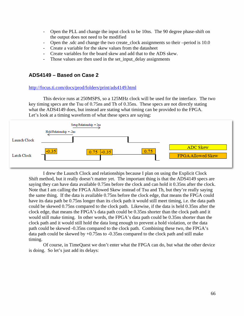
66
- Open the PLL and change the input clock to be 10ns. The 90 degree phase-shift on the output does not need to be modified
- Open the .sdc and change the two create_clock assignments so their –period is 10.0 - Create a variable for the skew values from the datasheet - Create variables for the board skew and add that to the ADS skew. - Those values are then used in the set_input_delay assignments
ADS4149 – Based on Case 2 http://focus.ti.com/docs/prod/folders/print/ads4149.html This device runs at 250MSPS, so a 125MHz clock will be used for the interface. The two key timing specs are the Tsu of 0.75ns and Th of 0.35ns. These specs are not directly stating what the ADS4149 does, but instead are stating what timing can be provided to the FPGA. Let’s look at a timing waveform of what these specs are saying:
I drew the Launch Clock and relationships because I plan on using the Explicit Clock Shift method, but it really doesn’t matter yet. The important thing is that the ADS4149 specs are saying they can have data available 0.75ns before the clock and can hold it 0.35ns after the clock. Note that I am calling the FPGA Allowed Skew instead of Tsu and Th, but they’re really saying the same thing. If the data is available 0.75ns before the clock edge, that means the FPGA could have its data path be 0.75ns longer than its clock path it would still meet timing, i.e. the data path could be skewed 0.75ns compared to the clock path. Likewise, if the data is held 0.35ns after the clock edge, that means the FPGA’s data path could be 0.35ns shorter than the clock path and it would still make timing. In other words, the FPGA’s data path could be 0.35ns shorter than the clock path and it would still hold the data long enough to prevent a hold violation, or the data path could be skewed -0.35ns compared to the clock path. Combining these two, the FPGA’s data path could be skewed by +0.75ns to -0.35ns compared to the clock path and still make timing. Of course, in TimeQuest we don’t enter what the FPGA can do, but what the other device is doing. So let’s just add its delays:

67
So we will be using Case 2, where the external device shifts the clock, sending it center-aligned. Once we have a 2ns setup relationship and -2ns hold relationship, the ADC’s delays will have a maximum of (2 – 0.75) = 1.25ns and a minimum of (-2 – (-0.35)) = -1.65ns. Making sure we understand the waveform, when the rising edge from the launch clock sends data, the ADC can skew the data by 1.25ns to -1.65ns compared to the clock, which leaves the FPGA with the ability to skew the data by 0.75ns to -0.35ns compared to the clock. After that, we will account for external board skew, which reduces the FPGA’s skew. To create the project:
- Copy project from Case 2. - The clock period is 8ns, which is correct, so no need to edit. - I moved the “–waveform {2.0 6.0}” option from the base clock to the external virtual
clock. This is discussed in detail in the options for Case 2. This step could be skipped and the analysis would be identical, it’s just a matter of personal preference.
- Calculated what the ADS4149 delays are based on the setup and hold relationship, as well as the Tsu/Th from the datasheet.
- Added board skew of +/-0.050ns to external delays. This value was randomly chosen.
- After compiling, the design made setup timing by 150ps but failed hold by -15ps. Looking at the Fitter Report -> Delay Chain Summary, the fitter had added 1 delay tap, with a delay of ~0.663ns, to help close timing. This certainly helped, as hold timing would have failed by hundreds of ps, but the delay chains are too coarse and it over-shot the setup margin.
- This device’s delays are not symmetric. We will account for that by adding a phase-shift of 200ps to the FPGA’s PLL. As discussed in “Exactly 90 °?”, this is perfectly fine. Note that we’re not changing what the external device looks like. In fact, we don’t need to change the .sdc at all, since the PLL is constrained by derive_pll_clocks. The reason we add 200ps is because the external device has a larger –max value than –min value, making it more difficult to meet setup timing and easier to meet hold. A positive phase-shift on the latch clock eases setup timing while making hold timing more difficult, i.e. countering the unbalanced external delays.
- The design now meets timing with 56 and 61ps of margin. Note that “balancing the requirements” does not always work. Sometimes a device’s path may be better off with a slight shift from center, which would need to be determined on a case by case basis. In this case, I balanced the requirements as a starting point and it worked.

68
Some users may be questioning the FPGA phase-shift we just did to this design. Specifically, we used the ADS4149’s Tsu and Th along with the setup and hold relationship to determine the external –max and –min values, then changed the setup and hold relationship due to a shift in the FPGA’s PLL, but did not change the external –max and –min values. The reason this is allowed is that the original setup and hold relationships were based solely on the clock coming into the FPGA, ssync_rx_fpga. If the FPGA phase-shifts that clock again doesn’t really matter as far as determining the ADS4149’s timing.
Note that we could have chosen a different phase for the external clock, and it would have worked out. For example, let’s say we chose to do this with the Implicit Clock Shift method, targeting the default next edge. In this case, neither the virtual clock nor the clock coming into the FPGA would use the –waveform {2.0 6.0} option, keeping them edge-aligned across the interface. The waveforms would look like so:
First off, the setup relationship becomes 4ns and the hold relationship becomes 0ns. I drew the setup from the rising edge and the hold from the falling edge because they overlap, but every rising and falling edge has both a setup and hold analysis. I then drew the Tsu and Th values in orange as before, with a 0.75ns allowed skew for setup analysis, and a -0.35ns allowed skew for hold analysis. The difference is that the different setup and hold relationships would have us compute different external delay values in yellow, with a –max of 3.25ns and –min of 0.35ns. This waveform shows that when the external clock launches data, for setup analysis, the ADS4149 might delay the data path by 3.25ns compared to the clock path, and hence the FPGA is allowed to delay the data path by 0.75ns compared to the clock path and still meet timing. Likewise for hold, the ADS4149 will delay the data path by a minimum of 0.35ns compared to the clock being sent, and so the FPGA is allowed to have its data path be 0.35ns shorter that the clock path and still meet timing. As expected, all this does is shift the setup and hold relationships by 2ns, going from +/-2ns to 4ns/0ns. To counter this shift, the external delays also end up being shifted, from 1.25ns/-1.65ns to 3.25ns/0.35ns. The final requirements on the FPGA are the same: Original Explicit Clock Shift Method:
Setup Analysis: FPGA_Data_Delay – FPGA_Clock_Delay < 2 – 1.25 Hold Analysis: FPGA_Data_Delay – FPGA_Clock_Delay > -2 – (-1.65) With Implicit Clock Shift: Setup Analysis: FPGA_Data_Delay – FPGA_Clock_Delay < 4 – 3.25

69
Hold Analysis: FPGA_Data_Delay – FPGA_Clock_Delay > 0 – (0.35) Both methods end up with the right side having 0.75ns for setup analysis and -0.35ns for
hold analysis. The reason this case is difficult is that the ADS4149 does not describe what it is doing, and instead specs what relationship it can transfer the data to the FPGA. This can be described in multiple ways.
This example also shows one of the things I dislike about the Implicit Clock Shift Method. With the Explicit Method, we used the PLL inside the FPGA to phase-shift the clock 200ps and get better timing margin. But with the Implicit Clock Shift Method, a 200ps phase-shift on the latch clock would create a default setup relationship of 0.2ns and default hold relationship of -3.8ns. To get the setup relationship of 2.2ns and hold of 0.2ns, we would need to add a multicycle like so:
set_multicycle_path –setup –from [get_clocks ssync_clk_ext] –to [get_clocks ssync_rx_clk] 2
This is discussed in the section “Exactly 90°?” The attached example uses the Explicit Clock Shift Method, since that avoids this, and in my opinion, makes more sense.
DAC5675a – Based on Case 3 http://focus.ti.com/docs/prod/folders/print/dac5675a.html We will run this DAC at the max rate of a 200MHz clock, for a 400Mbps data rate. The spec for this device is quite straightforward, a Tsu of 1.5ns and Th of 0.0ns. Remember that Tsu is the same thing as maximum data delay, in that the data path in the receiver could be up to 1.5ns longer than the clock path, and so the external device must have the data available 1.5ns before the clock. Likewise Th is the inverse of the minimum data delay, in that the data path could be up to 0ns shorter than the clock path, and so the external device must hold the data for that long. (It’s not apparent when Th is 0, but basically Th is inverted and used for the –min value in set_output_delay). Since a positive Tsu and Th mean the incoming clock edge can’t be at the same time as the data edge, we know the FPGA needs to phase-shift the clock, and hence we will use Case 3. Let’s look at a waveform with a 90° phase-shift on the clock being sent, with the external data delays, but not board skew for now:

70
This only shows the setup analysis from the rising edge of the launch clock and hold analysis from the falling edge, but both edges have an equivalent setup and hold relationship. Showing the max DAC delays of 1.5 and min delays of 0, the FPGA is allowed to skew its output data in relation to its output clock by -0.25 to -1.25ns. This is NOT center-aligned, and pretty far from it. Basically the DAC has non-symmetric delays for max and minimum, and so we need to re-center for that by phase-shifting the output clock another (1.5 + 0)/2 = 0.75ns. This is on top of the original 90° shift of 1.25ns, for a total of 2ns. The new waveform looks like so:
With a 2ns phase-shift on the output clock, the setup relationship becomes 2ns and the hold relationship becomes -0.5ns. For setup analysis, if the DAC can chew up 1.5ns of that 2ns relationship, then the FPGA can skew its output data by 0.5ns compared to the output clock and still meet timing. Likewise, the hold relationship is -0.5ns and 0ns of that is chewed up by the DAC, so the FPGA can skew its output data by -0.5ns compared to the output clock. In essence, the data can be +/-0.5ns compared to the output clock. Note that with the Explicit Clock Shift Method, using the PLL to shift the clocks around is perfectly acceptable and the user does not have to make any changes to the external delays. This is explained in the section called Exactly 90°? So the steps for creating this project were:
- Copy project from Case 3. - Open the PLL in Megawizard and change input clock to 200MHz and the phase-shift
on output clock c1 to be 2ns(it can’t do that exactly, and instead makes it 2.08ns) - Modify the .sdc so the incoming clock fpga_clk has a 5ns period - Modify the .sdc so the external devices max and min delays are 1.5ns and 0ns - Add in the board skew. I used +/-0.05ns as a place-holder. (This particular interface
barely meets timing, and so minimal board skew is imperative.) - Sum the DAC delays and board skew so they can be used in the output delay
assignment
DAC5681 – Based on Case 4 http://focus.ti.com/docs/prod/folders/print/dac5681.html
We will run this DAC with a 250MHz clock, resulting in a 500Mbps data rate between the FPGA and DAC. The important spec is tSkew, which is Dclk to Data and has values of +600ps and -1000ps when running at 250MHz. It’s not explicitly clear, but this spec is not

71
saying what the DAC does to the data, but is really saying how much skew the FPGA and board can put on the clock/data relationship. In other words, the FPGA is transmitting edge-aligned, with a skew of +600ps/-1000ps. For that, I copied the project from Case 4. I modified the PLL to have a 250MHz input, and I modified the create_clock in the .sdc so the fpga_clk is 4ns.
The create_generated_clock in the .sdc has the –phase 90 option, to specify that the DAC
is phase-shifting the clock 90 degrees, yet the data sheet never explicitly says it is doing that. Some users may have trouble with this, but another way of thinking of this is what it tells the FPGA. By saying the external device is shifting the clock into the middle of the data eye, we’re telling the FPGA to send out the clock and data edge-aligned, which is what we want.
Now let’s figure out what the external delays are. First off, it states the skew in terms of DCLK to Data. That is the opposite of how TimeQuest works, as we want to analyze the data path compared to the clock. So let’s reverse those numbers and say that the DAC’s allowed Data to Dclk skew is +1000ps/-600ps. Now things get a bit tricky, because the DAC datasheet says what is allowed externally to it. We need to reverse that to determine what the DAC is doing, and feed that into TimeQuest which will we determine what the FPGA can do. Describing this is difficult, so let’s look at a waveform:
I first drew the two waveforms with the 90° phase-shift that we have described.
The DAC datasheet says the FPGA can skew its data by +1000ps/-600ps relative to the its clock. So I drew those in yellow. If that’s what the DAC allows, then it uses the rest of the data window internally, so I drew those in orange. (Admittedly the 0ns –max delay of the DAC should be non-existent, but I made it just big enough to write 0 into it.)
Using equations, the DAC’s maximum data to clock skew is (setup_relationship – max_allowed_skew) = (90° - max_allowed_skew) = (1 – 1) = 0ns. That is the equation used in the .sdc. Likewise the DAC’s minimum data to clock skew is (hold_relationship – min_allowed_skew) = (-90° - min_allowed_skew) = (-1 – (-0.6)) = -0.4ns. The equations work, but I think the waveform helps conceptualize what’s going on. And though I would argue we’ve modeled what the DAC is actually doing, the most important thing is that our description tells the FPGA it can delay its data by +1ns to -0.6ns compared to the clock. Finally, I added in variables for the board skew, where a positive number states how much the data path is longer than DCLK, while a negative number states how much shorter it is. I randomly chose +/-0.1ns, but it would depend on the board layout. Notes:
- The data period is 2ns and the DAC allows a skew of +1ns to -0.6ns. That means the DAC is only skewing DCLK to Data by 0.4ns, which is a small number. This DAC

72
can run twice as fast though, where the data period is only 1ns, in which case the skew becomes sizable.
- It’s certainly confusing to have the DAC spec what it can handle, which we use to describe what the DAC is actually doing, which we tell TimeQuest so it can determine what the FPGA can do. If TimeQuest were instead used to spec what it could do, it would make this situation easier, but in cases where the external device specs what it is doing such as TI DAC 5675a, we would still have to work backwards to calculate the constraints. Since there is no universal methodology for making these constraints, there are always combinations that end up having the user work backwards. (There are other reasons why TimeQuest requires what the external device is doing; it’s not just a random choice.)
- It’s also annoying that we have to use the data period(or ninety degrees of the data period) in our calculations. Because of this, we can’t just change the base clock period and have everything auto-calculate. Once again, this is because the DAC doesn’t describe what it does but instead what it can handle. In fact, as the frequency chances, the DAC changes its allowed skew. In reality, the DAC should be adding the same amount of skew under all conditions, but as the data window widens and narrows, the allowed skew externally widens and narrows with it.
- The external delays are not symmetric, meaning the FPGA will have to vary the clock and data delays to get optimal slacks. It’s certainly possible that the user could do this with the PLL. Basically, the PLL would have two outputs, one that drives the clock and one that drives the data. They could either skew the clock driving data by +200ps or the clock driving DCLK by -200ps. It meets timing with plenty of slack as-is, but that is an option, as described in the section Exactly 90°?
- Since the DAC never explicitly says what it is doing, we could have described it in various ways. For example, we could have used Case 6, where the clocks are described as being edge-aligned across the interface. This would result in a 4ns setup relationship and 0ns hold relationship. We would have then calculated different external delays, where the max would be (4 – 1.0) = 3ns, and the min would have been (0 – (-0.6)) = 0.6ns. These external delays would have been then used to constrain the FPGA the same way. The FPGA’s setup relationship to the external device would be 4ns, the external delay would be 3ns, which means the FPGA can skew its data by 1ns compared to the clock and still meet timing. Likewise the hold relationship is -1ns and the
FPGA to FPGA Interfaces FPGA to FPGA interfaces are actually quite difficult to constrain, largely because both sides are so flexible it is hard to determine where to start. I will describe one solution that I would consider to probably be the best, but there are certainly other ways to approach this problem. First off, we will use the Explicit Clock Shift Method for both the transmitter and receiver. Second, we must decide who will shift the clock into the middle of the data window, the transmitter or the receiver. I think the best way to do this is to have the transmitter send data and clock edge-aligned and let the receiver phase-shift the clock into the middle of the data window. There two major reasons:

73
- If the transmitter shifts the clock, it must use an entire global clock tree just to get this newly shifted clock out. Sending data and clock edge-aligned can use the same clock tree for both. It also saves a PLL output tap, but that’s seldom an issue. Note that if the interface is SDR instead of DDR, then the clock could be shifted into the middle of the data eye by just inverting it, but for higher speeds most designs rely on DDR.
- For optimal performance at the receiver, a PLL is necessary to compensate for the large clock tree delays. As long as the PLL is being used, it might as well be the one to shift the clock 90° into the middle of the data window.
So with that decision, Case 4 will be used as the transmitter example and Case 1 will be used as the receiver. The /FPGA_to_FPGA directory started with a copy of those two projects. We will modify them for optimal performance across the link.
Probably the most difficult part of this problem is getting an initial timing constraint for either the transmitter or receiver, since we need to know what the other one is doing. Because of this, I recommend taking the following steps:
1) Over-constrain the transmitting FPGA so that it allows 0ns of skew. It will fail this requirement, but try to get the least amount of skew it can.
2) Loosen the constraints on the transmitter FPGA by however much it failed timing, so that it now barely meets timing.
3) Plug the transmitter’s skew and board skew into the receive FPGA’s .sdc. It will now try to meet timing based on the external skew.
4) Optional: If the receiving FPGA meets timing with lots of margin, the user can loosening the requirements on the transmitter FPGA, which will tighten the requirements on the receive FPGA, thereby spreading the slack between the two devices.
Let’s go through the example project to see how this is done. First open the project in /FPGA_to_FPGA/FPGATransmitter_BasedOn_Case_4. Opening the .sdc will show the following constraints:
set clk_period 8.0 set 90degrees [expr $clk_period / 4.0] set tx_output_skew_max 0.0 set tx_output_skew_min -0.0 set ext_skew_max [expr $90degrees - $tx_output_skew_max] set ext_skew_min [expr -$90degrees - $tx_output_skew_min] (Note: The tx_output_skew_max/min variables are actually set to +/-0.36 in the .sdc, while the step to setting them to 0 is commented out. If the user wants to follow through each step, they should comment out the current constraint and uncomment the one that sets them to 0. The .sdc is currently showing the “final values”.) The first two lines just calculates 90° of the clock period, which in this case is 2ns. Since we’re using the Explicit Clock Shift Method, we know the setup relationship is 90° and the hold relationship is -90°. The next two lines say how much skew we’re going to allow on the output, which I’ve set to 0. The last two lines calculate the external skew. Basically to describe what the transmitter can do, we must say the external device chews up the rest of the relationship. So

74
in this example, if the setup relationship is 2ns, and we calculate the external device has a max delay of 2ns, the transmitter needs to have +0ns of skew on its output. Likewise if the hold relationship is -2ns, and the external device’s min delay is -2ns, then the transmitter can have -0ns of skew on its output. (I use +0 and -0 to differentiate between max analysis and min analysis, but obviously they’re the same thing). As expected, the interface fails timing after compiling, since it is impossible to have +/-0ns of skew. Running the TQ_analysis.tcl in TimeQuest, I see that the interface fails setup timing by -355ps and hold timing by -352ps, which means the data may be skewed from the clock by coming out 355ps after the clock to 352ps before the clock. Rounding up to 360ps, I then change the transmit skew to the following: set tx_output_skew_max 0.360 set tx_output_skew_min -0.360 Just re-running TimeQuest shows that this meets timing. There is no need to place-and-route again, but I did do that and it met timing by 5ps and 8ps, as expected. (Note that I locked the pins down, as letting them float added some variation from compile to compile that wouldn’t exist in a real design). Now it’s time to constrain the receive side. This is quite straightforward, since we know the details of everything external. The constraints are: set tx_output_skew_max 0.360 set tx_output_skew_min -0.360 set brd_skew_max 0.1 set brd_skew_min -0.1 set ssync_input_delay_max [expr $tx_output_skew_max + $brd_skew_max] set ssync_input_delay_min [expr $tx_output_skew_min + $brd_skew_min] The first two numbers are directly out of the transmit FPGA’s .sdc. Since that FPGA is constrained to have a skew of +/-360ps, I just took those numbers directly. I then added two values for board skew(positive is how much longer the data is than the clock, negative is how much shorter). The final step is just to add them together. This example results in an external max delay of 0.37ns and min delay of -0.37ns. Technically we’re done, assuming both sides meet timing. One thing to note though is that the receiver met timing with a setup slack of 886ps and a hold slack of 1.182ns. So the transmitter is only meeting timing by a few picoseconds, while the receiver has hundreds of picoseconds. The user can optionally share that slack between the two devices. In my case, I would take 400ps of slack and move it to the transmitter. This is done by changing the transmitter output skew by 400ps to: set tx_output_skew_max 0.760 set tx_output_skew_min -0.760

75
Note that this must be done in BOTH .sdc files. I added this to the .sdc files, but left it commented out. The user can put in any value for the allowed skew on the transmitter, and by copying that value into the receive FPGA’s .sdc, will properly constrain the receiver. Another way I have seen user’s attack this problem is to try and give a percentage of the transfer to each side. For example, the setup relationship is 2ns, and they might try to give 50% to the transmitter and 50% to the receiver. This gets tricky if there is any board skew, as that must be taken out first. So if the max board skew is 0.1ns(data is longer than clock by 0.1ns), then the allowed skew for each side would be (2 – 0.1)/2 = 0.95ns. Since they’ve determined the allowed skew, they would then need to calculate what the external device is doing, which is (2 – 0.95) = 1.05ns. I’ve done this before, and found the whole method to be difficult to follow, and why I recommend the approach taken above, whereby the transmitter is constrained first to have the minimal amount of skew it can achieve, and then the receiver is constrained in relation to what the transmitter achieved.