sound processors for boom box / mini-component stereo...
TRANSCRIPT
1/18 www.rohm.com 2010.10 - Rev.A
© 2010 ROHM Co., Ltd. All rights reserved.
Sound Processors for BOOM BOX / Mini-component Stereo
Single Power Supply Sound Processors with Built-in Pre Amplifier for Tape Recording and Play Back (With Integrated 2-/3- band Equalizer) BD3401KS2,BD3402KS2
Description
The Sound Processor with built-in record/play functions for cassette players, is suited for sound quality products such as, BOOM BOX, mini- and micro-audio systems. It incorporates various functions ranging from audio source selectors to preamplifiers at the front stage, preamplifier for cassette recording/playing, and a 2-wire serial bus.
Features 1) Provides Surround and Bass Boost with the Soft-switching feature to reduce the shock sound at switching (BD3401KS2) 2) Provides a specialized power supply terminal in a digital circuit, in order to set and maintain the state inside the IC by the minute stand-by current. 3) Built-in preamplifier for cassette recording/playing allows for minimal external components, freeing up board space. 4) Arranges all I/O terminals to a single point and allows easy PCB routing. 5) Volume and Tone implemented with a resistance ladder circuit; achieving high performance with low noise and low distortion 6) Energy-saving design resulting in low current consumption, by utilizing the BiCMOS process. It has the advantage in quality over the scaling down the power heat control of the internal regulators.
Applications
BOOM BOX, mini-audio systems, and micro-audio systems. Product lineup
Parameter BD3401KS2 BD3402KS2
Equalizer 3 band(BASS, MIDDLE, TREBLE) 2 band(BASS, TREBLE)
Volume 0 to -44dB/2dB step
-44 to -76dB/4dB step, -∞dB 0 to -44dB/2dB step
-44 to -76dB/4dB step, -∞dB
Cassette Recording/Playing Amplifier
Karaoke -
Microphone Input -
Subwoofer Output -
Output for Spectrum Analyzer -
Surround -
Bass Boost -
Package SQFP-T64 SQFP-T64 Absolute maximum ratings (Ta=25)
Items Symbol Ratings Unit
Power Supply Voltage Vcc 10 V
Vdd 6 V
Power Dissipation Pd 1200* mW
Input Voltage Range Vin GND-0.3 to VCC+0.3 V
Operating Temperature Range Topr -25 to +75
Storage Temperature Range Tstg -55 to +125 * Reduced by 12 mW/ over 25, when installed on the standard board (size: 70×70×1.6mm).
Operating voltage range
Device Name Symbol Range Unit
BD3401KS2 BD3402KS2
Vcc 8 to 9.5 V
Vdd 3 to 5.5
No.10086EAT03
Technical Note
2/18 www.rohm.com 2010.10 - Rev.A
© 2010 ROHM Co., Ltd. All rights reserved.
BD3401KS2,BD3402KS2
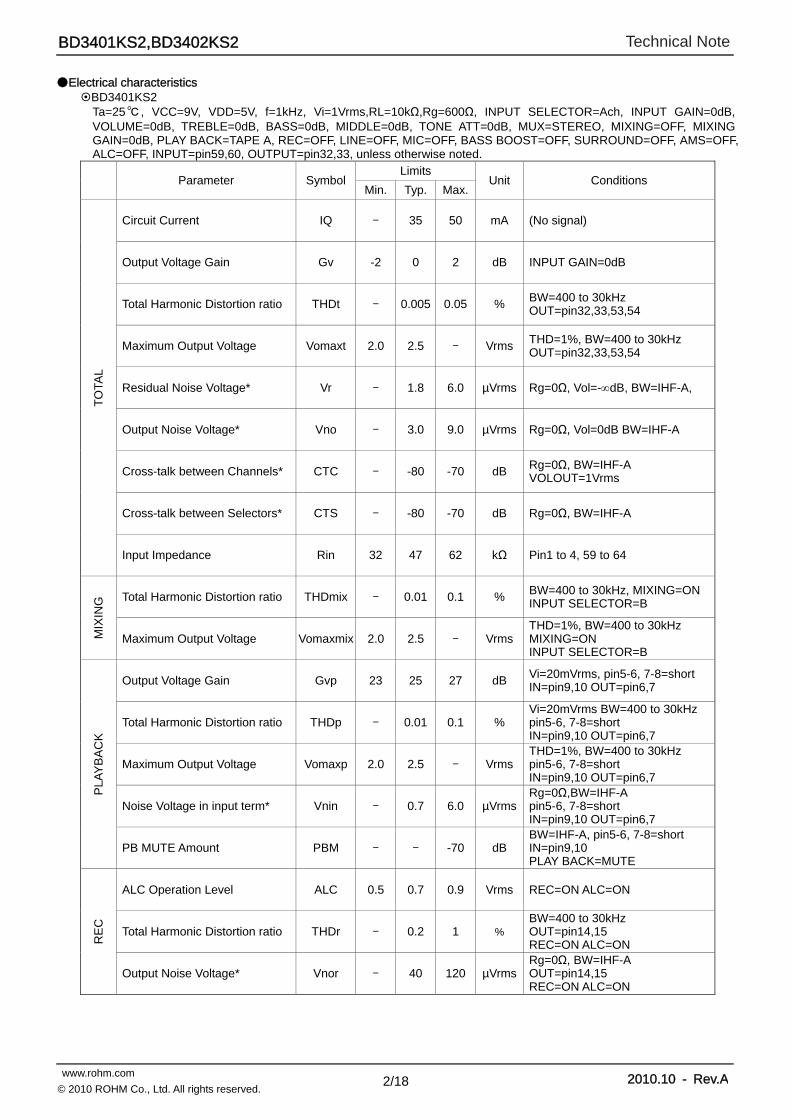
Electrical characteristics BD3401KS2
Ta=25 , VCC=9V, VDD=5V, f=1kHz, Vi=1Vrms,RL=10kΩ,Rg=600Ω, INPUT SELECTOR=Ach, INPUT GAIN=0dB, VOLUME=0dB, TREBLE=0dB, BASS=0dB, MIDDLE=0dB, TONE ATT=0dB, MUX=STEREO, MIXING=OFF, MIXING GAIN=0dB, PLAY BACK=TAPE A, REC=OFF, LINE=OFF, MIC=OFF, BASS BOOST=OFF, SURROUND=OFF, AMS=OFF, ALC=OFF, INPUT=pin59,60, OUTPUT=pin32,33, unless otherwise noted.
Parameter SymbolLimits
Unit Conditions Min. Typ. Max.
TO
TAL
Circuit Current IQ - 35 50 mA (No signal)
Output Voltage Gain Gv -2 0 2 dB INPUT GAIN=0dB
Total Harmonic Distortion ratio THDt - 0.005 0.05 % BW=400 to 30kHz OUT=pin32,33,53,54
Maximum Output Voltage Vomaxt 2.0 2.5 - Vrms THD=1%, BW=400 to 30kHz OUT=pin32,33,53,54
Residual Noise Voltage* Vr - 1.8 6.0 µVrms Rg=0Ω, Vol=-dB, BW=IHF-A,
Output Noise Voltage* Vno - 3.0 9.0 µVrms Rg=0Ω, Vol=0dB BW=IHF-A
Cross-talk between Channels* CTC - -80 -70 dB Rg=0Ω, BW=IHF-A VOLOUT=1Vrms
Cross-talk between Selectors* CTS - -80 -70 dB Rg=0Ω, BW=IHF-A
Input Impedance Rin 32 47 62 kΩ Pin1 to 4, 59 to 64
MIX
ING
Total Harmonic Distortion ratio THDmix - 0.01 0.1 % BW=400 to 30kHz, MIXING=ON INPUT SELECTOR=B
Maximum Output Voltage Vomaxmix 2.0 2.5 - VrmsTHD=1%, BW=400 to 30kHz MIXING=ON INPUT SELECTOR=B
PLA
YB
AC
K
Output Voltage Gain Gvp 23 25 27 dB Vi=20mVrms, pin5-6, 7-8=short IN=pin9,10 OUT=pin6,7
Total Harmonic Distortion ratio THDp - 0.01 0.1 % Vi=20mVrms BW=400 to 30kHz pin5-6, 7-8=short IN=pin9,10 OUT=pin6,7
Maximum Output Voltage Vomaxp 2.0 2.5 - VrmsTHD=1%, BW=400 to 30kHz pin5-6, 7-8=short IN=pin9,10 OUT=pin6,7
Noise Voltage in input term* Vnin - 0.7 6.0 µVrmsRg=0Ω,BW=IHF-A pin5-6, 7-8=short IN=pin9,10 OUT=pin6,7
PB MUTE Amount PBM - - -70 dB BW=IHF-A, pin5-6, 7-8=short IN=pin9,10 PLAY BACK=MUTE
RE
C
ALC Operation Level ALC 0.5 0.7 0.9 Vrms REC=ON ALC=ON
Total Harmonic Distortion ratio THDr - 0.2 1 % BW=400 to 30kHz OUT=pin14,15 REC=ON ALC=ON
Output Noise Voltage* Vnor - 40 120 µVrmsRg=0Ω, BW=IHF-A OUT=pin14,15 REC=ON ALC=ON
Technical Note
3/18 www.rohm.com 2010.10 - Rev.A
© 2010 ROHM Co., Ltd. All rights reserved.
BD3401KS2,BD3402KS2
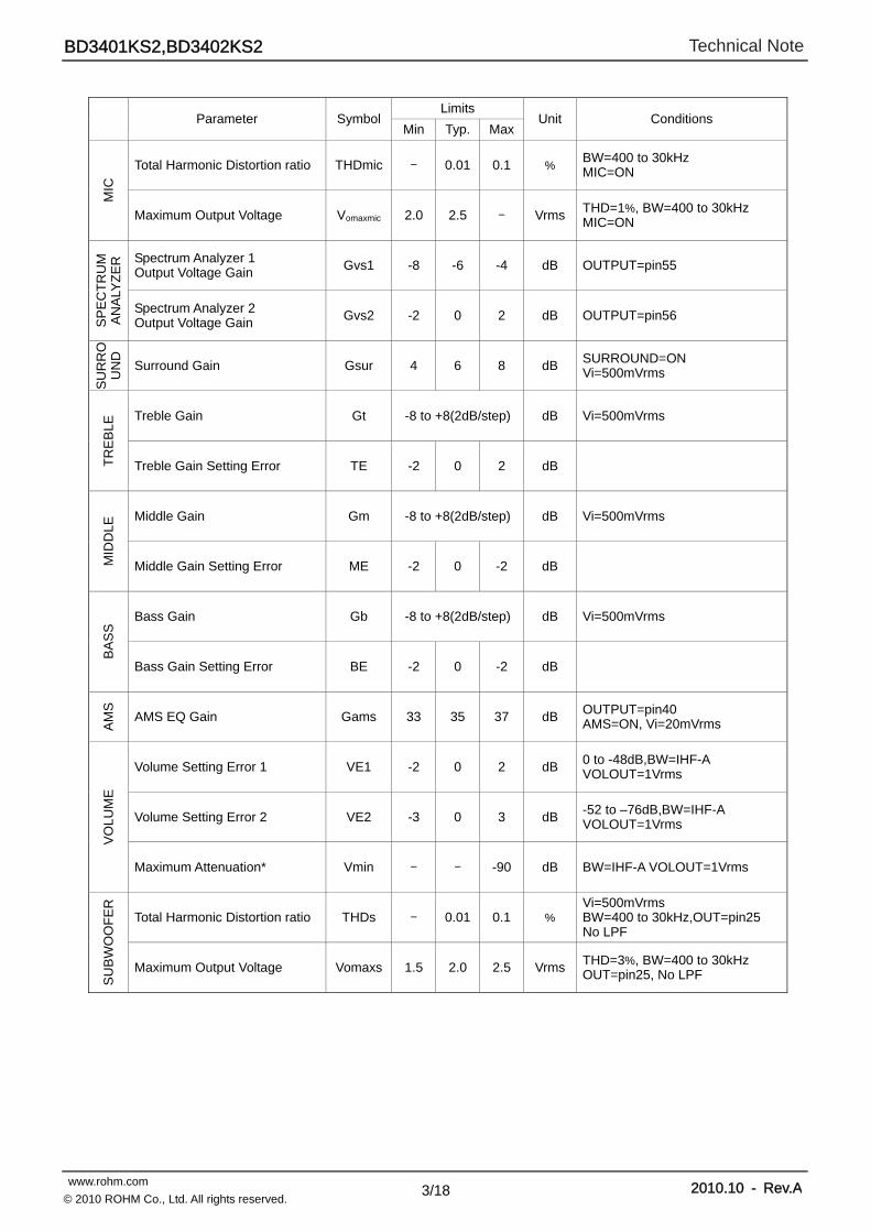
Parameter SymbolLimits
Unit Conditions Min Typ. Max
MIC
Total Harmonic Distortion ratio THDmic - 0.01 0.1 % BW=400 to 30kHz MIC=ON
Maximum Output Voltage Vomaxmic 2.0 2.5 - VrmsTHD=1%, BW=400 to 30kHz MIC=ON
SP
EC
TR
UM
A
NA
LYZ
ER
Spectrum Analyzer 1 Output Voltage Gain
Gvs1 -8 -6 -4 dB OUTPUT=pin55
Spectrum Analyzer 2 Output Voltage Gain
Gvs2 -2 0 2 dB OUTPUT=pin56
SU
RR
OU
ND
Surround Gain Gsur 4 6 8 dB SURROUND=ON Vi=500mVrms
TR
EB
LE Treble Gain Gt -8 to +8(2dB/step) dB Vi=500mVrms
Treble Gain Setting Error TE -2 0 2 dB
MID
DLE
Middle Gain Gm -8 to +8(2dB/step) dB Vi=500mVrms
Middle Gain Setting Error ME -2 0 -2 dB
BA
SS
Bass Gain Gb -8 to +8(2dB/step) dB Vi=500mVrms
Bass Gain Setting Error BE -2 0 -2 dB
AM
S
AMS EQ Gain Gams 33 35 37 dB OUTPUT=pin40 AMS=ON, Vi=20mVrms
VO
LUM
E
Volume Setting Error 1 VE1 -2 0 2 dB 0 to -48dB,BW=IHF-A VOLOUT=1Vrms
Volume Setting Error 2 VE2 -3 0 3 dB -52 to –76dB,BW=IHF-A VOLOUT=1Vrms
Maximum Attenuation* Vmin - - -90 dB BW=IHF-A VOLOUT=1Vrms
SU
BW
OO
FE
R
Total Harmonic Distortion ratio THDs - 0.01 0.1 % Vi=500mVrms BW=400 to 30kHz,OUT=pin25 No LPF
Maximum Output Voltage Vomaxs 1.5 2.0 2.5 Vrms THD=3%, BW=400 to 30kHz OUT=pin25, No LPF
Technical Note
4/18 www.rohm.com 2010.10 - Rev.A
© 2010 ROHM Co., Ltd. All rights reserved.
BD3401KS2,BD3402KS2
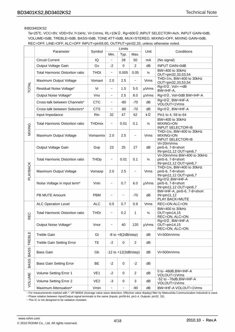
BD3402KS2
Ta=25, VCC=9V, VDD=5V, f=1kHz, Vi=1Vrms, RL=10kΩ, Rg=600Ω,INPUT SELECTOR=Ach, INPUT GAIN=0dB,
VOLUME=0dB, TREBLE=0dB, BASS=0dB, TONE ATT=0dB, MUX=STEREO, MIXING=OFF, MIXING GAIN=0dB,
REC=OFF, LINE=OFF, ALC=OFF INPUT=pin59,60, OUTPUT=pin32,33, unless otherwise noted.
Parameter SymbolLimits
Unit Conditions Min. Typ. Max.
TO
TAL
Circuit Current IQ - 28 50 mA (No signal)
Output Voltage Gain Gv -2 0 2 dB INPUT GAIN=0dB
Total Harmonic Distortion ratio THDt - 0.005 0.05 % BW=400 to 30kHz OUT=pin32,33,53,54
Maximum Output Voltage Vomaxt 2.0 2.5 - Vrms THD=1%, BW=400 to 30kHzOUT=pin32,33,53,54
Residual Noise Voltage* Vr - 1.5 5.0 µVrmsRg=0Ω, Vol=-∞dB BW=IHF-A,
Output Noise Voltage* Vno - 2.5 8.0 µVrms Rg=0Ω, Vol=0dB BW=IHF-A
Cross-talk between Channels* CTC - -80 -70 dB Rg=0Ω, BW=IHF-A VOLOUT=1Vrms
Cross-talk between Selectors* CTS - -80 -70 dB Rg=0Ω, BW=IHF-A
Input Impedance Rin 32 47 62 kΩ Pin1 to 4, 59 to 64
MIX
ING
Total Harmonic Distortion ratio THDmix - 0.01 0.1 % BW=400 to 30kHz MIXING=ON INPUT SELECTOR=B
Maximum Output Voltage Vomaxmix 2.0 2.5 - VrmsTHD=1%, BW=400 to 30kHzMIXING=ON INPUT SELECTOR=B
PLA
YB
AC
K
Output Voltage Gain Gvp 23 25 27 dB Vi=20mVrms pin5-6, 7-8=short IN=pin11,12 OUT=pin6,7
Total Harmonic Distortion ratio THDp - 0.01 0.1 % Vi=20mVrms BW=400 to 30kHzpin5-6, 7-8=short IN=pin11,12 OUT=pin6,7
Maximum Output Voltage Vomaxp 2.0 2.5 - VrmsTHD=1%, BW=400 to 30kHzpin5-6, 7-8=short IN=pin11,12 OUT=pin6,7
Noise Voltage in input term* Vnin - 0.7 6.0 µVrmsRg=0Ω,BW=IHF-A pin5-6, 7-8=short IN=pin11,12 OUT=pin6,7
PB MUTE Amount PBM - - -70 dB BW=IHF-A, pin5-6, 7-8=shortIN=pin11,12 PLAY BACK=MUTE
RE
C
ALC Operation Level ALC 0.5 0.7 0.9 Vrms REC=ON ALC=ON
Total Harmonic Distortion ratio THDr - 0.2 1 % BW=400 to 30kHz OUT=pin14,15 REC=ON, ALC=ON
Output Noise Voltage* Vnor - 40 120 µVrmsRg=0Ω, BW=IHF-A OUT=pin14,15 REC=ON, ALC=ON
TR
EB
LE
Treble Gain Gt -8 to +8(2dB/step) dB Vi=500mVrms
Treble Gain Setting Error TE -2 0 2 dB
BA
SS
Bass Gain Gb -12 to +12(3dB/step) dB Vi=500mVrms
BA
SS
Bass Gain Setting Error BE -2 0 -2 dB
VO
LUM
E Volume Setting Error 1 VE1 -2 0 2 dB 0 to -48dB,BW=IHF-A
VOLOUT=1Vrms
Volume Setting Error 2 VE2 -3 0 3 dB -52 to –76dB,BW=IHF-A VOLOUT=1Vrms
Maximum Attenuation* Vmin - - -90 dB BW=IHF-A VOLOUT=1Vrms ・For measurements marked with *, VP-9690A (Average value wave detection, Effective value display) filter by Matsushita Communication Industrial is used. ・Phase relation between Input/Output signal terminals is the same (Inputs: pin59-64, pin1-4, Outputs: pin32, 33). ・This IC is not designed to be radiation-resistant.
Technical Note
5/18 www.rohm.com 2010.10 - Rev.A
© 2010 ROHM Co., Ltd. All rights reserved.
BD3401KS2,BD3402KS2
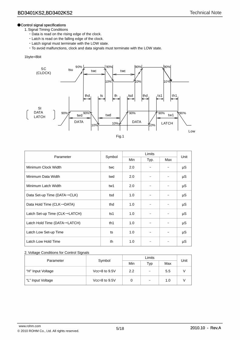
Control signal specifications 1. Signal Timing Conditions ・Data is read on the rising edge of the clock. ・Latch is read on the falling edge of the clock. ・Latch signal must terminate with the LOW state. ・To avoid malfunctions, clock and data signals must terminate with the LOW state.
1byte=8bit
Fig.1
Parameter Symbol Limits
Unit Min Typ. Max
Minimum Clock Width twc 2.0 - - µS
Minimum Data Width twd 2.0 - - µS
Minimum Latch Width tw1 2.0 - - µS
Data Set-up Time (DATA→CLK) tsd 1.0 - - µS
Data Hold Time (CLK→DATA) thd 1.0 - - µS
Latch Set-up Time (CLK→LATCH) ts1 1.0 - - µS
Latch Hold Time (DATA→LATCH) th1 1.0 - - µS
Latch Low Set-up Time ts 1.0 - - µS
Latch Low Hold Time th 1.0 - - µS
2. Voltage Conditions for Control Signals
Parameter Symbol Limits
Unit Min Typ Max
“H” Input Voltage Vcc=8 to 9.5V 2.2 - 5.5 V
“L” Input Voltage Vcc=8 to 9.5V 0 - 1.0 V
SC
(CLOCK)
SI DATA LATCH
thd thdth ts ts1 th1 tsd
twc
twd twd tw1
tsu
DATA DATA LATCH
90% 90% 90% 90%
10% 10% 10%
90% 90% 90% 90% 90%
10% 10% 10%
twc
Low
Technical Note
6/18 www.rohm.com 2010.10 - Rev.A
© 2010 ROHM Co., Ltd. All rights reserved.
BD3401KS2,BD3402KS2
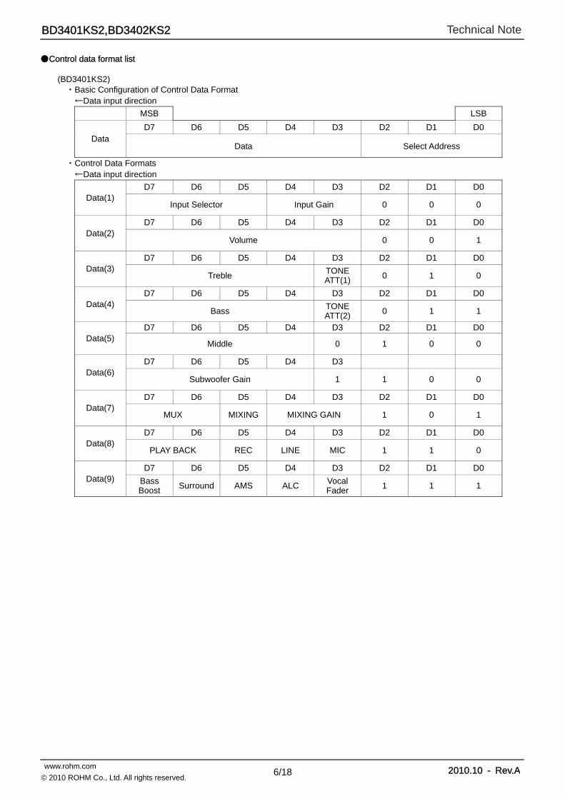
Control data format list
(BD3401KS2) ・Basic Configuration of Control Data Format ←Data input direction
MSB LSB
Data D7 D6 D5 D4 D3 D2 D1 D0
Data Select Address
・Control Data Formats ←Data input direction
Data(1) D7 D6 D5 D4 D3 D2 D1 D0
Input Selector Input Gain 0 0 0
Data(2) D7 D6 D5 D4 D3 D2 D1 D0
Volume 0 0 1
Data(3) D7 D6 D5 D4 D3 D2 D1 D0
Treble TONE ATT(1) 0 1 0
Data(4) D7 D6 D5 D4 D3 D2 D1 D0
Bass TONE ATT(2) 0 1 1
Data(5) D7 D6 D5 D4 D3 D2 D1 D0
Middle 0 1 0 0
Data(6) D7 D6 D5 D4 D3
Subwoofer Gain 1 1 0 0
Data(7) D7 D6 D5 D4 D3 D2 D1 D0
MUX MIXING MIXING GAIN 1 0 1
Data(8) D7 D6 D5 D4 D3 D2 D1 D0
PLAY BACK REC LINE MIC 1 1 0
Data(9) D7 D6 D5 D4 D3 D2 D1 D0
Bass Boost
Surround AMS ALC Vocal Fader
1 1 1
Technical Note
7/18 www.rohm.com 2010.10 - Rev.A
© 2010 ROHM Co., Ltd. All rights reserved.
BD3401KS2,BD3402KS2
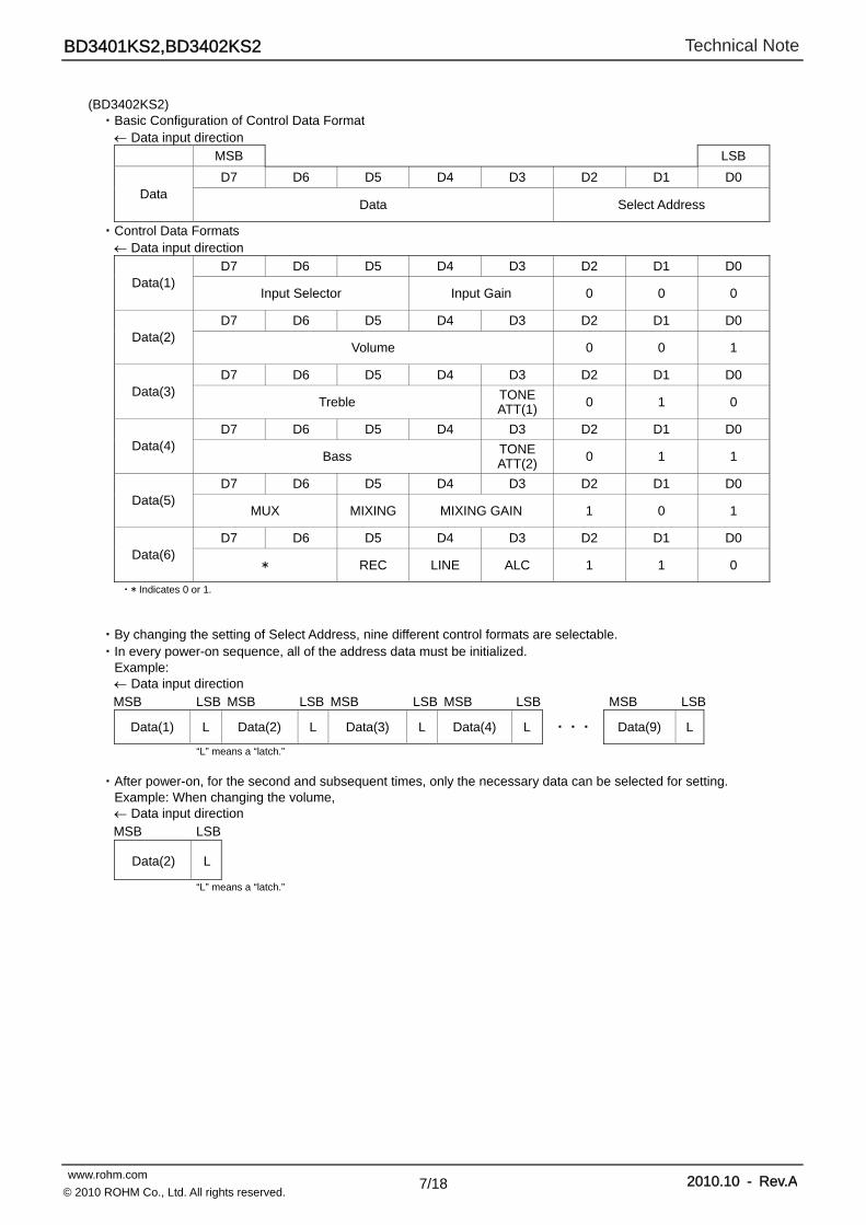
(BD3402KS2) ・Basic Configuration of Control Data Format Data input direction
MSB LSB
Data D7 D6 D5 D4 D3 D2 D1 D0
Data Select Address
・Control Data Formats Data input direction
Data(1) D7 D6 D5 D4 D3 D2 D1 D0
Input Selector Input Gain 0 0 0
Data(2) D7 D6 D5 D4 D3 D2 D1 D0
Volume 0 0 1
Data(3) D7 D6 D5 D4 D3 D2 D1 D0
Treble TONE ATT(1) 0 1 0
Data(4) D7 D6 D5 D4 D3 D2 D1 D0
Bass TONE ATT(2)
0 1 1
Data(5) D7 D6 D5 D4 D3 D2 D1 D0
MUX MIXING MIXING GAIN 1 0 1
Data(6) D7 D6 D5 D4 D3 D2 D1 D0
* REC LINE ALC 1 1 0
・* Indicates 0 or 1.
・By changing the setting of Select Address, nine different control formats are selectable. ・In every power-on sequence, all of the address data must be initialized.
Example: Data input direction MSB LSB MSB LSB MSB LSB MSB LSB MSB LSB
Data(1) L Data(2) L Data(3) L Data(4) L ・・・ Data(9) L
“L” means a “latch.”
・After power-on, for the second and subsequent times, only the necessary data can be selected for setting.
Example: When changing the volume, Data input direction MSB LSB
Data(2) L
“L” means a “latch.”
Technical Note
8/18 www.rohm.com 2010.10 - Rev.A
© 2010 ROHM Co., Ltd. All rights reserved.
BD3401KS2,BD3402KS2
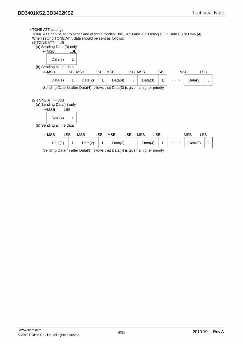
・TONE ATT settings
TONE ATT can be set to either one of three modes: 0dB, -4dB and -8dB using D3 in Data (3) or Data (4). When setting TONE ATT, data should be sent as follows: (1)TONE ATT=-4dB
(a) Sending Data (3) only MSB LSB
Data(3) L
(b) Sending all the data MSB LSB MSB LSB MSB LSB MSB LSB MSB LSB
Data(1) L Data(2) L Data(4) L Data(3) L ・・・ Data(9) L
Sending Data(3) after Data(4) follows that Data(3) is given a higher priority.
(2)TONE ATT=-8dB (a) Sending Data(4) only
←MSB LSB
Data(4) L
(b) Sending all the data
MSB LSB MSB LSB MSB LSB MSB LSB MSB LSB
Data(1) L Data(2) L Data(3) L Data(4) L ・・・ Data(9) L
Sending Data(4) after Data(3) follows that Data(4) is given a higher priority.
Technical Note
9/18 www.rohm.com 2010.10 - Rev.A
© 2010 ROHM Co., Ltd. All rights reserved.
BD3401KS2,BD3402KS2
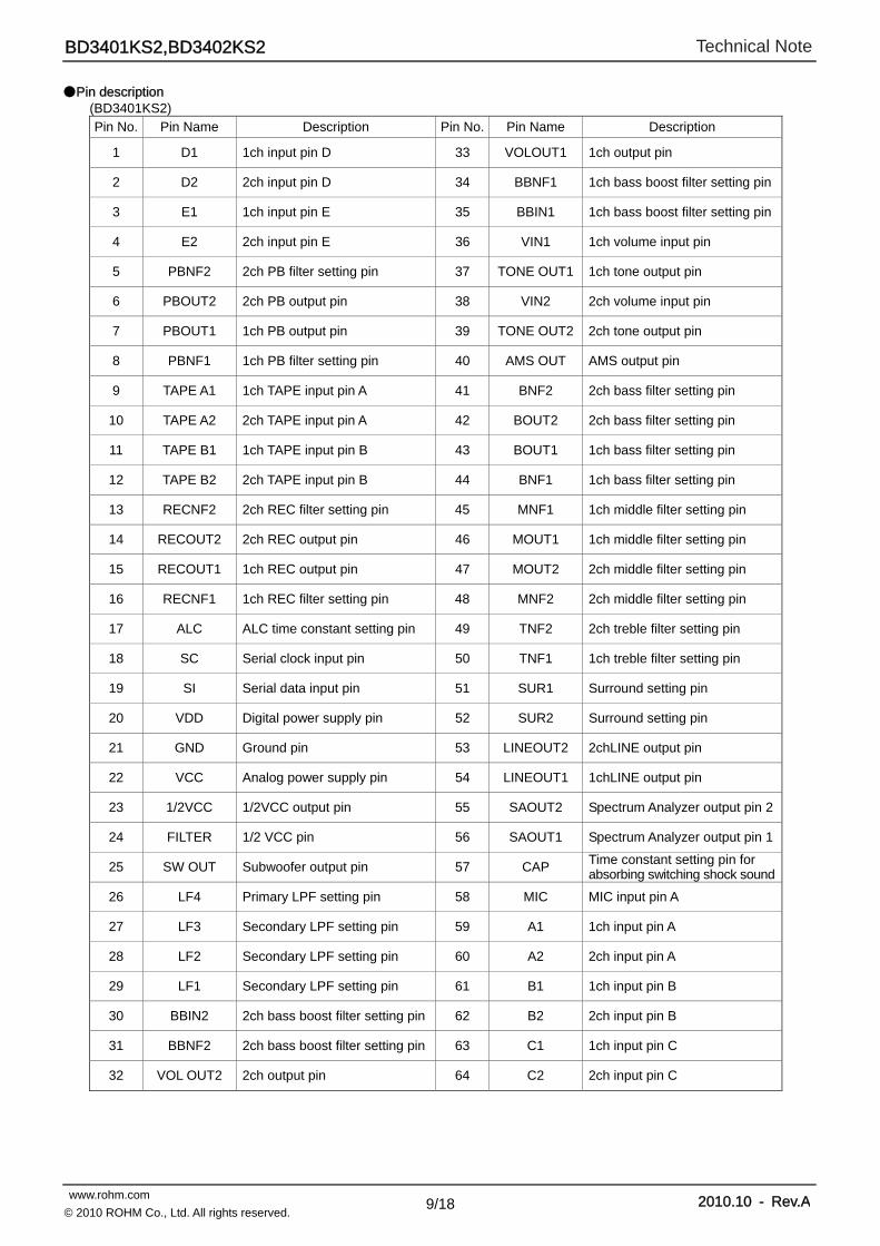
Pin description (BD3401KS2) Pin No. Pin Name Description Pin No. Pin Name Description
1 D1 1ch input pin D 33 VOLOUT1 1ch output pin
2 D2 2ch input pin D 34 BBNF1 1ch bass boost filter setting pin
3 E1 1ch input pin E 35 BBIN1 1ch bass boost filter setting pin
4 E2 2ch input pin E 36 VIN1 1ch volume input pin
5 PBNF2 2ch PB filter setting pin 37 TONE OUT1 1ch tone output pin
6 PBOUT2 2ch PB output pin 38 VIN2 2ch volume input pin
7 PBOUT1 1ch PB output pin 39 TONE OUT2 2ch tone output pin
8 PBNF1 1ch PB filter setting pin 40 AMS OUT AMS output pin
9 TAPE A1 1ch TAPE input pin A 41 BNF2 2ch bass filter setting pin
10 TAPE A2 2ch TAPE input pin A 42 BOUT2 2ch bass filter setting pin
11 TAPE B1 1ch TAPE input pin B 43 BOUT1 1ch bass filter setting pin
12 TAPE B2 2ch TAPE input pin B 44 BNF1 1ch bass filter setting pin
13 RECNF2 2ch REC filter setting pin 45 MNF1 1ch middle filter setting pin
14 RECOUT2 2ch REC output pin 46 MOUT1 1ch middle filter setting pin
15 RECOUT1 1ch REC output pin 47 MOUT2 2ch middle filter setting pin
16 RECNF1 1ch REC filter setting pin 48 MNF2 2ch middle filter setting pin
17 ALC ALC time constant setting pin 49 TNF2 2ch treble filter setting pin
18 SC Serial clock input pin 50 TNF1 1ch treble filter setting pin
19 SI Serial data input pin 51 SUR1 Surround setting pin
20 VDD Digital power supply pin 52 SUR2 Surround setting pin
21 GND Ground pin 53 LINEOUT2 2chLINE output pin
22 VCC Analog power supply pin 54 LINEOUT1 1chLINE output pin
23 1/2VCC 1/2VCC output pin 55 SAOUT2 Spectrum Analyzer output pin 2
24 FILTER 1/2 VCC pin 56 SAOUT1 Spectrum Analyzer output pin 1
25 SW OUT Subwoofer output pin 57 CAP Time constant setting pin for absorbing switching shock sound
26 LF4 Primary LPF setting pin 58 MIC MIC input pin A
27 LF3 Secondary LPF setting pin 59 A1 1ch input pin A
28 LF2 Secondary LPF setting pin 60 A2 2ch input pin A
29 LF1 Secondary LPF setting pin 61 B1 1ch input pin B
30 BBIN2 2ch bass boost filter setting pin 62 B2 2ch input pin B
31 BBNF2 2ch bass boost filter setting pin 63 C1 1ch input pin C
32 VOL OUT2 2ch output pin 64 C2 2ch input pin C
Technical Note
10/18 www.rohm.com 2010.10 - Rev.A
© 2010 ROHM Co., Ltd. All rights reserved.
BD3401KS2,BD3402KS2
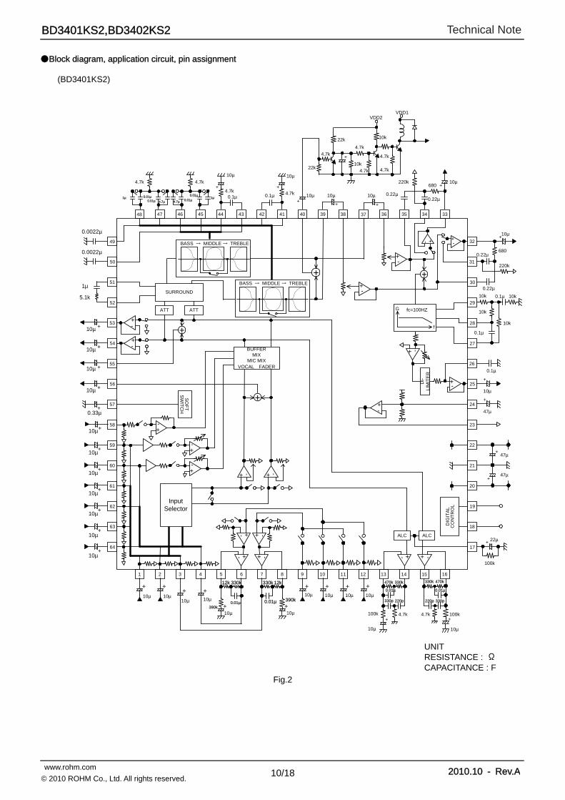
Block diagram, application circuit, pin assignment
(BD3401KS2)
Fig.2
UNIT RESISTANCE : Ω CAPACITANCE : F
1 2 3 4 5 6 7 8 9 10 11 12 13 14
64
63
62
61
60
59
58
57
56
55
54
53
52
51
46 45 44 43 42 41 40 39 38 37 36 35 34 33
17
18
19
20
21
22
23
24
25
26
27
28
29
30
15 16
48 47
50
49
31
32
+
DIG
ITA
LC
ON
TR
OL
Di-
LIM
ITE
R
+
SURROUND
ATT ATT
+-
+-+-
+ -+ -
+ - + -
+- + -
+-
+
+-
+ -
0
G fc=100HZ
f
ALC ALC
+-
+-
InputSelector
BUFFERMIX
MIC MIXVOCAL FADER
SO
FT
SW
ITC
H
+-
+-
+
+-
+-
+-
+-
BASS → MIDDLE → TREBLE
BASS → MIDDLE → TREBLE
+ +
+
+
+
+
+
+
+
+
++++
++
++
++
+
+
+
+
+
+
+
+
+
+
+
+
0.0022µ
0.0022µ
1µ
5.1k
10µ
10µ
10µ
10µ
0.33µ
10µ
10µ
10µ
10µ
10µ
10µ
10µ
10µ 10µ10µ 10µ
10µ390k
12k 330k 12k330k
0.01µ 0.01µ 390k
10µ
10µ 10µ 10µ 10µ
10µ
100k
+
4.7k
330p 220p
0.01µ
470k 330k
+
330k 470k
0.01µ
220p 330p
4.7k 100k
10µ
100k
47µ
22µ
47µ
47µ
10µ
0.1µ
0.1µ
10k
10k
10k 10k0.1µ
0.22µ
220k
0.22µ
10µ
680
10µ680
0.22µ
220k
0.22µ
+ +
10µ10µ10µ
10µ
4.7k0.1µ0.1µ4.7k
10µ
4.7k
1µ0.01µ
0.01µ 4.7µ4.7µ
0.01µ0.01µ
4.7k
1µ
+
22k
22k 4.7k
4.7k
4.7k
4.7k
10k
10k
VDD2VDD1
4.7k
Technical Note
11/18 www.rohm.com 2010.10 - Rev.A
© 2010 ROHM Co., Ltd. All rights reserved.
BD3401KS2,BD3402KS2
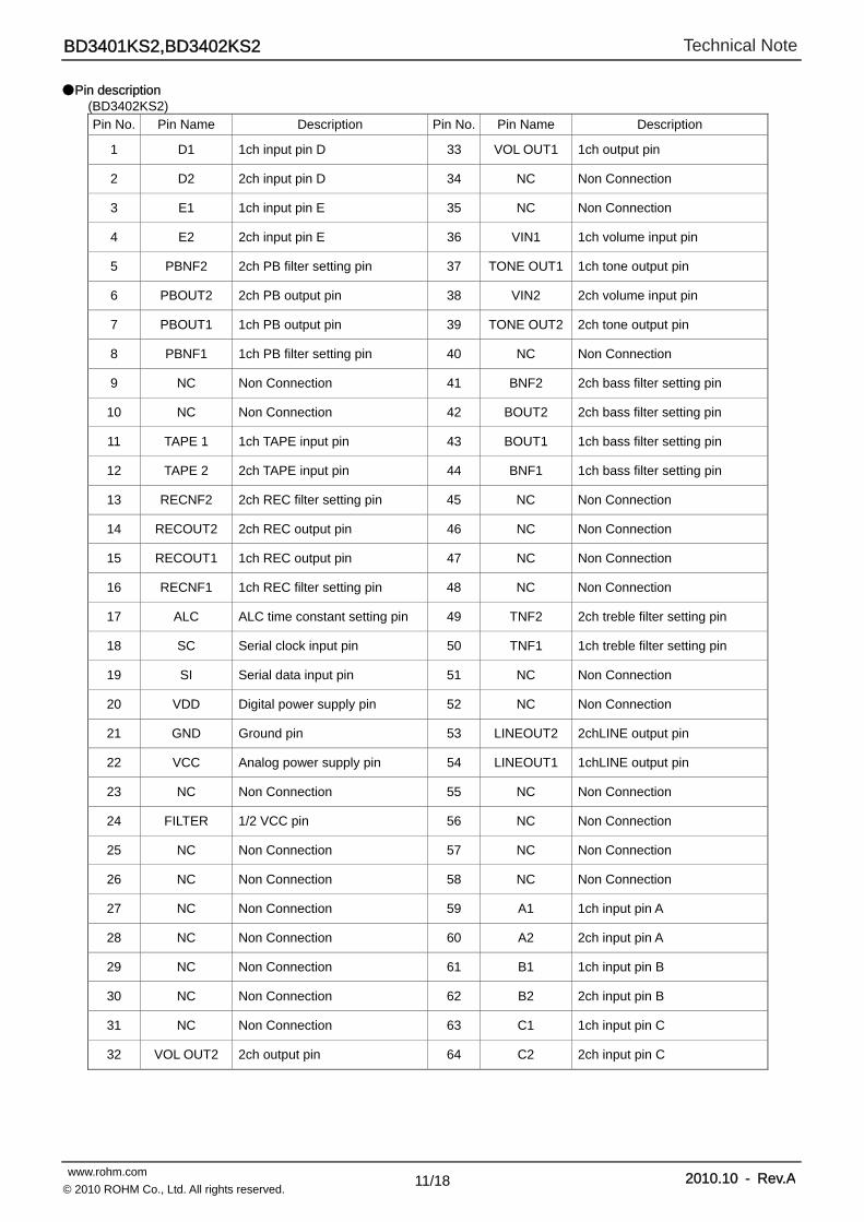
Pin description (BD3402KS2) Pin No. Pin Name Description Pin No. Pin Name Description
1 D1 1ch input pin D 33 VOL OUT1 1ch output pin
2 D2 2ch input pin D 34 NC Non Connection
3 E1 1ch input pin E 35 NC Non Connection
4 E2 2ch input pin E 36 VIN1 1ch volume input pin
5 PBNF2 2ch PB filter setting pin 37 TONE OUT1 1ch tone output pin
6 PBOUT2 2ch PB output pin 38 VIN2 2ch volume input pin
7 PBOUT1 1ch PB output pin 39 TONE OUT2 2ch tone output pin
8 PBNF1 1ch PB filter setting pin 40 NC Non Connection
9 NC Non Connection 41 BNF2 2ch bass filter setting pin
10 NC Non Connection 42 BOUT2 2ch bass filter setting pin
11 TAPE 1 1ch TAPE input pin 43 BOUT1 1ch bass filter setting pin
12 TAPE 2 2ch TAPE input pin 44 BNF1 1ch bass filter setting pin
13 RECNF2 2ch REC filter setting pin 45 NC Non Connection
14 RECOUT2 2ch REC output pin 46 NC Non Connection
15 RECOUT1 1ch REC output pin 47 NC Non Connection
16 RECNF1 1ch REC filter setting pin 48 NC Non Connection
17 ALC ALC time constant setting pin 49 TNF2 2ch treble filter setting pin
18 SC Serial clock input pin 50 TNF1 1ch treble filter setting pin
19 SI Serial data input pin 51 NC Non Connection
20 VDD Digital power supply pin 52 NC Non Connection
21 GND Ground pin 53 LINEOUT2 2chLINE output pin
22 VCC Analog power supply pin 54 LINEOUT1 1chLINE output pin
23 NC Non Connection 55 NC Non Connection
24 FILTER 1/2 VCC pin 56 NC Non Connection
25 NC Non Connection 57 NC Non Connection
26 NC Non Connection 58 NC Non Connection
27 NC Non Connection 59 A1 1ch input pin A
28 NC Non Connection 60 A2 2ch input pin A
29 NC Non Connection 61 B1 1ch input pin B
30 NC Non Connection 62 B2 2ch input pin B
31 NC Non Connection 63 C1 1ch input pin C
32 VOL OUT2 2ch output pin 64 C2 2ch input pin C
Technical Note
12/18 www.rohm.com 2010.10 - Rev.A
© 2010 ROHM Co., Ltd. All rights reserved.
BD3401KS2,BD3402KS2
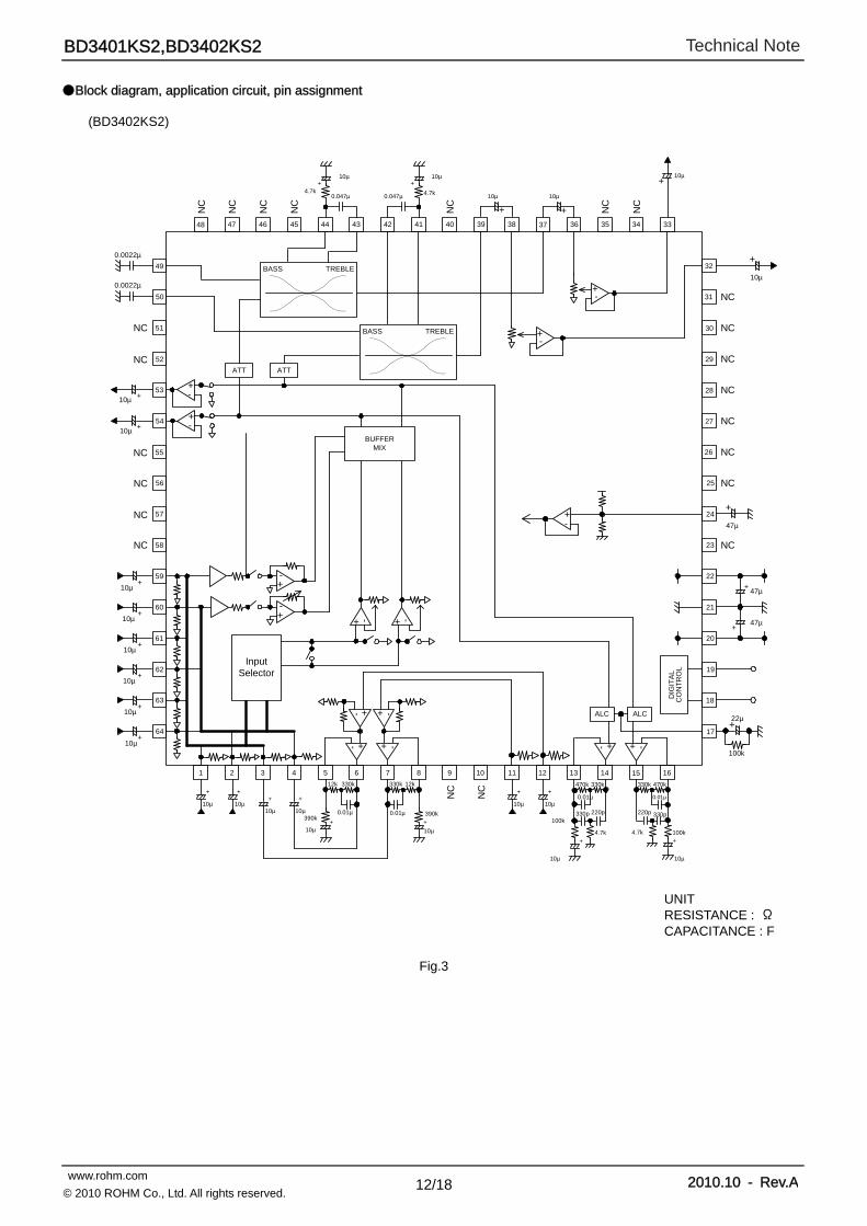
Block diagram, application circuit, pin assignment
(BD3402KS2)
Fig.3
UNIT RESISTANCE : Ω CAPACITANCE : F
1 2 3 4 5 6 7 8 9 10 11 12 13 14
64
63
62
61
60
59
58
57
56
55
54
53
52
51
46 45 44 43 42 41 40 39 38 37 36 35 34 33
17
18
19
20
21
22
23
24
25
26
27
28
29
30
15 16
48 47
50
49
31
32
DIG
ITA
LC
ON
TR
OL
ATT ATT+-
+-
+ -+ -
+ - + -
+- + -
+-
ALC ALC
+-
InputSelector
BUFFERMIX
+-
+-
+-
+-
+-
BASS TREBLE
BASS TREBLE
+ +
+
+
+
+
+
+
++
++
++
++
+
+
+
+
+
+
+
+
NC
NC
NC
NC
NC
NC
NC
NC
NC
NC
NC
NC
NC
NC
NC
NC
NC
NC
NC
NC
NC
+ +
10µ
0.047µ0.047µ
10µ
10µ10µ
10µ10µ
4.7k 4.7k
47µ
47µ
47µ
22µ
100k
100k
10µ10µ
10µ
390k390k
10µ
10µ10µ10µ10µ
10µ
10µ
10µ
10µ
10µ
10µ
10µ
10µ
0.0022µ
0.0022µ
10µ
+
4.7k
330p 220p
470k 330k
+
330k 470k
0.01µ
220p 330p
4.7k 100k
10µ
0.01µ
0.01µ 0.01µ
330k330k 12k12k
NC
NC
Technical Note
13/18 www.rohm.com 2010.10 - Rev.A
© 2010 ROHM Co., Ltd. All rights reserved.
BD3401KS2,BD3402KS2
0.001
0.01
0.1
1
10
0.001 0.01 0.1 1 10
INPUT VOLTAGE(Vrms)
OU
TP
UT
VO
LT
AG
E(V
rms)
-15
-10
-5
0
5
10
15
10 100 1000 10000 100000
FREQUENCY(Hz)
GA
IN(d
B)
+8dB(100Hz)
-8dB(100Hz)
-8dB~+8dB2dB/step
0.001
0.01
0.1
1
10
0.001 0.01 0.1 1 10
OUTPUT VOLTAGE(Vrms)
TH
D+
N(%
)
0
5
10
15
20
25
30
35
0 2 4 6 8 10
VCC(V)
ICC
(mA
)
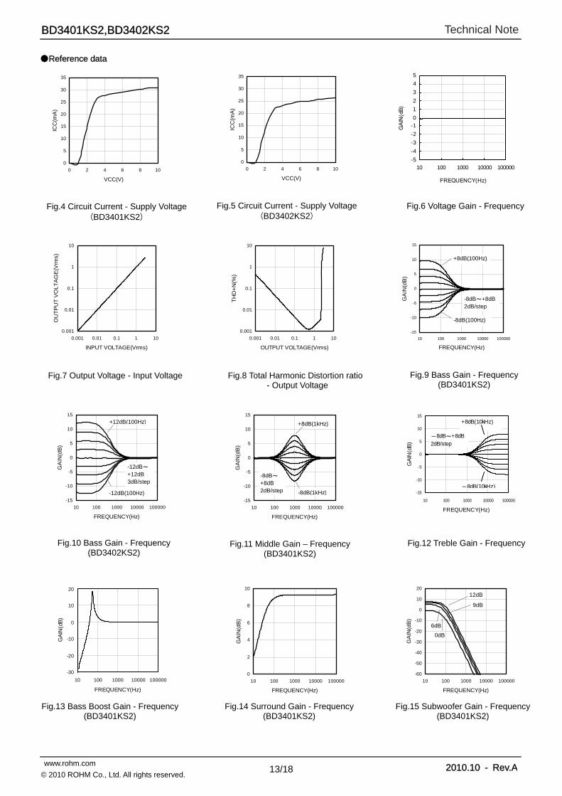
Fig.4 Circuit Current - Supply Voltage (BD3401KS2)
0
5
10
15
20
25
30
35
0 2 4 6 8 10
VCC(V)
ICC
(mA
)
Fig.5 Circuit Current - Supply Voltage (BD3402KS2)
Fig.6 Voltage Gain - Frequency
Fig.7 Output Voltage - Input Voltage Fig.9 Bass Gain - Frequency (BD3401KS2)
Fig.8 Total Harmonic Distortion ratio - Output Voltage
-15
-10
-5
0
5
10
15
10 100 1000 10000 100000
FREQUENCY(Hz)
GA
IN(d
B)
+12dB(100Hz)
-12dB(100Hz)
-12dB~+12dB3dB/step
-15
-10
-5
0
5
10
15
10 100 1000 10000 100000
FREQUENCY(Hz)
GA
IN(d
B)
+8dB(1kHz)
-8dB(1kHz)
-8dB~+8dB2dB/step -15
-10
-5
0
5
10
15
10 100 1000 10000 100000
FREQUENCY(Hz)
GA
IN(d
B)
+8dB(10kHz)
-8dB(10kHz)
-8dB~+8dB2dB/step
Fig.12 Treble Gain - Frequency Fig.11 Middle Gain – Frequency (BD3401KS2)
Fig.10 Bass Gain - Frequency(BD3402KS2)
-30
-20
-10
0
10
20
10 100 1000 10000 100000
FREQUENCY(Hz)
GA
IN(d
B)
0
2
4
6
8
10
10 100 1000 10000 100000
FREQUENCY(Hz)
GA
IN(d
B)
-60
-50
-40
-30
-20
-10
0
10
20
10 100 1000 10000 100000
FREQUENCY(Hz)
GA
IN(d
B)
0dB
6dB
9dB
12dB
Fig.13 Bass Boost Gain - Frequency (BD3401KS2)
Fig.14 Surround Gain - Frequency (BD3401KS2)
Fig.15 Subwoofer Gain - Frequency (BD3401KS2)
Reference data
-5
-4
-3
-2
-10
1
2
3
4
5
10 100 1000 10000 100000
FREQUENCY(Hz)
GAI
N(d
B)
Technical Note
14/18 www.rohm.com 2010.10 - Rev.A
© 2010 ROHM Co., Ltd. All rights reserved.
BD3401KS2,BD3402KS2
0
10
20
30
40
50
60
70
80
90
10 100 1000 10000 100000
FREQUENCY(Hz)
GA
IN(d
B)
0.01
0.1
1
10
0.0001 0.001 0.01
INPUT VOLTAGE(Vrms)
OU
TP
UT
VO
LT
AG
E(V
rms)
0.01
0.1
1
10
0.1 1 10
OUTPUT VOLTAGE(Vrms)
TH
D+
N(%
)
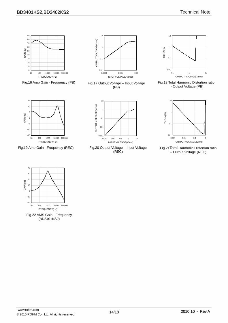
Fig.16 Amp Gain - Frequency (PB) Fig.17 Output Voltage – Input Voltage (PB)
Fig.18 Total Harmonic Distortion ratio - Output Voltage (PB)
-15
-10
-5
0
5
10
15
10 100 1000 10000 100000
FREQUENCY(Hz)
GA
IN(d
B)
0.001
0.01
0.1
1
10
0.001 0.01 0.1 1 10
INPUT VOLTAGE(Vrms)
OU
TP
UT
VO
LT
AG
E(V
rms)
0.01
0.1
1
10
0.001 0.01 0.1 1
OUTPUT VOLTAGE(Vrms)
TH
D+
N(%
)
-20
-10
0
10
20
30
40
10 100 1000 10000 100000
FREQUENCY(Hz)
GA
IN(d
B)
Fig.19 Amp Gain - Frequency (REC) Fig.20 Output Voltage – Input Voltage (REC)
Fig.21Total Harmonic Distortion ratio – Output Voltage (REC)
Fig.22 AMS Gain - Frequency (BD3401KS2)
Technical Note
15/18 www.rohm.com 2010.10 - Rev.A
© 2010 ROHM Co., Ltd. All rights reserved.
BD3401KS2,BD3402KS2
Notes for use 1) Numbers and data in entries are representative design values and are not guaranteed values of the items.
2) Although ROHM is confident that the example application circuit reflects the best possible recommendations, be sure to verify circuit characteristics for your particular application. Modification of constants for other externally connected circuits may cause variations in both static and transient characteristics for external components as well as this Rohm IC. Allow for sufficient margins when determining circuit constants.
3) Absolute maximum ratings Use of the IC in excess of absolute maximum ratings, such as the applied voltage or operating temperature range (Topr), may result in IC damage. Assumptions should not be made regarding the state of the IC (short mode or open mode) when such damage is suffered. A physical safety measure, such as a fuse, should be implemented when using the IC at times where the absolute maximum ratings may be exceeded.
4) GND potential Ensure a minimum GND pin potential in all operating conditions. Make sure that no pins are at a voltage below the GND at any time, regardless of whether it is a transient signal or not.
5) Thermal design Perform thermal design, in which there are adequate margins, by taking into account the permissible dissipation (Pd) in actual states of use.
6) Short circuit between terminals and erroneous mounting Pay attention to the assembly direction of the ICs. Wrong mounting direction or shorts between terminals, GND, or other components on the circuits, can damage the IC.
7) Operation in strong electromagnetic field Using the ICs in a strong electromagnetic field can cause operation malfunction.
8) Serial control For the SC and SI terminals, the wiring and layout patterns should be routed as not to cause interference with the analog-signal-related lines.
9) Power ON/OFF At power ON/OFF, a shock sound will be generated and, therefore, MUTE shall be applied.
10) Start-up sequence of the power supplies VDD and VCC should be turned on simultaneously or VDD first, followed by VCC.
11) Function switching (BD3401KS2)
For all functions except Master Volume, Treble, Middle, Bass, Surround, and Bass Boost, MUTE must be applied during setup.
(BD3402KS2) For all the functions except Master Volume, Treble and Bass, MUTE must be applied during setup..
12) Power-ON Reset A built-in circuit for performing initialization inside the IC at power-ON is provided. In unstable systems it is recommended that the data shall be sent to all the addresses during power-ON, until this operation cycle is completed. Mute should be applied during this cycle.
Function Initial State BD3401KS2 BD3402KS2
Input Selector MUTE
Input Gain -5dB
Volume 0dB
Treble 0dB
Bass 0dB
Middle 0dB -
TONE ATT 0dB
Subwoofer 0dB -
MUX STEREO
Mixing OFF
Mixing Gain 3dB
PLAY BACK TAPE A No selector
REC OFF
LINE OFF
MIC OFF -
Bass Boost OFF -
Surround OFF -
AMS OFF -
ALC OFF
Vocal Fader OFF -
Technical Note
16/18 www.rohm.com 2010.10 - Rev.A
© 2010 ROHM Co., Ltd. All rights reserved.
BD3401KS2,BD3402KS2
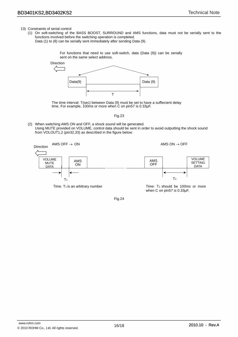
13) Constraints of serial control
(1) On soft-switching of the BASS BOOST, SURROUND and AMS functions, data must not be serially sent to the functions involved before the switching operation is completed. Data (1) to (8) can be serially sent immediately after sending Data (9).
Fig.23
(2) When switching AMS ON and OFF, a shock sound will be generated. Using MUTE provided on VOLUME, control data should be sent in order to avoid outputting the shock sound from VOLOUT1,2 (pin32,33) as described in the figure below:
Fig.24
T
Data(9) Data (9)
Direction
For functions that need to use soft-switch, data (Data (9)) can be serially sent on the same select address.
The time interval: T(sec) between Data (9) must be set to have a suffiecient delay time. For example, 100ms or more when C on pin57 is 0.33µF.
VOLUME MUTE DATA
Direction
AMSOFF
T2
VOLUME SETTING
DATA
T1
AMS ON
AMS OFF ON AMS ON OFF
Time: T1 is an arbitrary number
Time: T2 should be 100ms or more when C on pin57 is 0.33µF.
Technical Note
17/18 www.rohm.com 2010.10 - Rev.A
© 2010 ROHM Co., Ltd. All rights reserved.
BD3401KS2,BD3402KS2
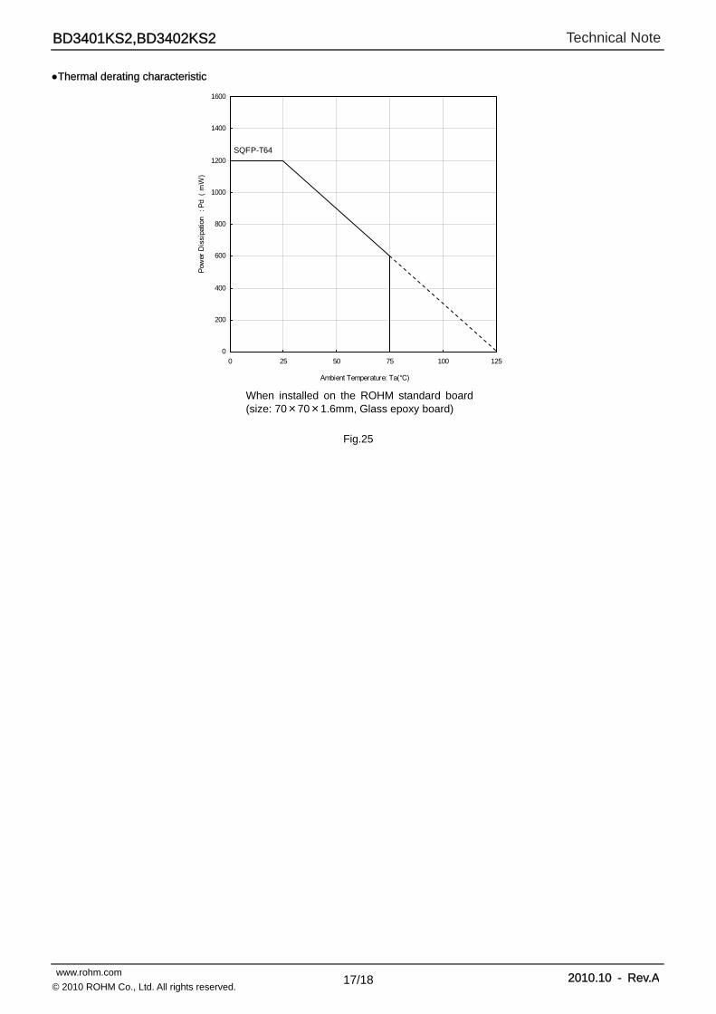
Thermal derating characteristic
Fig.25
When installed on the ROHM standard board (size: 70×70×1.6mm, Glass epoxy board)
0
200
400
600
800
1000
1200
1400
1600
0 25 50 75 100 125
Ambient Temperature: Ta()
Pow
er D
issi
patio
n :
Pd
(m
W)
SQFP-T64
Technical Note
18/18 www.rohm.com 2010.10 - Rev.A
© 2010 ROHM Co., Ltd. All rights reserved.
BD3401KS2,BD3402KS2
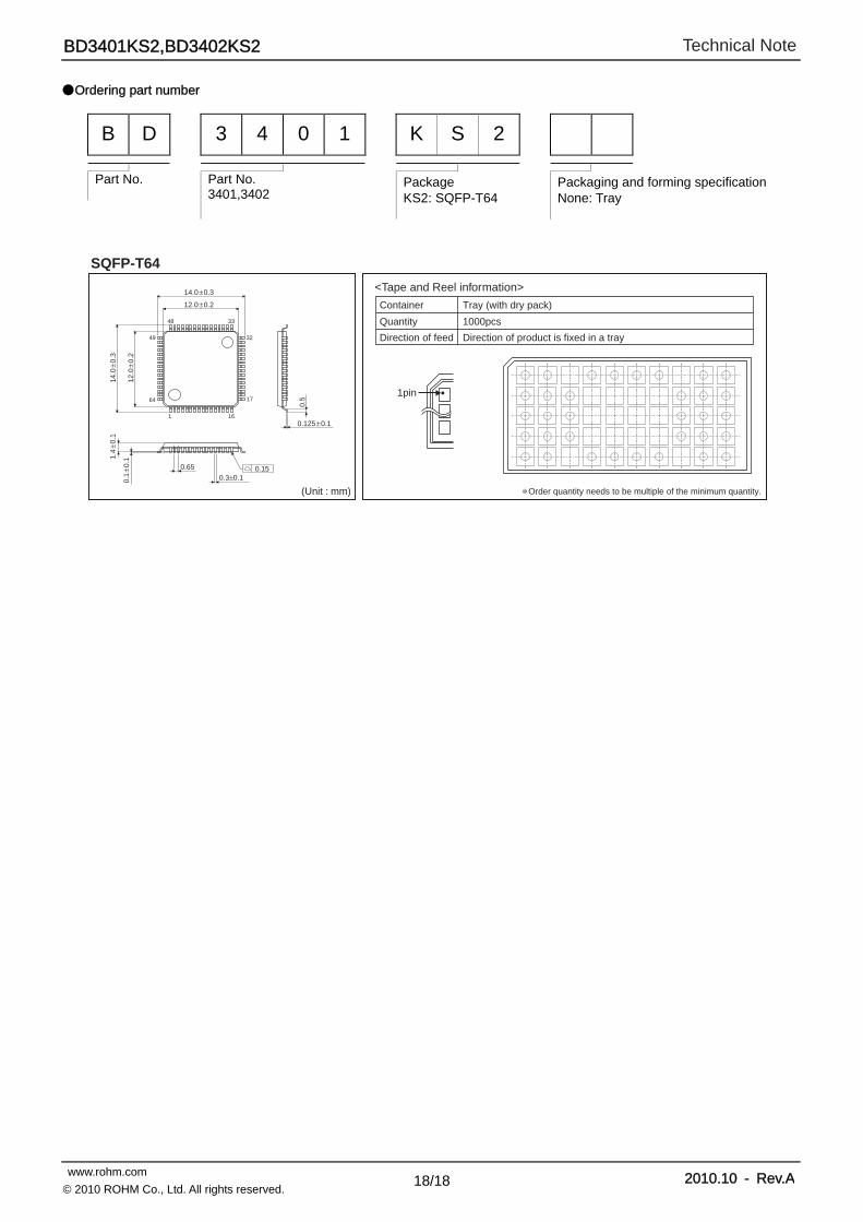
Ordering part number
B D 3 4 0 1 K S 2
Part No. Part No. 3401,3402
Package KS2: SQFP-T64
Packaging and forming specification None: Tray
∗ Order quantity needs to be multiple of the minimum quantity.
<Tape and Reel information>
Tray (with dry pack)Container
Quantity
Direction of feed
1000pcs
Direction of product is fixed in a tray
1pin
(Unit : mm)
SQFP-T64
32
64 17
49
48 33
1 16
0.15
1.4
±0.1
14.0±0.3
14.0
±0.3
0.5
0.3±0.1
0.125±0.1
12.0±0.2
0.65
12.0
±0.2
0.1
±0.1
DatasheetDatasheet
Notice - GE Rev.002© 2014 ROHM Co., Ltd. All rights reserved.
Notice Precaution on using ROHM Products
1. Our Products are designed and manufactured for application in ordinary electronic equipments (such as AV equipment, OA equipment, telecommunication equipment, home electronic appliances, amusement equipment, etc.). If you intend to use our Products in devices requiring extremely high reliability (such as medical equipment (Note 1), transport equipment, traffic equipment, aircraft/spacecraft, nuclear power controllers, fuel controllers, car equipment including car accessories, safety devices, etc.) and whose malfunction or failure may cause loss of human life, bodily injury or serious damage to property (“Specific Applications”), please consult with the ROHM sales representative in advance. Unless otherwise agreed in writing by ROHM in advance, ROHM shall not be in any way responsible or liable for any damages, expenses or losses incurred by you or third parties arising from the use of any ROHM’s Products for Specific Applications.
(Note1) Medical Equipment Classification of the Specific Applications JAPAN USA EU CHINA
CLASSⅢ CLASSⅢ
CLASSⅡb CLASSⅢ
CLASSⅣ CLASSⅢ
2. ROHM designs and manufactures its Products subject to strict quality control system. However, semiconductor
products can fail or malfunction at a certain rate. Please be sure to implement, at your own responsibilities, adequate safety measures including but not limited to fail-safe design against the physical injury, damage to any property, which a failure or malfunction of our Products may cause. The following are examples of safety measures:
[a] Installation of protection circuits or other protective devices to improve system safety [b] Installation of redundant circuits to reduce the impact of single or multiple circuit failure
3. Our Products are designed and manufactured for use under standard conditions and not under any special or extraordinary environments or conditions, as exemplified below. Accordingly, ROHM shall not be in any way responsible or liable for any damages, expenses or losses arising from the use of any ROHM’s Products under any special or extraordinary environments or conditions. If you intend to use our Products under any special or extraordinary environments or conditions (as exemplified below), your independent verification and confirmation of product performance, reliability, etc, prior to use, must be necessary:
[a] Use of our Products in any types of liquid, including water, oils, chemicals, and organic solvents [b] Use of our Products outdoors or in places where the Products are exposed to direct sunlight or dust [c] Use of our Products in places where the Products are exposed to sea wind or corrosive gases, including Cl2,
H2S, NH3, SO2, and NO2
[d] Use of our Products in places where the Products are exposed to static electricity or electromagnetic waves [e] Use of our Products in proximity to heat-producing components, plastic cords, or other flammable items [f] Sealing or coating our Products with resin or other coating materials [g] Use of our Products without cleaning residue of flux (even if you use no-clean type fluxes, cleaning residue of
flux is recommended); or Washing our Products by using water or water-soluble cleaning agents for cleaning residue after soldering
[h] Use of the Products in places subject to dew condensation
4. The Products are not subject to radiation-proof design. 5. Please verify and confirm characteristics of the final or mounted products in using the Products. 6. In particular, if a transient load (a large amount of load applied in a short period of time, such as pulse. is applied,
confirmation of performance characteristics after on-board mounting is strongly recommended. Avoid applying power exceeding normal rated power; exceeding the power rating under steady-state loading condition may negatively affect product performance and reliability.
7. De-rate Power Dissipation (Pd) depending on Ambient temperature (Ta). When used in sealed area, confirm the actual
ambient temperature. 8. Confirm that operation temperature is within the specified range described in the product specification. 9. ROHM shall not be in any way responsible or liable for failure induced under deviant condition from what is defined in
this document.
Precaution for Mounting / Circuit board design 1. When a highly active halogenous (chlorine, bromine, etc.) flux is used, the residue of flux may negatively affect product
performance and reliability. 2. In principle, the reflow soldering method must be used; if flow soldering method is preferred, please consult with the
ROHM representative in advance. For details, please refer to ROHM Mounting specification

DatasheetDatasheet
Notice - GE Rev.002© 2014 ROHM Co., Ltd. All rights reserved.
Precautions Regarding Application Examples and External Circuits 1. If change is made to the constant of an external circuit, please allow a sufficient margin considering variations of the
characteristics of the Products and external components, including transient characteristics, as well as static characteristics.
2. You agree that application notes, reference designs, and associated data and information contained in this document
are presented only as guidance for Products use. Therefore, in case you use such information, you are solely responsible for it and you must exercise your own independent verification and judgment in the use of such information contained in this document. ROHM shall not be in any way responsible or liable for any damages, expenses or losses incurred by you or third parties arising from the use of such information.
Precaution for Electrostatic
This Product is electrostatic sensitive product, which may be damaged due to electrostatic discharge. Please take proper caution in your manufacturing process and storage so that voltage exceeding the Products maximum rating will not be applied to Products. Please take special care under dry condition (e.g. Grounding of human body / equipment / solder iron, isolation from charged objects, setting of Ionizer, friction prevention and temperature / humidity control).
Precaution for Storage / Transportation 1. Product performance and soldered connections may deteriorate if the Products are stored in the places where:
[a] the Products are exposed to sea winds or corrosive gases, including Cl2, H2S, NH3, SO2, and NO2 [b] the temperature or humidity exceeds those recommended by ROHM [c] the Products are exposed to direct sunshine or condensation [d] the Products are exposed to high Electrostatic
2. Even under ROHM recommended storage condition, solderability of products out of recommended storage time period may be degraded. It is strongly recommended to confirm solderability before using Products of which storage time is exceeding the recommended storage time period.
3. Store / transport cartons in the correct direction, which is indicated on a carton with a symbol. Otherwise bent leads
may occur due to excessive stress applied when dropping of a carton. 4. Use Products within the specified time after opening a humidity barrier bag. Baking is required before using Products of
which storage time is exceeding the recommended storage time period.
Precaution for Product Label QR code printed on ROHM Products label is for ROHM’s internal use only.
Precaution for Disposition When disposing Products please dispose them properly using an authorized industry waste company.
Precaution for Foreign Exchange and Foreign Trade act Since our Products might fall under controlled goods prescribed by the applicable foreign exchange and foreign trade act, please consult with ROHM representative in case of export.
Precaution Regarding Intellectual Property Rights 1. All information and data including but not limited to application example contained in this document is for reference
only. ROHM does not warrant that foregoing information or data will not infringe any intellectual property rights or any other rights of any third party regarding such information or data. ROHM shall not be in any way responsible or liable for infringement of any intellectual property rights or other damages arising from use of such information or data.:
2. No license, expressly or implied, is granted hereby under any intellectual property rights or other rights of ROHM or any
third parties with respect to the information contained in this document.
Other Precaution 1. This document may not be reprinted or reproduced, in whole or in part, without prior written consent of ROHM. 2. The Products may not be disassembled, converted, modified, reproduced or otherwise changed without prior written
consent of ROHM. 3. In no event shall you use in any way whatsoever the Products and the related technical information contained in the
Products or this document for any military purposes, including but not limited to, the development of mass-destruction weapons.
4. The proper names of companies or products described in this document are trademarks or registered trademarks of
ROHM, its affiliated companies or third parties.
DatasheetDatasheet
Notice – WE Rev.001© 2014 ROHM Co., Ltd. All rights reserved.
General Precaution 1. Before you use our Pro ducts, you are requested to care fully read this document and fully understand its contents.
ROHM shall n ot be in an y way responsible or liabl e for fa ilure, malfunction or acci dent arising from the use of a ny ROHM’s Products against warning, caution or note contained in this document.
2. All information contained in this docume nt is current as of the issuing date and subj ect to change without any prior
notice. Before purchasing or using ROHM’s Products, please confirm the la test information with a ROHM sale s representative.
3. The information contained in this doc ument is provi ded on an “as is” basis and ROHM does not warrant that all
information contained in this document is accurate an d/or error-free. ROHM shall not be in an y way responsible or liable for any damages, expenses or losses incurred by you or third parties resulting from inaccuracy or errors of or concerning such information.