sorting out the neural basis of consciousness
TRANSCRIPT
IEEE TRANSACTIONS ON SEMICONDUCTOR MANUFACTURING, VOL. 11, NO. 4, NOVEMBER 1998 557
Circuit Sensitivity to Interconnect VariationZhihao Lin, Member, IEEE,Costas J. Spanos,Senior Member, IEEE,Linda S. Milor, Member, IEEE,and Y. T. Lin
Abstract—Deep submicron technology makes interconnect oneof the main factors determining the circuit performance. Previouswork shows that interconnect parameters exhibit a significantamount of spatial variation. In this work, we develop approachesto study the influence of the interconnect variation on circuitperformance and to evaluate the circuit sensitivity to interconnectparameters. First, an accurate interconnect modeling techniqueis presented, and an interconnect model library is developed.Then, we explore an approach using parameterized interconnectmodels to study circuit sensitivity via a ring oscillator circuit.Finally, we present an alternative approach using statisticalexperimental design techniques to study the sensitivity of a largeand complicated circuit to interconnect variations.
Index Terms—Circuit analysis, interconnect, statistical analy-sis, worst case design.
I. INTRODUCTION
T HE CONTINUOUSLY increasing scale of integrationused in the design and processing of integrated circuits
has drawn special attention toward interconnect effects. Asthe minimum feature size in VLSI systems drops to 0.25mand below, interconnect characteristics are becoming limitingfactors on performance, since the time constant associatedwith interconnect is scaled by a smaller factor compared tothose of devices. Future chip complexity and speed advanceswill depend on the ability to model the electrical behavior ofinterconnect in an accurate and efficient fashion.
Critical path delays in circuits depend upon interconnect aswell as on device parameters. The effects of device parametervariations have been widely studied [12]–[16]. However, thesesimulations currently do not take into account the effectsof interconnect parameter variations. As a result, the yieldestimation and circuit optimization based on these studies maynot be able to provide accurate results in current and futuretechnologies, where more and more significant portions of pathdelays will result from interconnect.
With current technology, the impact of interconnect parame-ter variations on signal delays may already be quite significant[2]. Thus, it becomes necessary to comprehend and anticipatethe effects of interconnect parameter variation in the designprocess. Specifically, a methodology to asses the impact ofrandom and systematic variations in interconnect parametersto circuit performance must be developed.
Manuscript received June 11, 1998; revised March 27, 1998.Z. Lin is with NeoParadigm Lab, Inc., San Jose, CA 95134 USA (e-mail:
[email protected]).C. J. Spanos is with the Electrical Engineering and Computer Sciences
Department, University of California, Berkeley, CA 94720-1770 USA.L. S. Milor and Y. T. Lin are with Advanced Micro Devices, Inc.,
Sunnyvale, CA 94088 USA.Publisher Item Identifier S 0894-6507(98)08365-1.
A modeling framework to study the sensitivity of circuitperformance to interconnect parameter variations will allowcircuit designers to meet timing targets while taking intoaccount the random and systematic source of interconnectparameter variations. It will also help the process designersto design new technologies while taking the sensitivity infor-mation into consideration. Finally, the sensitivity study resultswill help make the circuit more robust against the variation.
Overall, the goal of this paper is to address the problemof interconnect variations, look for a methodology to modelinterconnect wires, and develop approaches to quantify andinvestigate interconnect parameter variations on circuit per-formance under current and future technologies. The ultimateobjective is to facilitate optimal circuit and process design,reduce time-to-yield, and improve the final yield.
Two approaches to study the circuit sensitivity to inter-connect parameter variations are developed in this paper.The first approach is based on a parameterized interconnectmodel library. The parameterized interconnect models allowus to manipulate interconnect parameters, and to generate acircuit description that is suitable for performance sensitivitystudy. The second approach uses statistical experimental de-sign techniques to analyze complicated circuits via simulationexperiments. The first approach is illustrated with the help ofa ring oscillator circuit, and the second approach is illustratedwith a large multiplier circuit.
II. I NTERCONNECT MODELING
A. Introduction
In order to understand and account for interconnect effectsin the design process, it is necessary to extract its parasitic pa-rameters and model the interconnection. It is essential that theelectrical behavior of interconnect is modeled accurately. Theaccuracy of interconnect models is the very basis of achievingmeaningful predictions of circuit behavior and obtain reliablesensitivity evaluations. The models should also be suitable forstatistical circuit simulation and sensitivity analysis, which isthe purpose of this work.
One approach to interconnect modeling is to constructan equivalent electrical circuit representation. The equivalentcircuits that represent the interconnections can be combinedwith the equivalent circuits that describe the active devices,and the behavior of the entire circuit can be analyzed with acircuit simulator such as HSPICE.
There are two steps to the process of constructing anequivalent circuit model for an interconnect wire. The first stepis to determine the nature of the equivalent circuit, that is, whatkinds of circuit elements are important, and how many degrees
0894–6507/98$10.00 1998 IEEE

558 IEEE TRANSACTIONS ON SEMICONDUCTOR MANUFACTURING, VOL. 11, NO. 4, NOVEMBER 1998
of freedom are required for the level of accuracy desired. Thesecond step is to determine the value associated with eachelement in the equivalent circuit.
Reference [10] claims that the equivalent circuit for anaverage length on-chip interconnection in CMOS chips canbe constructed using capacitors and resistors. In modern lossyon-chip interconnect, the inductive voltage drop is negligiblecompared to resistive voltage drop up to clock frequencies of1–2 GHz. Thus, on-chip interconnect lines may be approxi-mated by an RC line. So, throughout this work, all on-chipinterconnects are modeled as RC networks.
Once it has been determined what types of circuit elementsare required to model a particular class of on-chip intercon-nections, one must then decide how many circuit elements ofeach type are needed and evaluate the values of interconnectparasitics.
There are many ways to extract the parasitics. The applica-tions of empirical formulae to general submicron interconnectwires are rather limited because of the complexity of inter-connect configurations in multilevel submicron technology,especially in extracting the coupling capacitance. These for-mulae can not cover layout configurations having multipledielectric and metal layers. Furthermore, they are not accurateenough to capture the variations of the layout and technologyparameters of interconnect. So their applicability in our workof sensitivity study over the technology parameters is notappropriate.
In “exact” computations of electrical circuit parameters, oneappeals to the theory of electromagnetic fields; that is, “exact”computations involve the numerical analysis of two or threedimensional integral or partial-differential equations for thevalues of an electromagnetic field.
Since multilevel interconnect technologies use multiple con-ductors with different thicknesses and multiple insulators withpossibly different dielectric constants, numerical simulationsare mandatory for accurate resistance and capacitance model-ing [20]–[22]. Numerical techniques have been developed forrigorous interconnect capacitance extraction.
B. Interconnect Model Library
We have concluded the necessity of numerically based simu-lation to perform interconnect parasitics extraction. However,numerical simulation is computationally intensive and real-time simulation is too time-consuming. Furthermore, in ourapproach to perform sensitivity study, all interconnect wiresare to be modeled using closed-form analytical models, whichrequires parameterized interconnect models. To cope with thisproblem, a realistic approach is to construct a parameterizedinterconnect model library based on numerical simulations.Then the circuit description can be generated with the helpof the model library which contains models of typical two-dimensional interconnect structures. The circuit descriptionwill thus become the basis of sensitivity study and statisticalcircuit simulation.
Fig. 2 shows the flow of this interconnect modeling ap-proach and model library building. The sensitivity analysisis performed assuming that the variation of technology pa-
Fig. 1. Cross section of an interconnect structure.
Fig. 2. Interconnect modeling flow.
rameters, interlayer dielectric thickness, conductor thickness,is within about 20%1 of its nominal value for a given tech-nology. At the same time, the ranges of the layout parameters,such as metal width, interwire spacing, are set according to thedesign rules and their possible design ranges. Each parameteris divided into several levels, and a full factorial design isused to generate the simulation points for each structure. Theinput file to the numerical simulator is generated to containall the simulation points, and two dimensional simulations areperformed in batch-mode using a numerically based extractor[23] to evaluate the unit length capacitance and resistancevalues. The numerical data are then fitted to an analyticalexpression using a special curve-fitting technique which willbe discussed in more detail later.
In the following sections, we will use the structure in Fig. 1as an example to illustrate the approach in more detail.
The interconnect structure shown in Fig. 1 is defined interms of four parameters: metal width , interwire distance
, metal thickness , and thickness . The threecapacitances, , and are of interest and theirmodels are constructed. Notice that all interwire distances arethe same in this structure.
The input file to the numerical extractor Raphael is gener-ated as follows: each parameter, , and , is set at six,six, seven, and seven levels, respectively. Using a full factorialdesign, a total number of 1764 simulation points (combinationof different levels of the four parameters) are generated, andthe input file for Raphael is thus created based on these points.
1Based on this assumption, all the variations that are less than 20% oftheir normal values will be covered by the models. Though this value maynot exactly reflect the realistic situation, it does not affect the flow of thisapproach.
LIN et al.: CIRCUIT SENSITIVITY TO INTERCONNECT VARIATION 559
Analytical models are then constructed based on the simulationresults. This is discussed in the next section.
C. Curve-Fitting Technique
The objective is to create a model that mapsthe relationship between the set of parameters defining thephysical interconnect and the values of the parasitics of theinterconnect. Here is the dimensional vector representingthe capacitance and resistance to be modeled, andis the
dimensional input vector containing all the interconnectparameters. This is implemented using simple polynomialexpressions and linear regression [24].
The capacitance models can include quadratic and higherorder terms of the parameters, together with their interactionterms. In order to achieve an accurate model, the first stepis to determine the terms to be included in the final model.After the model terms have been determined, the coefficientof each term can be estimated using the least square technique.However, choosing the terms of the model is a difficult task.In this section, we present a systematic way to address thisproblem. This efficient and systematic solution is guided bythe simple physical relationships between the input variablesand the resulting capacitance.
First, we select the data points that are obtained by varyingone parameter with the other parameters fixed. Then these datapoints are fitted over this parameter using step-wise regression.This is easy since only one variable or parameter is involved.In this way, one will get a separate model related to each ofthe parameters. These models are simple polynomial functions.In some cases, nonlinear data transformations are necessaryin order to apply a linear model. Combining these separatemodels, the final model terms are easy to identify. This isillustrated as follows:
Suppose that capacitance is an unknown polynomialfunction of two variables, and . That is, .The goal is to choose the proper model terms based on discretedata points.
Let us assume that by curve-fitting over with fixed,one finds that is a linear function of , that is,
(1)
In the above equation, bothand are constants. They willtake different values when is fixed at different points. Soand are only functions of , i.e.,
and (2)
then (1) can be rewritten as
(3)
Suppose that is fitted over with fixed, and the fittingresult shows is a second order polynomial function of.Following the same argument as above, one can conclude that
can also be expressed as
(4)
Note that (3) and (4) are equivalent expressions. Since bothequations represent capacitance, which must be a continuous
function of both and , we can take the derivative ofthese two equations over , which leads to the followingexpression:
(5)Thus, the model terms of can be decided. Given
the fact that the left-hand side (LHS) of (5) does not dependon , the right-hand side (RHS) should also be independentof . Then we can conclude that , andare linear functions of , i.e.,
(6)
(7)
(8)
Here, to are constants. By substituting (6)–(8)into (4), the model terms can be easily identified and theequation can be rewritten as
(9)
To simplify the situation, the above illustration assumes thatis a linear function of when is fixed. If is a second
or higher order function of , the above explanation stillapplies on taking higher order derivatives, which will lead tosimilar results.
In practice, the above technique is used to choose the termsof the model, while the coefficients of the terms are determinedusing least squares fitting.
Though only two variables are discussed in the abovetechnique, the approach can be easily generalized to threeand more variables. Also, note that even though the abovediscussion is not a strict mathematical proof, it does provideus with some insight and guidance on data fitting in order toget an accurate capacitance model.
D. Example
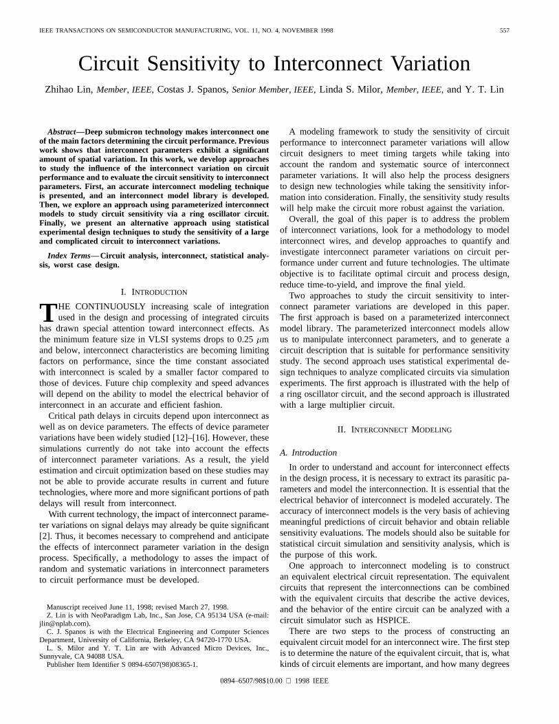
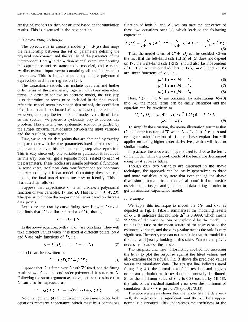
We apply this technique to model the and asdepicted in Fig. 1. Table I summarizes the modeling resultsof . It indicates that multiple is 0.9999, which means99.99% of the variation can be explained by the model. F-ratio is the ratio of the mean square of the regression to theestimated variance, and the zero p-value means the ratio is verysignificant. However, one can not conclude that the model fitsthe data well just by looking at this table. Further analysis isnecessary to assess the model.
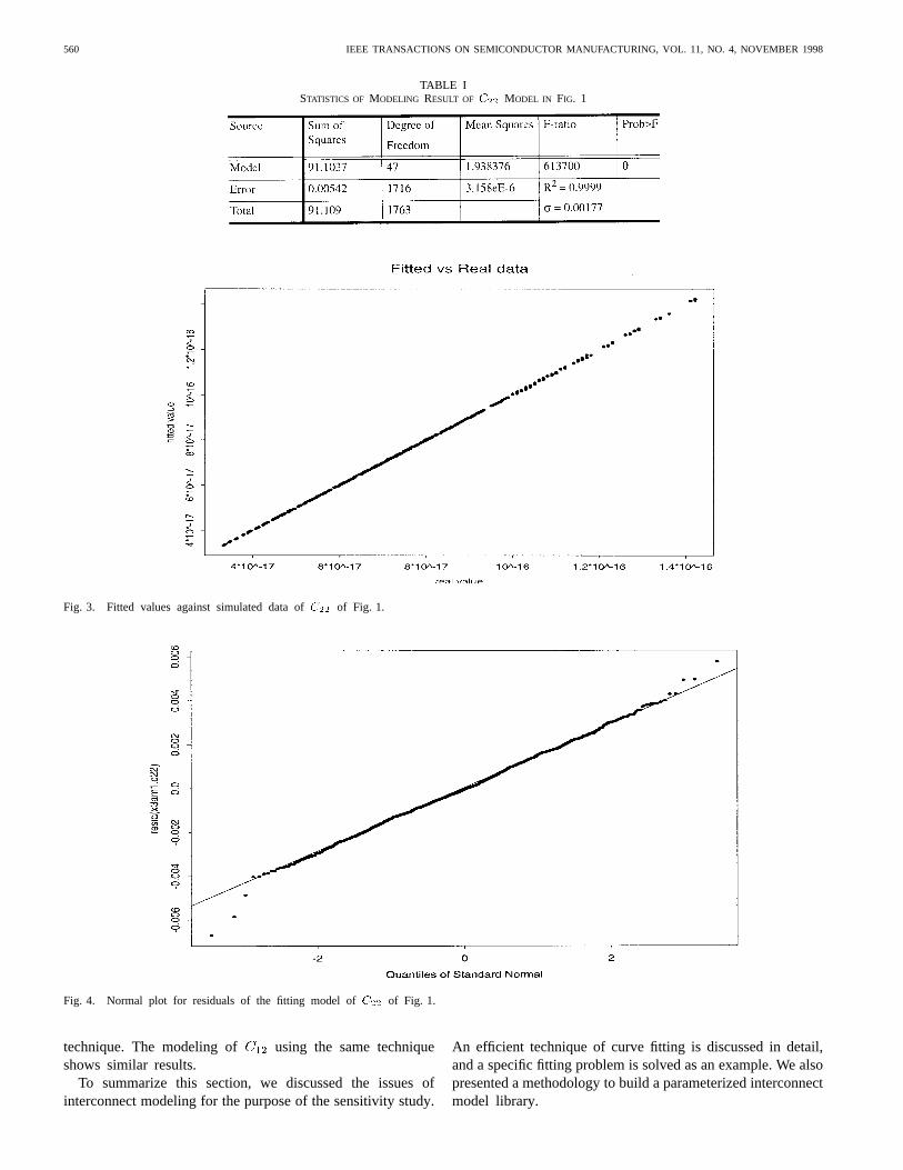
The simplest and most informative method for assessingthe fit is to plot the response against the fitted values, andalso examine the residuals. Fig. 3 shows the predicted valuesversus the simulation data. The straight line indicates goodfitting. Fig. 4 is the normal plot of the residual, and it givesno reason to doubt that the residuals are normally distributed.Since the minimum value of is 0.33 (scaled by 1E-16),the ratio of the residual standard error over the minimum ofsimulation data is just 0.5% (0.0017/0.33).
The above analysis shows that the model fits the data verywell, the regression is significant, and the residuals appearnormally distributed. This underscores the usefulness of the
560 IEEE TRANSACTIONS ON SEMICONDUCTOR MANUFACTURING, VOL. 11, NO. 4, NOVEMBER 1998
TABLE ISTATISTICS OF MODELING RESULT OF C22 MODEL IN FIG. 1
Fig. 3. Fitted values against simulated data ofC22 of Fig. 1.
Fig. 4. Normal plot for residuals of the fitting model ofC22 of Fig. 1.
technique. The modeling of using the same techniqueshows similar results.
To summarize this section, we discussed the issues ofinterconnect modeling for the purpose of the sensitivity study.
An efficient technique of curve fitting is discussed in detail,and a specific fitting problem is solved as an example. We alsopresented a methodology to build a parameterized interconnectmodel library.

LIN et al.: CIRCUIT SENSITIVITY TO INTERCONNECT VARIATION 561
Fig. 5. Overview of sensitivity study based on interconnect model library.
Based on the interconnect model library built, we are readyto develop an approach to study the circuit sensitivity tointerconnect variations. This is discussed in Section III.
III. SENSITIVITY STUDY
The models developed in last section, and the establishedrange values for interconnect parameters are the essentialingredients for the evaluation of the impact on circuit per-formance. In this section, an approach to accomplish thisevaluation will be explored, and the relationships betweeninterconnect parameter variations and circuit performance willbe developed.
The goal of statistical circuit design is to model and improveparametric yield [15]. The underlying concept is that variationsin the manufacturing process change the performance of theintegrated circuit and therefore cause the performance yieldfluctuations seen in the final test. As stated in Section I, anew approach needs to be developed since active devices andinterconnect wires are different in many aspects. To incorpo-rate interconnections into the framework, the manufacturingline variations must be mapped into the variations of bothdevices and interconnect parameters, and then be mapped intothe performance variations of circuits.
A. Methodology
An overview of the methodology to perform circuit sensi-tivity to interconnect variations is shown in Fig. 5. The basicidea is to model each interconnect wire of a circuit using theparameterized interconnect models developed in Section II,and then generate the circuit description based on a SPICEfile. The generated circuit description contains closed-formanalytical expressions for each interconnect capacitance andresistance elements, and it is the basis of the statistical circuitsimulation.
To simulate the effect of process variations on a circuit,the connection between the process parameters and the inputfile to circuit simulator must be established. So the RCmodel for each interconnect wire should be expressed interms of the interconnect parameters. With the help of theinterconnect model library developed in the last section, the
Fig. 6. Circuit diagram of a ring oscillator.
total capacitance and resistance of each interconnect wire canbe easily described given the length of each wire, thus an RCmodel of each wire is built. The resulting description of theinterconnect wires in a circuit usually takes the form of an RCmesh because of the coupling capacitance among neighboringwires.
We use the HSPICE circuit simulator to estimate circuitperformance. Our work does not use formal optimizationtechniques to improve yield as the focus of this work is on thesensitivity analysis. More specifically, our goal is to determinethe impact of interconnect related process parameters onperformance.
The variation ranges of interconnect parameters form a mul-tidimensional region which is referred to as aparameter space.This parameter space will be mapped to the variation ranges ofthe performance which is referred to as theperformance space.
B. Case Study: Ring Oscillator Circuit
A ring oscillator was used to explore the sensitivity analysisapproach. Fig. 6 shows part of the circuit diagram of the ringoscillator, which emphasizes the interconnect wires betweenstages. The loading of the circuit is dominated by interconnectwires, as indicated in Fig. 6. The interconnection length foreach stage is 180m, and is divided into six fingers. Three ofthe fingers are next to previous stage fingers and the other threeare next to next stage fingers, so there is a heavy capacitivecoupling effect between neighboring stages.
The ring oscillator circuit used in this study has nine stages,with fan-out of 2. However, the design is such that significantloading is contributed by interconnect wires. In this way, thesignal delay between each stage is mainly determined bythe interconnect capacitance and resistance.
First, the SPICE netlist is generated based on its layout usingthe extraction tool. Then, it is modified so that interconnectwires of the circuit are modeled in terms of the interconnectparameters. For example, coupling capacitance is modeledexplicitly in terms of the length and distance of the wires.The regularity of this relatively simple ring oscillator circuitmakes it easier to accomplish this modification. The fingers areparallel and have the same width and the same interwire space.By generating the circuit description in this way, a direct linkbetween the circuit performance and interconnect parametersis established.
562 IEEE TRANSACTIONS ON SEMICONDUCTOR MANUFACTURING, VOL. 11, NO. 4, NOVEMBER 1998
Fig. 7. Ring oscillator delay versus metal width.
Fig. 8. Ring oscillator delay versus interwire spacing.
C. Results and Analysis
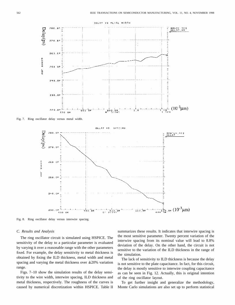
The ring oscillator circuit is simulated using HSPICE. Thesensitivity of the delay to a particular parameter is evaluatedby varying it over a reasonable range with the other parametersfixed. For example, the delay sensitivity to metal thickness isobtained by fixing the ILD thickness, metal width and metalspacing and varying the metal thickness over20% variationrange.
Figs. 7–10 show the simulation results of the delay sensi-tivity to the wire width, interwire spacing, ILD thickness andmetal thickness, respectively. The roughness of the curves iscaused by numerical discretization within HSPICE. Table II
summarizes these results. It indicates that interwire spacing isthe most sensitive parameter. Twenty percent variation of theinterwire spacing from its nominal value will lead to 8.8%deviation of the delay. On the other hand, the circuit is notsensitive to the variation of the ILD thickness in the range ofthe simulation.
The lack of sensitivity to ILD thickness is because the delayis not sensitive to the plate capacitance. In fact, for this circuit,the delay is mostly sensitive to interwire coupling capacitanceas can be seen in Fig. 12. Actually, this is original intentionof the ring oscillator layout.
To get further insight and generalize the methodology,Monte Carlo simulations are also set up to perform statistical

LIN et al.: CIRCUIT SENSITIVITY TO INTERCONNECT VARIATION 563
Fig. 9. Ring oscillator delay versus ILD thickness. The layout of the ring oscillator is designed such that the delay is mainly determined by the couplingcapacitance between neighboring wires instead of plate capacitance.
Fig. 10. Ring oscillator delay versus metal thickness.
TABLE IIRESULTS OF SENSITIVITY STUDY OF RING OSCILLATOR
analysis. These statistical simulations closely reflect whathappens in the real world. The simulation results establisha connection between performance spread and the variation ofparameters.
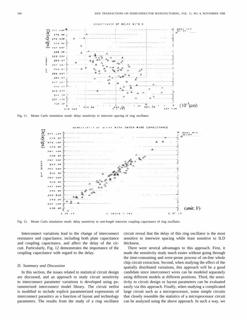
The Monte Carlo simulation is performed based on theassumption that all interconnect parameters (there are fourparameters in this study) are normally distributed withequal to 20% of their nominal values. These results are con-sistent with the previous deterministic analysis. Particularly,Fig. 11 shows the significant sensitivity of interwire spacingwith respect to the delay.
564 IEEE TRANSACTIONS ON SEMICONDUCTOR MANUFACTURING, VOL. 11, NO. 4, NOVEMBER 1998
Fig. 11. Monte Carlo simulation result: delay sensitivity to interwire spacing of ring oscillator.
Fig. 12. Monte Carlo simulation result: delay sensitivity to unit-length interwire coupling capacitance of ring oscillator.
Interconnect variations lead to the change of interconnectresistance and capacitance, including both plate capacitanceand coupling capacitance, and affect the delay of the cir-cuit. Particularly, Fig. 12 demonstrates the importance of thecoupling capacitance with regard to the delay.
D. Summary and Discussion
In this section, the issues related to statistical circuit designare discussed, and an approach to study circuit sensitivityto interconnect parameter variations is developed using pa-rameterized interconnect model library. The circuit netlistis modified to include explicit parameterized expressions ofinterconnect parasitics as a function of layout and technologyparameters. The results from the study of a ring oscillator
circuit reveal that the delay of this ring oscillator is the mostsensitive to interwire spacing while least sensitive to ILDthickness.
There were several advantages to this approach. First, itmade the sensitivity study much easier without going throughthe time-consuming and error-prone process of on-line wholechip circuit extraction. Second, when studying the effect of thespatially distributed variations, this approach will be a goodcandidate since interconnect wires can be modeled separatelyusing different models at different positions. Third, the sensi-tivity to circuit design or layout parameters can be evaluatedeasily via this approach. Finally, when studying a complicatedlarge circuit such as a microprocessor, some simple circuitsthat closely resemble the statistics of a microprocessor circuitcan be analyzed using the above approach. In such a way, we

LIN et al.: CIRCUIT SENSITIVITY TO INTERCONNECT VARIATION 565
Fig. 13. The methodology of sensitivity study using statistical experimentdesign.
can evaluate and forecast the performance spread of the mi-croprocessor resulting from interconnect parameter variationsbefore the manufacturing of the product die.
However, there are some limitations to this approach. Itrequires manual construction of an RC model for each in-terconnect wire, so it is not very suitable for studying acomplicated and irregular, circuit directly. It is inefficient tomanually model the whole circuit. So, an alternative approachis developed in next section to study the impact of processvariations of interconnect technology parameters on circuitperformance.
IV. SENSITIVITY STUDY USING
STATISTICAL EXPERIMENTAL DESIGN
In this section, we will show how a sensitivity analysis couldbe carried out for a complex circuit that does not have theregularity.
As technology advances, the number of interconnect layersincreases, and the configuration of interconnect becomes moreand more complicated. Since there are many parameters ofinterest in multilayer interconnect technology, and the cost offull-chip simulation is very high, statistical experiment designtechniques become very useful in carrying out the computersimulations that explore the sensitivities of interest.
A. Methodology
The basic idea of this approach is that given the variationranges of the technology parameters, the technology file whichcontains all the technology parameters is revised accordingto the experimental design. Then, different circuit descriptionfiles are generated from each revised technology files. Thecircuit description files are HSPICE decks. They are fed intothe circuit simulator to evaluate the performance of the circuit.Specifically, the flow of this approach is shown in Fig. 13 andis listed as follows.
1) Design experiments with interconnect parameter vari-ables, and construct the design matrix.
2) Revise the technology file based on the design matrixfor each designed experiment.
3) Extract the parasitics of the circuit from the layout giveneach revised technology file, and generate an HSPICEdeck.
4) Convert the HSPICE deck to Epic compatible input file.Run Pathmill2 to identify the critical paths and evaluatethe delay of each critical path.
5) Perform statistical analysis based on the simulationresults of the extracted critical paths. Model the delayof the critical path.
A 32-bit shift-and-add multiplier circuit is used as a studycase. This circuit has three metal layers and one poly layer,as shown in Fig. 14. The variables of interest are listed asfollows.
Thickness of poly, metal1, metal2, andmetal3, respectively.Field oxide thickness.ILD thickness between poly and metal1ILD thickness between metal1 and metal2.ILD thickness between metal2 and metal3.
B. Screening Experiment
The purpose of the screening experiment is to investigatethe most sensitive and important factors among the eightparameters listed above, with respect to the performancevariation. The range of each parameter was chosen to effec-tively encompass its possible variation range during regularproduction. A full factorial experiment to determine all effectsand interactions for the eight factors would require 2, or 256experiments. In order to reduce the experimental budget andsimulation cost, the effects of higher order interactions wereneglected and a 2 fractional factorial design requiring only16 runs was performed.
The analysis of screening experiment results revealed thatonly two of the eight variables have large effects3 on the circuitperformance: ILD thickness between poly and metal 1 and ILDthickness between metal1 and metal2, i.e.,and .
The result also shows that interconnect wires play animportant role in determining the critical path delay of thismultiplier. This will be further analyzed in the subsequentsubsections.
Since variation of circuit performance is mainly due to thevariation of capacitance, the results show thatand canexplain most of the variations of the capacitance.
It should be noted that the above result is much circuitdependent, and even layout dependent to some extent. Sodifferent categories of circuits will exhibit different sensitiv-ities to interconnect parameters. Even for the same circuit,the sensitivity analysis results may be different with differenttechnologies, or with the same technology but different lay-outs. This is because the routing layers and length of eachlayer may be much different. So the results from the analysis
2Pathmill is a CAD tool from Epic Inc., used to identify the critical pathsof a circuit.
3Since this is a computer simulated experiment, lacking experimental error,it is meaningless to talk aboutstatistical significance. We used traditionalANOVA techniques for the analysis with the understanding that the residualsare the result of under modeling. The ANOVA was used to help us identifythe important factors.

566 IEEE TRANSACTIONS ON SEMICONDUCTOR MANUFACTURING, VOL. 11, NO. 4, NOVEMBER 1998
Fig. 14. Illustration of multilayer interconnect structure of the multiplier circuit.
TABLE IIICAPACITANCE LOADING DISTRIBUTION OF THE MULTIPLIER CIRCUIT
of one circuit can not be simply generalized for even the samestyle of circuits without further analysis of the statistics ofthe circuit. The results of the sensitivity study will be morehelpful and useful when linked to a detailed analysis of thecircuit loading distribution, such as gate capacitance, diffusioncapacitance, capacitance contributed by interconnect, and eventhe capacitance associated with different metal layers.
To compute the total gate capacitance, diffusion capaci-tance (includes junction capacitance and side-wall capacitance)and interconnect capacitance, we started from the HSPICEdeck, evaluated the relevant geometry to calculate the variousloading capacitances. Table III shows the loading distributionof this circuit in the nominal case, and it indicates thatinterconnect wires dominates the loading of the circuit. Thisis in agreement with the screening experimental results.
C. Second-Phase Experiment Design
Based on the results of the screening experiment, a secondexperiment is designed which takes both device and intercon-nect variations into consideration. There are four variables inthe design: , , , and . is the sum-mation of unit area bottom junction capacitance and side-wallcapacitance and is the unit area gate capacitance. Thejunction capacitance and side-wall capacitance were treated asa single factor since they are highly correlated. A full factorial
TABLE IVCRITICAL PATH DELAY SENSITIVITY OF
MULTIPLIER CIRCUIT TO THE MAIN FACTORS
design would need 16 runs, so a 2 fractional factorialdesign with only eight runs was used.
The experiment result reveals the significant effect of, and on circuit performance, among which the
effect of is the most prominent.
D. Central Composite Design and Model Building
Recall that the goal is to understand the impact of thevariations of interconnect related technology parameters oncircuit performance. We are interested to investigate how theseparameters will affect the interconnect capacitance, and howthe interconnect capacitance relates to circuit performance. Soin the next section, we will build models to link the parametervariations with circuit performance.
In order to obtain the model, it is necessary to augment thedata gathered with seven additional runs which employed acentral composite design. In this design, the two-level factorial“box” was enhanced by further experiments at the center aswell as symmetrically located “star” points [24].
Combining the results of 15 runs (second phase experimentand central composite design), the regression model is fitted:
Delay
micron F/M
(10)

LIN et al.: CIRCUIT SENSITIVITY TO INTERCONNECT VARIATION 567
TABLE VANOVA TABLE OF THE CRITICAL PATH DELAY REGRESSIONMODEL OF THE MULTIPLIER CIRCUIT
Based on the above regression model, the sensitivity ofdelay to each parameter is calculated and listed in Table IV.
The data transformation of and in the above modelis suggested by physical intuition. The ANOVA table for themodel is shown in Table V, which reveals the goodness of fitof the model. It also shows that the model can explain up to99% of the variations of the delay.
E. Conclusion
In this section, we developed an approach using statisticaldesign techniques to study the effects of interconnect param-eter variations on the performance of a large, complicatedcircuit. With two experiments, the most significant factorsare isolated, and the model is fitted via a central compositedesign. The results from the case study of a shift-and-addmultiplier revealed the significance of ILD thickness. Theloading distribution of the circuit was also analyzed andcorrelated with the results.
V. SUMMARY AND CONCLUSION
A. Summary
The main goal of this work is to present interconnectmodeling techniques and develop approaches to study thecircuit sensitivity to interconnect parameter variations. In thiswork, two different approaches are developed and are exploredwith a ring oscillator and a multiplier circuit, respectively.
In Section II, we discussed interconnect modeling issues indetail and presented a methodology to build an interconnectmodel library.
The first approach presented in Section III is based on theparameterized interconnect model library. This approach cancapture the effects of both layout and technology parametervariations. This approach is suitable for studying spatiallydistributed variation effects. A ring oscillator circuit wasstudied using this approach. The limitation of this approachis its inefficiency to study a complicated real circuit unless anautomated method can be found to pick up the right modelfor each interconnect wire.
In Section IV, we developed another approach which usesstatistical design techniques. This approach is suitable for thesensitivity study of a large and complicated circuit. A multi-plier circuit is studied using this approach. The disadvantageof this approach is that it requires multiple time-consumingcircuit extraction steps.
An important point is that in order to make a generalconclusion for one category of circuits, a reasonably large
number of circuits must be studied. Since these circuits musthave similar characteristics, one must attempt a meaningfultaxonomy of like circuits. The conclusion from the result ofone circuit will be meaningful for the same family of circuitsonly if one is able to define such a family.
B. Future Work
A possible direction of future work would be to make theprocess of sensitivity study automatic without much manualwork. This can be extended from the first approach discussedin Section III. The main challenge is to generate the circuit de-scription more efficiently, or even automatically, and describethe interconnect in a way suitable for sensitivity study.
Also, integration with variation models in the study willmake the sensitivity study results more convincing.
Another direction of this work would be to study theproblem from a higher level of the design flow, such as thelogic level.
REFERENCES
[1] G. Anderson and P. Anderson,The UNIXTM C Shell Field Guide.Englewood Cliffs, NJ: Prentice-Hall, 1986.
[2] C. Yu, “Integrated circuit process for manufacturability using enhancedmetrology,” Ph.D. dissertation, Univ. California, Berkeley, 1995.
[3] G. Coatache, “Finite element method applied to skin-effect problemsof instrip transmission lines,”IEEE Trans. Microwave Theory Technol.,vol. MTT-35, Nov. 1987.
[4] A. Zemanian, “A finite-difference procedure for the exterior probleminherent in capacitance computations for VLSI interconnections,”IEEETrans. Electron Devices,vol. 35, July 1988.
[5] A. Zemanian and R. Tewarson, “Three-dimensional capacitance compu-tations for VLSI/ULSI interconnections,”IEEE Trans. Computer-AidedDesign,vol. 8, pp. 1319–1326, Dec. 1989.
[6] W. H. Press, S. A. Teukolsky, W. T. Vetterling, and B. P. Flannery,Numerical Recipes in C,2nd ed. Cambridge, U.K.: Cambridge Univ.Press, 1992.
[7] S. Y. Oh, Interconnect Modeling and Design in High-Speed VLSI/ULSISystems.
[8] C. Mead and L. Conway,Introduction to VLSI Systems.Norwell, MA:Addison-Wesley, 1980.
[9] P. Yang, D. Hocever, P. Cox, C. Machala, and P. Chatterjee, “Anintegrated and efficient approach for MOS VLSI statistical circuitdesign,” IEEE Trans. Computer-Aided Design,vol. CAD-5, pp. 5–14,Jan. 1986.
[10] A. E. Ruehli, Circuit Analysis, Simulation and Design.Amsterdam,The Netherlands: Elsevier, 1987.
[11] W. Maly, A. J. Strojwas, and S. W. Director, “VLSI yield prediction andestimation: A unified framework,”IEEE Trans. Computer-Aided Designvol. CAD-5, Jan. 1986.
[12] Selected papers onStatistical Design of Integrated Circuits. New York:IEEE Press, 1987.
[13] E. D. Boskin, “A methodology for modeling the manufacturability ofintegrated circuits,” Ph.D. dissertation, Univ. California, Berkeley, 1995.
[14] D. E. Hocevar, P. F. Cox, and P. Yang, “Computing parametric yieldaccurately and efficiently,” inProc. ICCAD,1990, pp. 116–119.

568 IEEE TRANSACTIONS ON SEMICONDUCTOR MANUFACTURING, VOL. 11, NO. 4, NOVEMBER 1998
[15] J. C. Zhang and M. A. Styblinski, “Design of experiments approachto gradient estimation and its application to CMOS circuit stochasticoptimization,” in Proc. ISCAS,Singapore, 1991, pp. 3098–3101.
[16] Z. Daoud, “DORIC: Design of optimized and robust integrated circuit,”M.S. thesis, Univ. California, Berkeley, Dec. 1993.
[17] R. Spence and R. S. Soin,Tolerance Design of Electronic Circuits.Norwell, MA: Addison-Wesley, 1988.
[18] H. B. Bakoglu, Circuits, Interconnections, and Packaging for VLSI.Norwell, MA: Addison-Wesley, 1990.
[19] R. H. Dennardet al., “Design of ion implanted MOSFET’s with verysmall physical dimensions,”IEEE J. Solid-State Circuits,vol. SC-9, Oct.1974.
[20] K. Nabors, “FastCap: A multiple accelerated 3-D capacitance extractionprogram,”IEEE Trans. Computer-Aided Design,vol. 10, pp. 1447–1459,Nov. 1991.
[21] U. Choudhuryet al., “An analytical-model generator for interconnectcapacitances,” inProc. IEEE CICC,1991.
[22] K. J. Chang, S. Y. Oh, and K. Lee, “HIVE: An efficient intercon-nect capacitance extractor to support submicron multilevel interconnectdesigns,” inProc. ICCAD, 1991.
[23] TMA, Inc., Raphael User’s Manual,1996.[24] G. E. P. Box, W. B. Hunter, and J. S. Hunter,Statistics of Experimenters.
New York: Wiley, 1978.
Zhihao Lin was born in China in 1969. He re-ceived the B.S. degree in electrical engineeringand economics (minor) with honors from TsinghuaUniversity, China, in 1992 and the M.S. degree fromthe University of California at Berkeley in 1997,where he was working on interconnect modelingand sensitivity study of C interconnect variationson circuit performance in the Berkeley ComputerAided Manufacturing (BCAM) group.
He is currently with NeoParadigm Labs, Inc., SanJose, CA, a system-level IC company. His research
interests include the submicron interconnect modeling, mixed-signal circuitdesign, application-specific circuit design, and the application of statisticalanalysis in the design and manufacturing of integrated circuits.
Costas J. Spanos(S’77–M’85–SM’96) was born inPiraeus, Greece, in 1957. He received the ElectricalEngineering Diploma with honors from the NationalTechnical University of Athens, Athens, Greece, in1980 and the M.S. and Ph.D. degrees in electricaland computer engineering from Carnegie MellonUniversity, Pittsburgh, PA, in 1981 and 1985, re-spectively, working on the development of statisticaltechnology CAD systems.
From June 1985 to July 1988, he was withthe Advanced CAD Development group, Digital
Equipment Corporation, Hudson, MA, where he worked on the statisticalcharacterization, simulation, and diagnosis of VLSI processes. In 1988, hejoined the faculty of the Department of Electrical Engineering and ComputerSciences, University of California, Berkeley, where he is now a Professor. Hehas been the Director of the Berkeley Microfabrication Laboratory since 1993.He has taught and published (more than 50 refereed papers) extensively in thearea of applied statistical techniques for the improvement of semiconductormanufacturing technologies. His research interests included the developmentof flexible manufacturing systems, the application of statistical analysis in thedesign and fabrication of integrated circuits, and the application of computer-aided techniques in semiconductor manufacturing.
Dr. Spanos has served on the technical committees of the IEEE Sympo-sium on VLSI Technology, the International Semiconductor ManufacturingScience Symposium, and the Advanced Semiconductor Manufacturing Sym-posium. He was the Editor of the IEEE TRANSACTIONS ON SEMICONDUCTOR
MANUFACTURING from 1991 to 1994. He received the Best Academic PaperAward from the International Semiconductor Manufacturing Science Sympo-sium in 1992.
Linda S. Milor (S’86–M’90), for photograph and biography, see this issue,p. 545.
Y. T. Lin , photograph and biography not available at the time of publication.