solutions - homework 4dllamocca.org/ece-238/solutions - homework 4.pdf · 2019-05-15 · solutions...
TRANSCRIPT

DEPARTMENT OF ELECTRICAL AND COMPUTER ENGINEERING, THE UNIVERSITY OF NEW MEXICO
ECE-238L: Computer Logic Design Fall 2013
Instructor: Daniel Llamocca
Solutions - Homework 4 (Due date: November 26th @ 9:30 am)
Presentation and clarity are very important!
PROBLEM 1 (20 PTS)
� Digital Stopwatch: The architecture of a digital stopwatch is provided. We require counters with an output 'z'. This output is asserted (for one clock cycle) when the counter reaches its maximum count. � Counter (0.01s). It counts up to 10� − 1, asserting 'z' when the count reaches 10� − 1. For an
input clock frequency of 100 MHz, 'z' is asserted every 0.01 s. � BCD counter: It counts up to 9, asserting 'z' when the count reaches 9. � Modulo-6 counter: It counts up to 5, asserting 'z' when the count reaches 5.
� NEXYS3 implementation details: Only one 7-segment display can be used at a time → we serialize the four BCD outputs. In order for each digit to appear bright and continuously illuminated, we illuminate each digit for only 1ms every 4 ms. This is taken care of feeding the output ‘z’ of the counter to 0.001s to the enable input of the FSM.
� Provide the Finite State Machine of the serializer in ASM (Algorithmic State Machine) form. � Provide the VHDL description of the entire circuit: FSM + Datapath circuit.
Tip: If you want to simulate your circuit, do not include the Counter to 0.01s and the Counter to 0.001s (instead, set the output signal ‘z’ to ‘1’). Otherwise, you might not be able to simulate your circuit.
BCD
counter
E
z
BCD
counter
E
z
BCD
counter
E
z
Counter
modulo-6
E
z
4 4 4 4
7 7 7 7
Counter
(0.01s)z
resetn
clock
Epause
0
2
2-to-4decoder
s
4
ENFSM
7-segment
Decoder
123
EN(3)
z
EN(2) EN(1) EN(0)
Counter
(0.001s)
z
E
DEPARTMENT OF ELECTRICAL AND COMPUTER ENGINEERING, THE UNIVERSITY OF NEW MEXICO
ECE-238L: Computer Logic Design Fall 2013
Instructor: Daniel Llamocca
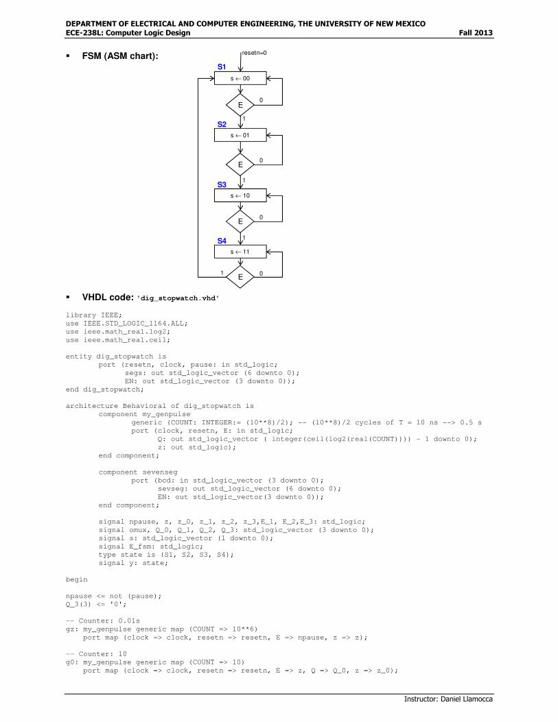
� FSM (ASM chart): � VHDL code: 'dig_stopwatch.vhd'
library IEEE;
use IEEE.STD_LOGIC_1164.ALL;
use ieee.math_real.log2;
use ieee.math_real.ceil;
entity dig_stopwatch is
port (resetn, clock, pause: in std_logic;
segs: out std_logic_vector (6 downto 0);
EN: out std_logic_vector (3 downto 0));
end dig_stopwatch;
architecture Behavioral of dig_stopwatch is
component my_genpulse
generic (COUNT: INTEGER:= (10**8)/2); -- (10**8)/2 cycles of T = 10 ns --> 0.5 s
port (clock, resetn, E: in std_logic;
Q: out std_logic_vector ( integer(ceil(log2(real(COUNT)))) - 1 downto 0);
z: out std_logic);
end component;
component sevenseg
port (bcd: in std_logic_vector (3 downto 0);
sevseg: out std_logic_vector (6 downto 0);
EN: out std_logic_vector(3 downto 0));
end component;
signal npause, z, z_0, z_1, z_2, z_3,E_1, E_2,E_3: std_logic;
signal omux, Q_0, Q_1, Q_2, Q_3: std_logic_vector (3 downto 0);
signal s: std_logic_vector (1 downto 0);
signal E_fsm: std_logic;
type state is (S1, S2, S3, S4);
signal y: state;
begin
npause <= not (pause);
Q_3(3) <= '0';
-- Counter: 0.01s
gz: my_genpulse generic map (COUNT => 10**6)
port map (clock => clock, resetn => resetn, E => npause, z => z);
-- Counter: 10
g0: my_genpulse generic map (COUNT => 10)
port map (clock => clock, resetn => resetn, E => z, Q => Q_0, z => z_0);
1
S1
resetn=0
s ← 00
s ← 01
S2
s ← 10
S3
s ← 11
S4
E
E
E
E
1
1
1
0
0
0
0

DEPARTMENT OF ELECTRICAL AND COMPUTER ENGINEERING, THE UNIVERSITY OF NEW MEXICO
ECE-238L: Computer Logic Design Fall 2013
Instructor: Daniel Llamocca
-- Counter: 10
g1: my_genpulse generic map (COUNT => 10)
port map (clock => clock, resetn => resetn, E => E_1, Q => Q_1, z => z_1);
E_1 <= z and z_0;
-- Counter: 10
g2: my_genpulse generic map (COUNT => 10)
port map (clock => clock, resetn => resetn, E => E_2, Q => Q_2, z => z_2);
E_2 <= E_1 and z_1;
-- Counter: 6
g3: my_genpulse generic map (COUNT => 6)
port map (clock => clock, resetn => resetn, E => E_3, Q => Q_3 (2 downto 0),z => z_3);
E_3 <= E_2 and z_2;
-- Multiplexor
with s select
omux <= Q_0 when "00",
Q_1 when "01",
Q_2 when "10",
Q_3 when others;
seg7: sevenseg port map (bcd => omux, sevseg => segs);
-- 2-to-4 decoder
with s select
EN <= "1110" when "00",
"1101" when "01",
"1011" when "10",
"0111" when "11",
"1111" when others;
-- Counter: 0.001s
gfsm: my_genpulse generic map (COUNT => 10**5)
port map (clock => clock, resetn => resetn, E => '1', z => E_fsm);
Transitions: process (resetn, clock, E_fsm)
begin
if resetn = '0' then -- asynchronous signal
y <= S1; -- if resetn asserted, go to initial state: S1
elsif (clock'event and clock = '1') then
if E_fsm = '1' then
case y is
when S1 => y <= S2;
when S2 => y <= S3;
when S3 => y <= S4;
when S4 => y <= S1;
end case;
end if;
end if;
end process;
Outputs: process (y)
begin
case y is
when S1 => s <= "00";
when S2 => s <= "01";
when S3 => s <= "10";
when S4 => s <= "11";
end case;
end process;
end Behavioral;
DEPARTMENT OF ELECTRICAL AND COMPUTER ENGINEERING, THE UNIVERSITY OF NEW MEXICO
ECE-238L: Computer Logic Design Fall 2013
Instructor: Daniel Llamocca
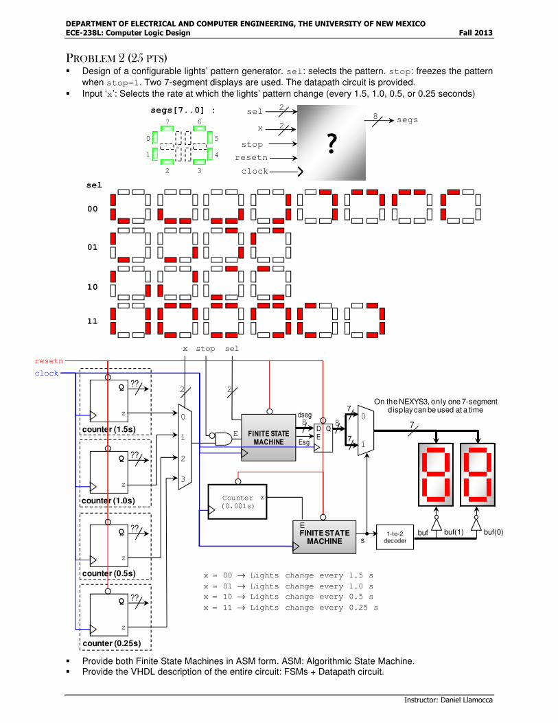
PROBLEM 2 (25 PTS) � Design of a configurable lights’ pattern generator. sel: selects the pattern. stop: freezes the pattern
when stop=1. Two 7-segment displays are used. The datapath circuit is provided.
� Input ‘x’: Selects the rate at which the lights’ pattern change (every 1.5, 1.0, 0.5, or 0.25 seconds)
� Provide both Finite State Machines in ASM form. ASM: Algorithmic State Machine. � Provide the VHDL description of the entire circuit: FSMs + Datapath circuit.
sel
00
01
10
11
segs[7..0] :
?clock
resetn
28 segs
2
sel
x
stop
7 6
5
4
0
1
2 3
FINITE STATEMACHINE
resetn
Q
clock
??
counter (1.5s)
z
Q ??
counter (1.0s)
z
Q ??
counter (0.5s)
z
FINITE STATE
MACHINE
stop
8
Q ??
counter (0.25s)
z
0
1
2
3
x
2
E
70
1
1-to-2decoder
7
buf buf(1) buf(0)
sel
2
s
x = 00 → Lights change every 1.5 s
x = 01 → Lights change every 1.0 s
x = 10 → Lights change every 0.5 s
x = 11 → Lights change every 0.25 s
On the NEXYS3, only one 7-segmentdisplay can be used at a time
Counter
(0.001s)
z
E
D QE
dseg
7Esg
8

DEPARTMENT OF ELECTRICAL AND COMPUTER ENGINEERING, THE UNIVERSITY OF NEW MEXICO
ECE-238L: Computer Logic Design Fall 2013
Instructor: Daniel Llamocca
� Main FSM (ASM chart):
S1resetn=0
1
0E
sel
S2a
1
0E
S3a
1
0E
S4a
1
0E
S2b
1
0E
S3b
1
0E
S4b
1
0E
S2c
1
0E
S3c
1
0E
S4c
1
0E
S2d
1
0E
S3d
1
0E
S4d
1
0E
00 11
01 10
dseg←00000111, Esg←1 dseg←00000101, Esg←1 dseg←00010001, Esg←1 dseg←00110011, Esg←1
dseg←00001110, Esg←1 dseg←00010100, Esg←1 dseg←00100010, Esg←1 dseg←11100111, Esg←1
dseg←00011100, Esg←1 dseg←01010000, Esg←1 dseg←01000100, Esg←1 dseg←11001100, Esg←1
dseg←00111000, Esg←1 dseg←01000001, Esg←1 dseg←10001000, Esg←1 dseg←11111001, Esg←1
S5a
1 0
Edseg←01110000, Esg←1
S6a
10E dseg←11100000, Esg←1
S7a
1 0
Edseg←11000001, Esg←1
S5d
1
0
E
S6d
1
0
E
dseg←10000111, Esg←1
dseg←01111000, Esg←1S8a
1
0
E
dseg←10000011, Esg←1
DEPARTMENT OF ELECTRICAL AND COMPUTER ENGINEERING, THE UNIVERSITY OF NEW MEXICO
ECE-238L: Computer Logic Design Fall 2013
Instructor: Daniel Llamocca
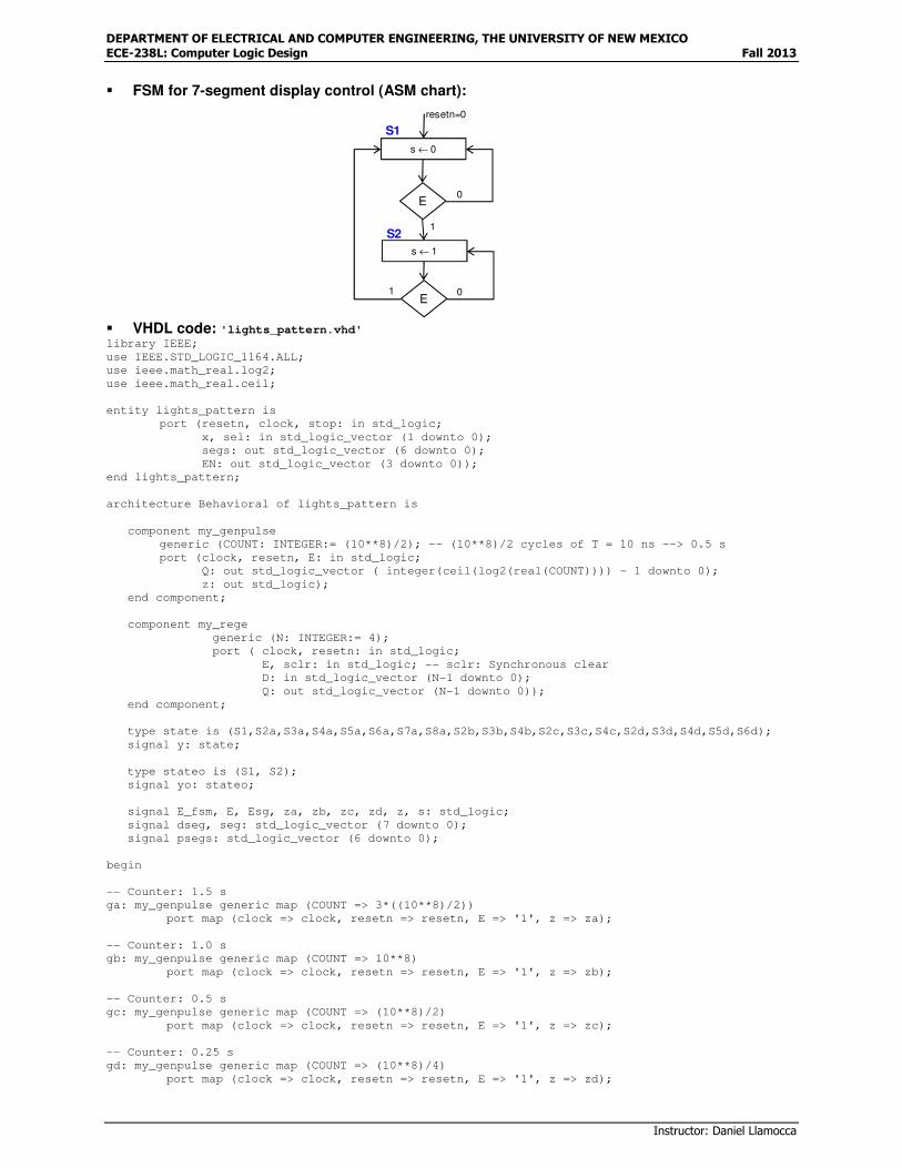
� FSM for 7-segment display control (ASM chart): � VHDL code: 'lights_pattern.vhd' library IEEE;
use IEEE.STD_LOGIC_1164.ALL;
use ieee.math_real.log2;
use ieee.math_real.ceil;
entity lights_pattern is
port (resetn, clock, stop: in std_logic;
x, sel: in std_logic_vector (1 downto 0);
segs: out std_logic_vector (6 downto 0);
EN: out std_logic_vector (3 downto 0));
end lights_pattern;
architecture Behavioral of lights_pattern is
component my_genpulse
generic (COUNT: INTEGER:= (10**8)/2); -- (10**8)/2 cycles of T = 10 ns --> 0.5 s
port (clock, resetn, E: in std_logic;
Q: out std_logic_vector ( integer(ceil(log2(real(COUNT)))) - 1 downto 0);
z: out std_logic);
end component;
component my_rege
generic (N: INTEGER:= 4);
port ( clock, resetn: in std_logic;
E, sclr: in std_logic; -- sclr: Synchronous clear
D: in std_logic_vector (N-1 downto 0);
Q: out std_logic_vector (N-1 downto 0));
end component;
type state is (S1,S2a,S3a,S4a,S5a,S6a,S7a,S8a,S2b,S3b,S4b,S2c,S3c,S4c,S2d,S3d,S4d,S5d,S6d);
signal y: state;
type stateo is (S1, S2);
signal yo: stateo;
signal E_fsm, E, Esg, za, zb, zc, zd, z, s: std_logic;
signal dseg, seg: std_logic_vector (7 downto 0);
signal psegs: std_logic_vector (6 downto 0);
begin
-- Counter: 1.5 s
ga: my_genpulse generic map (COUNT => 3*((10**8)/2))
port map (clock => clock, resetn => resetn, E => '1', z => za);
-- Counter: 1.0 s
gb: my_genpulse generic map (COUNT => 10**8)
port map (clock => clock, resetn => resetn, E => '1', z => zb);
-- Counter: 0.5 s
gc: my_genpulse generic map (COUNT => (10**8)/2)
port map (clock => clock, resetn => resetn, E => '1', z => zc);
-- Counter: 0.25 s
gd: my_genpulse generic map (COUNT => (10**8)/4)
port map (clock => clock, resetn => resetn, E => '1', z => zd);
S1
resetn=0
s ← 0
s ← 1
S2
E
E
0
0
1
1

DEPARTMENT OF ELECTRICAL AND COMPUTER ENGINEERING, THE UNIVERSITY OF NEW MEXICO
ECE-238L: Computer Logic Design Fall 2013
Instructor: Daniel Llamocca
-- Multiplexor for the counter outputs:
with x select
z <= za when "00",
zb when "01",
zc when "10",
zd when others;
E <= z and not(stop);
-- 8-bit register
rP: my_rege generic map (N => 8)
port map (clock => clock, resetn => resetn, E => Esg, sclr => '0', D => dseg, Q => seg);
-- Multiplexor for the 7-segment displays:
with s select
psegs <= seg(6 downto 3)&"000" when '0',
seg(7)&"00"&seg(2 downto 0)&'0' when others;
-- segs: |a|b|c|d|e|f|g|
segs <= not(psegs); -- Active-low outputs
-- Counter: 0.001 s
gfsm: my_genpulse generic map (COUNT => 10**5)
port map (clock => clock, resetn => resetn, E => '1', z => E_fsm);
-- 1-to-2 decoder
with s select
EN <= "1011" when '0',
"0111" when others;
-- Main FSM:
Transitions: process (resetn, clock, E, sel)
begin
if resetn = '0' then -- asynchronous signal
y <= S1; -- if resetn asserted, go to initial state: S1
elsif (clock'event and clock = '1') then
case y is
when S1 =>
if E = '1' then
case sel is
when "00" => y <= S2a;
when "01" => y <= S2b;
when "10" => y <= S2c;
when others => y <= S2d;
end case;
else
y <= S1;
end if;
when S2a => if E = '1' then y <= S3a; else y <= S2a; end if;
when S3a => if E = '1' then y <= S4a; else y <= S3a; end if;
when S4a => if E = '1' then y <= S5a; else y <= S4a; end if;
when S5a => if E = '1' then y <= S6a; else y <= S5a; end if;
when S6a => if E = '1' then y <= S7a; else y <= S6a; end if;
when S7a => if E = '1' then y <= S8a; else y <= S7a; end if;
when S8a => if E = '1' then y <= S1; else y <= S8a; end if;
when S2b => if E = '1' then y <= S3b; else y <= S2b; end if;
when S3b => if E = '1' then y <= S4b; else y <= S3b; end if;
when S4b => if E = '1' then y <= S1; else y <= S4b; end if;
when S2c => if E = '1' then y <= S3c; else y <= S2c; end if;
when S3c => if E = '1' then y <= S4c; else y <= S3c; end if;
when S4c => if E = '1' then y <= S1; else y <= S4c; end if;
when S2d => if E = '1' then y <= S3d; else y <= S2d; end if;
when S3d => if E = '1' then y <= S4d; else y <= S3d; end if;
when S4d => if E = '1' then y <= S5d; else y <= S4d; end if;
when S5d => if E = '1' then y <= S6d; else y <= S5d; end if;
when S6d => if E = '1' then y <= S1; else y <= S6d; end if;
end case;
end if;
end process;

DEPARTMENT OF ELECTRICAL AND COMPUTER ENGINEERING, THE UNIVERSITY OF NEW MEXICO
ECE-238L: Computer Logic Design Fall 2013
Instructor: Daniel Llamocca
Outputs: process (y, E, sel)
begin
-- Initialization of FSM outputs:
dseg <= (others => '0'); Esg <= '0';
case y is
when S1 =>
if E = '1' then
case sel is
when "00" => dseg <= "00000111"; Esg <= '1';
when "01" => dseg <= "00000101"; Esg <= '1';
when "10" => dseg <= "00010001"; Esg <= '1';
when others => dseg <= "00110011"; Esg <= '1';
end case;
end if;
when S2a => if E = '1' then dseg <= "00001110"; Esg <= '1'; end if;
when S3a => if E = '1' then dseg <= "00011100"; Esg <= '1'; end if;
when S4a => if E = '1' then dseg <= "00111000"; Esg <= '1'; end if;
when S5a => if E = '1' then dseg <= "01110000"; Esg <= '1'; end if;
when S6a => if E = '1' then dseg <= "11100000"; Esg <= '1'; end if;
when S7a => if E = '1' then dseg <= "11000001"; Esg <= '1'; end if;
when S8a => if E = '1' then dseg <= "10000011"; Esg <= '1'; end if;
when S2b => if E = '1' then dseg <= "00010100"; Esg <= '1'; end if;
when S3b => if E = '1' then dseg <= "01010000"; Esg <= '1'; end if;
when S4b => if E = '1' then dseg <= "01000001"; Esg <= '1'; end if;
when S2c => if E = '1' then dseg <= "00100010"; Esg <= '1'; end if;
when S3c => if E = '1' then dseg <= "01000100"; Esg <= '1'; end if;
when S4c => if E = '1' then dseg <= "10001000"; Esg <= '1'; end if;
when S2d => if E = '1' then dseg <= "11100111"; Esg <= '1'; end if;
when S3d => if E = '1' then dseg <= "11001100"; Esg <= '1'; end if;
when S4d => if E = '1' then dseg <= "11111001"; Esg <= '1'; end if;
when S5d => if E = '1' then dseg <= "10000111"; Esg <= '1'; end if;
when S6d => if E = '1' then dseg <= "01111000"; Esg <= '1'; end if;
end case;
end process;
-- FSM: serializer for the 7-segment display
Trans: process (resetn, clock, E_fsm)
begin
if resetn = '0' then -- asynchronous signal
yo <= S1; -- if resetn asserted, go to initial state: S1
elsif (clock'event and clock = '1') then
if E_fsm = '1' then
case yo is
when S1 => yo <= S2;
when S2 => yo <= S1;
end case;
end if;
end if;
end process;
Outps: process (yo)
begin
case yo is
when S1 => s <= '0';
when S2 => s <= '1';
end case;
end process;
end Behavioral;

DEPARTMENT OF ELECTRICAL AND COMPUTER ENGINEERING, THE UNIVERSITY OF NEW MEXICO
ECE-238L: Computer Logic Design Fall 2013
Instructor: Daniel Llamocca
PROBLEM 3 (20 PTS) � The figure depicts the architecture of a simple processor.
� Register G: Parallel Access left-shift register with enable. s_l = 1 → Load, s_l = 0 → Left-shift
� The figure below depicts the datapath and the FSM of the Control Circuit:
R0E
O_R0
E_R0
R1E
O_R1
E_R1
R2E
O_R2
E_R2
R3E
O_R3
E_R3
AE
O_G
E_A
GE
s_l
ALU
E_ext
CONTROL CIRCUIT
Data
op
4
w
fun7
done
BUS
B
E_G
QDn
Data_inn
din0
L_G
left-shift
Rx1
Rx0
Ex
DECODER
with
enable
0
1
2
3
0
1
E
E_R0
E_R1
E_R2
E_R3
Ry
Eo
DECODER
with
enable
0
1
2
3
0
1
E
O_R0
O_R1
O_R2
O_R3
Rx
so
0
1
2
22
FSMdone
w
f3
Ex Eo so E_G
O_G
E_ext
op
4E_fun
QD
E
7fun
7funq
funq = |f2|f1|f0|Ry1|Ry0|Rx1|Rx0|
E_A
L_G
E_fun

DEPARTMENT OF ELECTRICAL AND COMPUTER ENGINEERING, THE UNIVERSITY OF NEW MEXICO
ECE-238L: Computer Logic Design Fall 2013
Instructor: Daniel Llamocca
� The following table specifies the behavior of the Arithmetic-Logic Unit (ALU). This ALU is purely combinatorial.
op Operation Function Unit
0000
0001
0010
0011
0100
0101
0110
0111
y <= A
y <= A + 1
y <= A - 1
y <= B
y <= B + 1
y <= B – 1
y <= A + B
y <= A – B
Transfer ‘A’
Increment ‘A’
Decrement ‘A’
Transfer ‘B’
Increment ‘B’
Decrement ‘B’
Add ‘A’ and ‘B’
Subtract ‘B’ from 'A'
Arithmetic
1000
1001
1010
1011
1100
1101
1110
1111
y <= not A
y <= not B
y <= A AND B
y <= A OR B
y <= A NAND B
y <= A NOR B
y <= A XOR B
y <= A XNOR B
Complement ‘A’
Complement ‘B’
AND
OR
NAND
NOR
XOR
XNOR
Logic
� Operation: Every time w = '1', we store the input ���, then proceed to execute it. � The 7 bits of the stored input, called ����, are arranged as: ���� = |��|��|� |���|�� |���|�� |. The
first 3 bits specify the operation, while the other 4 bits specify the registers over which the operations are applied.
f Operation Function
000 Load Rx, Data Rx ← Data
001 Add Rx, Data Rx ← Rx + Data
010 Not Rx Rx ← NOT (Rx)
011 Sub Rx, Ry Rx ← Rx - Ry
100 Add Rx, Ry Rx ← Rx + Ry
101 Move Rx, Ry Rx ← Ry
110 sla Rx Rx ← left-shift Rx
111 Addi Rx, 2 Rx ← Rx + 2
� Design the Finite State Machine (provide it in ASM form) that can issue the correct set of signals for
all the listed operations.

DEPARTMENT OF ELECTRICAL AND COMPUTER ENGINEERING, THE UNIVERSITY OF NEW MEXICO
ECE-238L: Computer Logic Design Fall 2013
Instructor: Daniel Llamocca
� FSM (ASM chart):
PROBLEM 4 (10 PTS) � For the following error-detection system, provide the truth table and sketch the circuits of i) the Odd
Parity Generator, and ii) Odd parity checker.
� Odd parity generator: TPB is such that |A|B|C|TPB| has an odd number of bits. � Odd parity checker: Checks whether |A|B|C|TPB| has an odd number of bits. If this is the case, RPB
= '0', otherwise RPB = '1' (signaling an error).
Odd Parity
Generator
Odd Parity
Checker
A
B
C
A
B
C
RPBTPB
Transmitted bits
S1
S2
resetn=0
1
0
E_ext, Ex ← 1
done ← 1
Eo, Ex ← 1
done ← 1
000
101
Eo, so ← 1
E_A ← 1
Eo ← 1
E_G,L_G ← 1
op ← 0110
O_G, Ex ← 1
done ← 1
100
S6a
S6b
Eo ← 1
E_G,L_G ← 1
op ← 0111
O_G, Ex ← 1
done ← 1
S5a
S5b
Eo, so ← 1
E_A ← 1
O_G, Ex ← 1
done ← 1
S4a
Eo, so ← 1
E_G,L_G ← 1
op ← 1001
E_ext ← 1
E_G,L_G ← 1
op ← 0110
O_G, Ex ← 1
done ← 1
S3a
S3b
Eo, so ← 1
E_A ← 1
E_G ← 1
L_G ← 0
O_G, Ex ← 1
done ← 1
S7a
S7b
Eo, so ← 1
E_G,L_G ← 1
op ← 0011
E_G,L_G ← 1
O_G ← 1
op ← 0100
O_G, Ex ← 1
done ← 1
S8a
S8b
Eo, so ← 1
E_G,L_G ← 1
op ← 0100
w
f
E_fun ← 1
011
010001
110
111

DEPARTMENT OF ELECTRICAL AND COMPUTER ENGINEERING, THE UNIVERSITY OF NEW MEXICO
ECE-238L: Computer Logic Design Fall 2013
Instructor: Daniel Llamocca
� Sketch the schematics of an n-bit comparator of two numbers represented in 2’s complement.
Required outputs: AgeB, AlB, AeB. If A >= B → AgeB = 1. If A < B → AlB = 1. If A = B
→ AeB = 1. You can use adders (specify the number of bits) and XOR gates.
Make sure that your circuit works in all circumstances (consider that A and B may cause overflow, you need to avoid it).
TPB
1
0
0
1
0
1
1
0
0 0 0
0 0 1
0 1 0
0 1 1
1 0 0
1 0 1
1 1 0
1 1 1
A B C RPB
1
0
0
1
0
1
1
0
0
1
1
0
1
0
0
1
0 0 0 0
0 0 0 1
0 0 1 0
0 0 1 1
0 1 0 0
0 1 0 1
0 1 1 0
0 1 1 1
1 0 0 0
1 0 0 1
1 0 1 0
1 0 1 1
1 1 0 0
1 1 0 1
1 1 1 0
1 1 1 1
A B C TPB
A
B
C
TPB
A
B
C
TPB
RPB
Odd Parity Generator Odd Parity Checker
AeB
cn-1FA
A0 B0
c0
s0
FA
A1 B1
c1
s1
FA
A2 B2
c2
s2
c3FA
An-1 Bn-1
sn
cncout cin
1
...
sn = 0 → A-B ≥ 0
sn = 1 → A-B < 0
AlB AgeB
...
...
cn-2FA
An-1 Bn-1
sn-1
A
B
n
n
An-1
Bn-1
n+1
n+1

DEPARTMENT OF ELECTRICAL AND COMPUTER ENGINEERING, THE UNIVERSITY OF NEW MEXICO
ECE-238L: Computer Logic Design Fall 2013
Instructor: Daniel Llamocca
PROBLEM 5 (25 PTS) � LUT connected to a bidirectional port: An LUT4-to-1 (also called LUT4) can implement a 4-input
function. The VHDL code is provided below. Note that the values stored in the LUT are constant, hence those values are entered as a parameter in the VHDL code:
library IEEE;
use IEEE.STD_LOGIC_1164.ALL;
entity my4to1LUT is
generic (data: std_logic_vector(15 downto 0):=x"FEAB"); -- LUT 4-to-1 contents
port ( ILUT: in std_logic_vector (3 downto 0);
OLUT: out std_logic);
end my4to1LUT;
architecture Behavioral of my4to1LUT is
begin
with ILUT select
OLUT <= data(0) when "0000",
data(1) when "0001",
data(2) when "0010",
data(3) when "0011",
data(4) when "0100",
data(5) when "0101",
data(6) when "0110",
data(7) when "0111",
data(8) when "1000",
data(9) when "1001",
data(10) when "1010",
data(11) when "1011",
data(12) when "1100",
data(13) when "1101",
data(14) when "1110",
data(15) when "1111",
'0' when others;
end Behavioral;
� LUTs with more than four inputs can be built by grouping several LUT 4-to-1 and MUXs. The figure
below shows how an LUT 6-to-1 can be built. � An LUT with more than one output can also be built. The figure below show how we can create an
LUT 6-to-6 (we just use six LUT 6-to-1). You are asked to design a system with an LUT 6-to-6. This will be accomplished in a series of steps: � Provide the VHDL code of an LUT 6-to-1. You can built it by i) grouping four LUT4-to-1 and MUXs, or
ii) using only one VHDL file (similar to my4to1LUT.vhd). The entity should look like this:
entity my6to1LUT is
generic (data: std_logic_vector(63 downto 0):=x"FEAB97CA003E19CC"); -- 64 values
port ( ILUT: in std_logic_vector (5 downto 0);
OLUT: out std_logic);
end my6to1LUT;
ILUT4 OLUT
4-to-1
Look-up Table
address
(Read-only memory
with 16 positions)
data(0)
data(1)
data(2)
data(3)
data(4)
data(5)
data(6)
data(7)
data(8)
data(9)
data(10)
data(11)
data(12)
data(13)
data(14)
data(15)
6
4 4 4 4
2 M
SB
s
4 LSBs
LUT5-to-1
LUT6-to-1
LUT6 to 1
LUT6 to 1
LUT6 to 1
6
6
6
6
b0
b4
b5
b5 b1 b0
≡
6
LUT 6-to-6
6 bits
64 w
ord
s o
f 6 b
its
LUT 6-to-6
LUT
4
LUT
4
LUT
4
LUT
4
MUX MUX
MUX
...
...
...
LI
LI(4)
LI(5)
LI(3..0)
co
lum
n 5
co
lum
n 1
co
lum
n 0
66

DEPARTMENT OF ELECTRICAL AND COMPUTER ENGINEERING, THE UNIVERSITY OF NEW MEXICO
ECE-238L: Computer Logic Design Fall 2013
Instructor: Daniel Llamocca
� Write the VHDL code for an LUT 6-to-6. You must built it by grouping six LUT 6-to-1. The entity should look like this:
entity my6to6LUT is
generic (data5: std_logic_vector(63 downto 0):=x"FEAB97CA003E19CC"; -- column 5
data4: std_logic_vector(63 downto 0):=x"AABBCCFFEE99098A"; -- column 4
data3: std_logic_vector(63 downto 0):=x"E595BEBECAFEDADA"; -- column 3
data2: std_logic_vector(63 downto 0):=x"FACE09093E3EECAB"; -- column 2
data1: std_logic_vector(63 downto 0):=x"DECAFFFF09EA3200"; -- column 1
data0: std_logic_vector(63 downto 0):=x"ACADE412BAFE125E"); -- column 0
port ( ILUT: in std_logic_vector (5 downto 0);
OLUT: out std_logic_vector (5 downto 0));
end my6to6LUT; Important: When instantiating the my6to1LUT component, we use the port map instruction to make
interconnections. Now, we also need to provide the correct parameter to each my6to1LUT
component. This is done usually the generic map instruction.
� Final System: Provide the VHDL code of the circuit depicted below. Use the Structural Description
by interconnecting the following components: i) LUT 6-to-6, ii) 6-bit register, and iii) Tri-state buffers. Important: The port 'DATA' can be input or output at different times. Use INOUT in your VHDL code.
� LUT6-to-6 contents: We want this LUT 6-to-6 to provide the following function: ���� = ����� .��� Example: ���� = 35�010011�� → ���� = �35
.��� = 30�011110�� Compute the contents of the LUT 6-to-6 and provide each column in hexadecimal format as:
data5, data4, data3, data2, data1, data0 (generic input parameters)
� Complete the Timing diagram shown below. Note that the port DATA is input at some times, and output at other times.
100111
LUT6-to-6
6 6
OE
clk
resetn
DATA
OE
110001
DI DODATA
6
DI
DO
D Q
clk
resetn
6
E
000111 100001
110001

DEPARTMENT OF ELECTRICAL AND COMPUTER ENGINEERING, THE UNIVERSITY OF NEW MEXICO
ECE-238L: Computer Logic Design Fall 2013
Instructor: Daniel Llamocca
� LUT6-to-6 contents: � VHDL code: 'sysLUT6to6.vhd' library IEEE;
use IEEE.STD_LOGIC_1164.ALL;
entity sysLUT6to6 is
generic (data5: std_logic_vector(63 downto 0):=x"ffffffc000000000"; -- column 5
data4: std_logic_vector(63 downto 0):=x"fc00003ffffc0000"; -- column 4
data3: std_logic_vector(63 downto 0):=x"03ff003ff003ff00"; -- column 3
data2: std_logic_vector(63 downto 0):=x"83e0f83e0f83e0f0"; -- column 2
data1: std_logic_vector(63 downto 0):=x"639ce739ce7398cc"; -- column 1
data0: std_logic_vector(63 downto 0):=x"5a5296b5ad6a56aa"); -- column 0
port (clk, resetn, OE: in std_logic;
data: inout std_logic_vector (5 downto 0));
end sysLUT6to6;
architecture structure of sysLUT6to6 is
component my_rege
generic (N: INTEGER:= 4);
port ( clock, resetn: in std_logic;
E, sclr: in std_logic; -- sclr: Synchronous clear
D: in std_logic_vector (N-1 downto 0);
Q: out std_logic_vector (N-1 downto 0));
end component;
component my6to6LUT
generic (data5: std_logic_vector(63 downto 0):=x"FEAB97CA003E19CC"; -- column 5
data4: std_logic_vector(63 downto 0):=x"AABBCCFFEE99098A"; -- column 4
data3: std_logic_vector(63 downto 0):=x"E595BEBECAFEDADA"; -- column 3
data2: std_logic_vector(63 downto 0):=x"FACE09093E3EECAB"; -- column 2
data1: std_logic_vector(63 downto 0):=x"DECAFFFF09EA3200"; -- column 1
data0: std_logic_vector(63 downto 0):=x"ACADE412BAFE125E"); -- column 0
port ( ILUT: in std_logic_vector (5 downto 0);
OLUT: out std_logic_vector (5 downto 0));
end component;
signal DI, DO, QR: std_logic_vector (5 downto 0);
begin
ri: my_rege generic map (N => 6)
port map (clock => clk, resetn => resetn, E => OE, sclr => '0', D => DI, Q => QR);
LUT6to6: my6to6LUT generic map (data5 => data5, data4 => data4, data3 => data3, data2 => data2,
data1 => data1, data0 => data0)
port map (ILUT => QR, OLUT => DO);
DATA <= DO when OE = '0' else (others => 'Z');
DI <= DATA when OE = '1' else (others => 'Z');
end structure;
LUT 6-to-6:
63
0 0 0 0 C A
0 0 0 F C A
0 0 F 0 8 6
0 0 F E 9 5
0 C 3 3 3 A
0 F 0 8 7 6
0 F 0 F E D
0 F F 0 C A
0 F F E 9 5
C 3 3 3 3 B
F 0 0 8 7 6
F 0 0 F E 9
F 0 F 0 C 2
F 0 F E 9 5
F C 3 3 3 A
F F 0 8 6 5
hexadecimals converted
in this direction
b5 b4 b3 b2 b1 b0
data5
data4
data3
data2
data1
data0
0
...

DEPARTMENT OF ELECTRICAL AND COMPUTER ENGINEERING, THE UNIVERSITY OF NEW MEXICO
ECE-238L: Computer Logic Design Fall 2013
Instructor: Daniel Llamocca
� VHDL code: 'my6to6LUT' library IEEE;
use IEEE.STD_LOGIC_1164.ALL;
entity my6to6LUT is
generic (data5: std_logic_vector(63 downto 0):=x"FEAB97CA003E19CC"; -- column 5
data4: std_logic_vector(63 downto 0):=x"AABBCCFFEE99098A"; -- column 4
data3: std_logic_vector(63 downto 0):=x"E595BEBECAFEDADA"; -- column 3
data2: std_logic_vector(63 downto 0):=x"FACE09093E3EECAB"; -- column 2
data1: std_logic_vector(63 downto 0):=x"DECAFFFF09EA3200"; -- column 1
data0: std_logic_vector(63 downto 0):=x"ACADE412BAFE125E"); -- column 0
port ( ILUT: in std_logic_vector (5 downto 0);
OLUT: out std_logic_vector (5 downto 0));
end my6to6LUT;
architecture Behavioral of my6to6LUT is
component my6to1LUT
generic (data: std_logic_vector(63 downto 0):=x"ACCABEBEFACEFEAB");
port ( ILUT: in std_logic_vector (5 downto 0);
OLUT: out std_logic);
end component;
signal OLUT_l, OLUT_h: std_logic;
begin
-- 6-to-1 LUT holding contents of column 5:
r5: my6to1LUT generic map (data => data5)
port map (ILUT => ILUT, OLUT => OLUT(5));
-- 6-to-1 LUT holding contents of column 4:
r4: my6to1LUT generic map (data => data4)
port map (ILUT => ILUT, OLUT => OLUT(4));
-- 6-to-1 LUT holding contents of column 3:
r3: my6to1LUT generic map (data => data3)
port map (ILUT => ILUT, OLUT => OLUT(3));
-- 6-to-1 LUT holding contents of column 2:
r2: my6to1LUT generic map (data => data2)
port map (ILUT => ILUT, OLUT => OLUT(2));
-- 6-to-1 LUT holding contents of column 1:
r1: my6to1LUT generic map (data => data1)
port map (ILUT => ILUT, OLUT => OLUT(1));
-- 6-to-1 LUT holding contents of column 0:
r0: my6to1LUT generic map (data => data0)
port map (ILUT => ILUT, OLUT => OLUT(0));
end Behavioral;
� VHDL code: 'my6to1LUT' library IEEE;
use IEEE.STD_LOGIC_1164.ALL;
entity my6to1LUT is
generic (data: std_logic_vector(63 downto 0):=x"ACCABEBEFACEFEAB");
port ( ILUT: in std_logic_vector (5 downto 0);
OLUT: out std_logic);
end my6to1LUT;
architecture Behavioral of my6to1LUT is
component my5to1LUT
generic (data: std_logic_vector(31 downto 0):=x"FACEFEAB");
port ( ILUT: in std_logic_vector (4 downto 0);
OLUT: out std_logic);
end component;
signal OLUT_l, OLUT_h: std_logic;
begin
-- 5-to-1 LUT holding contents: data(31 downto 0)
rl: my5to1LUT generic map (data => data(31 downto 0))
port map (ILUT => ILUT(4 downto 0), OLUT => OLUT_l);
-- 5-to-1 LUT holding contents: data(63 downto 32)
rh: my5to1LUT generic map (data => data (63 downto 32))
port map (ILUT => ILUT(4 downto 0), OLUT => OLUT_h);
with ILUT(5) select
OLUT <= OLUT_l when '0',
OLUT_h when others;
end Behavioral;

DEPARTMENT OF ELECTRICAL AND COMPUTER ENGINEERING, THE UNIVERSITY OF NEW MEXICO
ECE-238L: Computer Logic Design Fall 2013
Instructor: Daniel Llamocca
� VHDL code: 'my5to1LUT' library IEEE;
use IEEE.STD_LOGIC_1164.ALL;
entity my5to1LUT is
generic (data: std_logic_vector(31 downto 0):=x"FACEFEAB");
port ( ILUT: in std_logic_vector (4 downto 0);
OLUT: out std_logic);
end my5to1LUT;
architecture Behavioral of my5to1LUT is
component my4to1LUT
generic (data: std_logic_vector(15 downto 0):=x"FEAB");
port ( ILUT: in std_logic_vector (3 downto 0);
OLUT: out std_logic);
end component;
signal OLUT_l, OLUT_h: std_logic;
begin
-- 4-to-1 LUT holding contents: data(15 downto 0)
rl: my4to1LUT generic map (data => data(15 downto 0))
port map (ILUT => ILUT(3 downto 0), OLUT => OLUT_l);
-- 4-to-1 LUT holding contents: data(31 downto 16)
rh: my4to1LUT generic map (data => data (31 downto 16))
port map (ILUT => ILUT(3 downto 0), OLUT => OLUT_h);
with ILUT(4) select
OLUT <= OLUT_l when '0',
OLUT_h when others;
end Behavioral;
� VHDL Testbench LIBRARY ieee;
USE ieee.std_logic_1164.ALL;
use ieee.std_logic_arith.all;
ENTITY tb_sysLUT6to6 IS
END tb_sysLUT6to6;
ARCHITECTURE behavior OF tb_sysLUT6to6 IS
-- Component Declaration for the Unit Under Test (UUT)
COMPONENT sysLUT6to6
PORT (clk : IN std_logic;
resetn : IN std_logic;
OE : IN std_logic;
data : INOUT std_logic_vector(5 downto 0));
END COMPONENT;
--Inputs
signal clk : std_logic := '0';
signal resetn : std_logic := '0';
signal OE : std_logic := '0';
--BiDirs
signal data : std_logic_vector(5 downto 0);
-- Clock period definitions
constant clk_period : time := 10 ns;
BEGIN
-- Instantiate the Unit Under Test (UUT)
uut: sysLUT6to6 PORT MAP (clk => clk, resetn => resetn, OE => OE, data => data);
-- Clock process definitions
clk_process :process
begin
clk <= '0';
wait for clk_period/2;
clk <= '1';
wait for clk_period/2;
end process;

DEPARTMENT OF ELECTRICAL AND COMPUTER ENGINEERING, THE UNIVERSITY OF NEW MEXICO
ECE-238L: Computer Logic Design Fall 2013
Instructor: Daniel Llamocca
-- Stimulus process
stim_proc: process
begin
-- hold reset state for 100 ns.
resetn <= '0'; DATA <= "ZZZZZZ"; wait for 100 ns;
resetn <= '1'; wait for clk_period;
OE <= '1'; DATA <= "110001"; wait for 2*clk_period;
OE <= '0'; DATA <= "ZZZZZZ"; wait for 2*clk_period;
OE <= '1'; DATA <= "100111"; wait for 2*clk_period;
OE <= '0'; DATA <= "ZZZZZZ"; wait for 2*clk_period;
OE <= '1'; DATA <= "000111"; wait for 2*clk_period;
OE <= '0'; DATA <= "ZZZZZZ"; wait for 2*clk_period;
OE <= '1'; DATA <= "100001"; wait for 2*clk_period;
OE <= '0'; DATA <= "ZZZZZZ"; wait for 2*clk_period;
wait for 4*clk_period;
OE <= '1';
lp: for i in 0 to 63 loop
DATA <= conv_std_logic_vector(i,6); wait for clk_period;
end loop;
end process;
END;
� Timing diagram:
EXTRA CREDIT (+10 PTS) � Demonstrate the circuits of Problems 1 and 2 working on the NEXYS3 board. � UCF File for Problem 1: 'dig_stopwatch.ucf'
# Inputs
NET "clock" LOC = "V10";
NET "resetn" LOC = "T10"; #SW0
NET "pause" LOC = "T9"; #SW1
# Outputs
NET "EN<3>" LOC = "P17"; # anode (1st display from left to right)
NET "EN<2>" LOC = "P18"; # anode (2nd display from left to right)
NET "EN<1>" LOC = "N15"; # anode (3rd display from left to right)
NET "EN<0>" LOC = "N16"; # anode (4th display from left to right)
NET "segs<6>" LOC = "T17"; # a
NET "segs<5>" LOC = "T18"; # b
NET "segs<4>" LOC = "U17"; # c
NET "segs<3>" LOC = "U18"; # d
NET "segs<2>" LOC = "M14"; # e
NET "segs<1>" LOC = "N14"; # f
NET "segs<0>" LOC = "L14"; # g
100111
clk
resetn
DATA
OE
110001
DI
DO
000111 100001
110001 100111 000111 100001
101001 100001 000111 011100
000000 101001 100001 000111 011100
DEPARTMENT OF ELECTRICAL AND COMPUTER ENGINEERING, THE UNIVERSITY OF NEW MEXICO
ECE-238L: Computer Logic Design Fall 2013
Instructor: Daniel Llamocca
� UCF File for Problem 2: 'lights_pattern.ucf'
# Inputs
NET "clock" LOC = "V10";
NET "resetn" LOC = "T5"; #SW7
NET "stop" LOC = "B8"; #BTNS (center)
NET "x<1>" LOC = "T9"; # SW1
NET "x<0>" LOC = "T10"; # SW0
NET "sel<1>" LOC = "M8"; # SW3
NET "sel<0>" LOC = "V9"; # SW2
# Outputs
NET "EN<3>" LOC = "P17"; # anode (1st display from left to right)
NET "EN<2>" LOC = "P18"; # anode (2nd display from left to right)
NET "EN<1>" LOC = "N15"; # anode (3rd display from left to right)
NET "EN<0>" LOC = "N16"; # anode (4th display from left to right)
NET "segs<6>" LOC = "T17"; # a
NET "segs<5>" LOC = "T18"; # b
NET "segs<4>" LOC = "U17"; # c
NET "segs<3>" LOC = "U18"; # d
NET "segs<2>" LOC = "M14"; # e
NET "segs<1>" LOC = "N14"; # f
NET "segs<0>" LOC = "L14"; # g
APPENDIX: EXTRA VHDL FILES � VHDL code: 'my_genpulse.vhd'
library IEEE;
use IEEE.STD_LOGIC_1164.ALL;
use ieee.std_logic_unsigned.all;
use ieee.std_logic_arith.all;
use ieee.math_real.log2;
use ieee.math_real.ceil;
entity my_genpulse is
generic (COUNT: INTEGER:= (10**8)/2); -- (10**8)/2 cycles of T = 10 ns --> 0.5 s
port (clock, resetn, E: in std_logic;
Q: out std_logic_vector ( integer(ceil(log2(real(COUNT)))) - 1 downto 0);
z: out std_logic);
end my_genpulse;
architecture Behavioral of my_genpulse is
constant nbits: INTEGER:= integer(ceil(log2(real(COUNT))));
signal Qt: std_logic_vector (nbits -1 downto 0);
begin
process (resetn, clock)
begin
if resetn = '0' then
Qt <= (others => '0');
elsif (clock'event and clock = '1') then
if E = '1' then
if Qt = conv_std_logic_vector (COUNT-1,nbits) then
Qt <= (others => '0');
else
Qt <= Qt + conv_std_logic_vector (1,nbits);
end if;
end if;
end if;
end process;
z <= '1' when Qt = conv_std_logic_vector (COUNT-1,nbits) else '0';
Q <= Qt;
end Behavioral;

DEPARTMENT OF ELECTRICAL AND COMPUTER ENGINEERING, THE UNIVERSITY OF NEW MEXICO
ECE-238L: Computer Logic Design Fall 2013
Instructor: Daniel Llamocca
� VHDL code: 'my_rege' library IEEE;
use IEEE.STD_LOGIC_1164.ALL;
-- N-bit Register
-- E = '1', sclr = '0' --> Input data 'D' is copied on Q
-- E = '1', sclr = '1' --> Q is cleared (0)
entity my_rege is
generic (N: INTEGER:= 4);
port ( clock, resetn: in std_logic;
E, sclr: in std_logic; -- sclr: Synchronous clear
D: in std_logic_vector (N-1 downto 0);
Q: out std_logic_vector (N-1 downto 0));
end my_rege;
architecture Behavioral of my_rege is
signal Qt: std_logic_vector (N-1 downto 0);
begin
process (resetn, clock)
begin
if resetn = '0' then
Qt <= (others => '0');
elsif (clock'event and clock = '1') then
if E = '1' then
if sclr = '1' then
Qt <= (others => '0');
else
Qt <= D;
end if;
end if;
end if;
end process;
Q <= Qt;
end Behavioral; � VHDL code: 'sevenseg.vhd' library IEEE;
use IEEE.STD_LOGIC_1164.ALL;
entity sevenseg is
port (bcd: in std_logic_vector (3 downto 0);
sevseg: out std_logic_vector (6 downto 0);
EN: out std_logic_vector(3 downto 0));
end sevenseg;
architecture structure of sevenseg is
signal leds: std_logic_vector (6 downto 0);
begin
-- | a | b | c | d | e | f | g |
-- |leds6|leds5|leds4|leds3|leds2|leds1|leds0|
with bcd select
leds <= "1111110" when "0000",
"0110000" when "0001",
"1101101" when "0010",
"1111001" when "0011",
"0110011" when "0100",
"1011011" when "0101",
"1011111" when "0110",
"1110000" when "0111",
"1111111" when "1000",
"1111011" when "1001",
"-------" when others;
-- There are 4 7-seg displays that can be used. We will use only the first (from left to right):
EN <= "0111"; -- only the first 7-seg display is activated.
-- EN(3) goes to one 7-seg display. It goes to every LED anode.
-- To provide a logic '1' to the anode, we need EN(3) to be zero (see circuit)
sevseg <= not(leds);
end structure;