solid liquid inter- diffusion wafer-level bonding for … abstract the trend of...
TRANSCRIPT

Thi Thuy Luu
Solid Liquid Inter-diffusion wafer-level bonding for MEMS packaging
Doctoral Thesis
2015

Thi Thuy Luu
Thesis submitted for the degree of Philosophiae Doctor
FACULTY OF TECHNOLOGY AND MARITIME SCIENCES
Department of Micro- and Nanosystem Technology (IMST)
Faculty of Technology and Maritime Sciences (TekMar)
Buskerud and Vestfold University College (HBV)
Horten, 2015
Solid Liquid Interdiffusion wafer-level bonding for MEMS packaging

© Thi Thuy Luu, 2015
Solid Liquid Interdiffusion wafer-level bonding for MEMS packaging
Department of Micro- and Nanosystem Technology (IMST)
Faculty of Technology and Maritime Sciences (TekMar)
Buskerud and Vestfold University College (HBV)
Horten, 2015
Doctoral theses at Buskerud and Vestfold University College, no. 5
ISSN: 1894-7530 (online)
ISBN: 978-82-7860-256-0 (trykt)
ISBN: 978-82-7860-257-7 (online)
All rights reserved. No parts of this publication may be reproduced or transmitted,
in any form or by any means, without permission.
Cover: HBV, Kommunikasjonsseksjonen
Printed at LOS digital

i
Abstract
The trend of micro-electronic-mechanical-systems (MEMS) packaging requires cost-
effective and high performance packaging techniques. The objective of this study is to
develop solid-liquid-interdiffusion (SLID) wafer-level bonding, a promised cost
effective and high performance bonding technique for MEMS packaging. Two
techniques were addressed: Cu-Sn SLID and Au-In SLID bonding.
The main contributions are:
� Fully characterization of intermetallic formation during the Cu-Sn bonding
process
� Development of a numerical simulation model for IMCs thickness development
during a Cu-Sn and Au-In bonding process, which could be used as a tool for
process design and optimization
� Development of an in-house process for Cu-Sn and Au-In SLID wafer-level
bonding
� Fabrication and testing of Cu-Sn and Au-In SLID wafer-level bonding, perform
mechanical integrity test at high temperature
� Propose new methods for fracture characterization
� Investigation of voids formation during the Cu-Sn SLID bonding process

LUU, Solid Liquid interdiffusion wafer-level bonding for MEMS packaging
ii

iii
Preface
This thesis is submitted in partial fulfillment of the requirements for the degree of
Philosophiae Doctor from the Department of Micro and Nanosystems Technology
(IMST), at Buskerud and Vestfold University College (HBV).
This doctoral work has been conducted at the Department of Micro and Nano Systems
Technology (IMST), Faculty of Technology and Maritime Science, Buskerud and
Vestfold University College (HBV) in Horten, Norway and in collaboration with
Sensonor As. (Horten, Norway) under the supervision of Professor Nils Høivik and
Professor Knut E. Aasmundtveit.
Financial support was provided through the PhD Quota program, project 08603 at
IMST-HBV. Additional support was given by Norwegian Research Council through
Oslofjordproject 38068, Oslofjordfundet project 208929 and the Norwegian PhD
Network on Nanotechnology for Microsystems through Norfab project 197411/V30.

LUU, Solid Liquid interdiffusion wafer-level bonding for MEMS packaging
iv

v
Acknowledgment
First of all, I would like to express my appreciation and sincere gratitude to my
supervisors, Professor Nils Høivik and Professor Knut E. Aasmundtveit for guidance
and support throughout my PhD research. Their advice and encouragements have been
valuable for the success of my PhD work.
I would like thank my colleagues at IMST, HBV for the meaningful contribution to my
PhD work. Special thanks to Professor Kaiying Wang for the discussion on processing
and his contribution with regard to fabrication processes. Thanks also to lab engineers
Zekija Ramic, Ragnar Dahl Johanessen, Tormod Vinsand and Thomas Martinsen for
their support in the laboratory.
My deep gratitude also goes to the staff at SINTEF ICT, Dr. Maaike M.V. Taklo who
helped us to access the facilities at SINTEF ICT, and Astrid-Sofie B. Vardøy for her
support during our experimental work on Cu-Sn and Au-In shear tests at high
temperatures.
I would like to thank the staffs at Sensonor AS, Dr. Adriana Lapadatu, Stian Martinsen
and Jannicke Ødegaard and Dr. Gjermund Kittilsland who have been involved in my
PhD work. Special thanks to Dr. Adriana Lapadatu for her valuable discussion and
advice, and Stian Martinsen and Jannicke Ødegaard for their contribution on the
fabrication and characterization processes.
The Norwegian Research Council is thankfully acknowledged for the financial support
for this PhD work. The Norwegian PhD Network on Nanotechnology for Microsystems
is also deeply acknowledged for granting travel support to an international conference
and the laboratory fee.
I would like thanking the department of Micro and Nano Technology for giving me the
opportunities for performing this work, and thank to Tone Gran and Kristin Skjold
Granerød for their support with administrative work.
Finally, I would like to thank my family and friends for their support, understanding and
encouragement during these years.

LUU, Solid Liquid interdiffusion wafer-level bonding for MEMS packaging
vi

vii
Table of Contents
Abstract ......................................................................................................................... i
Preface ......................................................................................................................... iii
Acknowledgment .......................................................................................................... v
Table of Contents ........................................................................................................ vii
List of publications .................................................................................................... xiii
Abbreviations ........................................................................................................... xvii
1 Introduction .......................................................................................................... 1
1.1 MEMS ........................................................................................................ 1
1.2 MEMS packaging requirements and challenges ........................................... 1
1.3 Wafer-level packaging of MEMS devices .................................................... 2
1.3.1 Wafer-level bonding techniques for MEMS packaging ............................ 2
1.3.2 Anodic bonding ....................................................................................... 4
1.3.3 Glass-frit bonding .................................................................................... 4
1.3.4 Adhesive bonding .................................................................................... 5
1.3.5 Metal diffusion bonding (thermocompression) ......................................... 6
1.3.6 Soldering using standard solder ............................................................... 7
1.3.7 Solid liquid interdiffusion bonding ........................................................... 8
1.4 Hermetic sealing of MEMS devices .......................................................... 11
1.4.1 Hermetic sealing .................................................................................... 11
1.4.2 Material requirements for hermetic sealing ............................................ 12

LUU, Solid Liquid interdiffusion wafer-level bonding for MEMS packaging
viii
1.4.3 Vacuum level requirement of MEMS devices ......................................... 13
2 Methodology ....................................................................................................... 17
2.1 Cu-Sn SLID bonding ................................................................................. 17
2.2 Au-In SLID bonding ................................................................................. 18
2.3 Intermetallic formation during SLID bonding process ............................... 20
2.3.1 IMCs growth kinetic coefficients ........................................................... 20
2.3.2 Modeling of IMCs development during bonding process ....................... 21
2.4 Design rules for SLID wafer-level bonding ............................................... 24
2.4.1 Material selection ................................................................................... 24
2.4.2 Metal thickness design ........................................................................... 24
2.4.2.1 Cu-Sn design principle .................................................................... 24
2.4.2.2 Au-In design principle .................................................................... 25
2.4.3 Metal deposition .................................................................................... 27
2.4.4 Bonding process .................................................................................... 28
2.5 Characterization of bond performance ....................................................... 29
2.5.1 Cross-section investigation .................................................................... 29
2.5.1.1 Mechanical grinding/polishing ........................................................ 29
2.5.1.2 Ion milling ...................................................................................... 30
Flat ion milling ........................................................................................................... 30
Cross section milling ................................................................................................... 32
2.5.2 Bond strength testing ............................................................................. 33

ix
2.5.2.1 Test vehicles design for shear testing .............................................. 34
2.5.2.2 Shear testing configuration ............................................................. 34
2.5.2.3 Temperature calibration .................................................................. 35
2.5.2.4 Calibration of shear testing ............................................................. 36
2.5.3 Fractography.......................................................................................... 37
2.5.4 Bonding yield investigation ................................................................... 39
3 Summary of articles ............................................................................................ 43
3.1 Article I, II ................................................................................................ 43
3.2 Article III .................................................................................................. 45
3.3 Article IV .................................................................................................. 45
3.4 Article V ................................................................................................... 46
3.5 Article VI .................................................................................................. 47
4 Voids characterization ......................................................................................... 51
4.1 Voids formation ......................................................................................... 51
4.1.1 Bond interface voids .............................................................................. 52
4.1.1.1 Bond interface voids formation mechanism .................................... 52
4.1.1.2 Prevent interface voids.................................................................... 53
4.1.2 Cu/Cu3Sn voids ..................................................................................... 54
4.1.2.1 Cu/Cu3Sn voids formation .............................................................. 54
4.1.2.2 Prevent Cu/Cu3Sn voids .................................................................. 56
4.1.3 Kirkendall voids .................................................................................... 57

LUU, Solid Liquid interdiffusion wafer-level bonding for MEMS packaging
x
4.2 Voids characterization................................................................................ 58
4.3 Analysis of voids formed in wafer-level bonded samples ........................... 60
4.3.1 Voids analysis results ............................................................................. 60
4.3.2 Voids development during further annealing of bonded samples............. 60
4.3.3 Discussion ............................................................................................. 61
4.4 Conclusion ................................................................................................ 63
5 Summary and outlook ......................................................................................... 67
5.1 Summary ................................................................................................... 67
5.1.1 IMCs develoment during Cu-Sn SLID bonding process ......................... 67
5.1.2 Effect of bond pressure and temperature profile to Cu-Sn SLID bond
performance ........................................................................................................ 68
5.1.3 High-temperature mechanical integrity of Cu-Sn SLID bonds ................ 68
5.1.4 Void formation during Cu-Sn SLID wafer-level bonding ........................ 69
5.1.5 Au-In SLID wafer-level bonding ........................................................... 69
5.2 Outlook ..................................................................................................... 70
5.3 Contributions of PhD candidate ................................................................. 71
Bibliography ............................................................................................................... 73
Publications ................................................................................................................ 89
Article 1 ...................................................................................................................... 89
Article 2 ...................................................................................................................... 99
Article 3 .................................................................................................................... 113

xi
Article 4 .................................................................................................................... 123
Article 5 .................................................................................................................... 143
Article 6 .................................................................................................................... 161

LUU, Solid Liquid interdiffusion wafer-level bonding for MEMS packaging
xii

xiii
List of publications
The thesis includes the following articles
1. Optimization of Cu-Sn wafer-level bonding based upon intermetallic
characterization, Thi Thuy Luu, Ani Duan, Kaiying Wang, Knut E.
Aasmundtveit, Nils Høivik, 4th Electronics Systems-Integration Technology
Conference (ESTC), 2012.
My contribution: design, experiment, characterization, estimation, modelling,
manuscript preparing.
2. Optimized of Cu-Sn wafer-level bonding using intermetallic phases
characterization, Thi Thuy Luu, Ani Duan, Knut E. Aasmundtveit, Nils
Høivik, Journal of Electronic Materials, Vol 42(12) 2013, pp. 3582-3592.
My contribution: design, experiment, characterization, estimation, modelling,
manuscript preparing.
3. Cu-Sn SLID wafer-level bonding optimization, Thi Thuy Luu, Ani Duan,
Kaiying Wang, Knut E. Aasmundtveit, Nils Høivik, Electronic Components and
Technology Conference (ECTC), 2013 IEEE 63rd, 28-31 May 2013, Las Vegas,
NV, pp. 1531-1537.
My contribution: design, fabrication, characterization, analysis, manuscript
preparing.
4. Wafer-level hermetical Cu-Sn micro-joints with high mechanical strength
and low Sn flow, Ani Duan, Thi Thuy Luu, Kaiying Wang, Knut E.
Aasmundtveit, Nils Høivik, submitted to Journal of Micromechanics and
Microengineering..
My contribution: a part of mask design and experiment, description of modelling
part and take part of manuscript preparing.
5. High-temperature mechanical integrity of Cu-Sn SLID wafer-level bonds,
Thi Thuy Luu, Nils Hoivik, Kaiying Wang, Knut E. Aasmundtveit, Astrid-Sofie
Vardoy, manuscript accepted to be published on Metallurgical and Materials
transaction A.
My contribution: design, fabrication, characterization, analysis, testing,
manuscript preparing.

LUU, Solid Liquid interdiffusion wafer-level bonding for MEMS packaging
xiv
6. Characterization of wafer-level Au-In bonded samples at elevated
temperatures, Thi Thuy Luu, Nils Hoivik, Kaiying Wang, Knut E.
Aasmundtveit, Astrid-Sofie Vardoy, Metallurgical and Materials Transactions A
June 2015, Volume 46, Issue 6, pp 2637-2645.
My contribution: design, fabrication, characterization, analysis, testing,
manuscript preparing.
In addition, I have contribution to the following articles:
7. High-Temperature shear strength solid-liquid interdiffusion (SLID)
bonding: Cu-Sn, Au-Sn and Au-In, Knut E. Aasmundtveit, Thi Thuy Luu,
Astrid-Sofie Vardoy, Torleif A. Tollefsen, Kaiying Wang, Nils Høivik, 5th
Electronics Systems-Integration Technology Conference (ESTC), 2014.
8. Void Formation in Cu–Sn Solid-Liquid Interdiffusion (SLID) bonding, Knut
E. Aasmundtveit, Thi Thuy Luu, Nils Hoivik, Kaiying Wang, accepted to be
presented at the 20th European Microelectronics and Packaging Conference
2015.
9. Characterization of Cu-Sn SLID interconnects for harsh environment
applications, A. Campos-Zatarain, D. Flynn, K. E. Aasmundtveit, N. Hoivik, K.
Wang, H. Liu, T. T. Luu, M. Mirgkizoudi and R. W. Kay, Design, Test,
Integration & Packaging of MEMS/MOEMS, DTIP 2014.
10. Wafer level vacuum encapsulation for uncooled microbolometers, Andriana
Lapadatu, Stian Martinsen, Gjermund Kittilsland, Astrid-Sofie B. Vardøy, Thi
Thuy Luu, Nils Høivik, WaferBond'13.
11. Solid-Liquid Interdiffusion (SLID) bonding — Intermetallic bonding for
high temperature applications, Knut E. Aasmundtveit, Torleif A. Torllefsen,
Thi Thuy Luu, Ani Duan, Kaiying Wang, Nils Høivik, 19th European
Microelectronics and Packaging Conference, EMPC 2013, Grenoble; France; 9
September 2013 through 12 September 2013.
12. Au-Sn fluxless SLID bonding: Effect of bonding temperature for stability at
high temperature, above 400 oC, Knut E. Aasmundtveit, Thi-Thuy Luu,
Hoang-Vu Nguyen, R. Johanessen, Nils Hoivik and Kaiying Wang, Electronic
Systems-Integration Technology Conference (ESTC), 2010 3rd.
13. Thermosonic bonding for ultrasound transducer: Low-temperature
metallurgical bonding, Knut E. Aasmundtveit, Thi-Thuy Luu, Trym Eggen,

xv
Charles E. Baumgartner, Nils Hoivik, Kaiying Wang, Hoang-Vu Nguyen and
Kristin Imenes, Electronic Systems-Integration Technology Conference (ESTC),
2010 3rd.
14. Gold to gold thermosonic bonding: Characterization of bonding
parameters, Thi-Thuy Luu, Hoang-Vu Nguyen, Andreas Larsson, Nils Hoivik
and Knut E. Aasmundtveit, IMAPS Nordic 2010 Conference.

LUU, Solid Liquid interdiffusion wafer-level bonding for MEMS packaging
xvi

xvii
Abbreviations
SLID: Solid liquid interdiffusion
IMC: Intermetallic compound
MEMS: Micro-electro-mechanical systems
BCB: Benzocyclobutene
RF: Radio frequency
SEM: Scanning electron microscope
EDS: Energy dispersive spectrum
IC: Integrated circuit
HT: High-temperature
3D: Three dimension
UBM: Under-bump metallization
TLP: Transient liquid phase
IR: Infrared
PID: Proportional-integral-derivative
DUT: Device under test

LUU, Solid Liquid interdiffusion wafer-level bonding for MEMS packaging
xviii

1
1 Introduction
1.1 MEMS
Microelectromechanical systems (MEMS) are integrated systems that combine
electrical, mechanical and other interact-components. Being the first to combine moving
mechanical structure and electronic components at micro-scale, MEMS is considered a
breakthrough technology and has become a distinctive research field with remarkable
progress [1] on advanced sensing systems, implantable biomedical sensors, and
microactuators [2]. Nowadays, MEMS has been commercialized in numerous
applications such as automotive, consumer mobile products, biotechnology, medical,
and optical products [3]. According to prediction (Yole Development France report
2013 [4, 5]), the MEMS market has an annual growth of ~15 % and could reach $ 22.5
billion in 2018. Although MEMS has been developed for many applications, the most
critical issue of MEMS commercialization is packaging.
1.2 MEMS packaging requirements and challenges
According to the industry reports, the packaging/assembly and testing still account for
35-60 % of the final cost of the devices [4, 6-11]. The reason is that MEMS packaging
is much more complex than integrated circuit (IC) packaging and usually requires
interactions with the environment [12, 13]. Since MEMS have been implemented for
various applications, the packaging requirements depend on the end-applications. For
example, optical MEMS devices need optical communication with the environment;
implant medical devices need bio-compatible materials; RF-MEMS need the electrical
interconnection. In general, the requirements and challenges of MEMS packaging
include:

LUU, Solid Liquid interdiffusion wafer-level bonding for MEMS packaging
2
� MEMS devices usually contain fragile structures, such as membrane, resonator,
accelerometer, etc. Therefore, the packaging of MEMS requires more
mechanical support during the fabrication and packaging process.
� MEMS devices, such as mechanical resonator structures, microbolometer needs
a vacuum environment for high performance and long-term reliability.
Therefore, hermetic sealing is required to perform an internal vacuum
environment for the devices and protect devices from the external environment.
In addition, the outgassing during the bonding and fabrication process must be
controlled.
� The processing of MEMS fabrication includes many steps; the packaging must
be compatible with the devices manufacturing process.
� MEMS devices include many different materials, and the thermal stress during
the packaging process must be controlled to improve the performance of the
devices.
1.3 Wafer-level packaging of MEMS devices
The trend in MEMS manufacturing is to increase production volume, reduce cost and
size, and improve the performance [8]. This trend has raised new challenges for MEMS
packaging: hermetic sealing to improve the performance of MEMS devices, high
production volume packaging and lowering cost. Wafer-level packaging is an important
approach that meets the new demands of MEMS packaging due to these advantages:
� High production volume is enabled by using 8’’ wafers
� Low cost: (since all the dies are packaged parallel, the processing cost per
product is reduced).
� Miniature size: wafer-level packaging reduces the space between the dies, thus
reduces the size of the devices.
1.3.1 Wafer-level bonding techniques for MEMS packaging
Wafer-level bonding is an important process of MEMS packaging. Over the years, there
are many different wafer-level bonding techniques have been developed for MEMS
packaging. An overview of these bonding techniques is shown in Figure 1.1; and the

3
comparison of different bonding techniques is shown in Table 1.1. In this thesis, the
focus is on solid liquid interdiffusion bonding (SLID).
Figure 1.1: Overview of wafer-level bonding techniques used to package MEMS devices
Table 1.1: Comparison of different wafer-level bonding techniques
Bonding technique Advantages Disadvantages Anodic Mature technique, hermetic
high bond strength, low CTE miss-match, narrow bond frame
High temperature (~500oC), electronic charged (400-1000 V), flat surface requirement
Direct metal (thermocompression)
Hermetic, high bond strength High temperature and force, flat surface requirement
Soldering Hermetic, self-alignment, low process temperature
Solder flow possibility, flux medium bond strength, low temperature stability
Solid liquid interdiffusion (SLID)
Low process temperature, high bond strength, hermetic, high temperature stability
Complex process, in research stage
Glass-frit Mature technique, hermetic, high bond strength
Large bond frame ( > 200 µm), high temperature (>450oC), complex process
Adhesive Very low temperature (150-200 oC), low cost, flexible
Low bond strength, non-hermetic

LUU, Solid Liquid interdiffusion wafer-level bonding for MEMS packaging
4
1.3.2 Anodic bonding
Anodic bonding is a mature bonding technique, usually used for silicon to glass
bonding. The bonding is performed by applying high voltage (400-1000 V) at elevated
temperature (300-500oC) [14]. Anodic bonding produces uniform, high strength,
hermetic and long term reliability bonding suitable for MEMS encapsulation [15, 16].
This bonding technique has been well established for many applications, such as
resonator, pressure sensor and microfluidic devices [17-25]. Several commercial
applications of anodic bonding are shown in Figure 1.2.
Figure 1.2: Applications of anodic bonding for hermetic sealing of MEMS devices and encapsulation of nano-fluidic devices [18, 22, 25, 26].
1.3.3 Glass-frit bonding
Glass-frit bonding uses special glass as an intermediate bonding layer. This glass must
have low melting temperature that could reflow at temperature 400-450 oC [27-29]. The
glass is deposited on the wafers using screen printing method. During the bonding
process, the glass is heated and melts. The liquid glass flows and wets the wafer surface
to form the bonding at atomic level. During the cooling process, glass-frit re-solidifies
and forms a reliable hermetic and strong mechanical bond [29-32]. An illustration of the
bonding process is shown in Figure 1.3. Glass-frit bonding is a mature technique for

5
MEMS encapsulation and has been well established for many commercial products.
Several applications of glass-frit bonding are shown in Figure 1.4. However, the main
disadvantage of glass-frit bonding is the large sealing area [33] which increases the final
product size.
Figure 1.3: An illustration of glass-frit bonding process.
Figure 1.4: Glass-frit bonding applications for MEMS encapsulation [34-37].
1.3.4 Adhesive bonding
Adhesive bonding uses polymer as an intermediate bonding layer. During the bonding
process, the polymer is in liquid or semi-liquid form. Due to pressure, the polymer wets
the wafer’s surface and forms intimate bonding. Afterwards, the polymer is hardened

LUU, Solid Liquid interdiffusion wafer-level bonding for MEMS packaging
6
by thermal or UV curing. The most important advantages of adhesive bonding are the
low temperature process and the low cost [38-43]. However, the resulting bonding is not
hermetic and has low mechanical strength. This bonding technique has been developed
for microfluidic and bio-MEMS devices fabrication, MEMS devices encapsulation and
served as temporary bonding for film and devices transfer [44-48]. Figure 1.5 shows an
application of adhesive wafer-bonding for RF MEMS devices encapsulation.
Figure 1.5: Application of BCB adhesive bonding for RF-MEMS encapsulation [45].
1.3.5 Metal diffusion bonding (thermocompression)
Direct metal bonding uses metal as intermediate layer. The most common metal
diffusion bonding techniques are Au-Au, Cu-Cu and Al-Al [49-59]. The metal bonding
performs a hermetic and high strength bond. In addition, compared to glass-frit bonding,
the metal bonding can shrink the bonding area by reducing the frame width and thus
reduce the final product size by about 50 % [33]. However, the planarity and oxidation
are critical for the bond performance. Chemical treatment prior to bonding is needed in
order to remove the oxidation layer on the metal surface if non-inert metal is used. In
addition, the process temperature is relatively high. The bonding temperature could be
lowered by surface activation with plasma or ultrasonic; but the activation process can
damage sensitive devices. The technique is used for hermetic sealing of MEMS devices
and 3D integration. Figure 1.6 shows several applications of metal diffusion bonding for
MEMS devices encapsulation.

7
Figure 1.6: Metal thermocompression bonding for MEMS encapsulation [33, 54, 56]
1.3.6 Soldering using standard solder
Soldering uses standard solder alloys as an intermediate layer. Normally, a metal layer is
needed to serve as under-bump metallization (UBM) to improve the adhesion of solder
to wafers. An illustration of the soldering process is shown in Figure 1.7. The solder is
deposited on the wafers by electroplating, printing or injection molded transferring
process [60-66]. The bonding temperature is above the melting point of solder alloy.
During the bonding process, the solder alloy reflows and wets the metal layer. During
the cooling process, the solder solidifies and forms a solid bond. Solder alloys react
with the UBM to form IMCs during the reflow and the bonding process.
Figure 1.7: Illustration of solder bonding process
Solder has been widely used in electronic packaging as interconnections [67-69]. For
MEMS packaging, soldering is mainly used in order to provide the electrical connection

LUU, Solid Liquid interdiffusion wafer-level bonding for MEMS packaging
8
for the devices[70, 71], to package the devices that have different planarity [72] or to
enable low temperature packaging [72-74]. The technique is of interest for MEMS
packaging due to the low temperature process and being hermetic. However, soldering
has low temperature stability, low mechanical strength, and crack or voids formation
[68, 75-77]. Therefore, the application of soldering for MEMS encapsulation is limited.
Figure 1.8 shows one application of Sn-Pb solder for interconnections and optical
microarray encapsulation. One of the critical requirements of soldering is the use of flux
(cleaning agent) prior to bonding. The residual of impurities from flux could cause void
formation or crack that affect the bond performance.
Figure 1.8: Solder application for interconnection and optical microarray encapsulation
[74, 78].
1.3.7 Solid liquid interdiffusion bonding
Solid liquid interdiffusion (SLID) bonding, also called transient liquid phase bonding
(TLP) or off-eutectic bonding or isothermal solidification bonding, is based on rapid
formation of intermetallic compounds (IMCs) between two metal components, one

9
metal with high melting temperature (Au, Cu, Ni, Ag) and the other with low melting
temperature (In, Sn). The bonding process is performed at low temperatures, just above
the lowest melting point. At the bonding temperature, the low melting component melts
and IMCs solidify isothermally. The reaction is brought to thermal equilibrium and the
resulting bond-line consists of only the high-melting component and IMCs with
elevated melting temperatures. An illustration of IMCs formation during SLID bonding
process and binary phase diagram of metal systems with two used metal components is
shown in Figure 1.9.
Figure 1.9: Illustration of SLID bonding systems. Schematic phase diagram shows
binary equilibrium of metal systems with high-melting (TH) and low-melting (TL)
components, and IMC with high melting point. The process temperature Tb is above TL.
The insert shows a schematic of a typical layer structure for SLID bonding and bonding
process [79].
SLID bonding has received much attention from industry and research activities due to
several advantages:

LUU, Solid Liquid interdiffusion wafer-level bonding for MEMS packaging
10
� High temperature stability: the final bond-line with IMCs and high-melting
metal has high temperature stability that allows repeating processing without
bond melting.
� Moderate process temperature: compared to metal diffusion bonding, glass-frit
bonding and anodic bonding, SLID has lower process temperature. This allows
reducing thermal stress introduced during the bonding process and bonding of
devices that are sensitive to temperature.
� High bond performance: metals are used as intermediate layers, which enable
high bond strength and hermeticity.
� Low cost: metals are deposited by an electroplating process, which enables low
cost processing. In addition, flux-less is enabled by using symmetric bonding
[79] which removes the need of using flux
With these advantages, SLID bonding is becoming an attractive technique for MEMS
packaging. Many research activities have demonstrated SLID bonding for different
applications. Figure 1.10 shows several potential applications of SLID bonding for
MEMS encapsulation.
Figure 1.10: SLID bonding applications [71, 80-82]

11
Table 1.2: Comparison of different SLID bonding techniques (refers to [83, 84])
Materials Bonding
Temperature(oC)
Re-melting
Temperature (oC)
References
Cu-Sn (*) 260-300 676 [79, 85-87]
Au/Sn 280-350 500 [88, 89]
Au-In (*) 160-200 >495 [80, 90, 91]
Ag/Sn 250 600 [92, 93]
Ni/Sn 300 794 [94]
Ag/In 180-200 880 [95, 96]
Cu/In 260-360 >600 [97]
The use of different SLID bond materials has been demonstrated for MEMS packaging.
A comparison of these materials is shown in Table 1.2. For all SLID techniques, the
final bond has a much higher re-melting temperature compared to the bonding
temperature. In this study, two bonding techniques; Cu-Sn SLID bonding and Au-In
SLID bonding are presented.
1.4 Hermetic sealing of MEMS devices
1.4.1 Hermetic sealing
A particular requirement of MEMS packaging is hermetic sealing. The main objective
of hermetic sealing is to define an internal environment with accepted vacuum level for
MEMS structure in order to improve the performance and lifetime of devices.
A typical wafer-level packaging process for MEMS hermetic encapsulation is shown in
Figure 1.11. MEMS devices are fabricated on a device-wafer. The other wafer is served
as cap-wafer. Cavity is performed on the cap-wafer to create an internal space for
MEMS devices. The sealing material is deposited on both cap and substrate wafers. In
order to perform an internal vacuum inside the cavity, the wafers are bonded in vacuum
environment. After bonding, the sealing frame protects the device from the external
environment.

LUU, Solid Liquid interdiffusion wafer-level bonding for MEMS packaging
12
Figure 1.11: Illustration of a typical wafer-level packaging process for MEMS
encapsulation.
1.4.2 Material requirements for hermetic sealing
To perform a hermetic sealing, the bonding material must be hermetic in order to protect
devices from gas and water diffusion into the package. Hermetic property of material is
evaluated by permeability rate. The permeability rate of a material is the diffusion rate
of gas atoms through the material.
Figure 1.12: The permeability of materials as function of thickness. The highlighted line
indicates the boundary between hermetic and non-hermetic materials [59, 98]
13
Figure 1.12 shows the permeability rate of different materials. The materials that have
less than one day sealing capability (permeability is larger than 10-14 g/cm*Torr) are
defined as non-hermetic materials. The material that could be used for hermetic sealing
includes glasses, silicon nitride and metals.
1.4.3 Vacuum level requirement of MEMS devices
Hermetic sealing is critical to almost all MEMS devices, such as pressure sensor,
motion sensor and microbolometer. For the devices that contains moveable structures;
such as accelerometer, gyroscope and resonator; an internal vacuum environment
eliminates the gas damping effect and improves the performance of devices [99-101].
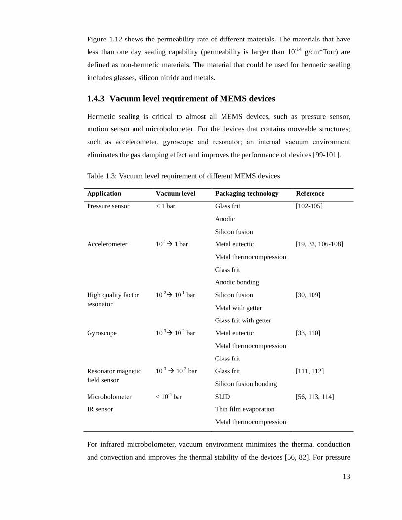
Table 1.3: Vacuum level requirement of different MEMS devices
Application Vacuum level Packaging technology Reference
Pressure sensor < 1 bar Glass frit
Anodic
Silicon fusion
[102-105]
Accelerometer 10-1� 1 bar Metal eutectic
Metal thermocompression
Glass frit
Anodic bonding
[19, 33, 106-108]
High quality factor resonator
10-2� 10-1 bar Silicon fusion
Metal with getter
Glass frit with getter
[30, 109]
Gyroscope 10-3� 10-2 bar Metal eutectic
Metal thermocompression
Glass frit
[33, 110]
Resonator magnetic field sensor
10-3 � 10-2 bar Glass frit
Silicon fusion bonding
[111, 112]
Microbolometer
IR sensor
< 10-4 bar SLID
Thin film evaporation
Metal thermocompression
[56, 113, 114]
For infrared microbolometer, vacuum environment minimizes the thermal conduction
and convection and improves the thermal stability of the devices [56, 82]. For pressure

LUU, Solid Liquid interdiffusion wafer-level bonding for MEMS packaging
14
sensor, an internal vacuum environment is needed in order to perform a reference for
pressure measurement. The requirement of vacuum level for different MEMS devices is
shown in table 1.3.

15

LUU, Solid Liquid interdiffusion wafer-level bonding for MEMS packaging
16

17
2 Methodology
2.1 Cu-Sn SLID bonding
Cu-Sn solid liquid interdiffusion (SLID) bonding is based on rapid intermetallic
compounds (IMCs) formation between Cu and Sn. The bonding process is performed at
temperatures 250-300 oC [79, 82, 85, 115-118], which is above the melting point of Sn
(232 oC). At the bonding temperature, Sn melts; Cu diffuses into Sn and reacts with Sn
to form IMCs. The resulting final bond-line consists of Cu and IMCs with elevated
temperature stability.
a b
Figure 2.1: Equilibrium phase diagram of Cu-Sn binary systems and cross-section micrograph of Cu-Sn bonded samples.
Figure 2.1 shows equilibrium phase diagram Cu-Sn binary systems and cross section
micrograph of final Cu-Sn bonded samples. The two IMCs that form during Cu-Sn

LUU, Solid Liquid interdiffusion wafer-level bonding for MEMS packaging
18
bonding process are Cu3Sn and Cu6Sn5 with the temperature stability up to 676oC and
415oC respectively. The final bond consists of IMCs and an excess Cu layer to isolate
the IMCs layer from adhesion layer and to ensure that the final bond has high
temperature stability. Cu-Sn is becoming an attractive technique for MEMS packaging
due to low cost and high performance (high bond strength, reliable hermeticity, high
temperature stability and long term reliability). In addition, compares to other SLID
bonding processes, the phase diagram is simpler and thus the formation of IMCs during
bonding process is easier to predict and describe. Cu-Sn SLID bonding with high bond
strength, reliable hermeticity has been demonstrated for MEMS packaging,
interconnection and 3D integration [82, 85, 115, 119, 120].
In the scope of this thesis, Cu-Sn SLID wafer-level bonding has been demonstrated for
hermetic encapsulation of MEMS devices. The high temperature mechanical integrity
has also been proven however further reliability testing is required to prove the method
for high temperature applications. IMCs formation during the Cu-Sn bonding process
was fully investigated. The development of IMCs during bonding process was modeled
as a function of initial Sn thickness and temperature profile. This modeling is a
powerful tool for process design and optimization. Actual bonding experiments were
demonstrated for hermetic encapsulation and high temperature applications.
2.2 Au-In SLID bonding
Au-In SLID bonding is based on the intermetallic compounds formation of Au and In.
Due to the low melting point of In (156 oC), the bonding process could be performed at
low temperatures (< 200 oC) [90, 91, 121-123]. This is of interest for many applications
since lower bonding temperature reduces thermal stress in the package, and also
facilitates bonding of temperature sensitive devices [81]. Another advantage is that an
Au rich phase could be formed during processing and thus increases the maximum re-
melting temperature of the final bond. Figure 2.2 shows the binary phase diagram of
binary Au-In systems, presents a complex system with more than 10 different
equilibrium phases. The Au-rich IMCs could have temperature stability up to 500 oC.

19
Figure 2.2: Equilibrium phase diagram of Au-In binary systems.
A typical cross-section micrograph of an Au-In bonded sample is shown in Figure 2.3.
For Au-In, an initial In surplus thickness design is considered in order to tolerate the
rapid formation of AuIn2 which occurs even at room temperature. Therefore, different
from “standard” SLID requirement, there is no Au surplus in the final bond-line. The
formation of IMCs bonding is more difficult to predict due to complex phase diagram.
Therefore, for this actual bonded sample, the final bond-line consists of four different
IMCs, which is non-equilibrium.
Figure 2.3: Cross-section micrograph of Au-In bonded samples with four IMCs present [91].
In this thesis, initial Au-In bonding is being demonstrated. The formation of AuIn2
during bonding process was modeled as a function of initial In thickness and

LUU, Solid Liquid interdiffusion wafer-level bonding for MEMS packaging
20
temperature profile. The mechanical integrity of Au-In bonded samples at high
temperature was investigated.
2.3 Intermetallic formation during SLID bonding process
Intermetallic formation is one of the critical issues of SLID bonding. The principle of
SLID bonding is based on the IMCs solidification at the bonding temperature, when the
low melting component (ML) melts. In order to obtain successful bonding, there must be
pure ML available at the surface when the melting temperature of ML (TL) is reached.
However, in a SLID bonding process, the temperature is raised following a defined
temperature profile. The IMCs are formed during the ramping process, even at a
temperature below TL, and ML is consumed into IMCs. The challenge is predicting how
much ML remains at the melting point TL which does not only depend on the initial ML
thickness, but also the temperature profile or the amount of ML that has been consumed
to form the IMCs. Therefore, the formation of IMCs during bonding process must be
well understood. In order to optimize the bonding process, there is a need of a
simulation model for IMCs development during the SLID bonding process which can
predict remaining ML thickness.
2.3.1 IMCs growth kinetic coefficients
The general mechanism of IMCs formation during SLID annealing process is itself well
understood [124]. The formation rate of IMCs depends on both the diffusion rate and
actual chemical reaction kinetics. By assuming simplification to one-dimension
diffusion model, the kinetics model of IMCs growth thickness can be expressed by:
��� − ��� = ����� �� Eq 2. 1
Where �� is IMCs thickness, �� is initial IMCs thickness, t is annealing time at
temperature T, �� is diffusion coefficient, Q is activation energy, R is the gas constant
and n is an empirical coefficient; n = ½ corresponds to a direct solution of Fick’s law,
the introduction of the empirical coefficient n opens for modeling an experimentally
observed time-dependent that deviates from a purely-diffusion controlled one.

21
The kinetics coefficients of IMCs growth thickness can be estimated by annealing the
sample at different temperatures and times. Further information is presented in our
articles [124, 125]. The estimated kinetics coefficients of IMCs during Cu-Sn and Au-In
annealing process are shown in Table 2.1 and Table 2.2. Note that for Cu-Sn systems,
different values of n were obtained. This indicates that the IMCs formation is controlled
by the combination between diffusion and chemical reaction mechanisms. At low
temperatures, the chemical reaction rate is low and slowing down the growth of IMCs, a
lower value of n was obtained. At high temperature, the chemical reaction rate is fast
and the effect of the chemical reaction is eliminated. Therefore, the diffusion
mechanism dominates and n = ½ was obtained.
Table 2.1: Kinetics coefficients of Cu3Sn growth thickness and the amount of Sn that reacts with Cu to form IMCs [124]
Cu3Sn Reacted Sn
Diffusion coefficient k0 [µm2/min2n]
7.9×10⁶ 2.8×10⁴
Activation energy Q [kJ/mol. K] 78 52
Empirical exponent n 0.5 for T>=232oC 0.45 for T>=180oC
0.4 for T<232oC 0.3 for T<180oC
Table 2.2: Kinetics coefficients of AuIn2 thickness growth, adapted from Zhang [121]
k0 (cm2/s) Q (eV) n
T>150oC 6.43 × 10� 0.46 0.5
T<150oC 1.20 × 10� 0.23 0.5
2.3.2 Modeling of IMCs development during bonding process
The objective of bonding process modeling is to build a mathematical tool used for
bonding process design and optimization. The simulation model for IMCs development
during the SLID bonding process was built based on the kinetics coefficients shown in
Table 2.1 and Table 2.2, using a numerical method. For any given time t with assuming
given IMCs thickness yt and temperature Tt; with further assuming initial zero thickness
(y0 = 0), the required time that the sample has to be annealed at Tt in order to obtain
IMCs yt could be estimated by:

LUU, Solid Liquid interdiffusion wafer-level bonding for MEMS packaging
22
��� = � ����������
���� Eq 2. 2
For a small time period from t to t+dt, we can assume that the temperature is kept at
constant dt. Using the extrapolation method, the IMCs or reacted Sn thickness at t+dt
could be estimated by:
��� � = !������" ��� + $ %��� Eq 2. 3
An example of the simulation result of IMCs development during Cu-Sn bonding
process is shown in Figure 2.4, where the IMCs thickness (Cu3Sn and Cu6Sn5) and the
remaining Sn thickness are described as a function of bond temperature profile and
initial Sn thickness. With this simulation, we can predict the critical parameters of the
bonding process:
� Remaining Sn thickness when the melting point of Sn is reached
� When all Sn is consumed into IMCs
� When the final Cu/Cu3Sn/Cu bond-line is achieved
For Cu-Sn SLID bonding, to obtain a successful bonding, it is important to ensure that
there is remaining pure Sn at the bond interface when the melting point of Sn is reached.
In addition, the objective is to achieve final Cu/Cu3Sn/Cu bond-line that is
thermodynamic stable since no IMCs will be further formed during operation process.
Therefore, the model is a powerful tool for the initial design and optimization of Cu-Sn
bonding process.
In a Cu-Sn system, both Cu3Sn and Cu6Sn5 coexist for a given time. However, in Au-In
system, the first IMC that forms during the bonding process is AuIn2 and this IMC
would be stable if there is excess In [126-129]. Other IMCs would be formed after
AuIn2 if there is excess Au. In addition, the formation of IMCs during the Au-In
bonding process is more complex to understand due to complex phase diagram.
Therefore, it is more complicated to achieve the most desired final bond structure. In the
modeling, only AuIn2 is taken into account. Figure 2.5 shows the simulation interface
for IMCs growth during Au-In bonding process.
23
Figure 2.4: Simulation of IMCs development of Cu-Sn SLID bonding process. IMCs and Sn thickness are described as functions of temperature profile and initial Sn thickness. At t1, all Sn is consumed into IMCs. At t2, the final Cu/Cu3Sn/Cu bond-line is achieved. The modeling is published in article 1 [124].
a b
Figure 2.5: a)AuIn2 thickness development at room temperature storage and b) AuIn2 thickness development during bonding process. Note that, in this simulation, only AuIn2 growth is taken into account. When AuIn2 reaches the maximum thickness, the reaction may continue and other Au-rich phases are formed. The modeling is not published.

LUU, Solid Liquid interdiffusion wafer-level bonding for MEMS packaging
24
2.4 Design rules for SLID wafer-level bonding
2.4.1 Material selection
Two material systems that have been investigated in this thesis work are Cu-Sn and Au-
In SLID. In the section below, the advantages and disadvantages of each material
system will be presented.
Using a symmetric Cu-Sn SLID bonding enables a flux-less bonding. This technique is
suitable for hermetic encapsulation and packaging of devices, which operate at high
temperature. The most important advantage of Cu-Sn SLID is low cost compared to
other SLID bonding techniques, such as Au-In, Au/Sn. Both metals used are low cost
and can be deposited by using an electroplating process. In addition, the IMCs
formation during bonding process is simple compared to other SLID systems, such as
Ag/In, Au/Sn and Au-In, with only two equilibrium phases: Cu3Sn and Cu6Sn5.
Therefore, the bonding process is easily controlled. However, the limitation of this
bonding technique is thick metal layer requirements (compared to thermocompression).
Normally, the thickness of the final bond-line is up to above 10 µm.
Au-In SLID bonding is addressed to MEMS hermetic encapsulation. The most
important advantage of this technique is the low bond temperature. Au-In can perform a
strong and hermetic bonding at temperatures below 200 oC. Low process temperature
reduces the thermal stress that occurs during bonding process and addressed to the
packaging of temperature sensitive devices. Another advantage of Au-In bonding is that
the strong and hermetic bond can be performed by using thin Au-In layer thicknesses.
The successful bonding can be obtained with 1µm Au. However, the cost of this
bonding technique is high. The two metals used are relatively expensive. In addition,
Indium is sensitive to oxidation and requires deposition in an inert atmosphere.
2.4.2 Metal thickness design
2.4.2.1 Cu-Sn design principle
Requirements for Cu-Sn SLID bond structure design:
� Symmetric bond structure is used in order to enable flux-less bonding [87]. In a
symmetric structure, Sn is deposited on both wafers.

25
� The initial Sn thickness must be above the critical Sn thickness to ensure there is
Sn remaining on the surface when the melting point of Sn is reached. The
critical Sn thickness depends on temperature profile and could be estimated by
using IMCs modeling.
� For Cu-Sn SLID bonding, the desired final bond-line is Cu/Cu3Sn/Cu.
Therefore, the Cu-Sn thickness ratio must be larger than 1.32, the ratio of Cu-Sn
thickness for full conversion to Cu3Sn is estimated by:
�&'�(� = )&'"&'*(�%)(�"&'*(�%+(�+&' = 1.32 Eq 2. 4
Here �&' and �(� are required Cu and Sn thickness, )&'"&'*(�% and )(�"&'*(�% are Cu
and Sn mass in Cu3Sn, +&' and +&' are Cu and Sn mass density.
Figure 2.6: Requirements of Cu-Sn SLID bond structure design.
2.4.2.2 Au-In design principle
The requirements of Au-In SLID bond structure design are presented in Figure 2.7.
Different from Cu-Sn bonding, In is only deposited on one wafer and the final bond
only consists of IMCs.
� For Au-In, the most critical challenge is rapid formation of AuIn2, which may
consume all In into IMC and cause fail bonding, even at room temperature
storage. There are two solutions to tolerate the formation of AuIn2: 1) use Ti as
diffusion barrier between Au and In to eliminates the formation of AuIn2 at room
temperature [121]; 2) design Au-In thickness with surplus In to ensure there is In
remaining on the surface prior to bonding. This contradicts to “standard” SLID

LUU, Solid Liquid interdiffusion wafer-level bonding for MEMS packaging
26
requirement with surplus high melting component. In this work, solution 2 is
selected. Therefore the In/Au initial thickness ratio must be larger than 3.1 – is
the In/Au thickness for full conversion to AuIn2 and estimated by:
�,�� = ),�"-',�.%)-'"-',�.%+-'+,� = 3.1 Eq 2. 5
Here �,� and �-' are In and Au thickness, ),�"-',�.% and )-'"-',�.% are In and
Au mass in AuIn2, +,� and +-' are In and Au mass density.
With In/Au thickness ration larger than 3.1, In surplus AuIn2 formation.
Therefore, even all Au reacts with In to form AuIn2, there is pure In available
prior to the bonding.
� There should be pure In available on the surface when the melting point of In is
reached.
� The overall In/Au thickness ratio depends on the targeted final bond interface.
For examples, for the targeted IMC is AuxIny, the required In/Au thickness is
estimated by:
�,��-' = ),�"-'/,�0%)-'"-'/,�0%+-'+,� Eq 2. 6
Here �,� and �-' are In and Au thickness, ),�"-'/,�0% and )-'"-'/,�0% are In
and Au mass in AuxIny, +,� and +-' are In and Au mass density. Table 2.3 shows
the required In/Au thickness ratio for different targeted IMCs.
Table 2.3: Required Au-In thickness ratio for different targeted IMCs
Phase 123/156 723/756
AuIn2 54/46 3.1
AuIn 37/63 1.34
γ (Au7In3) 20/80 0.66
ε 15.5/84.5 0.49
β1 14/86 0.43
ζ 8/92 0.23
α1 5/95 0.14

27
Figure 2. 7: Design principle for Au-In SLID bonding
2.4.3 Metal deposition
Two metal deposition methods were used in this thesis: electroplating and thermal
evaporation.
For Cu-Sn bonding, thick metal thickness is required. Therefore the electroplating
method is selected. Photoresist AZ4562 was used as the mask and Au was used as the
seed layer for the electroplating process. In order to avoid Cu oxidation, the Sn is
electroplated immediately after Cu electroplating. The Cu-Sn wafer fabrication process
is shown in Figure 2.8.
Figure 2. 8: Cu-Sn wafer fabrication process
Figure 2. 9: Au-In wafer fabrication process

LUU, Solid Liquid interdiffusion wafer-level bonding for MEMS packaging
28
For Au-In bonding, the thickness of In layer is thin, thermal evaporation method was
selected for metal deposition. The Au-In wafer fabrication process is shown in Figure
2.9. Photoresist was used as mask for In thermal evaporation. After evaporation,
photoresist was removed by lift-off process.
2.4.4 Bonding process
For both Cu-Sn and Au-In bonding, a two-steps bond temperature profile was selected
in order to reduce squeeze out of Sn and In. A description of the two-steps bond
temperature profile is shown in Figure 2.10. The temperature is raised to the contact
temperature Tc where the wafers are brought into contact and bond pressure is applied.
The contact temperature is below the the melting point of low melting component Tm.
Wafers are kept at Tc for several minutes and then raised to the bonding temperature Tb
that is above Tm. When the bonding process is finished, the temperature is ramped down
and bond pressure is released.
Figure 2.10: Typical two steps SLID bonding profile. In a two steps bond profile, the temperature is ramped up to the contact temperature Tc that is below the melting point of low melting component Tm. At contact temperature, the wafers are brought into contact and bond pressure is applied. Wafers are kept at Tc for several minutes. Then, the temperature is ramped up to bonding temperature Tb which is above the melting point of the low melting component.

29
2.5 Characterization of bond performance
2.5.1 Cross-section investigation
Cross-section characterization is a common method to investigate the microstructure of
bonded samples, the voids formation during bonding process and the material changes.
In this study, the cross-section of the SLID bonded samples is investigated by using
optical microscope, SEM and EDS. Optical microscope is used for general observation
of the bond interface. With a well-prepared cross-section, voids formation could be
observed by optical microscopy. SEM and EDS were used for further investigation of
the intermetallic composition. The cross-section of the samples was prepared by using
mechanical polishing and ion milling methods.
2.5.1.1 Mechanical grinding/polishing
Mechanical grinding/polishing is the traditional method to prepare cross-sections. The
sample is molded in Struers EpoFix and cured at room temperature for 8-9 hours. The
molded sample is grinded using SiC paper. One of the challenges of mechanical
polishing is that the sample is damaged by mechanical force. In order to avoid this
mechanical effect, the sample is hold carefully and grinded slightly during polishing
process. Three grinding steps are used using different SiC paper with different
roughness. Finally, sample is polished using diamond powder (Ø3 µm and Ø1 µm).
Figure 2.11 shows the typical cross-section micrograph of a Cu-Sn bonded sample,
which is prepared by mechanical polishing. The final Cu/Cu3Sn/Cu bond-line is clearly
observed. However, the contaminants from mechanical grinding/polishing process can
fill the voids and holes. Therefore, as shown in Figure 2.11, for typical mechanical
grinded/polished samples, the voids could not be observed.
Figure 2.11: Cross-section of a Cu-Sn bonded sample prepared by mechanical polishing. Three different layers: Cu, Cu3Sn and Cu are clearly observed. Sample is bonded by Sensonor As.

LUU, Solid Liquid interdiffusion wafer-level bonding for MEMS packaging
30
2.5.1.2 Ion milling
In addition to mechanical polishing method, Hitachi Ion miller IM4000 was used for
preparing cross-section. A visible picture of the equipment is shown in Figure 2.12.
There are two different ion milling modes: flat milling and cross-section milling. The
Argon ion gun is used to remove material. On the specimen stage, we can adjust the
eccentricity distant (distant from the center of the sample to the center of the ion beam)
and angle of the sample. On the control panel, we can set up and adjust Ar gas flow,
milling time, accelerated voltage, discharged voltage and milling mode.
Figure 2. 12: Hitachi Ion miller IM4000.
Flat ion milling
Flat milling is used to further polish the cross section of samples prepared by
mechanical grinding/polishing. An illustration of flat milling mode is shown in Figure
2.13. During the milling process, the samples holder iterates around the rotation center
with specimen iteration angle±9 (the angle of the movement from the center of
specimen) and specimen iteration speed : (the number of movements per min). The ion
gun bombards the samples surface and removes the material on the surface. The milled
area is dependent on the ion beam irradiation angle (;% and the amount of eccentricity.
The milling rate is dependent on the acceleration voltage (V) and gas flow (R).

31
Figure 2.13: Schematic of flat mode milling configuration [130].
Flat milling mode F4 [130] (specimen iteration speed : = 15 reciprocations/min and
specimen angle 9 = ± 60o) was selected. Two steps milling was used. The parameters of
each step are shown in Table 2.4. The first milling step, a small ion beam irradiation
angle (;=60o) and high-accelerated voltage (6 kV) were used in order to remove the
material and contaminants on the surface. The second milling step, a large ion beam
irradiation angle and lower accelerated voltage were used in order to polish and achieve
uniformity of the flat surface. The micrograph of a cross-section sample after flat
milling is shown in Figure 2.14. Different from typical mechanical grinded/polished
samples, the voids are clearly observed for the flat milled samples.
Table 2.4: Parameters of two steps flat milling for samples polishing.
Mode Voltage < Gas flow time
Step 1 F4 6 kV 60o 0.09 cm3/min 5 min
Step 2 F4 4 kV 80o 0.09 cm3/min 20 min

LUU, Solid Liquid interdiffusion wafer-level bonding for MEMS packaging
32
Figure 2.14: Cross-section of Cu-Sn bonded sample prepared by mechanical polishing and further polished by flat ion milling. Different material layers (Cu, Cu3Sn, Cu6Sn5) and the interface between these layers are
clearly observed. The voids in the bond interface are clearly observed after flat milling. The sample is bonded
by Sensonor As.
Cross section milling
The Cross-section milling mode is used to prepare cross-section samples directly from
diced sample. Illustration of cross-section milling mode configuration is shown on
Figure 2.15. The sample is mounted to the sample holder. A hard metal plate was used
as blocking plate. During the milling process, the holder rotates around the center with
swing speed : (the number of swings per minute) and swing angle±9. The ion gun
bombards the samples and removes the material layer by layer.
Figure 2.15: Schematic of cross-section milling mode configuration [130]
In this study, the cross-section milling mode C6 (swing speed : = 23 reciprocation/min
and swing angle 9 = ± 40o) was used. The milling parameters are shown in Table 2.5.
33
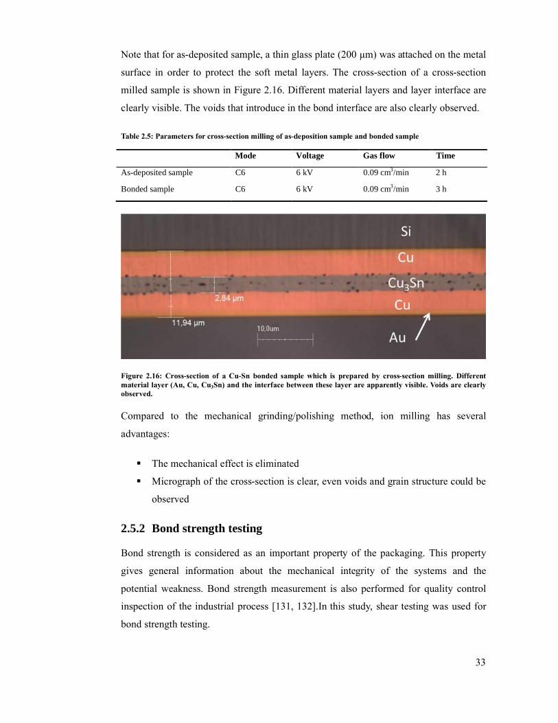
Note that for as-deposited sample, a thin glass plate (200 µm) was attached on the metal
surface in order to protect the soft metal layers. The cross-section of a cross-section
milled sample is shown in Figure 2.16. Different material layers and layer interface are
clearly visible. The voids that introduce in the bond interface are also clearly observed.
Table 2.5: Parameters for cross-section milling of as-deposition sample and bonded sample
Mode Voltage Gas flow Time
As-deposited sample C6 6 kV 0.09 cm3/min 2 h
Bonded sample C6 6 kV 0.09 cm3/min 3 h
Figure 2.16: Cross-section of a Cu-Sn bonded sample which is prepared by cross-section milling. Different material layer (Au, Cu, Cu3Sn) and the interface between these layer are apparently visible. Voids are clearly
observed.
Compared to the mechanical grinding/polishing method, ion milling has several
advantages:
� The mechanical effect is eliminated
� Micrograph of the cross-section is clear, even voids and grain structure could be
observed
2.5.2 Bond strength testing
Bond strength is considered as an important property of the packaging. This property
gives general information about the mechanical integrity of the systems and the
potential weakness. Bond strength measurement is also performed for quality control
inspection of the industrial process [131, 132].In this study, shear testing was used for
bond strength testing.

LUU, Solid Liquid interdiffusion wafer-level bonding for MEMS packaging
34
Shear testing is a common method to characterize the bond strength of a bonded sample.
This is a fast, robust, simple and cost-effective test method. The important parameters of
shear testing are: test height (the height of the shear tool from substrate), test speed (the
speed of shear tool movement), sample alignment and the tested temperature. In this
study, we used NordsonDage 4000Plus shear-tester for the shear test.
2.5.2.1 Test vehicles design for shear testing
The test vehicles design for shear test is shown in Figure 2.17. Chip size is 1.8 x 3.4
mm2 and substrate size is 6 x 6 mm2. Each substrate and die contains two bond pads
with pad size is 0.8 x 1.0 mm2.
Figure 2.17: Test vehicles design foe shear strength measurement at elevated temperature.
2.5.2.2 Shear testing configuration
The test configuration of the shear tester is shown in Figure 2.18. A customized-holder
is used to align the sample and prevent the rotation of the sample during shear test. The
samples holder is attached to a hot plate. The temperature of the hot plate is controlled
by a proportional-integral-derivative (PID) controller. A test height of 75 µm and a shear
speed of 10 µm/s were used. The shear strength of the bond is calculated by:
=( = >(? Eq 2. 7
Where FS is the recorded shear force when the fracture occurs and A is bonded area.

35
Figure 2.18: Illustration of shear test configuration. The bonded sample is attached and clamped to the hot
plate, using a customized sample holder. The holder will reduce any misalignment of the die and prevent the
rotation of the tested die during shear process. A PID controller controls the temperature of the hot plate. The
entire temperature range was calibrated to ensure that the actual measured temperature on hot plate matches
the indicated temperature on PID controller.
2.5.2.3 Temperature calibration
The calibration of the hot plate temperature was carried out in order to examine the PID
indicator temperature. Different temperatures from room temperature to 300 oC were set
up by PID. The actual hot plate temperature was measured by a thermometer. Figure
2.19 shows the measured temperature as a function of PID indicator temperature,
showing that the actual temperature is linear dependent on indicator temperature. There
is a slight difference between set up temperature and measured temperature. However,
in our case, the difference is at acceptable level.
Figure 2. 19: The measured temperature as a function of PID indicator temperature.
LUU, Solid Liquid interdiffusion wafer-level bonding for MEMS packaging
36
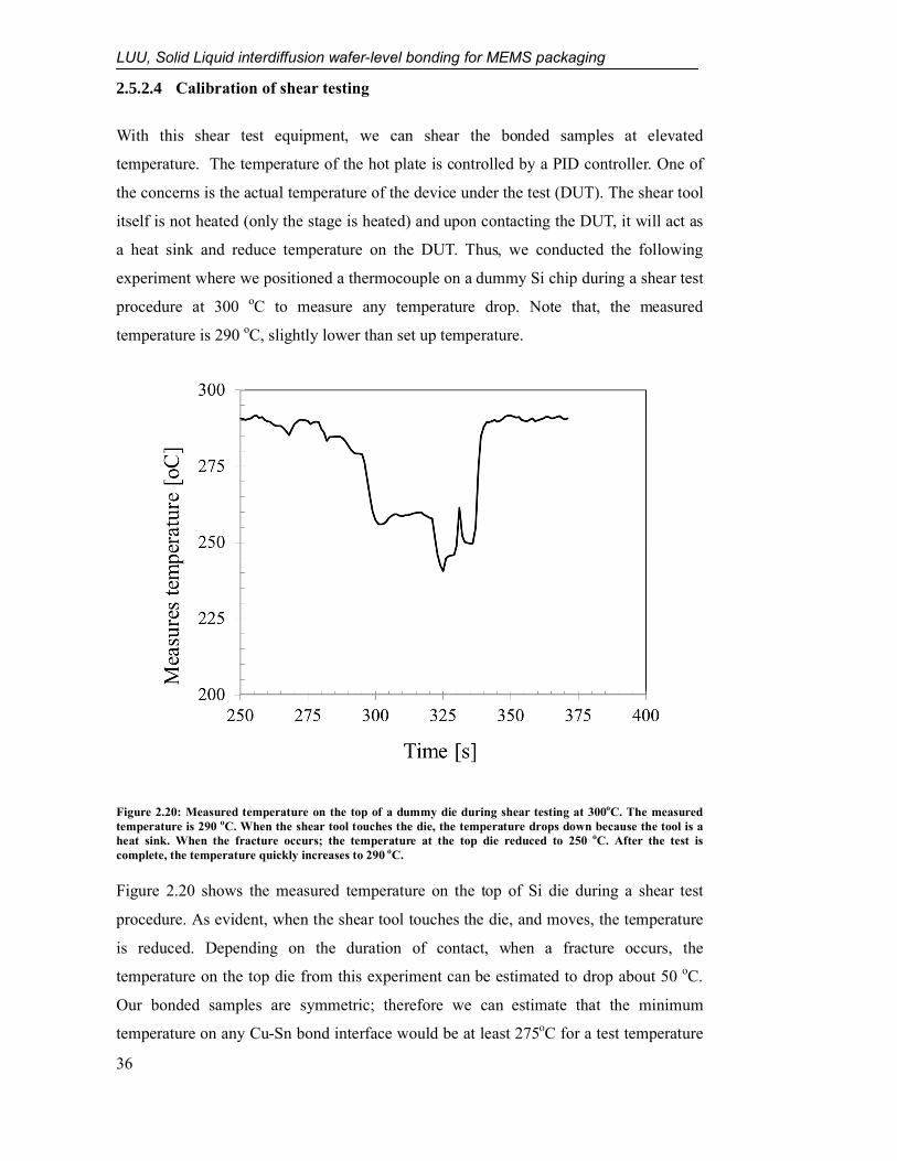
2.5.2.4 Calibration of shear testing
With this shear test equipment, we can shear the bonded samples at elevated
temperature. The temperature of the hot plate is controlled by a PID controller. One of
the concerns is the actual temperature of the device under the test (DUT). The shear tool
itself is not heated (only the stage is heated) and upon contacting the DUT, it will act as
a heat sink and reduce temperature on the DUT. Thus, we conducted the following
experiment where we positioned a thermocouple on a dummy Si chip during a shear test
procedure at 300 oC to measure any temperature drop. Note that, the measured
temperature is 290 oC, slightly lower than set up temperature.
Figure 2.20: Measured temperature on the top of a dummy die during shear testing at 300oC. The measured
temperature is 290 oC. When the shear tool touches the die, the temperature drops down because the tool is a
heat sink. When the fracture occurs; the temperature at the top die reduced to 250 oC. After the test is
complete, the temperature quickly increases to 290 oC.
Figure 2.20 shows the measured temperature on the top of Si die during a shear test
procedure. As evident, when the shear tool touches the die, and moves, the temperature
is reduced. Depending on the duration of contact, when a fracture occurs, the
temperature on the top die from this experiment can be estimated to drop about 50 oC.
Our bonded samples are symmetric; therefore we can estimate that the minimum
temperature on any Cu-Sn bond interface would be at least 275oC for a test temperature

37
of 300 oC. Further characterization of temperature at the DUT was not carried out, as we
view the results satisfactory to and the test setup repeatable since it will be identical for
all temperatures.
2.5.3 Fractography
Fractography is the investigation of the sheared fracture surfaces. This is an effective
method to determine the fracture mode of the sheared sample and the weakest material
or interface of the bonded sample. In this study, optical microscope, interferometer,
SEM and EDS were used for fracture characterization.
An example of a fractography analysis of an Au-In sheared sample is shown in Figure
2.21. The optical microscopy picture and EDS analysis shown in Figure 2.21a indicates
that there are three different fracture surfaces. The height profile in Figure 2.21b
indicates that these surfaces have different height, and each surface is planar. We can
extract the area fraction of these fracture surfaces by using bearing ratio analysis.
The filter bearing ratio analysis calculates the bearing ratio tp, the ratio of the bearing
area to the total surface area. The bearing area is the area of the surface cut by a plane at
a particular height [133]. The bearing curve shows tp in relation with the profile level.
For this particular sample, the total bond pad area is 66.5 %. The fraction of each
fracture surface area could be estimated by:
@A∗ = CA∗CA�D�EF Eq 2. 8
Where CA∗ is the bearing ratio of surface *, CA�D�EF is total bearing ratio of the pad. For
this particular case, the area fraction of surface a, b and c are 18.8 %, 66.2 % and 15 %
respectively.

LUU, Solid Liquid interdiffusion wafer-level bonding for MEMS packaging
38
a. Microscope picture and SEM
analysis b. Height profile
c. Bearing ration analysis
Figure 2.21: Fractography of an Au-In sheared sample a. microscope picture and SEM analysis, b. height profile and c. bearing ratio analysis
The bearing ratio only takes into account the measureable data. In the case the fracture
surface contains the regions that the height could not be measured by interferometer, the
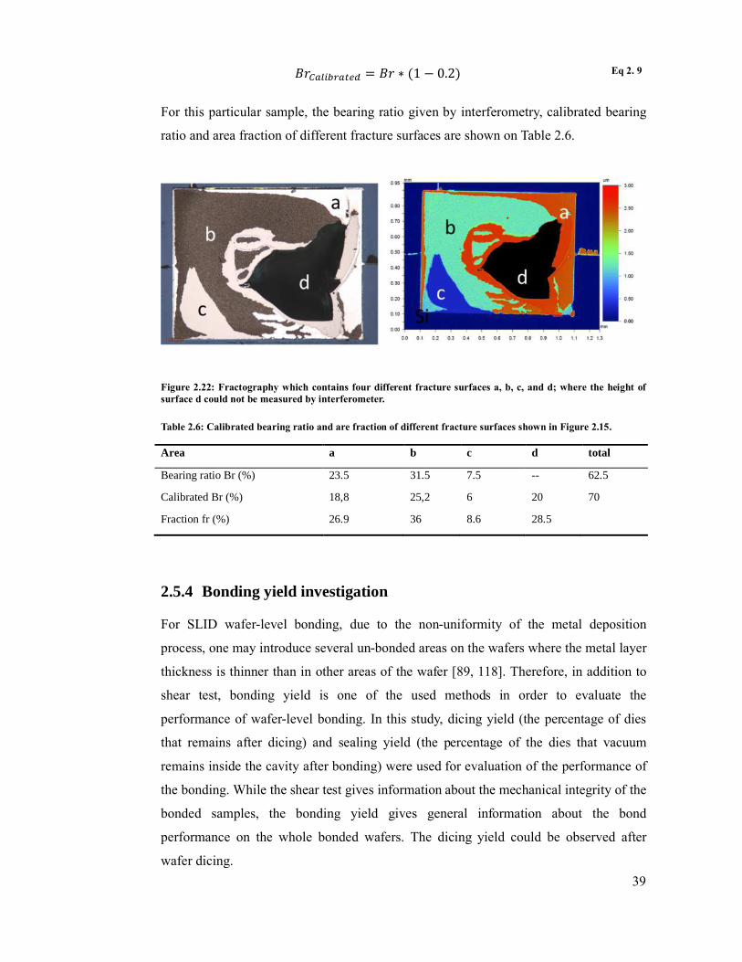
bearing ratio must be calibrated. One example of this fracture surface is shown in Figure
2.22. The fracture surface contains four different fracture modes a, b, c and d; where the
height of surface d could not be measured by interferometer. The area fraction of this
surface (d) over total area is 20 %. The calibrated bearing ratio (Br_calibrated) is
estimated by:
0 20 40 60 80 100-0.5
0
0.5
1
1.5
2
2.5
3
3.5
Percentage data cut [%]
Hei
ght [
µm]
66.5 %56.5 %12 %
Si
a
b
c
39
CA&EFGHIE�� = CA ∗ "1 − 0.2% Eq 2. 9
For this particular sample, the bearing ratio given by interferometry, calibrated bearing
ratio and area fraction of different fracture surfaces are shown on Table 2.6.
Figure 2.22: Fractography which contains four different fracture surfaces a, b, c, and d; where the height of
surface d could not be measured by interferometer.
Table 2.6: Calibrated bearing ratio and are fraction of different fracture surfaces shown in Figure 2.15.
Area a b c d total
Bearing ratio Br (%) 23.5 31.5 7.5 -- 62.5
Calibrated Br (%) 18,8 25,2 6 20 70
Fraction fr (%) 26.9 36 8.6 28.5
2.5.4 Bonding yield investigation
For SLID wafer-level bonding, due to the non-uniformity of the metal deposition
process, one may introduce several un-bonded areas on the wafers where the metal layer
thickness is thinner than in other areas of the wafer [89, 118]. Therefore, in addition to
shear test, bonding yield is one of the used methods in order to evaluate the
performance of wafer-level bonding. In this study, dicing yield (the percentage of dies
that remains after dicing) and sealing yield (the percentage of the dies that vacuum
remains inside the cavity after bonding) were used for evaluation of the performance of
the bonding. While the shear test gives information about the mechanical integrity of the
bonded samples, the bonding yield gives general information about the bond
performance on the whole bonded wafers. The dicing yield could be observed after
wafer dicing.

LUU, Solid Liquid interdiffusion wafer-level bonding for MEMS packaging
40
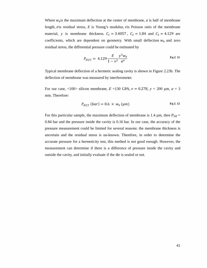
In order to investigate the sealing yield, the membrane deflection method is used to
examine if the vacuum remains inside the cavity after bonding. The test structure for
sealing yield verification is shown in Figure 2.23a. The membrane is performed on cap
wafer using silicon etching. The thickness of membrane is 200 µm. The dimension of
membrane is ~6 x 6 mm2.
Figure 2.23: Test structure design for hermetic verification by membrane deflection method and typical
membrane deflection profile of a sealed sample.
The wafers are bonded in a vacuum environment. If the wafer is hermetically sealed, the
vacuum remains inside the cavity when the bonded wafers are exposed to the
atmosphere. Due to the differential of external and internal pressures inside the cavity,
the membrane is deflected. For a square membrane, the differential pressure could be
estimated by [134]:
J GKK =M� �N�O� P + M� �N�QOR S1 − T + MQ S1 − T� �QN�OR Eq 2. 10
41
Where N�is the maximum deflection at the center of membrane, a is half of membrane
length, Pis residual stress, E is Young’s modulus, Tis Poisson ratio of the membrane
material, y is membrane thickness. M� = 3.4057 , M� = 1.84 and MQ = 4.129 are
coefficients, which are dependent on geometry. With small deflection N� and zero
residual stress, the differential pressure could be estimated by
J GKK = 4.129 S1 − T� �QN�OR Eq 2. 11
Typical membrane deflection of a hermetic sealing cavity is shown in Figure 2.23b. The
deflection of membrane was measured by interferometer.
For our case, <100> silicon membrane, E =130 GPA, T = 0.278, y = 200 µm, a = 3
mm. Therefore:
J GKK"YOA% = 0.6 ×N�"μ)% Eq 2. 12
For this particular sample, the maximum deflection of membrane is 1.4 µm, then Pdiff =
0.84 bar and the pressure inside the cavity is 0.16 bar. In our case, the accuracy of the
pressure measurement could be limited for several reasons: the membrane thickness is
uncertain and the residual stress is un-known. Therefore, in order to determine the
accurate pressure for a hermeticity test, this method is not good enough. However, the
measurement can determine if there is a difference of pressure inside the cavity and
outside the cavity, and initially evaluate if the die is sealed or not.

LUU, Solid Liquid interdiffusion wafer-level bonding for MEMS packaging
42

43
3 Summary of articles
3.1 Article I, II
Article I:
Thi-Thuy Luu, Ani Duan, Kaiying Wang, Knut E. Aasmundtveit and Nils Hoivik,
“Optimization of Cu-Sn wafer-level bonding based upon intermetallic
characterization”, 4th Electronic System-Integration Technology Conference (ESTC
2012), September 17-20, 2012, Amsterdam, Netherland.
Article II: this article is extended from article 1
Thi-Thuy Luu, Ani Duan, Knut E. Aasmundtveit and Nils Hoivik, “Optimized Cu/Sn
wafer-level bonding using intermetallic phase characterization”, Journal of Electronic
Materials 2013, Vol 42(12), 2013, pp. 3582-3592.
My contribution: literature review, design, experiment, characterization, estimation of
kinetics coefficients, numerical modeling, and manuscript preparation
For Cu-Sn SLID bonding, the formation of IMCs during bonding process is one of the
critical issues to the bond performance. The successful bonding is only obtained if there
remains pure Sn at the melting point of Sn (Tm). However, in a Cu-Sn bonding process,
the temperature is raised following a defined temperature profile. The IMCs are formed
during the ramping process, even below the Tm and an amount of Sn would be
consumed into IMCs. The challenge is to predict how much Sn remains at Tm which
does not only depend on the initial Sn thickness, but the amount of Sn that has been
consumed to form IMCs. Therefore, there is a need of a simulation model for IMCs

LUU, Solid Liquid interdiffusion wafer-level bonding for MEMS packaging
44
development during Cu-Sn bonding process, which can predict how much Sn, remains
at the melting point of Sn. The motivation of this work is to implement a numerical
simulation model for IMCs development during Cu-Sn bonding process. With this
simulation model, we can predict the critical parameters of the bond temperature
profile: the Sn thickness that remains at the melting point of Sn, the time that all Sn are
consumed to form IMCs and the time that final Cu/Cu3Sn/Cu bond-line is obtained.
Main results:
In order to simulate the IMCs thickness growth during Cu-Sn SLID bonding process,
the formation of IMCs during Cu-Sn annealing process was fully characterized. It is
well known that the two IMCs that form during Cu-Sn annealing process are Cu3Sn and
Cu6Sn5. In this study, the initial characterization focuses on growth kinetics model of
Cu3Sn growth thickness and the amount of Sn thickness that is consumed into IMCs.
The as-electroplated Cu-Sn samples were annealed at different temperatures (150 oC to
300 oC) and annealing times (0 min to 320 min). The kinetics coefficients are then
extracted from the measured IMCs thicknesses of the annealed samples.
Based upon the estimated kinetics coefficients, a numerical simulation model for IMCs
thickness development during Cu-Sn bonding process was implemented, using
MATLAB. With this simulation, the IMCs thickness (Cu3Sn and Cu6Sn5) and the
remaining Sn thickness on the surface are described as functions of initial Sn thickness
and bond temperature profile. The actual bonding experiments were carried out in order
to evaluate the simulation model. According to our characterization, the measured IMCs
thicknesses match the simulated thicknesses. This verifies the accuracy of simulation
model, and the model could be used as a tool for process design and optimization.
According to the simulation model, for an initial Sn thickness of 1.5 µm, successful
bonding could be obtained by using two steps temperature profile. In this two steps
temperature profile, the temperature is ramped to contact temperature (150 oC) where
the wafers are brought into contact and kept at 150 oC for 5 min. The temperature is
then ramped to bond temperature 270 oC. To achieve final Cu/Cu3Sn/Cu bond interface,
the bonding time should be longer than 30 min.

45
3.2 Article III
Thi-Thuy Luu, Ani Duan, Kaiying Wang, Knut E. Aasmundtveit and Nils Hoivik,
“Cu/Sn SLID wafer-level bonding optimization”, proceeding of Electronic Components
and Technology Conference (ECTC), 2013 63rd, May 28-31 2013, pp. 1531-1537.
My contribution: mask design, fabrication, characterization and analysis of experiment
result.
The objectives of this study is to further investigate the effect of different bonding
parameters, include initial Sn thickness, bond pressure and bond temperature profile to
Cu-Sn SLID bond performance. Bond performance was evaluated by bonding yield
(dicing yield: the percentage of dies that remains after dicing; sealing yield: the
percentage of dies that vacuum remains inside after bonding).
Main results:
The experimental results confirm that: high bonding yield is achieved if there is pure Sn
at the bond surface when the melting point of Sn is reached. For our actual bonding, a
Sn thickness of 1.5 µm should be used in order to minimize the squeeze-out of Sn, and
tolerate the non-uniformity during Cu/Sn plating process. A moderate bond pressure
will give high bond yield. With bond pressure of 1.5 MPa, bond temperature of 270oC
and initial Sn thickness of 1.5 µm - dicing yield of 100% and sealing yield of 80 %
waere obtained.
3.3 Article IV
Ani Duan, Thi Thuy Luu, Kaiying Wang, Knut E. Aasmundtveit and Nils Hoivik,
“Wafer-level hermetical Cu-Sn micro-joints with high mechanical strength and low Sn
flow”, submitted to Journal of Micromechanics and Microengineering.
My contribution: modelling of IMCs development during bonding process, part of mask
design and characterization, process optimization, description of modeling part in
manuscript.

LUU, Solid Liquid interdiffusion wafer-level bonding for MEMS packaging
46
The objective of this work is to demonstrate Cu-Sn SLID wafer-level bonding for
MEMS hermetic encapsulation. For hermetic encapsulation, shrinkage of sealing frame
width is one of the important issues. With small sealing frame width, the size of the
final product could be reduced and the volume of production could be improved.
However, one of the concerns is how much we can shrink the frame width; since with a
small frame width, the performance of the bonded samples could be affected. In this
study, we investigated the effect of Cu-Sn sealing frame with on bond performance. In
addition, the effect of the bond pressure and the temperature profile were further
investigated. The bond performance was evaluated by bond yield and bond strength.
Main results:
We demonstrated Cu-Sn SLID wafer-level bonding with high yield and less Sn squeeze-
out for MEMS encapsulation. The minimum frame width we could achieve is 80 µm. To
obtain high bond performance, a bond pressure higher than 1.5 MPa should be used. A
two-steps temperature profile (described in chapter 2) can reduces the squeeze-out of
Sn.
3.4 Article V
Thi Thuy Luu, Nils Hoivik, Kaiying Wang, Knut E. Aasmundtveit and Astrid-Sofie
Vardoy, “Cu-Sn SLID wafer-level bonding for high temperature application”,
manuscript accepted to be published on Metallurgical and Materials Transactions A.
My contribution: literature review, mask design, assembly, characterization and test,
analysis, and manuscript preparation.
For the applications that require operating at high temperature, long-term reliability will
be challenged due to the increase of thermal stress, material corrosion and other effects.
Therefore, it is important that the materials used in a bond-line have a high melting
point as well as a high mechanical integrity at high temperatures. Furthermore, the
bond-line should have high thermal conductivity to reduce any thermal stress in the
bond stack, and be thermodynamically stable to reduce any corrosion from diffusion at
high temperature. Cu-Sn SLID wafer-level bonding is a promising set of materials
suitable for these applications, as it enables low cost metallization, flux-free bonding,

47
high mechanical strength and hermeticity. The objective of this study is to demonstrate
Cu-Sn SLID wafer-level bonding for high temperature applications. The mechanical
integrity of Cu-Sn SLID bonded samples at elevated temperatures up to 300 oC was
investigated.
Main results:
Cu-Sn SLID wafer-level bonding results in a high yield bonding and high mechanical
integrity at high temperatures. The resulting bond strength show relatively small
variation in strength as a function of temperature, corresponding very well to the phase
diagram predicting the present phase (Cu3Sn) in the bond-line to be stable to
temperatures above 676 oC. The average measures shear strength is 45 MPa from room
temperature up to 300 oC, exceeding the MIL-STD by far. The average shear strength
does not vary significantly across the different regions of the bonded wafers. However,
at the regions with initially thinner Sn there is larger scatter in the measured shear
strength. It is believed that small un-bonded regions within the test die where the Sn
layer was at its thinnest cause this variation.
Interferometry of the fractured surfaces show brittle and well-defined planar surfaces,
either between Ti/W adhesion layer to SiO2, between Cu and Cu3Sn, or at the original
bonding interfaces. The two dominating fracture modes are in the adhesion layer and the
original bond interface. This verifies that the material systems have potential for giving
even higher bond strength than our measured strength.
This work provides experimental evidence for the stability of Cu-Sn SLID bonding at
high temperature, a stability that has long been predicted from the phase diagrams. This
strongly confirms the applicability of Cu-Sn SLID bonding for high temperature
applications.
3.5 Article VI
Thi Thuy Luu, Nils Hoivik, Kaiying Wang, Knut E. Aasmundtveit and Astrid-Sofie
Vardoy, “Characterization of wafer-level Au-In bonded samples at elevated
temperatures”, Metallurgical and Materials Transactions AJune 2015, Volume 46, Issue
6, pp 2637-2645.

LUU, Solid Liquid interdiffusion wafer-level bonding for MEMS packaging
48
My contribution: design, assembly, characterization and test, part of shear test
experiment, analysis, modeling, and manuscript preparation.
The motivation of this study is to demonstrate Au-In SLID bonding for high
temperature applications. High temperature applications are defined by the applications
that require operation at, or exposure to high temperatures above 125 oC. For these
applications, the main requirements to the bonding material are that the bond-line has a
high melting point and that the shear strength remains high at elevated temperatures. In
order to achieve high shear strength at elevated temperatures, it is important to minimize
the thermally induced stresses in the bond stack; this is typically done by reducing the
bonding temperature, having a low CTE mismatch between the utilized materials, and
by having a good thermal conductivity. One of the advantages that make Au-In bonding
interested for high temperature applications is the low temperature process. The bonding
could be assembled at 180 oC, which is lower than other SLID bonding. In this study,
the mechanical integrity of Au-In SLID bonded samples at different temperatures was
investigated.
Main results:
Au-In SLID wafer-level bonding with a proper design of the metal thicknesses for Au
and In results in a very high bonding yield and a high resulting shear strength: in the 30
MPa range. The shear strength is stable when the temperature is increased from room
temperature to 200 oC, and increases to ~40 MPa when the temperature is increased to
300 oC. This verifies experimentally that Au-In SLID bonding, performed at
temperatures right above the melting temperature of In (156 oC) is indeed very suitable
for high-temperature applications. Phase diagram predictions call for stability to 450 oC,
and we demonstrated high strength up to our highest testing temperature of 300 oC.
The bond-line consists of the intermetallic phases AuIn and γ`, as found by cross-section
microscopy and EDS. Interferometry of the fractured, sheared samples reveals that at
temperatures up to 200 oC, the samples fracture at well-defined planar surfaces: either at
the adhesion layer to intermetallic interfaces, or at the position of the original bond
interface. At 300 oC, the nature of the fracture changes to a ductile fracture, explained
by a phase transition to the ψ-phase and an annealing effect of the original bond

49
interface. The higher overall bond strength at 300 oC results from this improved strength
of the initial bond interface.
The shear strength of devices has been investigated. With a proper design of the metal
thicknesses for Au and In, a very high bonding yield was achieved. The final bond-line
has both AuIn and γ` phases present as verified by cross section microscopy and EDS
analysis. Furthermore, the die shear strength of the bonded samples was measured as
function of temperature, from RT to 300 oC. The increasing trend of shear strength from
RT to 300oC confirms that Au-In bonding is a promising technique for high-temperature
applications.

LUU, Solid Liquid interdiffusion wafer-level bonding for MEMS packaging
50

51
4 Voids characterization
4.1 Voids formation
Voids formation during bonding process is one of the important issues of Cu-Sn SLID
bonding which can affect the bond performance. The voids formation during Cu-Sn
bonding process has been reported by many research and industry groups [36, 45, 76,
78, 89, 115, 117, 135-151] and can be classified in three voids scenarios as shown in
Figure 4.1: a) bond interface voids, which distribute at the original bond interface, b)
Cu/Cu3Sn voids, also call sporadic voids and distribute as a continuous layer at
Cu/Cu3Sn interface and c) Kirkendall voids which distribute across the Cu3Sn layer. In
this section, different mechanisms of void formation will be presented and discussed.
a b c
Figure 4. 1: Three different types of voids that can form during Cu-Sn SLID bonding process a) bond interface voids, b) Cu/Cu3Sn voids and c) Kirkendall voids.

LUU, Solid Liquid interdiffusion wafer-level bonding for MEMS packaging
52
4.1.1 Bond interface voids
4.1.1.1 Bond interface voids formation mechanism
There are several mechanisms behind the formation of bond interface voids: lack of
wetting at the bond interface, growth of Cu6Sn5 scallops, non-uniformity of
electroplating process and non-uniform initial Cu-Sn thickness [143, 152-155].
Figure 4. 2: Cross-section of Cu-Sn SLID bonded samples. Interface voids are formed due to a) lack of wetting at original bond interface [152], b) non-uniformity of electroplating process [155] and c) the growth of Cu6Sn5 scallops during bond process [153].
Lack of wetting at the original bond interface
Lack of wetting at the bond interface is caused by contaminations, Sn and Cu oxidation
when Cu to Cu-Sn bonding is used [116, 152]. The oxidation issue can be solved by
using a Cu3Sn layer as protection layer to prevent Cu from oxidation or symmetric
Cu/Sn bonding [87, 156]. In this study, symmetric Cu-Sn bonding is used. Therefore,
lack of wetting at the original bond interface is not an issue for voiding.
Non-uniformity of electroplating process
For Cu-Sn SLID wafer-level bonding, the Cu-Sn layers are prepared by electroplating
process. According to our experience, there is always a degree of non-uniformity during
electroplating process. This causes a 2-10 % variation of Cu and Sn thickness. At the
regions of the wafers where Cu layer is thinnest, Sn may not contact together during
bonding process and cause un-bonded area [118, 155].

53
Growth of Cu6Sn5 scallops
During Cu-Sn SLID bonding process, the temperature is increased following a defined
temperature. During the ramping process, the Cu6Sn5 scallops grow and Sn is converted
into solid IMCs. Defined Tm is the melting point of Sn. Defined critical Sn thickness
(ycritical) is the minimum thickness to ensure that there is pure Sn at the original bond
interface when Tm reached. If the initial Sn thickness is thinner than ycritical, Cu6Sn5
scallops will reached the Sn surface before Tm is reached, and acts as spacers and cause
interface voids. This is further described in article 1 and 2.
4.1.1.2 Prevent interface voids
Pretreatment of wafers prior bonding
As described, one of the reasons of interface voids is the growth of Cu6Sn5 scallops
which occurs even at room temperature. In order to prevent interface voids, one of the
solutions is to prevent the growth of Cu6Sn5 scallops.
Figure 4. 3: IMC development during annealing process at 50 oC of as-plated Cu-Sn sample and shorted pre-annealed Cu-Sn sample, showing that short annealing at 200 oC in 1 minute can flatten IMC layer [157].

LUU, Solid Liquid interdiffusion wafer-level bonding for MEMS packaging
54
Annealing of electroplated Cu/Sn sample at temperatures 125-200 oC can produces a
thin and uniform Cu6Sn5 layer; this leads to subsequent growth of a planar IMCs instead
of scallops [148, 157]. Therefore, pre-annealing electroplated Cu-Sn sample is one of
solutions to slow-down the formation of Cu6Sn5 scallops, and prevents interface voids
formation.
Optimize initial Cu-Sn thickness and bonding process
Optimize bond temperature profile is one solution to prevent interface voids formation.
There are two issues should be taken into account:
� A two-steps bonding profile should be used [158]. In a two-steps bond
temperature profile, the wafers are brought into contact at a temperature of 150-
200 oC and kept at this temperature for several minutes. This temperature soak is
served as pre-treatment of the wafers and prevent the growth of Cu6Sn5 scallops.
� There must be pure Sn available at the surface when the melting point of Sn is
reached, in order to perform a good wetting at the interface and compensate the
non-uniformity of electroplated Cu thickness over the wafer.
Bond temperature can be optimized by using the simulation model described in this
thesis of IMCs development during the Cu-Sn bonding process. More information about
this approach is presented in chapter 2 and article 1, 2.
4.1.2 Cu/Cu3Sn voids
4.1.2.1 Cu/Cu3Sn voids formation
Cu/Cu3Sn voids are usually observed in Cu-Sn soldering and have been frequently
reported in earlier studies [78, 135, 136, 138]. Different mechanisms of these voids
formation correlates to impurities and stress-strain have been proposed [136, 139, 146,
149, 150, 159]:
� Vacancy injection mechanism: during the Cu-Sn bonding or annealing process,
the reactive of Cu and Sn occurs at Cu/Cu3Sn and Sn/Cu6Sn5 interfaces and
leaves vacancies at these interfaces. Theoretically, the vacancies would be
injected by Cu and Sn diffused atomics. The impurities can block the vacancies
injection process and voids later form [135, 139, 160, 161].

55
� Strain mechanism: Cu, Sn, Cu6Sn5 and Cu3Sn have different elasticity and
crystalline structure. During Cu-Sn annealing process, the difference of elasticity
causes the strain at Cu/Cu3Sn interface. The strain distributes at Cu grain
boundary and induces voids formation [149].
The effects of Cu grain structure, organic impurities and Cu oxidation on this type of
voids formation are experimentally confirmed [78, 135, 139, 146, 150, 159, 162, 163].
These studies demonstrated that: small Cu grain size, organic impurities and single
crystalline Cu texture can cause higher voids level at Cu/Cu3Sn interface. The possible
reasons are:
� For small Cu grain size, more Cu diffuses into IMCs through grain boundary and
more vacancies are formed at Cu/Cu3Sn interface.
� In a polycrystalline texture, the Cu has random orientations; therefore Cu
diffuses into Sn trough many different orientations and reduces voids level.
� During the Cu-Sn bonding process, the reaction between Cu and Sn mostly
occurs at Cu/Cu3Sn and Cu3Sn/Cu6Sn5 interface and results vacancies at these
interfaces. Impurities from electroplating process and cleaning chemical [161,
164] or Cu oxidation can block the vacancies injection at Cu/Cu3Sn interface
and voids later form.
Figure 4. 4: Cu/Cu3Sn voids formation due to small Cu grain size. For sample A, the grain size is small, voids
form at Cu/Cu3Sn interface after annealing [162].
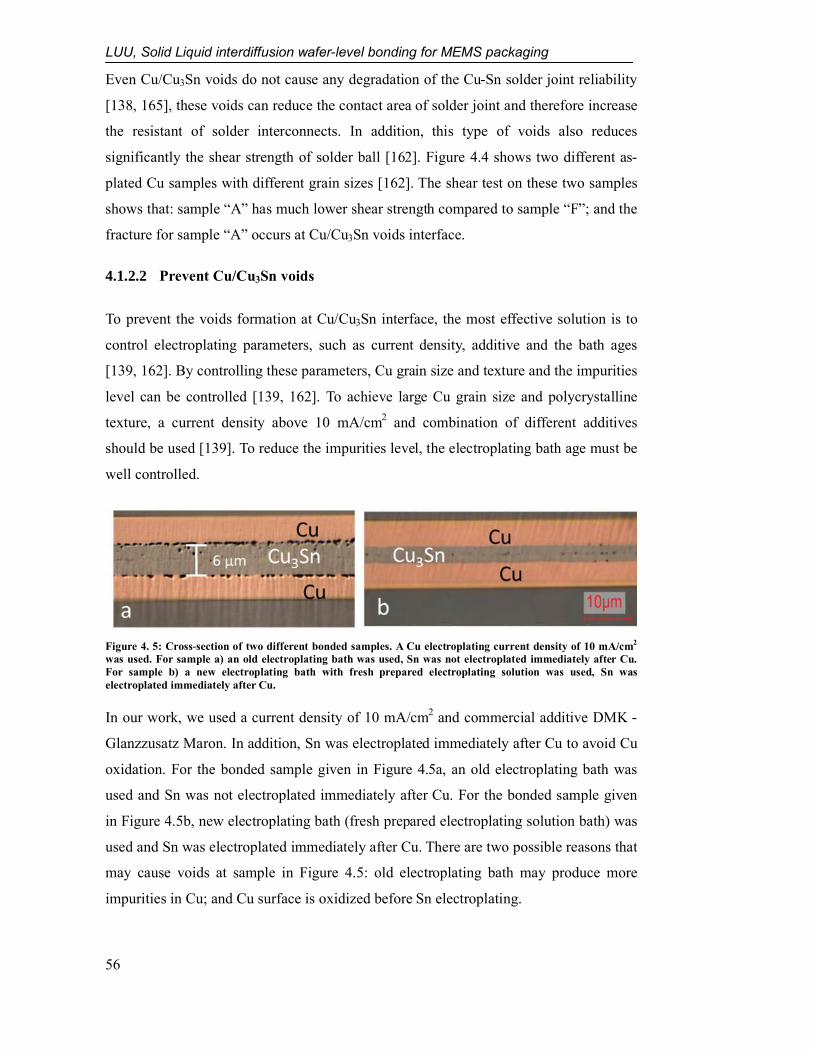
LUU, Solid Liquid interdiffusion wafer-level bonding for MEMS packaging
56
Even Cu/Cu3Sn voids do not cause any degradation of the Cu-Sn solder joint reliability
[138, 165], these voids can reduce the contact area of solder joint and therefore increase
the resistant of solder interconnects. In addition, this type of voids also reduces
significantly the shear strength of solder ball [162]. Figure 4.4 shows two different as-
plated Cu samples with different grain sizes [162]. The shear test on these two samples
shows that: sample “A” has much lower shear strength compared to sample “F”; and the
fracture for sample “A” occurs at Cu/Cu3Sn voids interface.
4.1.2.2 Prevent Cu/Cu3Sn voids
To prevent the voids formation at Cu/Cu3Sn interface, the most effective solution is to
control electroplating parameters, such as current density, additive and the bath ages
[139, 162]. By controlling these parameters, Cu grain size and texture and the impurities
level can be controlled [139, 162]. To achieve large Cu grain size and polycrystalline
texture, a current density above 10 mA/cm2 and combination of different additives
should be used [139]. To reduce the impurities level, the electroplating bath age must be
well controlled.
Figure 4. 5: Cross-section of two different bonded samples. A Cu electroplating current density of 10 mA/cm2
was used. For sample a) an old electroplating bath was used, Sn was not electroplated immediately after Cu.
For sample b) a new electroplating bath with fresh prepared electroplating solution was used, Sn was
electroplated immediately after Cu.
In our work, we used a current density of 10 mA/cm2 and commercial additive DMK -
Glanzzusatz Maron. In addition, Sn was electroplated immediately after Cu to avoid Cu
oxidation. For the bonded sample given in Figure 4.5a, an old electroplating bath was
used and Sn was not electroplated immediately after Cu. For the bonded sample given
in Figure 4.5b, new electroplating bath (fresh prepared electroplating solution bath) was
used and Sn was electroplated immediately after Cu. There are two possible reasons that
may cause voids at sample in Figure 4.5: old electroplating bath may produce more
impurities in Cu; and Cu surface is oxidized before Sn electroplating.

57
Another option to reduce voids formation is to anneal Cu at high temperature before
electroplating of Sn. Annealing Cu at 650oC or 350oC for 2h can increase Cu grain size
and gasify certain impurities inside Cu [139, 146, 159]. This produces high purity, large
Cu grain structure and subsequently reduces voids level Cu/Cu3Sn interface. In our
case, we do not use this solution due to several reasons:
� In our electroplating, we used a current density 10 mA/cm2 and commercial Cu
electroplated additive. This can produce Cu with high purity large grain size.
� Annealing Cu before Sn electroplating introduces one more fabrication step.
� For MEMS packaging and encapsulation, the devices can be damaged due to
high temperature annealing.
4.1.3 Kirkendall voids
The Kirkendall voids are formed due to the difference between the intrinsic diffusivities
of Cu and Sn in Cu3Sn, which is typical for any multiphase diffusion systems [166]. In
the Cu-Sn diffusion system, the diffusion rate of Cu into Cu3Sn is much faster than the
diffusion rate of Sn [167]. This imbalanced interdiffusion leaves atomic-level vacancies
at Cu3Sn side. Voiding is formed from the accumulation of excess vacancies.
Figure 4. 6: An illustration of Kirkendall voids formation due to the difference between the intrinsic diffusivities of Cu and Sn in Cu3Sn.
An illustration of Kirkendall voids formation mechanism is shown in Figure 4.6.
Similar to Cu/Cu3Sn voids, the Kirkendall voids are correlated to the impurities level in
Cu and Cu grain size. Small Cu grain size and high impurities introduce much higher
voids level.

LUU, Solid Liquid interdiffusion wafer-level bonding for MEMS packaging
58
4.2 Voids characterization
Figure 4.7 shows the cross sections of two different Cu-Sn bonded samples. With
samples shown in Figure 4.7 b, two types of voids are presented: Kirkendall voids and
interface voids. For these two actual samples, we clearly observe that voids area
increases with the increasing of Cu3Sn thickness. In this study, the correlation between
voids and Cu3Sn thickness is investigated. To eliminate the effect of the length of
sample and Cu thickness, the void area was described as voids fraction (area per unit
length).
Figure 4. 7: Cross section of the bonded samples which is prepared by process A. The samples were
electroplated and bonded by Sensonor As. The thickness of Cu3Sn layer is not uniform.
To estimate void fraction and Cu3Sn thickness, image processing software “ImageJ”
was used for samples analysis. The analysis process is described in Figure 4.8. The
original cross-section of the bonded sample is shown in Figure 4.8a. The original image
was split into three different colors: red, green and blue. The blue one is used for voids
area estimation, the red one is used for IMCs thickness estimation. By adjusting color
threshold of the blue, voids are presented, as shown in Figure 4.8b. These voids are
considered as particles. The software can count the number of particles and measure the
area of each particle and total area. The voids fraction (voids area per unit length) is
estimated by:
@[DG = ?[DG \ Eq 4. 1
Here, @[DG is voids area fraction per unit length, ?[DG is total voids area and L is the
length of sample.

59
By adjusting color threshold of the red, the Cu layers and Cu3Sn layer are presented as
shown in Figure 4.8c. The area of Cu3Sn layer can be measured by software. Cu3Sn
thickness is estimated by:
�,]& = ?,]&\ Eq 4. 2
Here �,]& is average Cu3Sn thickness, ?,]& is Cu3Sn area and L is length.
Figure 4. 8: Voids analysis using image processing software: a) original cross-section of the bonded samples, the original picture was split into three different colors – green, blue and red; b) cross-section picture after adjusting the color threshold of the blue, voids present as particles, software can count and measure the
volume of these particles; c) cross-section picture after adjusting the color threshold of the red; Cu3Sn layer present as center dark layer, software can measure the area of this layer.

LUU, Solid Liquid interdiffusion wafer-level bonding for MEMS packaging
60
4.3 Analysis of voids formed in wafer-level bonded samples
4.3.1 Voids analysis results
Figure 4.9 describes the voids area fraction of different Cu-Sn SLID wafer-level bonded
samples as function of Cu3Sn thickness. Two different wafer-level bonded samples were
prepared: A) samples prepared by industry partner Sensonor AS, B) samples prepared
by our work. Voids area fraction increases with the increasing of Cu3Sn thickness.
Figure 4. 9: Voids area fraction of Cu-Sn SLID wafer-level bonded samples as functions of Cu3Sn thickness. A: bonded samples prepared by industry partner Sensonor AS. B: bonded samples prepared by our work.
4.3.2 Voids development during further annealing of bonded samples
To investigate the effect of voids to the bond performance, further annealing of bonded
samples were carried out. Figure 4.10 shows the cross-sections of as-bonded sample and
further annealed sample. For this sample, we obtain a low voids area fraction of 0.01.
The voids area does not change during the annealing process; but Cu grain size has
changed after annealing. This experimentally confirms that: there is not further diffusion

61
of Cu into Cu3Sn; final Cu/Cu3Sn/Cu bond-line has high temperature stability up to 370
oC and annealing Cu at 370
oC.
Figure 4. 10: Further annealing of Cu-Sn bonded samples. Samples were prepared by process A. SEM cross-section is taken by Sensonor As.
4.3.3 Discussion
In our bonding experiment, the electroplating process was controlled and we can
prevent the formation of sporadic voids at Cu/Cu3Sn layer. Only bond interface and
Kirkendall voids were observed. The area fractions of these types of voids as functions
of Cu3Sn thickness are shown in Figure 4.11. Bond interface voids area fraction seems
not to be depended on Cu3Sn thickness and does not have significant change with
Cu3Sn thickness. The Kirkendall voids area fraction increases monotonically with
Cu3Sn thickness.

LUU, Solid Liquid interdiffusion wafer-level bonding for MEMS packaging
62
Figure 4. 11: Bond interface and Kirkendall voids area fractions as functions of Cu3Sn thickness, bonded
samples set A.
According to earlier work [78, 146, 168], with a constant annealing temperature, the
Kirkendall voids area fraction and Cu3Sn thickness have parabolic correlation with
annealing time. Therefore, Kirkendall voids area fraction should have a linearly
correlation with Cu3Sn thickness. A linear fitting of voids area fraction and Cu3Sn
thickness correlation is shown in Figure 4.12. For samples set A and set C, the voids
area fractions and Cu3Sn thickness have linear correlation. This linear trend is caused by
Kirkendall voids. For sample set B, the initial Sn thickness is thinner than set A and
cannot compensate the non-uniformity of electroplating process. This introduces voids
that come from un-bonded area and the voids area fraction does not have linear
correlation with Cu3Sn thickness.

63
Figure 4. 12: Voids fraction as function of Cu3Sn thickness A. Bonded sample from industry partner (Sensonor
As). B. Bonded sample from our work. C. from literature (G. Lim [168]).
Another mechanism that could be driving factor of voids formation is the volume
change of metallization during bonding process. The reaction between Cu and Sn
induces a volumetric change due to the differences in mass densities of Cu, Sn and
IMCs. The volume change can cause a voids area fraction ~0.1*tCu3Sn [µm2/µm]. During
the bonding process, the bond pressure is applied. This may reduce the effect of
volumetric change. Therefore, in our bonding, the voids area fraction/Cu3Sn thickness
ratio is ~0.05 (set A), much smaller than 0.1.
4.4 Conclusion
In this session, the voids formation during Cu-Sn SLID wafer-level bonding process
was presented. Even there are different voids scenarios: interface voids, Cu/Cu3Sn voids
and Kirkendall voids, the voids level have strong correlation with Cu grain structure and

LUU, Solid Liquid interdiffusion wafer-level bonding for MEMS packaging
64
impurities. By controlling Cu electroplating process, we can eliminate Cu/Cu3Sn voids
and obtain Cu-Sn SLID wafer-level bonded samples with low voids area fraction.
For this work, voids are formed due to Kirkendall effect and the growth of Cu6Sn5
scallops. The linear correlation between Kirkendall voids area fraction and Cu3Sn
thickness was experimentally verified. With a final Cu/Cu3Sn/Cu bond-line, the voids
area does not change during further annealing of bonded samples. This confirmed that
low voids area fraction does not cause degradation of the bond performance.

65

LUU, Solid Liquid interdiffusion wafer-level bonding for MEMS packaging
66
67
5 Summary and outlook
5.1 Summary
This thesis presented solid liquid interdiffusion (SLID) wafer-level bonding for MEMS
packaging. Two techniques, Cu-Sn SLID bonding and Au-In SLID bonding, have been
investigated.
5.1.1 IMCs develoment during Cu-Sn SLID bonding process
The formation of IMCs which takes place during the Cu-Sn SLID wafer-level bonding
process was successfully characterized. Thermal kinetics models of the Cu3Sn thickness
and the amount of Sn that is converted into IMCs were estimated. We experimentally
verified that the growth of IMCs during Cu/Sn annealing process follows Arrhenius
equation �� = ���^_`a ��. One of the major findings of our study is that the empirical
coefficient n depends on temperature. Above the melting point of Sn, n is equal to 1/2,
as expected from the analytical solution of the diffusion equation, corresponding to a
diffusion-controlled process. For temperatures below the melting point of Sn, a value of
n below 1/2 is obtained, indicating that slower chemical reaction limits the IMC growth
rate. Based on this knowledge of IMC formation during the annealing process, a
MATLAB model was created to simulate the IMCs development during the bonding
process. Using this simulation model, we can predict the parameters that are important
for bonding temperature profile optimization: unreacted remaining Sn thickness on each
wafer at the contact temperature and bonding temperature, and required bonding times
to achieve Cu/Cu3Sn/Cu6Sn5/Cu3Sn/Cu and Cu/Cu3Sn/Cu final bond-lines. Experiments
show that the simulation model accurately predicts the IMCs formation during the
bonding process. The experimental and simulation results show that an effective
solution to reduce the bonding time is to leave the final bond-line as

LUU, Solid Liquid interdiffusion wafer-level bonding for MEMS packaging
68
Cu/Cu3Sn/Cu6Sn5/Cu3Sn/Cu, with further annealing performed outside the wafer bonder
to convert all the Cu6Sn5 into Cu3Sn.
5.1.2 Effect of bond pressure and temperature profile to Cu-Sn SLID bond performance
We have demonstrated Cu-Sn SLID wafer-level bonding for fabricating micro-joints
with high mechanical strength. The effect of bond temperature profile, bond pressure
and Cu/Sn frame width to the bond performance was investigated. The main findings of
this work are:
� To achieve high bond strength, a high bond pressure above 1.5 MPa should be
used. For this work, with bond pressure 1.5 MPa, we can obtain a bond-strength
of 74 MPa, a dicing yield 100 % and a sealing yield of 80 %.
� A two-steps temperature profile can reduce effectively Sn squeeze out.
� In this work, the minimum frame-width we can obtain is 80 µm.
5.1.3 High-temperature mechanical integrity of Cu-Sn SLID bonds
Cu–Sn SLID wafer-level bonding results in a high bonding yield and a high mechanical
integrity; also well above the melting point of Sn. The average measured shear strength
is 42 MPa, exceeding the MIL-STD by far. For shear tests performed at temperatures
from room temperature up to 300 oC, no significant change in shear test is observed,
thus verifying the high-temperature stability predicted for Cu–Sn SLID bonding.
These high shear-strengths are obtained although there was non-uniformity in the
electroplating process that resulted in larger scattering of the shear strength at several
regions of the bonded wafer pair. The non-uniformity also caused voids and un-bonded
areas at the original bond interfaces, and led to this being one of two dominating
fracture surfaces. The other dominating fracture surface was adhesive fracture at Ti-W
adhesion layer to SiO2. The fracture at these interfaces provides evidence that the
mechanical integrity of Cu–Sn SLID bonded samples is stable up to 300 oC and stronger
than the adhesion layer. Further improvement of the bond strength may be obtained by
improving the adhesion layers and the uniformity of the electroplated layer thicknesses.

69
5.1.4 Void formation during Cu-Sn SLID wafer-level bonding
In this session, the voids formation during Cu-Sn SLID wafer-level bonding process
was presented. Even there are different voids scenarios: bond interface voids, Cu/Cu3Sn
voids and Kirkendall voids, the voids level has strong correlation with Cu grain
structure and impurities. By controlling Cu electroplating process, we can prevent
Cu/Cu3Sn voids and obtain Cu-Sn SLID wafer-level bonded samples with low voids
area fraction.
For this work, voids are formed due to Kirkendall effect and the growth of Cu6Sn5
scallops. The linear correlation between Kirkendall voids area fraction and Cu3Sn
thickness was experimentally verified. With a final Cu/Cu3Sn/Cu bond-line, the voids
area does not change during further annealing of bonded samples. This confirmed that
low voids area fraction does not cause degradation of the bond performance.
5.1.5 Au-In SLID wafer-level bonding
Au-In SLID wafer-level bonding at 180 oC, with a proper design of the metal
thicknesses for Au and In, results in a very high bonding yield and a high resulting shear
strength: in the 30 MPa range. The shear strength is constant when the shear test
temperature is increased from room temperature to 200 oC, and increases to ~40 MPa
when the shear test temperature is increased to 300 oC. This verifies experimentally that
Au-In SLID bonding performed at temperatures right above the melting temperature of
In 156 oC is indeed very suitable for high-temperature applications. Phase diagram
predictions call for stability to 450 oC, and this work demonstrated high strength up to
our highest testing temperature of 300 oC.
The bond-line consists of the intermetallic phases AuIn and γ`(Au7In3) , as found by
cross-section microscopy and EDS. Interferometry of the fractured, sheared samples
reveals that at temperatures up to 200 oC, the samples fracture at well-defined planar
surfaces: either at the adhesion layer to intermetallic interfaces, or at the position of the
original bond interface. At 300 oC, the nature of the fracture changes to a ductile

LUU, Solid Liquid interdiffusion wafer-level bonding for MEMS packaging
70
fracture, explained by a phase transition to the ψ-phase (Au6In4) and an annealing effect
as the IMC-to-IMC phase boundary sweeps across the original bond interface. The
higher overall bond strength at 300 oC results from this improved strength of the initial
bond interface.
5.2 Outlook
In summary, this PhD work has demonstrated Cu-Sn and Au-In SLID wafer-level
bonding with high yield and performance. The research carried out in this PhD raise
several topics for future studies:
� Even we have developed the model for IMCs development during Cu-Sn
bonding process and obtained high bond performance, there is still room for
improving the performance. Further improvement of bonding process in term of
uniformity of electroplating process and adhesion layer.
� The Cu-Sn and Au-In SLID wafer-level bonding has proved high-temperature
mechanical integrity. The next step is to carry out the reliability tests, such as
high-temperature aging and thermal cycling to further verity the mechanical
performance of the bonds at high-temperature.
� In this work, the Cu-Sn and Au-In SLID bonding were used to bond Si to Si
wafers. Using the techniques to bond other substrate materials, such as glass,
SiC should be carried out. Bonding with different materials would open room
for more application.
� Initial work on Au-In SLID wafer-level bonding was demonstrated in this work.
The bond design principles were described. One of the interesting topics is to
optimize bonding process. Different Au/In thickness ratio could be used in order
to find out which will give optimal mechanical integrity.
� A study of hermeticity should be carried out

71
5.3 Contributions of PhD candidate
During the PhD work, the PhD candidate has been working with two different bonding
techniques: Cu-Sn and Au-In SLID wafer-level bonding for MEMS packaging and
encapsulation. The main contributions of this work are:
� SLID bonding is well-known process, but a simulation model for the IMCs
development during bonding process is not available. This work built up such a
model. This modelling provides a fully understanding about the development of
IMCs during the SLID bonding process and could be used as a tool for process
design and optimization.
� Mechanical integrity at temperature surpassing the melting temperature of the
low-melting metal component of SLID bonding has long been predicted, but
experimental verification is scarce. In this study, the mechanical integrity of Cu–
Sn and Au-In SLID bonding was experimentally confirmed at high temperature.
This provides an evidence of these bonding techniques suitable for packaging of
the devices that need to operate or expose to high temperatures.
� Through this work, a new method of fracture characterization was proposed. By
using interferometry, we can define accurately where the fracture occurs in the
bond interface. Compared to traditional fracture characterization (using optical
microscopy, SEM and EDS), this method provide a fast and effective
characterization.
� An overview of voids formation during Cu-Sn SLID bonding was presented.
Voids formation during Cu-Sn annealing process and soldering has been
investigated by previous work, but the mechanism of voids formation is not fully
understood. In this work provides an overview of different voids formation
mechanisms in a SLID bonding process. The work also provides the evidence
that micro voids may not affect the performance and reliability of the bonding.
In addition of the contribution to the scientific, the work has been done in this thesis
also facilitates further research activities in SLID bonding at Buskerud and Vestfold
University College and also the cooperation with other research partner, such as Herriot
Watt University, SINTEF ICT and Sensonor AS.

LUU, Solid Liquid interdiffusion wafer-level bonding for MEMS packaging
72
73
Bibliography
[1] H. Fujita, "A decade of MEMS and its future," in Micro Electro Mechanical Systems, 1997. MEMS '97, Proceedings, IEEE., Tenth Annual International Workshop on, 1997, pp. 1-7.
[2] K. D. Wise, "Integrated sensors, MEMS, and microsystems: Reflections on a fantastic voyage," Sensors and Actuators A: Physical, vol. 136, pp. 39-50, 2007.
[3] S. T. Walsh, C. Schaefer, I. S. Thukral, R. H. Grace, and M. Tilli, "Commercialization of microsystems," in The international microsystems roadmap, ed, 2002.
[4] M. Eric and B. Rozalia, "MEMS packaging: what makes it so special?," in IWLPC (Wafer-Level Packaging), 2013.
[5] M. Eric and R. Laurent, "Status of the MEMS industry 2013," Yole Development France2013.
[6] C. E. Bauer, R. A. Fillion, H. J. Neuhaus, and M. Papageorge, "MEMS packaging IP and market status," in Microsystems, Packaging, Assembly and Circuits Technology Conference, 2009. IMPACT 2009. 4th International, 2009, pp. 301-304.
[7] M. Apanius and R. H. Grace. (2013). Advancing MEMS packaging, assembly, and test for the marketplace. Available: http://www.electronicproducts.com/Packaging_and_Hardware/Device_Packaging/Advancing_MEMS_packaging_assembly_and_test_for_the_marketplace.aspx
[8] C. Zinck. MEMS & Sensor packaging evolution [Online].
[9] D. Monk, M. Young, M. Dierselhuis, H. v. Heeren, T. Griego, O. Bishop, et al., "MEMS packaging and assembly," in International Microsystmes Roadmap, ed.
[10] H. v. Heeren, B. Owen, P. Solomon, and A. White, "MEMS packaging and Assembly," ed, 2004.
[11] A. Chowdhury, "MEMS packaging - a key differentiator for success," 2012.
[12] R. Vemal, C. Lo, S. Ong, B. S. Lee, and C. C. Yong, "MEMS vs. IC manufacturing: Is integration between processes possible," in Quality Electronic Design, 2009. ASQED 2009. 1st Asia Symposium on, 2009, pp. 39-43.
[13] R. Ghaffarian and R. Ramesham, "Comparison of IC and MEMS packaging reliability approaches," presented at the Surface Mount International, Chicago, Illinois, USA, 2000.
[14] A. C. Lapadatu and K. Schjølberg-Henriksen, "Anodic Bonding," in Handbook of Wafer Bonding, ed: Wiley-VCH Verlag GmbH & Co. KGaA, 2012, pp. 63-80.

Papers not available in this file due to publisher’s
restrictions:
I: Thi-Thuy Luu, Ani Duan, Kaiying Wang, Knut E. Aasmundtveit and Nils Hoivik,
“Optimization of Cu/Sn wafer-level bonding based upon intermetallic
characterization”, 4th Electronic System-Integration Technology Conference (ESTC
2012), September 17-20, 2012, Amsterdam, Netherland.
II: Thi-Thuy Luu, Ani Duan, Knut E. Aasmundtveit and Nils Hoivik, “Optimized Cu/Sn
wafer-level bonding using intermetallic phase characterization”, Journal of Electronic Materials 2013, Vol 42(12), 2013, pp. 3582-3592
III: Thi-Thuy Luu, Ani Duan, Kaiying Wang, Knut E. Aasmundtveit and Nils Hoivik,
“Cu/Sn SLID wafer-level bonding optimization”, proceeding of Electronic Components and Technology Conference (ECTC), 2013 63rd, May 28-31 2013, pp. 1531-1537.
IV: Ani Duan, Thi Thuy Luu, Kaiying Wang, Knut E. Aasmundtveit and Nils Hoivik,
“Wafer-level hermetical Cu/Sn micro-joints with high mechanical strength and low Sn flow”, submitted to Journal of Micromechanics and Microengineering.
V: Thi Thuy Luu, Nils Hoivik, Kaiying Wang, Knut E. Aasmundtveit and Astrid-Sofie B.
Vardøy, “Cu/Sn SLID wafer-level bonding for high temperature application”,
manuscript accepted to be published on Metallurgical and Materials Transactions A
VI: Thi Thuy Luu, Nils Hoivik, Kaiying Wang, Knut E. Aasmundtveit and Astrid-Sofie
Vardoy, “Characterization of wafer-level Au-In bonded samples at elevated
temperatures”, Metallurgical and Materials Transactions AJune 2015, Volume 46, Issue 6, pp 2637-2645
LUU, Solid Liquid interdiffusion wafer-level bonding for MEMS packaging
74
[15] S. Tanaka, "Wafer-level hermetic MEMS packaging by anodic bonding and its reliability issues," Microelectronics Reliability, vol. 54, pp. 875-881, 5// 2014.
[16] A. Cozma and B. Puers, "Characterization of the electrostatic bonding of silicon and Pyrex glass," Journal of Micromechanics and Microengineering, vol. 5, p. 98, 1995.
[17] A. Datta, S. Gangopadhyay, H. Temkin, Q. Pu, and S. Liu, "Nanofluidic channels by anodic bonding of amorphous silicon to glass to study ion-accumulation and ion-depletion effect," Talanta, vol. 68, pp. 659-665, 1/15/ 2006.
[18] V. G. Kutchoukov, F. Laugere, W. van der Vlist, L. Pakula, Y. Garini, and A. Bossche, "Fabrication of nanofluidic devices using glass-to-glass anodic bonding," Sensors and Actuators A: Physical, vol. 114, pp. 521-527, 9/1/ 2004.
[19] P. Ohlckers, R. Holm, H. Jakobsen, T. Kvisteroy, G. Kittilsland, A. Larsen, et al., "An integrated resonant accelerometer microsystem for automotive applications," Sensors and Actuators A: Physical, vol. 66, pp. 99-104, 4/1/ 1998.
[20] Y. Zhang and S. Tadigadapa, "Calorimetric biosensors with integrated microfluidic channels," Biosensors and Bioelectronics, vol. 19, pp. 1733-1743, 7/15/ 2004.
[21] M. Bellaredj, G. Bourbon, V. Walter, P. L. Moal, and M. Berthillier, "Anodic bonding using SOI wafer for fabrication of capacitive micromachined ultrasonic transducers," Journal of Micromechanics and Microengineering, vol. 24, p. 025009, 2014.
[22] M. Dokmeci and K. Najafi, "A high-sensitivity polyimide capacitive relative humidity sensor for monitoring anodically bonded hermetic micropackages," Microelectromechanical Systems, Journal of, vol. 10, pp. 197-204, 2001.
[23] B. Xiao, T. Dong, E. Halvorsen, Z. Yang, Y. Zhang, N. Hoivik, et al., "Integrated micro Pirani gauge based hermetical package monitoring for uncooled VO x bolometer FPAs," Microsystem Technologies, vol. 17, pp. 115-125, 2011/01/01 2011.
[24] L. M. Roylance and J. B. Angell, "A batch-fabricated silicon accelerometer," Electron Devices, IEEE Transactions on, vol. 26, pp. 1911-1917, 1979.
[25] H. Jakobsen, "Sensor foundries and production of sensors at SensoNor a.s," Journal of Micromechanics and Microengineering, vol. 6, p. 193, 1996.
[26] P. Ohlckers, R. Holm, H. Jakobsen, T. Kvisteroy, G. Kittilsland, M. Nese, et al., "An integrated resonant accelerometer microsystem for automotive applications," in Solid State Sensors and Actuators, 1997. TRANSDUCERS '97 Chicago., 1997 International Conference on, 1997, pp. 843-846 vol.2.
[27] R. Knechtel, "Glass Frit Wafer Bonding," in Handbook of Wafer Bonding, ed: Wiley-VCH Verlag GmbH & Co. KGaA, 2012, pp. 1-17.
75
[28] Z. Sun, D. Pan, J. Wei, and C. K. Wong, "Ceramics bonding using solder glass frit," Journal of Electronic Materials, vol. 33, pp. 1516-1523, 2004/12/01 2004.
[29] C. Hong-Da, H. Chun-An, S. Liu, S. Lin, M. Liao, S. Chiu, et al., "High hermetic performance of glass frit for MEMS package," in Microsystems Packaging Assembly and Circuits Technology Conference (IMPACT), 2010 5th International, 2010, pp. 1-3.
[30] D. Sparks, S. Massoud-Ansari, and N. Najafi, "Long-term evaluation of hermetically glass frit sealed silicon to Pyrex wafers with feedthroughs," Journal of Micromechanics and Microengineering, vol. 15, p. 1560, 2005.
[31] C. Dresbach, A. Krombholz, M. Ebert, and J. Bagdahn, "Mechanical properties of glass frit bonded micro packages," Microsystem Technologies, vol. 12, pp. 473-480, 2006/04/01 2006.
[32] W. Qiang, N. Lorenz, K. M. Cannon, and D. P. Hand, "Glass Frit as a Hermetic Joining Layer in Laser Based Joining of Miniature Devices," Components and Packaging Technologies, IEEE Transactions on, vol. 33, pp. 470-477, 2010.
[33] R. Fraux and J. Baron, "STMicroelectronics’ innovation in wafer-to-wafer bonding techniques shrinks MEMS die size and cost!," System Plus Consulting, Yole DéveloppementNovember 2011 2011.
[34] W. M. v. Spengen, "Capacitive RF MEMS switch dielectric charging and reliability: a critical review with recommendations," Journal of Micromechanics and Microengineering, vol. 22, p. 074001, 2012.
[35] M. Fujii, I. Kimura, T. Satoh, and K. Imanaka, "RF MEMS Switch with Wafer Level Package Utilizing Frit Glass Bonding," in Microwave Conference, 2002. 32nd European, 2002, pp. 1-3.
[36] R. Knechtel, M. Wiemer, and J. Frömel, "Wafer level encapsulation of microsystems using glass frit bonding," Microsystem Technologies, vol. 12, pp. 468-472, 2006/04/01 2006.
[37] V. J. Adams, P. T. Bennett, H. G. Hughes, B. L. Scofield, and M. J. Stuckey, "Semiconductor wafer level package," ed: Google Patents, 1994.
[38] Y.-K. Kim, E.-K. Kim, S.-W. Kim, and B.-K. Ju, "Low temperature epoxy bonding for wafer level MEMS packaging," Sensors and Actuators A: Physical, vol. 143, pp. 323-328, 5/16/ 2008.
[39] L. Zhi-Hao, Y. T. Cheng, W. Hsu, and L. Yuh-Wen, "A low temperature wafer-level hermetic MEMS package using UV curable adhesive," in Electronic Components and Technology Conference, 2004. Proceedings. 54th, 2004, pp. 1486-1491 Vol.2.
[40] F. Niklaus, P. Enoksson, E. Kälvesten, and G. Stemme, "Low-temperature full wafer adhesive bonding," Journal of Micromechanics and Microengineering, vol. 11, p. 100, 2001.

LUU, Solid Liquid interdiffusion wafer-level bonding for MEMS packaging
76
[41] F. Niklaus, H. Andersson, P. Enoksson, and G. Stemme, "Low temperature full wafer adhesive bonding of structured wafers," Sensors and Actuators A: Physical, vol. 92, pp. 235-241, 8/1/ 2001.
[42] C.-T. Pan, H. Yang, S.-C. Shen, M.-C. Chou, and H.-P. Chou, "A low-temperature wafer bonding technique using patternable materials," Journal of Micromechanics and Microengineering, vol. 12, p. 611, 2002.
[43] H.-s. Noh, K.-s. Moon, A. Cannon, P. J. Hesketh, and C. P. Wong, "Wafer bonding using microwave heating of parylene intermediate layers," Journal of Micromechanics and Microengineering, vol. 14, p. 625, 2004.
[44] S. Seok, N. Rolland, and P. A. Rolland, "A novel packaging method using wafer-level BCB polymer bonding and glass wet-etching for RF applications," Sensors and Actuators A: Physical, vol. 147, pp. 677-682, 10/3/ 2008.
[45] K.-I. Kim, J.-M. Kim, J.-M. Kim, G.-C. Hwang, C.-W. Baek, and Y.-K. Kim, "Packaging for RF MEMS devices using LTCC substrate and BCB adhesive layer," Journal of Micromechanics and Microengineering, vol. 16, p. 150, 2006.
[46] S. Seok, N. Rolland, and P.-A. Rolland, "Packaging methodology for RF devices using a BCB membrane transfer technique," Journal of Micromechanics and Microengineering, vol. 16, p. 2384, 2006.
[47] N. Miki, Liquid Encapsulation Technology for Microelectromechanical Systems, 2013.
[48] S. Farhad, D. A. Hutt, and D. C. Whalley, "Application of adhesives in MEMS and MOEMS assembly: a review," in Polymers and Adhesives in Microelectronics and Photonics, 2002. POLYTRONIC 2002. 2nd International IEEE Conference on, 2002, pp. 22-28.
[49] C. H. Yun, J. R. Martin, E. B. Tarvin, and J. T. Winbigler, "AL to AL wafer bonding for MEMS encapsulation and 3-D interconnect," in Micro Electro Mechanical Systems, 2008. MEMS 2008. IEEE 21st International Conference on, 2008, pp. 810-813.
[50] V. Dragoi, E. Cakmak, and E. Pabo, "Wafer bonding with metal layers for MEMS applications," in Semiconductor Conference, 2009. CAS 2009. International, 2009, pp. 215-218.
[51] N. Malik, K. Schjølberg-Henriksen, E. Poppe, M. M. V. Taklo, and T. G. Finstad, "AlAl thermocompression bonding for wafer-level MEMS sealing," Sensors and Actuators A: Physical, vol. 211, pp. 115-120, 5/1/ 2014.
[52] C. S. Tan, J. Fan, D. F. Lim, G. Y. Chong, and K. H. Li, "Low temperature wafer-level bonding for hermetic packaging of 3D microsystems," Journal of Micromechanics and Microengineering, vol. 21, p. 075006, 2011.

77
[53] Y. T. Cheng, H. Wan-Tai, K. Najafi, C. T. C. Nguyen, and L. Liwei, "Vacuum packaging technology using localized aluminum/silicon-to-glass bonding," Microelectromechanical Systems, Journal of, vol. 11, pp. 556-565, 2002.
[54] A. Margomenos and L. P. B. Katehi, "Fabrication and accelerated hermeticity testing of an on-wafer package for RF MEMS," Microwave Theory and Techniques, IEEE Transactions on, vol. 52, pp. 1626-1636, 2004.
[55] J. Muldavin, C. Bozler, S. Rabe, and C. Keast, "Wide-band low-loss MEMS packaging technology," in Microwave Symposium Digest, 2005 IEEE MTT-S International, 2005, p. 4 pp.
[56] X. Dehui, J. Errong, X. Bin, and W. Yuelin, "Wafer-Level Vacuum Packaging of Micromachined Thermoelectric IR Sensors," Advanced Packaging, IEEE Transactions on, vol. 33, pp. 904-911, 2010.
[57] A. A. Qureshi, S. Colpo, D. A. Vasilache, S. Girardi, P. Conci, and B. Margesin, "Thermocompression bonding for 3D RF MEMS devices using gold and silver as intermediate layer," in Semiconductor Conference (CAS), 2012 International, 2012, pp. 183-186.
[58] K.-N. Chen and C. S. Tan, "Thermocompression CuVCu Bonding of Blanket and Patterned Wafers," in Handbook of Wafer Bonding, ed: Wiley-VCH Verlag GmbH & Co. KGaA, 2012, pp. 161-180.
[59] S. Farrens, "Metal based wafer level packaging," in Proceedings of the International Wafer-Level Packaging Conference (IWLPC), San Jose (CA), 2008, pp. 8-14.
[60] P. A. Gruber, D. Y. Shih, L. Belanger, G. Brouillette, D. Danovitch, V. Oberson, et al., "Injection molded solder technology for Pb-free wafer bumping," in Electronic Components and Technology Conference, 2004. Proceedings. 54th, 2004, pp. 650-654 Vol.1.
[61] K. Hase, G. Lefranc, M. Zellner, and T. Licht, "A solder bumping interconnect technology for high-power devices," in Power Electronics Specialists Conference, 2004. PESC 04. 2004 IEEE 35th Annual, 2004, pp. 4183-4187 Vol.6.
[62] E. Laine, E. Perfecto, B. Campbell, J. Wood, J. Busby, J. Garant, et al., "C4NP Technology for Lead Free Solder Bumping," in Electronic Components and Technology Conference, 2007. ECTC '07. Proceedings. 57th, 2007, pp. 1320-1325.
[63] O. S. Kessling, K. Werner, F. Irlinger, and T. C. Luth, "Indium solder printing for low temperature applications and modeling of a droplet generator," in Robotics and Biomimetics (ROBIO), 2010 IEEE International Conference on, 2010, pp. 833-838.
LUU, Solid Liquid interdiffusion wafer-level bonding for MEMS packaging
78
[64] C. J. Lin, M. T. Lin, S. P. Wu, and F. G. Tseng, "High density and through wafer copper interconnections and solder bumps for MEMS wafer-level packaging," Microsystem Technologies, vol. 10, pp. 517-521, 2004/10/01 2004.
[65] L. Li and P. Thompson, "Stencil printing process development for flip chip interconnect," Electronics Packaging Manufacturing, IEEE Transactions on, vol. 23, pp. 165-170, 2000.
[66] J.-T. Huang, P.-S. Chao, H.-J. Hsu, and S.-H. Shih, "A novel bumping process for fine pitch Sn–Cu lead-free plating-based flip chip solder bumps," Materials Science in Semiconductor Processing, vol. 10, pp. 133-142, 8// 2007.
[67] S. Kang and A. Sarkhel, "Lead (Pb)-free solders for electronic packaging," Journal of Electronic Materials, vol. 23, pp. 701-707, 1994/08/01 1994.
[68] D. R. Frear, J. W. Jang, J. K. Lin, and C. Zhang, "Pb-free solders for flip-chip interconnects," JOM, vol. 53, pp. 28-33, 2001/06/01 2001.
[69] J. Kloeser, P. Coskina, R. Aschenbrenner, and H. Reichl, "Bump formation for flip chip and CSP by solder paste printing," Microelectronics Reliability, vol. 42, pp. 391-398, 3// 2002.
[70] K. Chen Wei Sheng, C. S. Premachandran, C. W. Kyoung, L. Ong, A. Ratmin, P. Myo, et al., "C2W bonding method for MEMS applications," in Electronics Packaging Technology Conference, 2008. EPTC 2008. 10th, 2008, pp. 1283-1287.
[71] N. P. Pham, V. Cherman, B. Vandevelde, P. Limaye, N. Tutunjyan, R. Jansen, et al., "Zero-level packaging for (RF-)MEMS implementing TSVs and metal bonding," in Electronic Components and Technology Conference (ECTC), 2011 IEEE 61st, 2011, pp. 1588-1595.
[72] D. Sparks, G. Queen, R. Weston, G. Woodward, M. Putty, L. Jordan, et al., "Wafer-to-wafer bonding of nonplanarized MEMS surfaces using solder," Journal of Micromechanics and Microengineering, vol. 11, p. 630, 2001.
[73] F. Seigneur, Y. Fournier, T. Maeder, P. Ryser, and J. Jacot, "Hermetic package for optical MEMS," presented at the Ceramic Interconnect and Ceramic Microsystems Technologies (CICMT), Munich, DE, 2008.
[74] Y. Hsueh-An, W. Mingching, and F. Weileun, "Localized induction heating solder bonding for wafer level MEMS packaging," in Micro Electro Mechanical Systems, 2004. 17th IEEE International Conference on. (MEMS), 2004, pp. 729-732.
[75] K. Zeng and K. N. Tu, "Six cases of reliability study of Pb-free solder joints in electronic packaging technology," Materials Science and Engineering: R: Reports, vol. 38, pp. 55-105, 6/14/ 2002.
[76] D.-Q. Yu, C. Lee, L. L. Yan, M. L. Thew, and J. H. Lau, "Characterization and reliability study of low temperature hermetic wafer level bonding using In/Sn

79
interlayer and Cu/Ni/Au metallization," Journal of Alloys and Compounds, vol. 485, pp. 444-450, 10/19/ 2009.
[77] P. Ratchev, B. Vandevelde, and I. De Wolf, "Reliability and failure analysis of Sn-Ag-Cu solder interconnections for PSGA packages on Ni/Au surface finish," Device and Materials Reliability, IEEE Transactions on, vol. 4, pp. 5-10, 2004.
[78] M. Zequn, M. Ahmad, M. Hu, and G. Ramakrishna, "Kirkendall voids at Cu/solder interface and their effects on solder joint reliability," in Electronic Components and Technology Conference, 2005. Proceedings. 55th, 2005, pp. 415-420 Vol. 1.
[79] N. Hoivik and K. Aasmundtveit, "Wafer-Level Solid–Liquid Interdiffusion Bonding," in Handbook of Wafer Bonding, ed: Wiley-VCH Verlag GmbH & Co. KGaA, 2012, pp. 181-214.
[80] W. C. Welch and K. Najafi, "Gold-indium Transient Liquid Phase (TLP) wafer bonding for MEMS vacuum packaging," in Micro Electro Mechanical Systems, 2008. MEMS 2008. IEEE 21st International Conference on, 2008, pp. 806-809.
[81] W. Qian, J. Kyudong, C. Minseog, K. Woonbae, H. Sukjin, J. Byunggil, et al., "Low Temperature, Wafer Level Au-In Bonding for ISM Packaging," in Electronic Packaging Technology, 2006. ICEPT '06. 7th International Conference on, 2006, pp. 1-5.
[82] A. Lapadatu, T. I. Simonsen, G. Kittilsland, B. Stark, N. Hoivik, V. Dalsrud, et al., "Cu-Sn Wafer Level Bonding for Vacuum Encapsulation of Microbolometer Focal Plane Arrays," ECS Transactions, vol. 33, pp. 73-82, October 1, 2010 2010.
[83] D. Jacobson and G. Humpston, "Principles of Soldering," ASM International, 2004.
[84] V. Dragoi, E. Pabo, J. Burggraf, and G. Mittendorfer, "CMOS: compatible wafer bonding for MEMS and wafer-level 3D integration," Microsystem Technologies, vol. 18, pp. 1065-1075, 2012/08/01 2012.
[85] L. He, G. Salomonsen, W. Kaiying, K. E. Aasmundtveit, and N. Hoivik, "Wafer-Level Cu/Sn to Cu/Sn SLID-Bonded Interconnects With Increased Strength," Components, Packaging and Manufacturing Technology, IEEE Transactions on, vol. 1, pp. 1350-1358, 2011.
[86] K. E. Aasmundtveit, T. A. Tollefsen, T. T. Luu, A. Duan, K. Wang, and N. Hoivik, "Solid-Liquid Interdiffusion (SLID) bonding — Intermetallic bonding for high temperature applications," in 19th European Microelectronics and Packaging Conference, EMPC 2013, Grenoble; France; 9 September 2013
through 12 September 2013, ed: IEEE conference proceedings, 2013, p. 6.
[87] N. Hoivik, W. Kaiying, K. Aasmundtveit, G. Salomonsen, A. Lapadatu, G. Kittilsland, et al., "Fluxless wafer-level Cu-Sn bonding for micro- and

LUU, Solid Liquid interdiffusion wafer-level bonding for MEMS packaging
80
nanosystems packaging," in Electronic System-Integration Technology Conference (ESTC), 2010 3rd, 2010, pp. 1-5.
[88] T. A. Tollefsen, A. Larsson, O. M. Lovvik, and K. E. Aasmundtveit, "High Temperature Interconnect and Die Attach Technology: Au–Sn SLID
Bonding," Components, Packaging and Manufacturing Technology, IEEE Transactions on, vol. 3, pp. 904-914, 2013.
[89] T. Suni, H. Xu, V. Vuorinen, H. Heikkinen, S. Vahanen, A. Jaakkola, et al., "Wafer-level AuSn and CuSn bonding for MEMS encapsulation," in Microelectronics Packaging Conference (EMPC) , 2013 European, 2013, pp. 1-5.
[90] C. C. Lee, C. Y. Wang, and G. Matijasevic, "Au-In bonding below the eutectic temperature," Components, Hybrids, and Manufacturing Technology, IEEE Transactions on, vol. 16, pp. 311-316, 1993.
[91] S. Yoon-Chul, W. Qian, H. Suk-jin, J. Byung-Gil, J. Kyu-Dong, C. Min-Seog, et al., "Wafer-level low temperature bonding with Au-In system," in Electronic Components and Technology Conference, 2007. ECTC '07. Proceedings. 57th, 2007, pp. 633-637.
[92] I. Karakaya and W. T. Thompson, "The Ag-Sn (Silver-Tin) system," Bulletin of Alloy Phase Diagrams, vol. 8, pp. 340-347, 1987/08/01 1987.
[93] L. XiaoGang, C. Jian, S. YoonChul, W. Qian, and K. Woonbae, "Ag-Sn Fluxless Wafer Bonding Technology," in Electronic Materials and Packaging, 2006. EMAP 2006. International Conference on, 2006, pp. 1-6.
[94] Y. Sang Won, M. D. Glover, and K. Shiozaki, "Nickel–Tin Transient
Liquid Phase Bonding Toward High-Temperature Operational Power Electronics in Electrified Vehicles," Power Electronics, IEEE Transactions on, vol. 28, pp. 2448-2456, 2013.
[95] C. Yi-Chia, W. W. So, and C. C. Lee, "A fluxless bonding technology using indium-silver multilayer composites," Components, Packaging, and Manufacturing Technology, Part A, IEEE Transactions on, vol. 20, pp. 46-51, 1997.
[96] R. W. Chuang and C. C. Lee, "Silver-indium joints produced at low temperature for high temperature devices," Components and Packaging Technologies, IEEE Transactions on, vol. 25, pp. 453-458, 2002.
[97] Y. Tian, C. Hang, X. Zhao, B. Liu, N. Wang, and C. Wang, "Phase transformation and fracture behavior of Cu/In/Cu joints formed by solid–liquid interdiffusion bonding," Journal of Materials Science: Materials in Electronics, vol. 25, pp. 4170-4178, 2014/09/01 2014.
[98] R. T. Rao, "FUNDAMENTALS OF SEALING AND ENCAPSULATION," in Fundamentals of Microsystems Packaging, ed: McGraw Hill Professional, Access Engineering, 2001.

81
[99] S. Yoneoka, C. S. Roper, R. N. Candler, S. A. Chandorkar, A. B. Graham, J. Provine, et al., "Characterization of Encapsulated Micromechanical Resonators Sealed and Coated With Polycrystalline SiC," Microelectromechanical Systems, Journal of, vol. 19, pp. 357-366, 2010.
[100] P. J. Van Der Wel, J. Stulemeijer, J. A. Bielen, F. G. A. Theunis, A. den Dekker, M. A. J. Van Gils, et al., "Hermeticity testing of capacitive RF MEMS switches," in Reliability Physics Symposium, 2008. IRPS 2008. IEEE International, 2008, pp. 691-692.
[101] S. Obata, M. Inoue, T. Miyagi, I. Mori, Y. Sugizaki, Y. Shimooka, et al., "In-line wafer level hermetic packages for MEMS variable capacitor," in Electronic Components and Technology Conference, 2008. ECTC 2008. 58th, 2008, pp. 158-163.
[102] C. Iliescu, J. Miao, and F. E. H. Tay, "Low cost wafer level packaging of MEMS devices [piezoresistive pressure sensor example]," in Electronics Packaging Technology, 2003 5th Conference (EPTC 2003), 2003, pp. 287-290.
[103] M. Esashi, N. Ura, and Y. Matsumoto, "Anodic bonding for integrated capacitive sensors," in Micro Electro Mechanical Systems, 1992, MEMS '92, Proceedings. An Investigation of Micro Structures, Sensors, Actuators, Machines and Robot. IEEE, 1992, pp. 43-48.
[104] A. V. Chavan and K. D. Wise, "A monolithic fully-integrated vacuum-sealed CMOS pressure sensor," Electron Devices, IEEE Transactions on, vol. 49, pp. 164-169, 2002.
[105] K. Petersen, F. Pourahmadi, J. Brown, P. Parsons, M. Skinner, and J. Tudor, "Resonant beam pressure sensor fabricated with silicon fusion bonding," in Solid-State Sensors and Actuators, 1991. Digest of Technical Papers, TRANSDUCERS '91., 1991 International Conference on, 1991, pp. 664-667.
[106] T. Veijola, H. Kuisma, J. Lahdenperä, and T. Ryhänen, "Equivalent-circuit model of the squeezed gas film in a silicon accelerometer," Sensors and Actuators A: Physical, vol. 48, pp. 239-248, 5/30/ 1995.
[107] R. F. Wolffenbuttel and K. D. Wise, "Low-temperature silicon wafer-to-wafer bonding using gold at eutectic temperature," Sensors and Actuators A: Physical, vol. 43, pp. 223-229, 5// 1994.
[108] J. Santana, R. van den Hoven, C. van Liempd, M. Colin, N. Saillen, D. Zonta, et al., "A 3-axis accelerometer and strain sensor system for building integrity monitoring," Sensors and Actuators A: Physical, vol. 188, pp. 141-147, 12// 2012.
[109] W. Guoqiang, X. Dehui, X. Bin, W. Yuchen, W. Yuelin, and M. Yinglei, "Wafer-Level Vacuum Packaging for MEMS Resonators Using Glass Frit Bonding," Microelectromechanical Systems, Journal of, vol. 21, pp. 1484-1491, 2012.

LUU, Solid Liquid interdiffusion wafer-level bonding for MEMS packaging
82
[110] R. Knechtel, "Glass frit bonding: an universal technology for wafer level encapsulation and packaging," Microsystem Technologies, vol. 12, pp. 63-68, 2005/12/01 2005.
[111] H. Emmerich and M. Schofthaler, "Magnetic field measurements with a novel surface micromachined magnetic-field sensor," Electron Devices, IEEE Transactions on, vol. 47, pp. 972-977, 2000.
[112] Z. Kádár, A. Bossche, P. M. Sarro, and J. R. Mollinger, "Magnetic-field measurements using an integrated resonant magnetic-field sensor," Sensors and Actuators A: Physical, vol. 70, pp. 225-232, 10/30/ 1998.
[113] W.-B. Song and J. J. Talghader, "Design and characterization of adaptive microbolometers," Journal of Micromechanics and Microengineering, vol. 16, p. 1073, 2006.
[114] F. Forsberg, A. Lapadatu, G. Kittilsland, S. Martinsen, N. Roxhed, A. C. Fischer, et al., "CMOS-Integrated Si/SiGe Quantum-Well Infrared Microbolometer Focal Plane Arrays Manufactured With Very Large-Scale Heterogeneous 3-D Integration," Selected Topics in Quantum Electronics, IEEE Journal of, vol. 21, pp. 1-11, 2015.
[115] N. P. Pham, P. Limaye, P. Czarnecki, V. P. Olalla, V. Cherman, D. S. Tezcan, et al., "Metal-bonded, hermetic 0-level package for MEMS," in Electronics Packaging Technology Conference (EPTC), 2010 12th, 2010, pp. 1-6.
[116] S. Marauska, M. Claus, T. Lisec, and B. Wagner, "Low temperature transient liquid phase bonding of Au/Sn and Cu/Sn electroplated material systems for MEMS wafer-level packaging," Microsystem Technologies, vol. 19, pp. 1119-1130, 2013/08/01 2013.
[117] D. Q. Yu and M. L. Thew, "Newly developed low cost, reliable wafer level hermetic sealing using Cu/Sn system," in Electronic System-Integration Technology Conference (ESTC), 2010 3rd, 2010, pp. 1-5.
[118] A. Duan, K. Wang, K. E. Aasmundtveit, and N. Hoivik, "Reducing the bond frame width in Cu/Sn SLID wafer level packaging," in Electronic System-Integration Technology Conference (ESTC), 2012 4th, 2012, pp. 1-5.
[119] C. Gregory, M. Lueck, A. Huffman, J. M. Lannon, and D. S. Temple, "High density metal-metal interconnect bonding with pre-applied fluxing underfill," in Electronic Components and Technology Conference (ECTC), 2012 IEEE 62nd, 2012, pp. 20-25.
[120] Y. Lv, M. Chen, M. Cai, and S. Liu, "A reliable Cu–Sn stack bonding technology for 3D-TSV packaging," Semiconductor Science and Technology, vol. 29, p. 025003, 2014.
[121] W. Zhang and W. Ruythooren, "Study of the Au/In Reaction for Transient Liquid-Phase Bonding and 3D Chip Stacking," Journal of Electronic Materials, vol. 37, pp. 1095-1101, 2008/08/01 2008.

83
[122] T. B. Wang, Z. Z. Shen, R. Q. Ye, X. M. Xie, F. Stubhan, and J. Freytag, "Die bonding with Au/In isothermal solidification technique," Journal of Electronic Materials, vol. 29, pp. 443-447, 2000/04/01 2000.
[123] B. Grummel, H. A. Mustain, Z. J. Shen, and A. R. Hefner, "Reliability study of Au-In transient liquid phase bonding for SiC power semiconductor packaging," in Power Semiconductor Devices and ICs (ISPSD), 2011 IEEE 23rd International Symposium on, 2011, pp. 260-263.
[124] T. T. Luu, A. Duan, K. E. Aasmundtveit, and N. Hoivik, "Optimized Cu-Sn wafer-level bonding using intermetallic phase characterization," Journal of Electronic Materials, vol. 42, pp. 3582-3592, 2013.
[125] T. T. Luu, A. Duan, K. Wang, K. E. Aasmundtveit, and N. Hoivik, "Optimization of Cu/Sn wafer-level bonding based upon intermetallic characterization," in 4th Electronics System-Integration Technology Conference (ESTC 2012), ed: IEEE conference proceedings, 2012, p. 5.
[126] F. S. Shieu, C. F. Chen, J. G. Sheen, and Z. C. Chang, "Intermetallic phase formation and shear strength of a Au-In microjoint," Thin Solid Films, vol. 346, pp. 125-129, 1999.
[127] Y. M. Liu and T. H. Chuang, "Interfacial reactions between liquid indium and Au-deposited substrates," Journal of Electronic Materials, vol. 29, pp. 405-410, 2000/04/01 2000.
[128] J. Bjøntegaard, L. Buene, T. Finstad, O. Lønsjø, and T. Olsen, "Low temperature interdiffusion in Au/In thin film couples," Thin Solid Films, vol. 101, pp. 253-262, 3/18/ 1983.
[129] V. Simić and Ž. Marinković, "Thin film interdiffusion of Au and In at room temperature," Thin Solid Films, vol. 41, pp. 57-61, 2/15/ 1977.
[130] H. H.-T. Corporation, "Instruction manual for im4000 ion milling system," 2011.
[131] U. S. o. A.-D. o. Defense, "MIL-STD-883H - Test Method Standard Microcircuits," 2010.
[132] S. E. a. M. International, "SEMI G63-95 - Test Method for Measurement of die shear strength," 1996.
[133] W. V. Help, "Bearing ratio analysis."
[134] Q. Li, H. Goosen, F. van Keulen, J. van Beek, and G. Zhang, "Assessment of testing methodologies for thin-film vacuum MEMS packages," Microsystem Technologies, vol. 15, pp. 161-168, 2009/01/01 2009.
[135] J. Y. Kim and J. Yu, "Effects of residual impurities in electroplated Cu on the Kirkendall void formation during soldering," Applied Physics Letters, vol. 92, pp. -, 2008.
LUU, Solid Liquid interdiffusion wafer-level bonding for MEMS packaging
84
[136] K. Weinberg and T. Bohme, "Condensation and Growth of Kirkendall Voids in Intermetallic Compounds," Components and Packaging Technologies, IEEE Transactions on, vol. 32, pp. 684-692, 2009.
[137] A. W. Topol, B. K. Furman, K. W. Guarini, L. Shi, G. M. Cohen, and G. F. Walker, "Enabling technologies for wafer-level bonding of 3D MEMS and integrated circuit structures," in Electronic Components and Technology Conference, 2004. Proceedings. 54th, 2004, pp. 931-938 Vol.1.
[138] P. Borgesen, Y. Liang, P. Kondos, D. W. Henderson, G. Servis, W. Ju, et al., "Sporadic Degradation in Board Level Drop Reliability - Those Aren't All Kirkendall Voids!," in Electronic Components and Technology Conference, 2007. ECTC '07. Proceedings. 57th, 2007, pp. 136-146.
[139] Y. Liang, P. Kondos, P. Borgesen, L. Yihua, S. Bliznakov, F. Wafula, et al., "Controlling Cu electroplating to prevent sporadic voiding in Cu<inf>3</inf>Sn," in Electronic Components and Technology Conference, 2009. ECTC 2009. 59th, 2009, pp. 406-414.
[140] H. J. van de Wiel, A. S. B. Vardoy, G. Hayes, H. R. Fischer, A. Lapadatu, and M. M. V. Taklo, "Characterization of hermetic wafer-level Cu-Sn SLID bonding," in Electronic System-Integration Technology Conference (ESTC), 2012 4th, 2012, pp. 1-7.
[141] W. I. Warren Cornelius, "Vacuum and hermetic packaging of MEMS using solder," Doctor of Philosophy, Eletrical Engineering, The University of Michigan, 2008.
[142] V. Chidambaram, H. Yeung, and G. Shan, "Development of Metallic Hermetic Sealing for MEMS Packaging for Harsh Environment Applications," Journal of Electronic Materials, vol. 41, pp. 2256-2266, 2012/08/01 2012.
[143] C. Yuhan and L. Le, "Wafer level hermetic packaging based on Cu–Sn isothermal solidification technology," Journal of Semiconductors, vol. 30, p. 086001, 2009.
[144] T. Mustafa Mert, "Wafer level vacuum packaging of MEMS sensors and resonators," Master of Science, Micro and nanotechnology department, Middle East Technical University, 2011.
[145] H. Xu, M. Broas, H. Dong, V. Vuorinen, T. Suni, S. Vahanen, et al., "Reliability of wafer-level SLID bonds for MEMS encapsulation," in Microelectronics Packaging Conference (EMPC) , 2013 European, 2013, pp. 1-6.
[146] P. Borgesen, L. Yin, and P. Kondos, "Assessing the risk of “Kirkendall voiding” in Cu3Sn," Microelectronics Reliability, vol. 51, pp. 837-846, 4// 2011.
[147] C.-T. Ko and K.-N. Chen, "Wafer-level bonding/stacking technology for 3D integration," Microelectronics Reliability, vol. 50, pp. 481-488, 2010.

85
[148] W. Peng, E. Monlevade, and M. E. Marques, "Effect of thermal aging on the interfacial structure of SnAgCu solder joints on Cu," Microelectronics Reliability, vol. 47, pp. 2161-2168, 12// 2007.
[149] C. Jiunn and L. Yi-Shao, "Theoretical Approach Towards Elastic Anisotropy and Strain-Induced Void Formation in Cu-Sn Crystalline Phases," in Microsystems, Packaging, Assembly & Circuits Technology Conference, 2008. IMPACT 2008. 3rd International, 2008, pp. 63-66.
[150] P. L. Liu and J. K. Shang, "Segregant-induced cavitation of Sn/Cu reactive interface," Scripta Materialia, vol. 53, pp. 631-634, 9// 2005.
[151] W. Welch, III, C. Junseok, L. Sang-Hyun, N. Yazdi, and K. Najafi, "Transient liquid phase (TLP) bonding for microsystem packaging applications," in Solid-State Sensors, Actuators and Microsystems, 2005. Digest of Technical Papers. TRANSDUCERS '05. The 13th International Conference on, 2005, pp. 1350-1353 Vol. 2.
[152] R. Yibo, C. Jian, W. Shuidi, and J. Songliang, "Low temperature Cu-Sn bonding by isothermal solidification technology," in Electronic Packaging Technology & High Density Packaging, 2009. ICEPT-HDP '09. International Conference on, 2009, pp. 96-98.
[153] N. S. Bosco and F. W. Zok, "Critical interlayer thickness for transient liquid phase bonding in the Cu–Sn system," Acta Materialia, vol. 52, pp. 2965-2972, 6/7/ 2004.
[154] C. Flötgen, M. Pawlak, E. Pabo, H. J. van de Wiel, G. R. Hayes, and V. Dragoi, "Cu-Sn transient liquid phase wafer bonding for MEMS applications," 2013, pp. 87630A-87630A-10.
[155] H. Xu, T. Suni, V. Vuorinen, J. Li, H. Heikkinen, P. Monnoyer, et al., "Wafer-level SLID bonding for MEMS encapsulation," Advances in Manufacturing, vol. 1, pp. 226-235, 2013/09/01 2013.
[156] H. Liu, K. Wang, K. Aasmundtveit, and N. Hoivik, "Intermetallic Cu<inf>3</inf>Sn as oxidation barrier for fluxless Cu-Sn bonding," in Electronic Components and Technology Conference (ECTC), 2010 Proceedings 60th, 2010, pp. 853-857.
[157] H. Etschmaier, H. Torwesten, H. Eder, and P. Hadley, "Suppression of Interdiffusion in Copper/Tin Thin Films," Journal of Materials Engineering and Performance, vol. 21, pp. 1724-1727, 2012/08/01 2012.
[158] T. T. Luu, A. Duan, K. Wang, K. E. Aasmundtveit, and N. Hoivik, "Cu/Sn SLID wafer-level bonding optimization," in Electronic Components and Technology Conference (ECTC), 2013 IEEE 63rd, 28-31 May 2013, Las Vegas, NV, ed: IEEE conference proceedings, 2013, pp. 1531-1537.
[159] L. Yin and P. Borgesen, "On the root cause of Kirkendall voiding in Cu3Sn," Journal of Materials Research, vol. 26, pp. 455-466, 2011.

LUU, Solid Liquid interdiffusion wafer-level bonding for MEMS packaging
86
[160] What is MEMS technology. Available: https://www.mems-exchange.org/MEMS/what-is.html
[161] Y. Liu, J. Wang, L. Yin, P. Kondos, C. Parks, P. Borgesen, et al., "Influence of plating parameters and solution chemistry on the voiding propensity at electroplated copper–solder interface," Journal of Applied Electrochemistry, vol. 38, pp. 1695-1705, 2008/12/01 2008.
[162] K. Cao, K. Tan, C. Lai, and Z. Li, "Solder joints reliability with different Cu plating current density in Wafer Level Chip Scale Packaging (WLCSP)," in Electronic Packaging Technology & High Density Packaging, 2009. ICEPT-HDP '09. International Conference on, 2009, pp. 819-823.
[163] L. Yin, F. Wafula, N. Dimitrov, and P. Borgesen, "Toward a Better Understanding of the Effect of Cu Electroplating Process Parameters on Cu3Sn Voiding," Journal of Electronic Materials, vol. 41, pp. 302-312, 2012/02/01 2012.
[164] B. Dimcic, R. Labie, Z. Wenqi, I. De Wolf, and B. Verlinden, "Influence of the processing method on the amount and development of voids in miniaturized interconnections," in Electronic System-Integration Technology Conference (ESTC), 2010 3rd, 2010, pp. 1-5.
[165] R. Labie, P. Limaye, K. W. Lee, C. J. Berry, E. Beyne, and I. De Wolf, "Reliability testing of Cu-Sn intermetallic micro-bump interconnections for 3D-device stacking," in Electronic System-Integration Technology Conference (ESTC), 2010 3rd, 2010, pp. 1-5.
[166] A. Paul, M. J. H. van Dal, A. A. Kodentsov, and F. J. J. van Loo, "The Kirkendall effect in multiphase diffusion," Acta Materialia, vol. 52, pp. 623-630, 2/9/ 2004.
[167] M. Arita, H. Nakajima, M. Koiwa, and S. Miura, "Self-Diffusion of Cu and Sn in Single Crystal Cu 3 Sn Ordered Alloys," Mater Trans JIM, vol. 32, pp. 32-36, 1991.
[168] G.-T. Lim, B.-J. Kim, K. Lee, J. Kim, Y.-C. Joo, and Y.-B. Park, "Temperature Effect on Intermetallic Compound Growth Kinetics of Cu Pillar/Sn Bumps," Journal of Electronic Materials, vol. 38, pp. 2228-2233, 2009/11/01 2009.