soldermasks · rheological comparison of lpi formulations. via plugging/cleaning
TRANSCRIPT

Soldermasks -
Processes and Properties
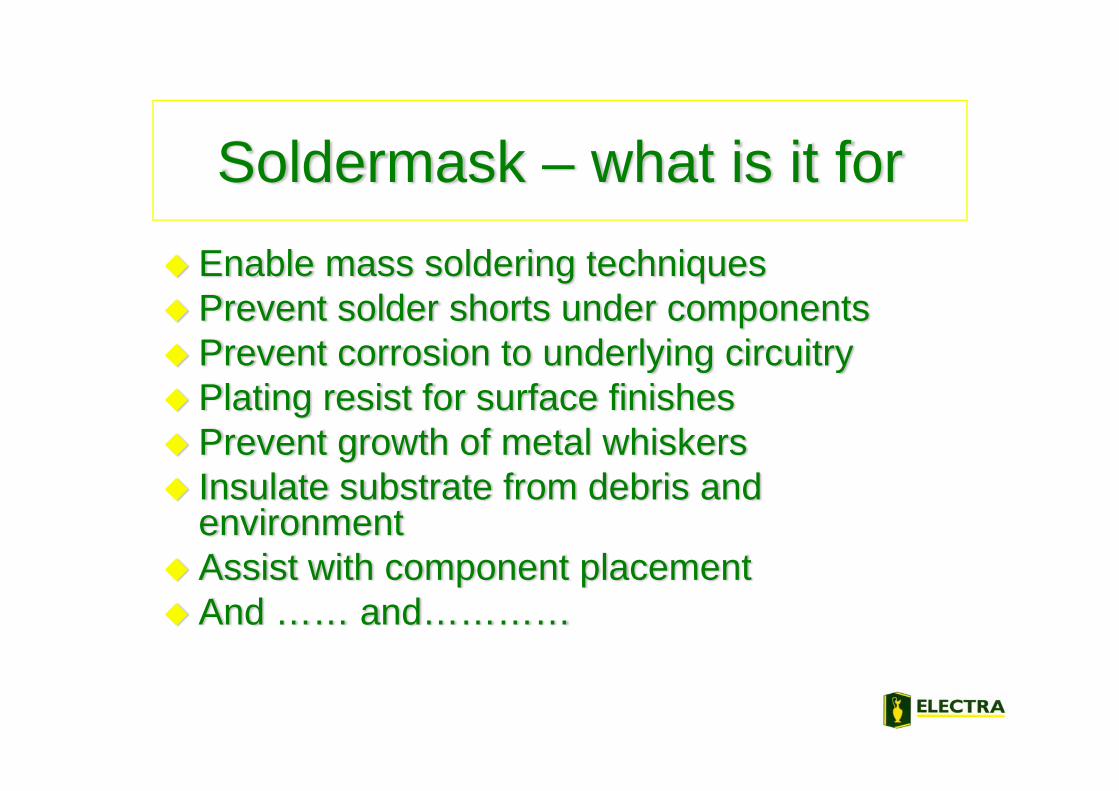
Soldermask – what is it forEnable mass soldering techniquesPrevent solder shorts under componentsPrevent corrosion to underlying circuitryPlating resist for surface finishesPrevent growth of metal whiskersInsulate substrate from debris and environmentAssist with component placementAnd …… and…………

PCB considerations for selection of soldermask
Feature size– Via holes– Solder dams
RegistrationElectrical performance– Impedance control
Cost!!
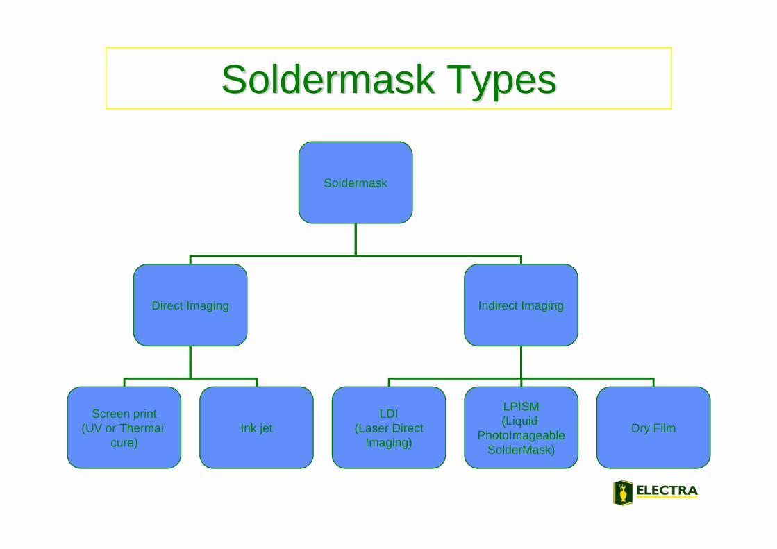
Soldermask Types
Soldermask
Direct Imaging Indirect Imaging
Screen print(UV or Thermal
cure)Ink jet
LDI(Laser Direct
Imaging)
LPISM(Liquid
PhotoImageableSolderMask)
Dry Film

Registration

Registration
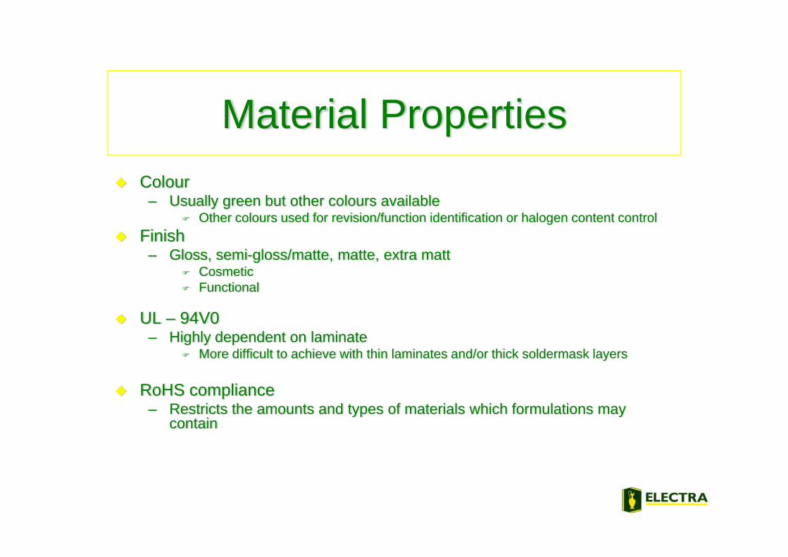
Material PropertiesColour
– Usually green but other colours availableOther colours used for revision/function identification or halogen content control
Finish– Gloss, semi-gloss/matte, matte, extra matt
CosmeticFunctional
UL – 94V0– Highly dependent on laminate
More difficult to achieve with thin laminates and/or thick soldermask layers
RoHS compliance– Restricts the amounts and types of materials which formulations may
contain

Material PropertiesHalogen content– Soldermasks usually contain no bromide (Br -) but may
contain significant amounts of Chloride (Cl-)– Halogen free defined by IEC as:-
<900ppm Cl-<900ppm Br-
<1500ppm X-
Ionic contaminationOutgassing– Important for aerospace and space applications
Solvent emission– VOC & HAP restrictions may influence choice of mask
and/or application method
Compliance
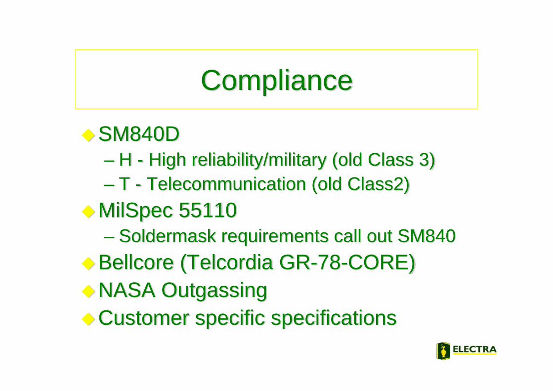
SM840D– H - High reliability/military (old Class 3)– T - Telecommunication (old Class2)
MilSpec 55110– Soldermask requirements call out SM840
Bellcore (Telcordia GR-78-CORE)NASA OutgassingCustomer specific specifications

Process compatibilityPb free processing– 10 - 20deg C higher temperatures put more stress on
soldermask coating ENIG & Imm Sn/Ag resistant– Highly aggressive processes requiring correct selection of
soldermask and good control of application process.Via hole clearing– Smaller vias are harder to clear during development which
may influence choice of mask and application methodVia hole plugging– Tenting not possible with liquid soldermasks– May require separate via-plugging step– Via-in-pad requires planarisation and plating. High solids
better to avoid shrinkage.

Process compatibilitySolder balling– Some assembly processes tend to formation of solderballs
on soldering.– Use of extra-matte soldermasks can help to eliminate
solderballsAssembly materials– Fluxes/cleaners
Zero-solids fluxes provide less thermal barrier to soldermask during wave soldering
– Underfills/adhesivesConformal coating compatibility– Important to evaluate conformal coating/soldermask
combination to ensure good coating/adhesion

Application
Coating methods– Influence on soldermask performance
Coverage profile– Track encapsulation– Resolution of fine features– Influence on PCB electrical performance
Via plugging/cleaning– Environmental concerns
Solvent emissions

Screen print
– Single sideHorizontal orientationGood for thin core/flexible substrate
– Double sidedVertical orientationGood for thin core/flexible substrate
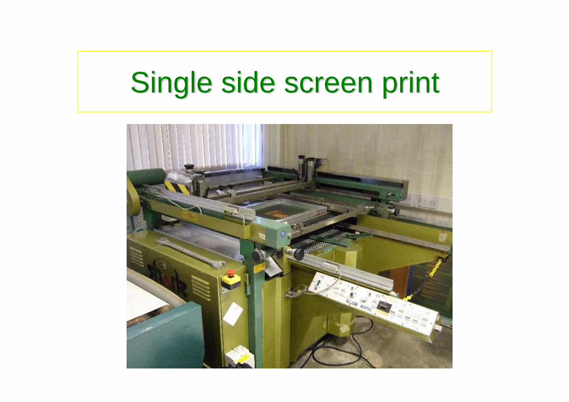
Single side screen print
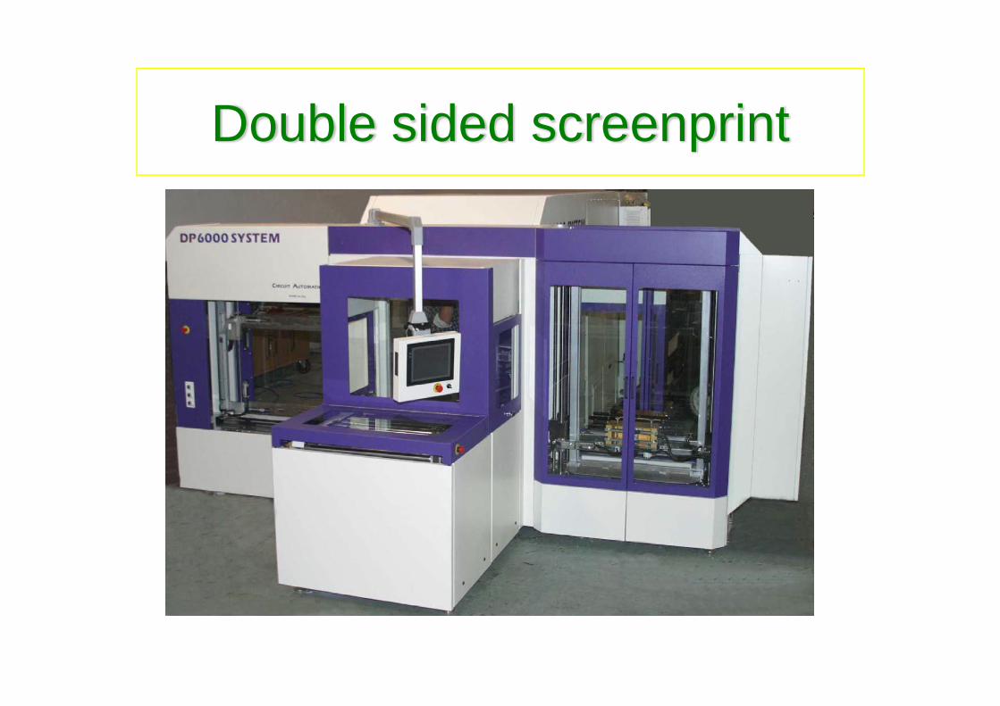
Double sided screenprint
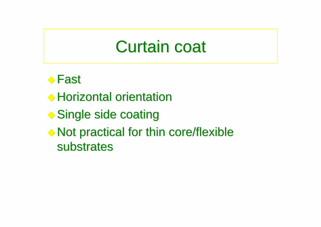
Curtain coat
FastHorizontal orientationSingle side coatingNot practical for thin core/flexible substrates
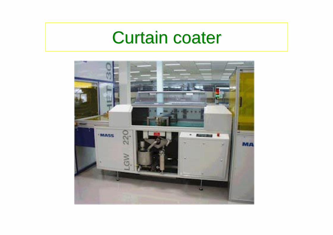
Curtain coater
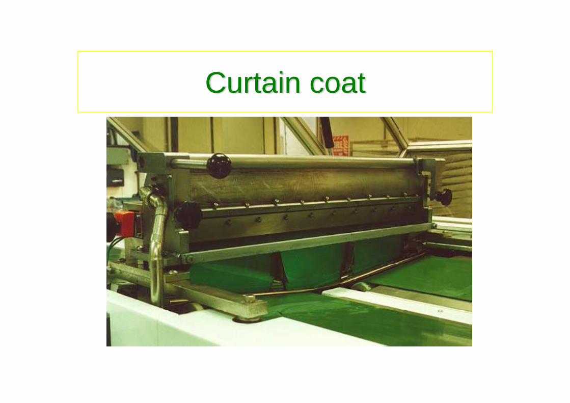
Curtain coat

HPLV Air spray
Horizontal (usually) orientation
Single or double sided coating
Difficult for thin core/flexible substrates
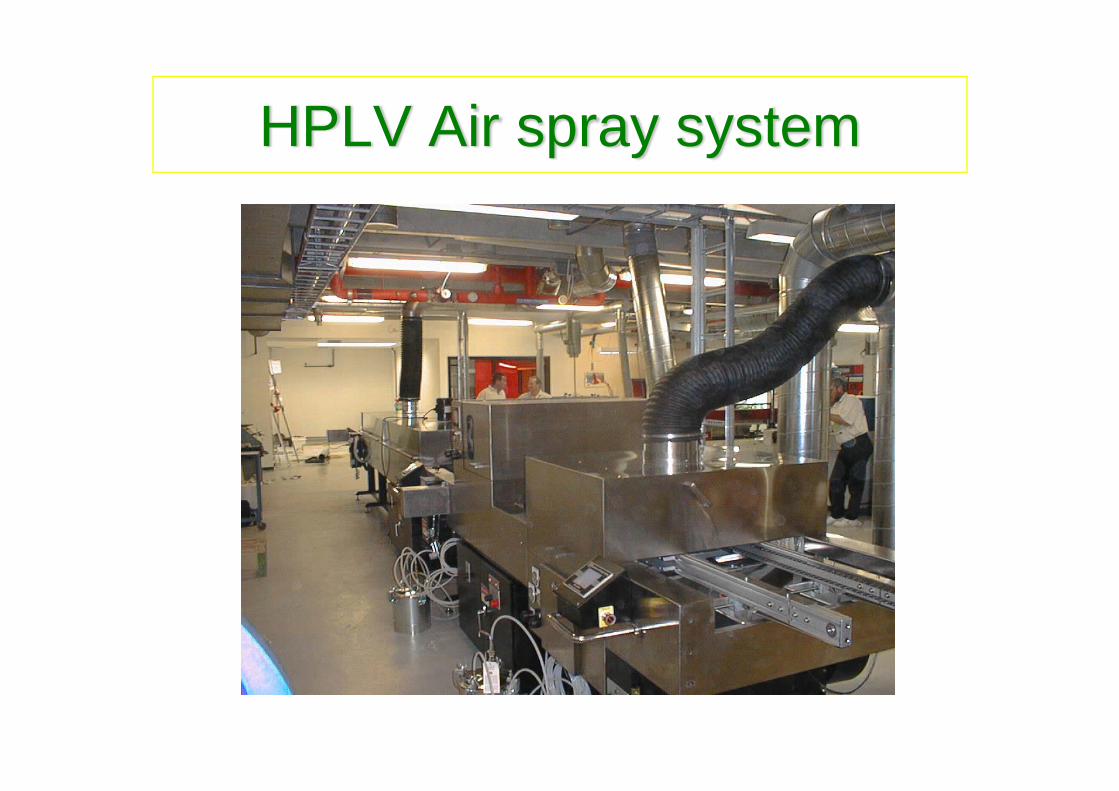
HPLV Air spray system
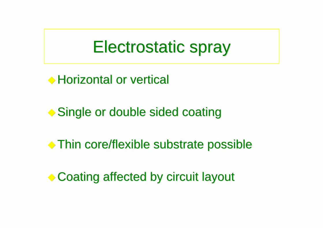
Electrostatic spray
Horizontal or vertical
Single or double sided coating
Thin core/flexible substrate possible
Coating affected by circuit layout
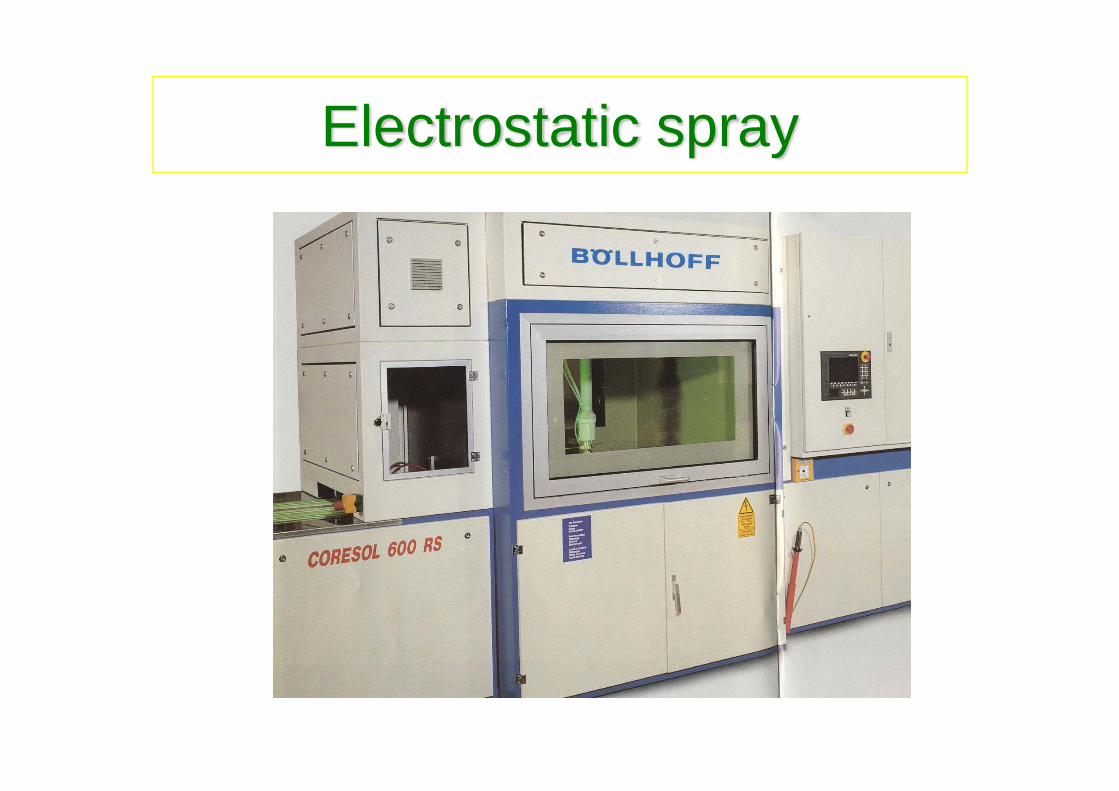
Electrostatic spray

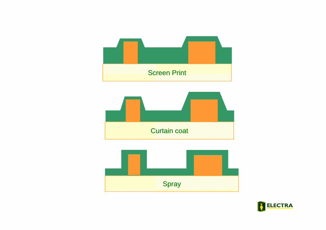
Coating profile
Screen Print – Uniform coating to the board surface– Reasonable track coverage– Moderate amount of mask between tracks
Curtain coat– Uniform coating on board surface– Difficult to coat high/closely spaced tracks – Moderate amount of ink between tracks with little
on top/edges of high/narrow tracks
Coating profile
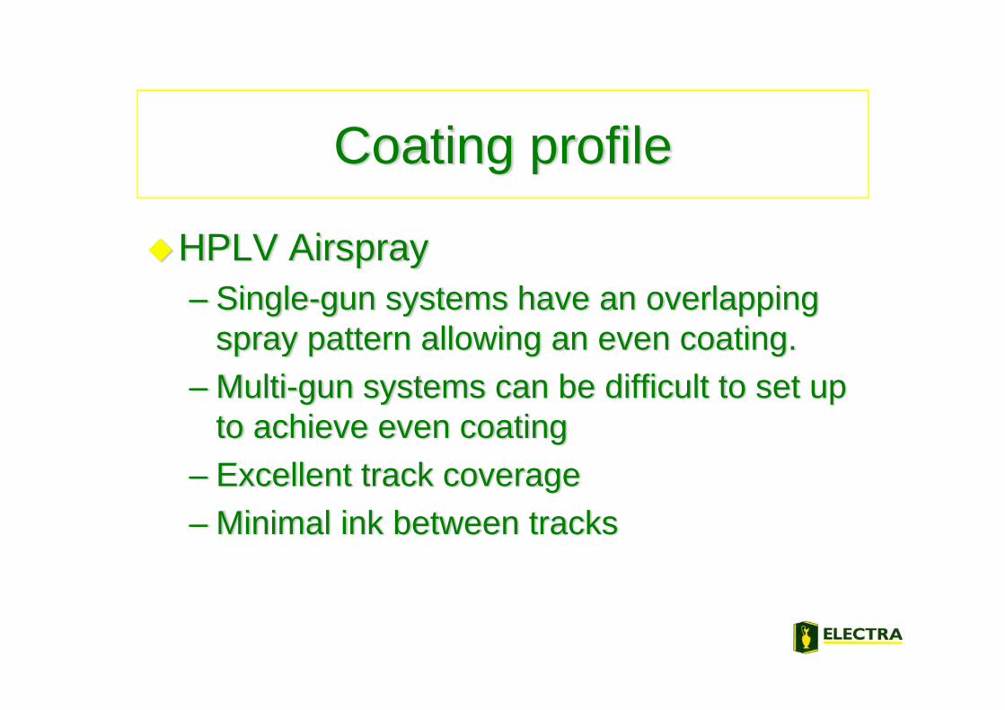
HPLV Airspray– Single-gun systems have an overlapping
spray pattern allowing an even coating.– Multi-gun systems can be difficult to set up
to achieve even coating– Excellent track coverage– Minimal ink between tracks
Coating profile
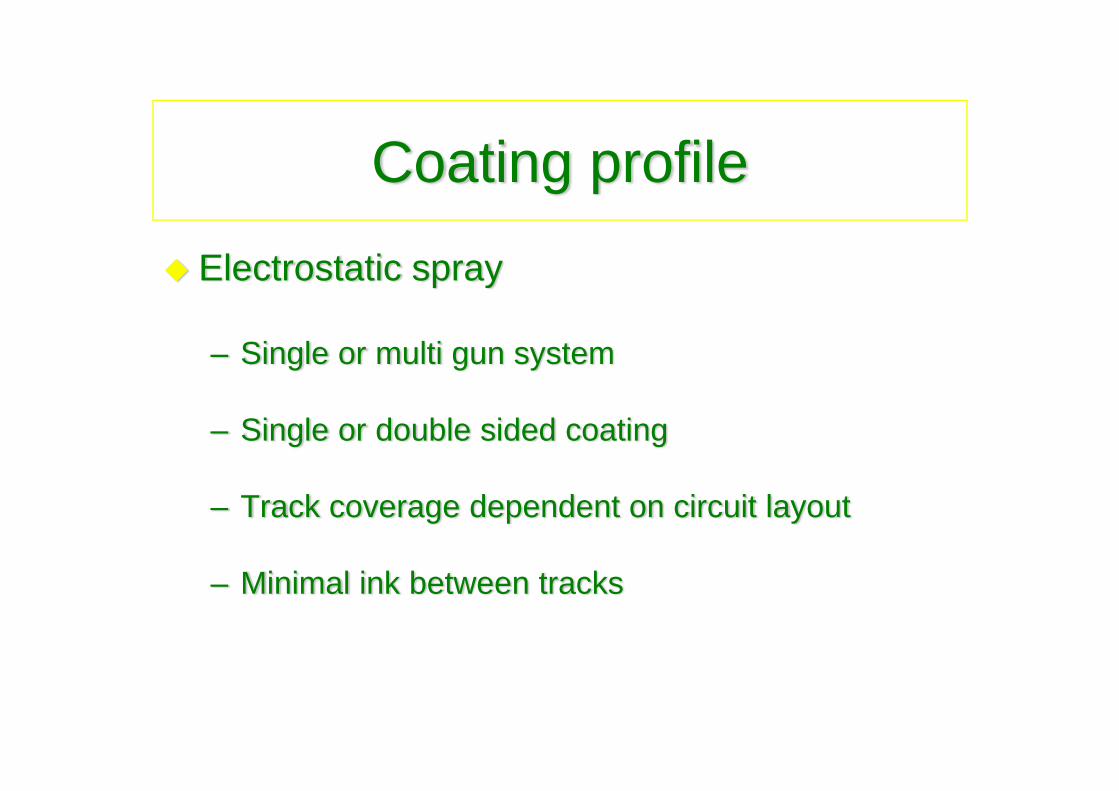
Electrostatic spray
– Single or multi gun system
– Single or double sided coating
– Track coverage dependent on circuit layout
– Minimal ink between tracks
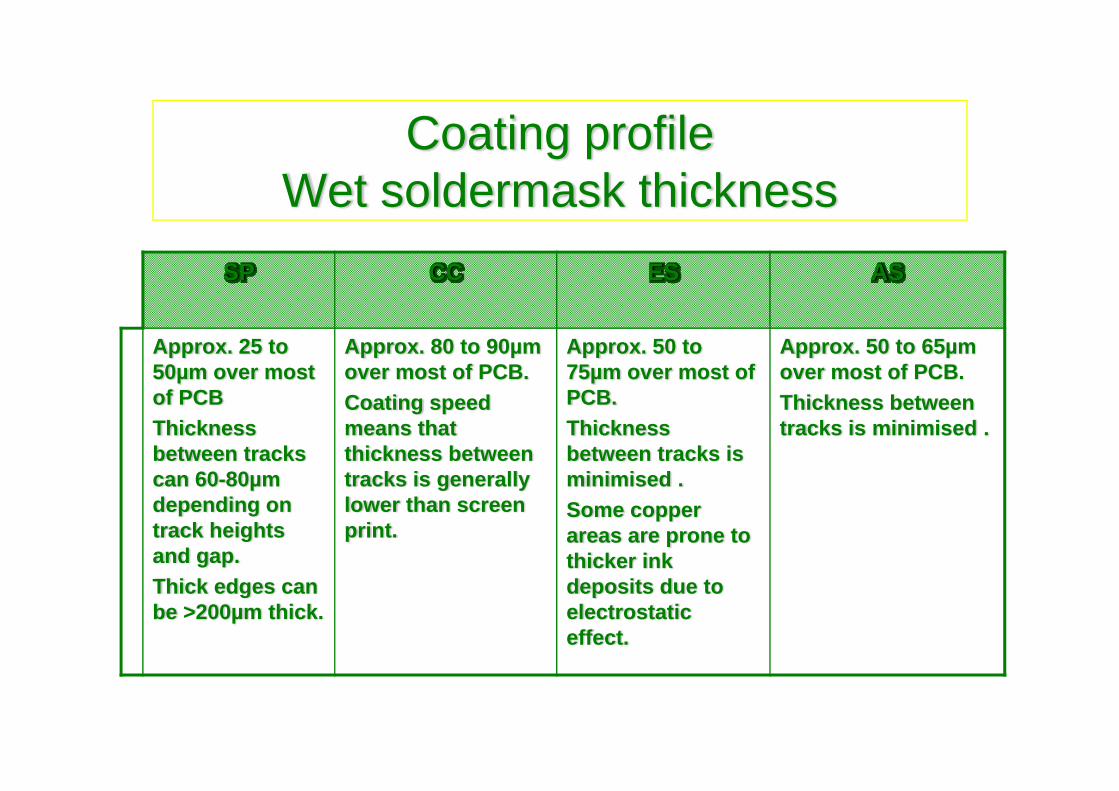
Coating profileWet soldermask thickness
SP CC ES AS
Approx. 25 to 50µm over most of PCBThickness between tracks can 60-80µm depending on track heights and gap.Thick edges can be >200µm thick.
Approx. 80 to 90µm over most of PCB.Coating speed means that thickness between tracks is generally lower than screen print.
Approx. 50 to 75µm over most of PCB.Thickness between tracks is minimised .Some copper areas are prone to thicker ink deposits due to electrostatic effect.
Approx. 50 to 65µm over most of PCB.Thickness between tracks is minimised .
Spray
Screen Print
Curtain coat

Single-Gun Air-spray Coating uniformity
Thickness UniformitySingle gun Air-spray at 1.2 m/min
Area(thou) (microns)
1 1.16 29.5 Mean dry thickness: 30.4 microns2 1.14 29.03 1.22 31.0 Standard deviation: 0.7 microns4 1.19 30.25 1.17 29.7 UCL 32.6 microns6 1.17 29.7 LCL 28.2 microns7 1.23 31.28 1.21 30.79 1.18 30.010 1.18 30.011 1.19 30.212 1.22 31.013 1.21 30.714 1.26 32.015 1.19 30.216 1.19 30.217 1.22 31.018 1.23 31.219 1.17 29.720 1.19 30.2
Dry Thickness

Track encapsulation
• HPLV spray• 400 micron copper• Blind via coverage
400 µm
54 µm

LPI – Coating
CC v SP v ES/AS
1.00E+001.00E+011.00E+021.00E+031.00E+041.00E+05
0 20 40 60 80 100 120
Shear stress
Rhe
olog
yLo
g Sc
ale
Curtain-coat Screen-print Air-spray
Rheological Comparison of LPI Formulations
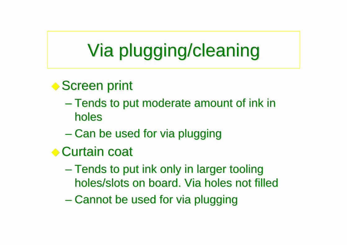
Via plugging/cleaning
Screen print– Tends to put moderate amount of ink in
holes– Can be used for via plugging
Curtain coat– Tends to put ink only in larger tooling
holes/slots on board. Via holes not filled– Cannot be used for via plugging

Via plugging/cleaning
HPLV Airspray– Very little ink in via holes– Cannot be used for via plugging
Electrostatic spray– Very little ink in via holes– Cannot be used for via plugging
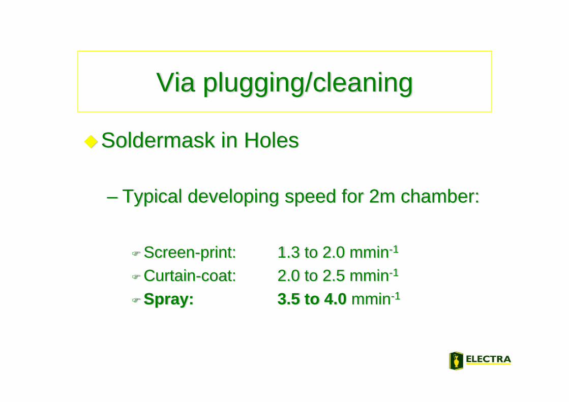
Via plugging/cleaning
Soldermask in Holes
– Typical developing speed for 2m chamber:
Screen-print: 1.3 to 2.0 mmin-1
Curtain-coat: 2.0 to 2.5 mmin-1
Spray: 3.5 to 4.0 mmin-1

Resolution
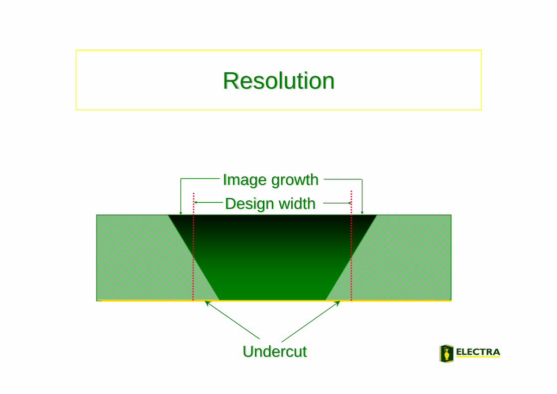
Resolution
Undercut
Design widthImage growth
Resolution
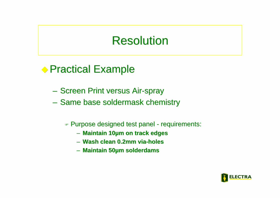
Practical Example
– Screen Print versus Air-spray– Same base soldermask chemistry
Purpose designed test panel - requirements:– Maintain 10µm on track edges– Wash clean 0.2mm via-holes– Maintain 50µm solderdams

High ResolutionScreen Print SM
Dark GreenAir Spray SM
High ResolutionAir Spray SM
Developing Speed
Clean 0.2mm holes
90s dwell
Note: Holes were plugged after printing
30s dwell 30s dwell
Exposure Energy
Hold 50µm dams
583 mJcm-2 270 mJcm-2 134 mJcm-2
Resolution
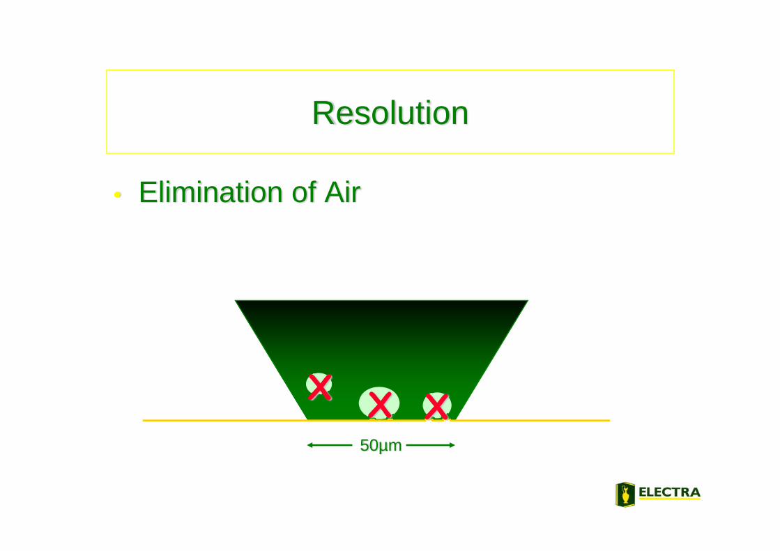
• Elimination of Air
50µm
Resolution
XXX
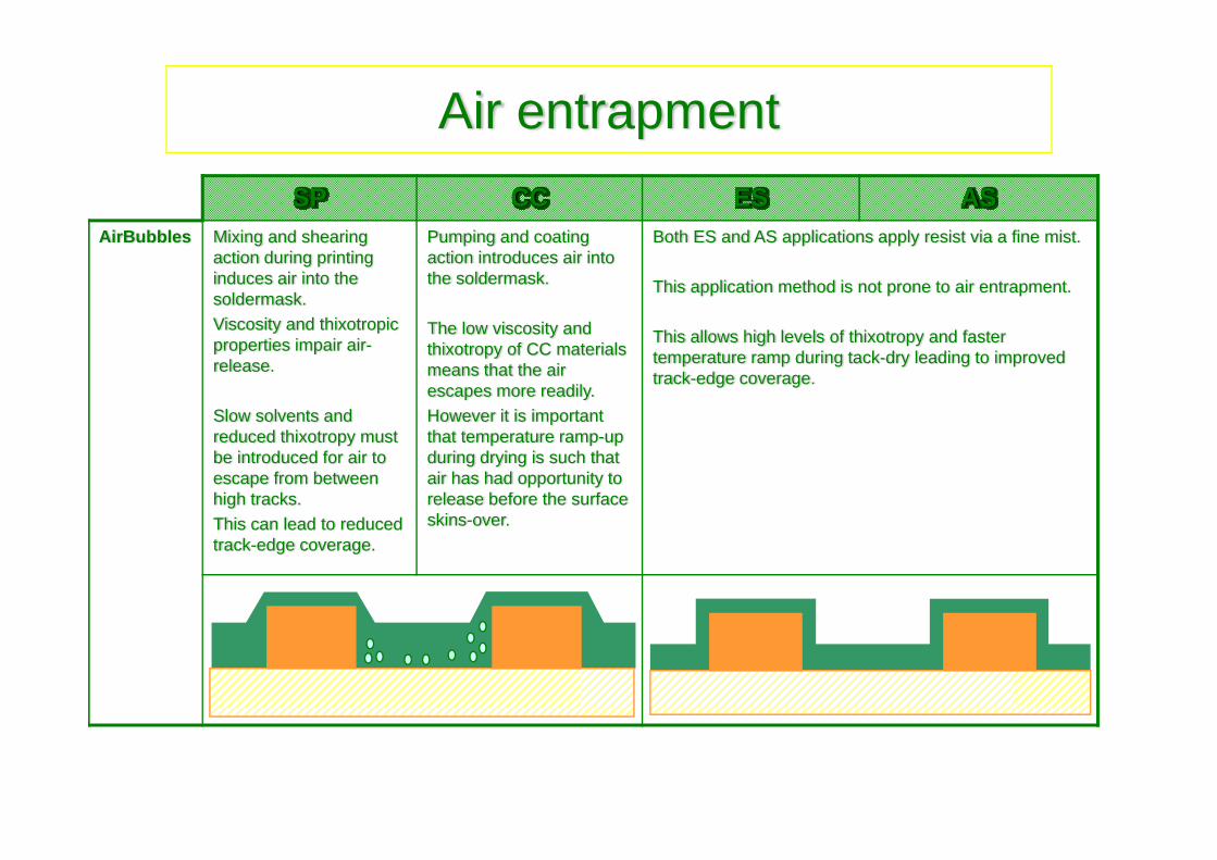
Air entrapmentSP CC ES AS
AirBubbles Mixing and shearing action during printing induces air into the soldermask.Viscosity and thixotropic properties impair air-release.
Slow solvents and reduced thixotropy must be introduced for air to escape from between high tracks. This can lead to reduced track-edge coverage.
Pumping and coating action introduces air into the soldermask.
The low viscosity and thixotropy of CC materials means that the air escapes more readily.However it is important that temperature ramp-up during drying is such that air has had opportunity to release before the surface skins-over.
Both ES and AS applications apply resist via a fine mist.
This application method is not prone to air entrapment.
This allows high levels of thixotropy and faster temperature ramp during tack-dry leading to improved track-edge coverage.
Influence on PCB electrical performance

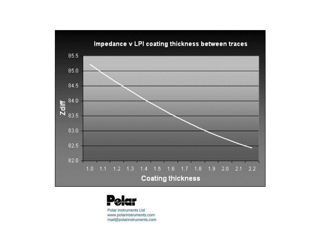
Polar Instruments [email protected]
And finally……
Solvent emissions

Solvent emissions
Application Method Dry Thickness (µm) Coverage (m2kg-1)
SP ≅ 25-30 ≅ 17CC ≅ 40-45 ≅ 12ES ≅ 35-40 ≅ 4.5 to 14AS ≅ 30-35 ≅ 16
Typical Soldermask Consumption (Min. 10µm over 60-70µm tracks)
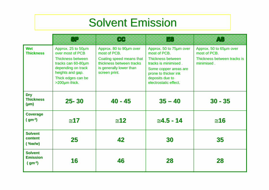
Solvent EmissionSP CC ES AS
Wet Thickness
Approx. 25 to 50µm over most of PCBThickness between tracks can 60-80µm depending on track heights and gap.Thick edges can be >200µm thick.
Approx. 80 to 90µm over most of PCB.Coating speed means that thickness between tracks is generally lower than screen print.
Approx. 50 to 75µm over most of PCB.Thickness between tracks is minimised .Some copper areas are prone to thicker ink deposits due to electrostatic effect.
Approx. 50 to 65µm over most of PCB.Thickness between tracks is minimised .
Dry Thickness (µm) 25- 30 40 - 45 35 – 40 30 - 35
Coverage( gm-2) ≅17 ≅12 ≅4.5 - 14 ≅16
Solvent content( %w/w)
25 42 30 35
Solvent Emission( gm-2) 16 46 28 28

Thank you